US7285844B2 - Multiple internal seal right micro-electro-mechanical system vacuum package - Google Patents
Multiple internal seal right micro-electro-mechanical system vacuum package Download PDFInfo
- Publication number
- US7285844B2 US7285844B2 US10/865,344 US86534404A US7285844B2 US 7285844 B2 US7285844 B2 US 7285844B2 US 86534404 A US86534404 A US 86534404A US 7285844 B2 US7285844 B2 US 7285844B2
- Authority
- US
- United States
- Prior art keywords
- plate
- capping
- base plate
- capping plate
- wafer
- Prior art date
- Legal status (The legal status is an assumption and is not a legal conclusion. Google has not performed a legal analysis and makes no representation as to the accuracy of the status listed.)
- Active, expires
Links
Images


Classifications
-
- G—PHYSICS
- G01—MEASURING; TESTING
- G01C—MEASURING DISTANCES, LEVELS OR BEARINGS; SURVEYING; NAVIGATION; GYROSCOPIC INSTRUMENTS; PHOTOGRAMMETRY OR VIDEOGRAMMETRY
- G01C19/00—Gyroscopes; Turn-sensitive devices using vibrating masses; Turn-sensitive devices without moving masses; Measuring angular rate using gyroscopic effects
- G01C19/56—Turn-sensitive devices using vibrating masses, e.g. vibratory angular rate sensors based on Coriolis forces
- G01C19/5719—Turn-sensitive devices using vibrating masses, e.g. vibratory angular rate sensors based on Coriolis forces using planar vibrating masses driven in a translation vibration along an axis
-
- B—PERFORMING OPERATIONS; TRANSPORTING
- B81—MICROSTRUCTURAL TECHNOLOGY
- B81B—MICROSTRUCTURAL DEVICES OR SYSTEMS, e.g. MICROMECHANICAL DEVICES
- B81B7/00—Microstructural systems; Auxiliary parts of microstructural devices or systems
- B81B7/0032—Packages or encapsulation
- B81B7/007—Interconnections between the MEMS and external electrical signals
Definitions
- the present invention relates to vacuum packages, and particularly to multiple internal seal ring (MISR) micro-electro-mechanical (MEMS) vacuum packages.
- MISR internal seal ring
- MEMS micro-electro-mechanical
- MEMS devices typically integrate both electronic and mechanical elements on a semiconductor wafer using semiconductor fabrication techniques.
- the electronic and mechanical elements are fabricated using a variety of integrated circuit (IC) processing and micromachining techniques, respectively.
- IC integrated circuit
- the cap comprises a capping plate fabricated from a capping wafer that is bonded to a base plate before the base plate wafer is diced or singulated into individual devices.
- the capping plate thus hermetically seals the MEMS devices within the base plate.
- the MEMS devices require electrical connection to external circuits.
- the traces used for connection may create gaps where the capping plate and base plate are bonded.
- the surfaces where the capping plate wafer and the base plate wafer are bonded must be ultra-flat, i.e., polished. This flatness requirement is difficult to meet if additional processing steps are required for bringing electrical feed-through metal traces out through the bonded surfaces. Specifically, bringing electrical wires out through the bonded surfaces requires metal patterning and oxide growth on the wafers' surfaces. Achieving a bond or seal on top of these uneven surfaces is much more difficult.
- the present invention discloses a Multiple Internal Seal Ring (MISR) Micro-Electro-Mechanical System (MEMS) vacuum package that hermetically seals MEMS devices using MISR.
- MISR Multiple Internal Seal Ring
- MEMS Micro-Electro-Mechanical System
- the method bonds a capping plate having metal seal rings to a base plate having metal seal rings by wafer bonding the capping plate wafer to the base plate wafer.
- Bulk electrodes may be used to provide conductive paths between the seal rings on the base plate and the capping plate. All seals are made using only metal-to-metal seal rings deposited on the polished surfaces of the base plate and capping plate wafers.
- each metal seal ring serves the dual purposes of hermetic sealing and providing the electrical feed-through metal trace.
- FIGS. 1A , 1 B and 1 C are perspective views of an embodiment of the present invention, wherein FIG. 1A comprises a base plate, FIG. 1B comprises a capping plate and FIG. 1C shows the final sealed multiple internal seal ring vacuum package;
- FIGS. 2A , 2 B and 2 C are perspective views of the results of wafer scale processing of the vacuum package before singulation, wherein FIG. 2A illustrates bonded wafers containing a plurality of micro-electro-mechanical system devices that are vacuum sealed simultaneously during wafer bonding of a wafer containing the base plates and a wafer containing the capping plates, FIG. 2B is a magnified view of a portion of the bonded wafers, and FIG. 2C is a magnified view of the final sealed multiple internal seal ring vacuum package comprised of the joined base plate and capping plate found in the portion of the bonded wafers.
- FIG. 3 is a flowchart that illustrates the steps of a first general micro-electro-mechanical system processing paradigm for a surface processed micro-electro-mechanical system device etched directly from the base plate wafer that is vacuum packaged using the capping plate wafer;
- FIGS. 4A-4F illustrate the results of the flowchart of FIG. 3 ;
- FIG. 5 is a flowchart that illustrates the steps of a second general micro-electro-mechanical system processing paradigm for a two-wafer bulk silicon etched micro-electro-mechanical system device etched from a bonded base plate wafer and resonator wafer that is vacuum packaged using the capping plate wafer;
- FIGS. 6A-6G illustrate the results of the flowchart of FIG. 5 ;
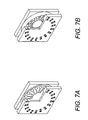
- FIGS. 7A and 7B illustrate a comparison of the multiple internal seal ring vacuum package design for the two-wafer (surface processed micro-electro-mechanical system device) and three-wafer (bulk processed micro-electro-mechanical system device) designs, wherein FIG. 7A is a partially-cutaway view of the two-wafer multiple internal seal ring vacuum package and FIG. 7B is a partially-cutaway view of the three-wafer multiple internal seal ring vacuum package;
- FIG. 8 is a flowchart that illustrates the steps of the three-wafer design packaging a planar gyroscope.
- FIGS. 9A-9I illustrate the results of the flowchart of FIG. 8 .
- the present invention discloses a method of vacuum sealing or hermetically sealing Micro-Electro-Mechanical Systems (MEMS) devices using MISR at a wafer level before singulation or dicing.
- the method bonds a capping plate having metal seal rings to a base plate having metal seal rings by wafer bonding the capping plate wafer to the base plate wafer.
- Bulk electrodes may be used to provide conductive paths between the seal rings on the base plate and the capping plate. This method works best if the bonding surface of the base plate wafer and the bonding surface of the capping plate wafer are ultra-flat (i.e., polished) before the metal seal rings are deposited on each surface.
- All seals are made using only metal-to-metal seal rings deposited on the polished surfaces of the base plate wafer and the capping plate wafer.
- the package still enables multiple electrical feed-through metal traces by fabricating multiple via holes through the capping plate for electrical connection from the outside of the vacuum package through the via-holes to the inside of the vacuum package.
- Each metal seal ring serves the dual purposes of hermetic sealing and providing an electrical feed-through metal trace.
- FIGS. 1A , 1 B and 1 C are perspective views of an embodiment of the present invention, wherein FIG. 1A comprises a base plate 100 , FIG. 1B comprises a capping plate 102 and FIG. 1C shows a final, vacuum-sealed, MISR device package 104 comprised of the bonded base plate 100 and capping plate 102 , wherein the capping plate 102 is flipped before being bonded to the base plate 100 , and the capping plate 102 is shown semi-transparently to better illustrate the components of the package 104 .
- the base plate 100 and the capping plate 102 each include a large periphery seal ring 106 that is used to create one large metal-to-metal seal surrounding the periphery of the package 104 when the base plate 100 and the capping plate 102 are bonded together.
- the base plate 100 and the capping plate 102 each include a plurality of small internal seal rings 108 .
- the seal rings 108 of the base plate 100 each provide an independent electrical path from a cavity 110 of the capping plate 102 where the MEMS device (not shown) resides outward towards the periphery of the package 104 , but not crossing the seal ring 106 .
- Each of the seal rings 108 of the capping plate 102 surround and electrically connect to one of a plurality of via holes 112 on a bottom surface of the capping plate 102 .
- Each via hole 112 extends through the capping plate 102 to a top surface of the capping plate 102 , where the via hole 112 electrically connects to an electrical trace pattern 114 and solder bump 116 on the top surface of the capping plate 102 .
- the package 104 is sealed by compression bonding of the metal-to-metal seal rings 106 and 108 , which is followed by singulation to separate the multiple packages 104 on the bonded wafers.
- FIGS. 1A , 1 B and 1 C illustrate only a single package 104 , the potential benefits (cost savings and simplified, more reliable manufacturing process) of the MISR device package 104 are most dramatic when performed by wafer scale processing.
- FIGS. 2A , 2 B and 2 C are perspective views of the results of wafer scale processing of the package 104 before singulation, wherein FIG. 2A illustrates bonded wafers 200 containing a plurality of MEMS devices that are sealed simultaneously during wafer bonding of a wafer containing the base plates 100 and a wafer containing the capping plates 102 , FIG. 2B is a magnified view of a portion 202 of the bonded wafers 200 , and FIG. 2C is a magnified view of final, vacuum-sealed, MISR device package 104 comprised of the joined base plate 100 and capping plate 102 found in the portion 202 of the bonded wafers 200 .
- FIGS. 4A-4F show a base plate 400 , capping plate 402 , package 404 , large external seal rings 406 , small internal seal rings 408 , etched cavity 410 of the capping plate 402 , etched via holes 412 in the capping plate 402 , electrical trace patterns 414 and solder bumps 416 .
- Blocks 300 and 302 of FIG. 3 illustrate the processing of the base plate 400 , which is generally comprised of silicon or other semiconducting material, and which is illustrated in FIG. 4A .
- Block 300 represents the etching of the base plate 400 in a manner that avoids etching under seal rings 406 and 408 .
- Block 302 represents the metal patterning of the seal rings 406 and 408 .
- Blocks 304 and 306 of FIG. 3 illustrate the processing of the capping plate 402 , which is generally comprised of glass or other non-conducting material, and which is illustrated in FIG. 4B .
- Block 304 represents the etching of the via holes 412 and cavity 410 (if needed) in the capping plate 402 .
- Block 306 represents the metal patterning of the seal rings 406 and 408 on the bottom surface of the capping plate 402 .
- Blocks 308 and 310 of FIG. 3 illustrate the bonding of the base plate 400 and the capping plate 402 , which is illustrated in FIG. 4C .
- Block 308 represents the aligning of the base plate 400 and capping plate 402 wafers, which includes the aligning of the seal rings 406 and 408 of the base plate 400 and capping plate 402 .
- Block 310 represents the bonding of the base plate 400 and capping plate 402 wafers using heat and pressure in an evacuated chamber.
- Blocks 312 and 314 of FIG. 3 illustrate the plating of the capping plate 402 , which is illustrated in FIG. 4D .
- Block 312 represents the electro-less plating of a thin metal layer on the top surface of the capping plate 402 , including inside the via holes 412 .
- Block 314 represents the electroplating of a thicker metal layer on top of the thin metal layer.
- Block 316 of FIG. 3 illustrates the patterning of the electrical trace patterns 414 on the surface of the capping plate 402 , which is illustrated in FIG. 4E .
- Block 316 represents the masking and etching of the electrical trace patterns 414 on the top surface of the capping plate 402 .
- Block 318 of FIG. 3 illustrates the final processing prior to singulation, which is illustrated in FIG. 4E .
- Block 318 represents the depositing of the solder bumps 416 at one end of the electrical trace patterns 414 etched on the top surface of the capping plate 402 , in order to complete the package 404 .
- FIGS. 6A-6G show a base plate 600 , capping plate 602 , package 604 , large external seal rings 606 , small internal seal rings 608 , etched cavity 610 of the capping plate 602 , etched via holes 612 in the capping plate 602 , electrical trace patterns 614 and solder bumps 616 .
- resonator plate 618 that is used to create a MEMS device resonator (not shown), wherein the resonator plate 618 includes bulk electrodes 620 that provide conductive paths between the seal rings 606 and 608 on both the base plate 600 and capping plate 602 .
- Blocks 500 and 502 of FIG. 5 illustrate the processing of the base plate 600 , which is generally comprised of silicon or other semiconducting material, and which is illustrated in FIG. 6A .
- Block 500 represents the etching of the base plate 600 in a manner that avoids etching under seal rings 606 and 608 .
- Block 502 represents the metal patterning of the seal rings 606 and 608 .
- Blocks 504 and 506 of FIG. 5 illustrate the vacuum bonding of the base plate 600 and the resonator plate 616 , which is illustrated in FIG. 6B .
- Block 504 represents the aligning of the base plate 602 and resonator plate 616 wafers.
- Block 506 represents the bonding of the base plate 602 and resonator plate 618 wafers using heat and pressure in an evacuated chamber.
- Block 508 of FIG. 5 illustrates the etching of the resonator plate 616 , which is generally comprised of silicon or other semiconducting material, and which is illustrated in FIG. 6C .
- Block 508 represents the etching of the MEMS resonator (not shown) and bulk electrodes 620 , wherein the doped silicon or a metalization of the resonator plate 618 provides conductive paths for the electrodes 620 .
- Blocks 510 and 512 of FIG. 5 illustrate the processing of the capping plate 602 , which is preferably comprised of glass or other non-conducting material, and which is illustrated in FIG. 6D .
- Block 510 represents the etching of the via holes 612 and cavity 610 (if needed) of the capping plate 602 .
- Block 512 represents the metal patterning of the seal rings 606 and 608 on the bottom surface of the capping plate 602 .
- Blocks 514 and 516 of FIG. 5 illustrate the bonding of the resonator plate 616 and capping plate 602 wafers, which is illustrated in FIG. 6E .
- Block 514 represents the aligning of the resonator plate 618 and capping plate 602 wafers, and more specifically, the aligning of the bulk electrodes 620 of the resonator plate 618 with the seal rings 606 and 608 of the capping plate 602 .
- Block 516 represents the bonding of the resonator plate 618 and capping plate 602 wafers using heat and pressure in an evacuated chamber.
- Blocks 518 and 520 of FIG. 5 illustrate the metal plating of the capping plate 602 , which is illustrated in FIG. 6F .
- Block 518 represents the electro-less plating of a thin metal layer on a top surface of the capping plate 602 including inside the via holes 612 .
- Block 520 represents the electroplating of a thicker metal layer on the thin metal layer.
- Blocks 522 and 524 of FIG. 5 illustrate the final processing, which is illustrated in FIG. 6G .
- Block 522 represents the masking and etching of the electrical trace pattern 614 on the top surface of the capping plate 602 .
- Block 524 represents the depositing of the solder bumps 616 at one end of the electrical trace pattern 614 etched on the top surface of the capping plate 602 , in order to complete the package 604 .
- FIGS. 7A and 7B A comparison of the MISR vacuum package design for the two-wafer (surface processed MEMS device) and three-wafer (two-wafer bulk-silicon-etched MEMS device) are shown in the cutaway views of FIGS. 7A and 7B , wherein FIG. 7A is a partially-cutaway view of the two-wafer MISR package and FIG. 7B is a partially-cutaway view of the three-wafer MISR package.
- FIGS. 6A-6G and 7 B may be used to vacuum package a planar gyroscope described in co-pending U.S. Utility patent application Ser. No. 10/639,134, filed Aug. 12, 2003, by Kirill V. Shcheglov and A. Dorian Challoner, entitled ISOLATED PLANAR GYROSCOPE WITH INTERNAL RADIAL SENSING AND ACTUATION, and which application is incorporated by reference herein. However, certain modifications to the package are required.
- the planar gyroscope has a large total number of electrodes (48 individual electrode elements). If all of these electrodes were brought out of the package through individual seal rings, the increase in total die area would be prohibitive. This is because a “sealing bulk electrode” must have a large enough diameter to support a good vacuum seal. To avoid having 48 sealing bulk electrodes, electrical connections crisscrossing inside the package are used to connect common sets of electrodes. In the planar gyroscope design, the 48 individual electrodes are reduced to only 12 electrode sets requiring individual package feed-throughs. Thus only 12 sealing bulk electrodes are needed in the final design, and these easily fit into the unused comers of the square planar package.
- the internal wire routing (connecting the 48 individual electrodes into 12 sets) requires crossing some wires, and thus requires at least two metal routing layers.
- the design of the MISR package allows this to be achieved without requiring an extra metalization and oxide growth process (which would interfere with the surface flatness required for good sealing).
- This crisscrossing of wires is achieved by using small “bridging bulk electrodes” to act as vias between the base plate's metal patterning and the capping plate's internal metal pattern.
- 48 of these small bridging bulk electrodes are used (to connect each individual electrode with a circular shorting pattern on the capping plate) and 12 sealing bulk electrodes are used to provide the final package feed-throughs for each electrode set.
- Block 800 represents the etching of the base plate 900 , which is illustrated in FIG. 9A .
- Block 802 represents the metal patterning of the base plate 900 , which is illustrated in FIG. 9B .
- Block 804 represents the aligning of the base plate 900 and resonator plate 902 , which was processed separately, and which is illustrated in FIG. 9C .
- Block 806 represents the bonding of the base plate 900 and resonator plate 902 , which is illustrated in FIG. 9D .
- Block 808 represents the deep silicon etching of the resonator plate 902 , which is illustrated in FIG. 9E .
- Block 810 represents the aligning of the base plate 900 and capping plate 904 , which was processed separately, and which is illustrated in FIG. 9F .
- Block 812 represents the bonding of the base plate 900 and capping plate 904 , which is illustrated in FIG. 9G .
- Block 814 represents the electro-less plating of the capping plate 904 , including its via holes 906 , which is illustrated in FIG. 9H .
- Block 816 represents the electroplating of the capping plate 904 , including its via holes 906 , which is also illustrated in FIG. 9H .
- Block 818 represents the masking and etching of the electrical trace pattern 908 on the top surface of the capping plate 904 , which is illustrated in FIG. 9I .
- Block 820 represents the depositing of the solder bumps 910 at one end of the electrical trace pattern 908 etched on the top surface of the capping plate 904 , which is also illustrated in FIG. 9I .
Abstract
Description
Claims (15)
Priority Applications (2)
| Application Number | Priority Date | Filing Date | Title |
|---|---|---|---|
| US10/865,344 US7285844B2 (en) | 2003-06-10 | 2004-06-10 | Multiple internal seal right micro-electro-mechanical system vacuum package |
| US11/850,458 US7396478B2 (en) | 2003-06-10 | 2007-09-05 | Multiple internal seal ring micro-electro-mechanical system vacuum packaging method |
Applications Claiming Priority (2)
| Application Number | Priority Date | Filing Date | Title |
|---|---|---|---|
| US47746303P | 2003-06-10 | 2003-06-10 | |
| US10/865,344 US7285844B2 (en) | 2003-06-10 | 2004-06-10 | Multiple internal seal right micro-electro-mechanical system vacuum package |
Related Child Applications (1)
| Application Number | Title | Priority Date | Filing Date |
|---|---|---|---|
| US11/850,458 Division US7396478B2 (en) | 2003-06-10 | 2007-09-05 | Multiple internal seal ring micro-electro-mechanical system vacuum packaging method |
Publications (2)
| Publication Number | Publication Date |
|---|---|
| US20050017329A1 US20050017329A1 (en) | 2005-01-27 |
| US7285844B2 true US7285844B2 (en) | 2007-10-23 |
Family
ID=34083205
Family Applications (2)
| Application Number | Title | Priority Date | Filing Date |
|---|---|---|---|
| US10/865,344 Active 2025-05-15 US7285844B2 (en) | 2003-06-10 | 2004-06-10 | Multiple internal seal right micro-electro-mechanical system vacuum package |
| US11/850,458 Active US7396478B2 (en) | 2003-06-10 | 2007-09-05 | Multiple internal seal ring micro-electro-mechanical system vacuum packaging method |
Family Applications After (1)
| Application Number | Title | Priority Date | Filing Date |
|---|---|---|---|
| US11/850,458 Active US7396478B2 (en) | 2003-06-10 | 2007-09-05 | Multiple internal seal ring micro-electro-mechanical system vacuum packaging method |
Country Status (1)
| Country | Link |
|---|---|
| US (2) | US7285844B2 (en) |
Cited By (5)
| Publication number | Priority date | Publication date | Assignee | Title |
|---|---|---|---|---|
| US7818871B2 (en) | 2006-07-25 | 2010-10-26 | California Institute Of Technology | Disc resonator gyroscope fabrication process requiring no bonding alignment |
| US10278281B1 (en) | 2015-10-30 | 2019-04-30 | Garmin International, Inc. | MEMS stress isolation and stabilization system |
| US10352960B1 (en) | 2015-10-30 | 2019-07-16 | Garmin International, Inc. | Free mass MEMS accelerometer |
| US10551190B1 (en) | 2015-10-30 | 2020-02-04 | Garmin International, Inc. | Multi Coriolis structured gyroscope |
| US10794700B1 (en) | 2015-10-30 | 2020-10-06 | Garmin International, Inc. | Stress isolation of resonating gyroscopes |
Families Citing this family (12)
| Publication number | Priority date | Publication date | Assignee | Title |
|---|---|---|---|---|
| CA2584851C (en) | 2004-11-04 | 2015-04-07 | Microchips, Inc. | Compression and cold weld sealing methods and devices |
| US7303976B2 (en) * | 2005-05-10 | 2007-12-04 | Hewlett-Packard Development Company, L.P. | Wafer bonding method |
| US7339446B2 (en) * | 2005-06-16 | 2008-03-04 | Intel Corporation | Tunable resonator with MEMS element |
| US7793541B2 (en) * | 2007-06-04 | 2010-09-14 | The Boeing Company | Planar resonator gyroscope central die attachment |
| US7836765B2 (en) * | 2007-07-31 | 2010-11-23 | The Boeing Company | Disc resonator integral inertial measurement unit |
| US8109145B2 (en) * | 2007-07-31 | 2012-02-07 | Northrop Grumman Guidance And Electronics Company, Inc. | Micro hemispheric resonator gyro |
| US7987714B2 (en) * | 2007-10-12 | 2011-08-02 | The Boeing Company | Disc resonator gyroscope with improved frequency coincidence and method of manufacture |
| GB0817309D0 (en) * | 2008-09-19 | 2008-10-29 | Univ Heriot Watt | Encapsulation method |
| US7955885B1 (en) | 2009-01-09 | 2011-06-07 | Integrated Device Technology, Inc. | Methods of forming packaged micro-electromechanical devices |
| US8393212B2 (en) | 2009-04-01 | 2013-03-12 | The Boeing Company | Environmentally robust disc resonator gyroscope |
| US8322028B2 (en) | 2009-04-01 | 2012-12-04 | The Boeing Company | Method of producing an isolator for a microelectromechanical system (MEMS) die |
| US8327526B2 (en) | 2009-05-27 | 2012-12-11 | The Boeing Company | Isolated active temperature regulator for vacuum packaging of a disc resonator gyroscope |
Citations (44)
| Publication number | Priority date | Publication date | Assignee | Title |
|---|---|---|---|---|
| US392650A (en) | 1888-11-13 | watrous | ||
| JPH01129517A (en) | 1987-11-13 | 1989-05-22 | Fujitsu Ltd | Manufacture of surface wave resonance element |
| US4898031A (en) | 1987-07-24 | 1990-02-06 | Yazaki Corporation | Vibrational angular velocity sensor |
| EP0461761A1 (en) | 1990-05-18 | 1991-12-18 | British Aerospace Public Limited Company | Inertial sensors |
| US5203208A (en) | 1991-04-29 | 1993-04-20 | The Charles Stark Draper Laboratory | Symmetrical micromechanical gyroscope |
| US5421312A (en) | 1990-11-03 | 1995-06-06 | Dawson Royalties Limited | Electrical circuit |
| US5507080A (en) * | 1993-12-07 | 1996-04-16 | Matsushita Electric Industrial Co., Ltd. | Method of manufacturing a capacitance sensor |
| DE4442033A1 (en) | 1994-11-25 | 1996-05-30 | Bosch Gmbh Robert | Yaw rate sensor |
| US5578976A (en) | 1995-06-22 | 1996-11-26 | Rockwell International Corporation | Micro electromechanical RF switch |
| WO1996038710A1 (en) | 1995-05-31 | 1996-12-05 | Litef Gmbh | Micromechanical rotation speed sensor |
| US5646346A (en) | 1994-11-10 | 1997-07-08 | Okada; Kazuhiro | Multi-axial angular velocity sensor |
| US5665915A (en) | 1992-03-25 | 1997-09-09 | Fuji Electric Co., Ltd. | Semiconductor capacitive acceleration sensor |
| US5728936A (en) | 1995-08-16 | 1998-03-17 | Robert Bosch Gmbh | Rotary speed sensor |
| WO1998015799A1 (en) | 1996-10-07 | 1998-04-16 | HAHN-SCHICKARD-GESELLSCHAFT FÜR ANGEWANDTE FORSCHUNG E.V. Wilhelm-Schickard-Strasse 10 | Rotation rate sensor with uncoupled mutually perpendicular primary and secondary oscillations |
| US5783749A (en) | 1995-12-07 | 1998-07-21 | Electronics And Telecommunications Research Institute | Vibrating disk type micro-gyroscope |
| DE19719601A1 (en) | 1997-05-09 | 1998-11-12 | Bosch Gmbh Robert | Acceleration sensor with spring-mounted seismic mass |
| US5894090A (en) | 1996-05-31 | 1999-04-13 | California Institute Of Technology | Silicon bulk micromachined, symmetric, degenerate vibratorygyroscope, accelerometer and sensor and method for using the same |
| US5905202A (en) | 1995-09-01 | 1999-05-18 | Hughes Electronics Corporation | Tunneling rotation sensor |
| US5920012A (en) | 1998-06-16 | 1999-07-06 | Boeing North American | Micromechanical inertial sensor |
| US6009751A (en) | 1998-10-27 | 2000-01-04 | Ljung; Bo Hans Gunnar | Coriolis gyro sensor |
| EP0971208A2 (en) | 1998-07-10 | 2000-01-12 | Murata Manufacturing Co., Ltd. | Angular velocity sensor |
| US6044705A (en) | 1993-10-18 | 2000-04-04 | Xros, Inc. | Micromachined members coupled for relative rotation by torsion bars |
| US6145380A (en) | 1997-12-18 | 2000-11-14 | Alliedsignal | Silicon micro-machined accelerometer using integrated electrical and mechanical packaging |
| WO2000068640A2 (en) | 1999-04-21 | 2000-11-16 | The Regents Of The University Of California | Micro-machined angle-measuring gyroscope |
| US6151964A (en) | 1998-05-25 | 2000-11-28 | Citizen Watch Co., Ltd. | Angular velocity sensing device |
| EP1055908A1 (en) | 1999-05-27 | 2000-11-29 | Delphi Technologies, Inc. | Angular rate sensor |
| US6164134A (en) | 1999-01-29 | 2000-12-26 | Hughes Electronics Corporation | Balanced vibratory gyroscope and amplitude control for same |
| US6182352B1 (en) | 1997-06-02 | 2001-02-06 | Avery Dennison Corporation | Method of manufacturing an EAS marker |
| WO2001044823A1 (en) | 1999-12-16 | 2001-06-21 | Robert Bosch Gmbh | Micromechanical spring structure, especially for a rotational speed sensor |
| US6257057B1 (en) * | 1998-12-16 | 2001-07-10 | L-3 Communications Corporation | Epitaxial coriolis rate sensor |
| US6263552B1 (en) | 1995-12-28 | 2001-07-24 | Ngk Insulators, Ltd. | Method of producing piezoelectric/electrostrictive film-type element |
| US6282958B1 (en) | 1998-08-11 | 2001-09-04 | Bae Systems Plc | Angular rate sensor |
| US6289733B1 (en) | 1999-05-12 | 2001-09-18 | Hughes Electronics Corporation | Planar vibratory gyroscopes |
| WO2001074708A2 (en) | 2000-04-05 | 2001-10-11 | Interuniversitair Microelektronica Centrum (Imec) | Method for depositing polycrystalline sige suitable for micromachining and devices obtained thereof |
| US6367786B1 (en) | 1999-06-07 | 2002-04-09 | California Institute Of Technology | Micromachined double resonator |
| US20020066317A1 (en) | 2000-12-06 | 2002-06-06 | Gang Lin | Micro yaw rate sensors |
| US6479320B1 (en) * | 2000-02-02 | 2002-11-12 | Raytheon Company | Vacuum package fabrication of microelectromechanical system devices with integrated circuit components |
| US6481284B2 (en) | 1997-09-02 | 2002-11-19 | Analog Devices, Inc. | Micromachined devices with anti-levitation devices |
| US20030010123A1 (en) | 2000-01-13 | 2003-01-16 | Malvern Alan R | Accelerometer |
| US6515278B2 (en) | 1999-08-05 | 2003-02-04 | Microvision, Inc. | Frequency tunable resonant scanner and method of making |
| US20030029238A1 (en) | 2001-08-10 | 2003-02-13 | The Boeing Company | Isolated resonator gyroscope |
| US6628177B2 (en) | 2000-08-24 | 2003-09-30 | The Regents Of The University Of Michigan | Micromechanical resonator device and micromechanical device utilizing same |
| US20040055380A1 (en) | 2002-08-12 | 2004-03-25 | Shcheglov Kirill V. | Isolated planar gyroscope with internal radial sensing and actuation |
| US6985051B2 (en) | 2002-12-17 | 2006-01-10 | The Regents Of The University Of Michigan | Micromechanical resonator device and method of making a micromechanical device |
Family Cites Families (3)
| Publication number | Priority date | Publication date | Assignee | Title |
|---|---|---|---|---|
| US5297976A (en) * | 1993-05-17 | 1994-03-29 | Electro-Wire Products, Inc. | Sealable electrical connector for an airbag sensor |
| FR2774221B1 (en) * | 1998-01-27 | 2000-04-14 | Legrand France | HOUSING TO BE RECESSED IN ANY WALL, ESPECIALLY FOR AN ELECTRICAL APPARATUS |
| US6944931B2 (en) * | 2002-08-12 | 2005-09-20 | The Boeing Company | Method of producing an integral resonator sensor and case |
-
2004
- 2004-06-10 US US10/865,344 patent/US7285844B2/en active Active
-
2007
- 2007-09-05 US US11/850,458 patent/US7396478B2/en active Active
Patent Citations (49)
| Publication number | Priority date | Publication date | Assignee | Title |
|---|---|---|---|---|
| US392650A (en) | 1888-11-13 | watrous | ||
| US4898031A (en) | 1987-07-24 | 1990-02-06 | Yazaki Corporation | Vibrational angular velocity sensor |
| JPH01129517A (en) | 1987-11-13 | 1989-05-22 | Fujitsu Ltd | Manufacture of surface wave resonance element |
| EP0461761A1 (en) | 1990-05-18 | 1991-12-18 | British Aerospace Public Limited Company | Inertial sensors |
| US5226321A (en) | 1990-05-18 | 1993-07-13 | British Aerospace Public Limited Company | Vibrating planar gyro |
| US5421312A (en) | 1990-11-03 | 1995-06-06 | Dawson Royalties Limited | Electrical circuit |
| US5203208A (en) | 1991-04-29 | 1993-04-20 | The Charles Stark Draper Laboratory | Symmetrical micromechanical gyroscope |
| US5665915A (en) | 1992-03-25 | 1997-09-09 | Fuji Electric Co., Ltd. | Semiconductor capacitive acceleration sensor |
| US5987985A (en) | 1993-03-30 | 1999-11-23 | Okada; Kazuhiro | Angular velocity sensor |
| US6044705A (en) | 1993-10-18 | 2000-04-04 | Xros, Inc. | Micromachined members coupled for relative rotation by torsion bars |
| US5507080A (en) * | 1993-12-07 | 1996-04-16 | Matsushita Electric Industrial Co., Ltd. | Method of manufacturing a capacitance sensor |
| US5646346A (en) | 1994-11-10 | 1997-07-08 | Okada; Kazuhiro | Multi-axial angular velocity sensor |
| DE4442033A1 (en) | 1994-11-25 | 1996-05-30 | Bosch Gmbh Robert | Yaw rate sensor |
| WO1996038710A1 (en) | 1995-05-31 | 1996-12-05 | Litef Gmbh | Micromechanical rotation speed sensor |
| US5578976A (en) | 1995-06-22 | 1996-11-26 | Rockwell International Corporation | Micro electromechanical RF switch |
| US5728936A (en) | 1995-08-16 | 1998-03-17 | Robert Bosch Gmbh | Rotary speed sensor |
| US5905202A (en) | 1995-09-01 | 1999-05-18 | Hughes Electronics Corporation | Tunneling rotation sensor |
| US5783749A (en) | 1995-12-07 | 1998-07-21 | Electronics And Telecommunications Research Institute | Vibrating disk type micro-gyroscope |
| US6263552B1 (en) | 1995-12-28 | 2001-07-24 | Ngk Insulators, Ltd. | Method of producing piezoelectric/electrostrictive film-type element |
| US5894090A (en) | 1996-05-31 | 1999-04-13 | California Institute Of Technology | Silicon bulk micromachined, symmetric, degenerate vibratorygyroscope, accelerometer and sensor and method for using the same |
| WO1998015799A1 (en) | 1996-10-07 | 1998-04-16 | HAHN-SCHICKARD-GESELLSCHAFT FÜR ANGEWANDTE FORSCHUNG E.V. Wilhelm-Schickard-Strasse 10 | Rotation rate sensor with uncoupled mutually perpendicular primary and secondary oscillations |
| DE19719601A1 (en) | 1997-05-09 | 1998-11-12 | Bosch Gmbh Robert | Acceleration sensor with spring-mounted seismic mass |
| US6182352B1 (en) | 1997-06-02 | 2001-02-06 | Avery Dennison Corporation | Method of manufacturing an EAS marker |
| US6481284B2 (en) | 1997-09-02 | 2002-11-19 | Analog Devices, Inc. | Micromachined devices with anti-levitation devices |
| US6145380A (en) | 1997-12-18 | 2000-11-14 | Alliedsignal | Silicon micro-machined accelerometer using integrated electrical and mechanical packaging |
| US6151964A (en) | 1998-05-25 | 2000-11-28 | Citizen Watch Co., Ltd. | Angular velocity sensing device |
| US5920012A (en) | 1998-06-16 | 1999-07-06 | Boeing North American | Micromechanical inertial sensor |
| EP0971208A2 (en) | 1998-07-10 | 2000-01-12 | Murata Manufacturing Co., Ltd. | Angular velocity sensor |
| US6282958B1 (en) | 1998-08-11 | 2001-09-04 | Bae Systems Plc | Angular rate sensor |
| US6009751A (en) | 1998-10-27 | 2000-01-04 | Ljung; Bo Hans Gunnar | Coriolis gyro sensor |
| US6257057B1 (en) * | 1998-12-16 | 2001-07-10 | L-3 Communications Corporation | Epitaxial coriolis rate sensor |
| US6164134A (en) | 1999-01-29 | 2000-12-26 | Hughes Electronics Corporation | Balanced vibratory gyroscope and amplitude control for same |
| WO2000068640A2 (en) | 1999-04-21 | 2000-11-16 | The Regents Of The University Of California | Micro-machined angle-measuring gyroscope |
| US6481285B1 (en) | 1999-04-21 | 2002-11-19 | Andrei M. Shkel | Micro-machined angle-measuring gyroscope |
| US6289733B1 (en) | 1999-05-12 | 2001-09-18 | Hughes Electronics Corporation | Planar vibratory gyroscopes |
| EP1055908A1 (en) | 1999-05-27 | 2000-11-29 | Delphi Technologies, Inc. | Angular rate sensor |
| US6367786B1 (en) | 1999-06-07 | 2002-04-09 | California Institute Of Technology | Micromachined double resonator |
| US6515278B2 (en) | 1999-08-05 | 2003-02-04 | Microvision, Inc. | Frequency tunable resonant scanner and method of making |
| WO2001044823A1 (en) | 1999-12-16 | 2001-06-21 | Robert Bosch Gmbh | Micromechanical spring structure, especially for a rotational speed sensor |
| US20030010123A1 (en) | 2000-01-13 | 2003-01-16 | Malvern Alan R | Accelerometer |
| US6479320B1 (en) * | 2000-02-02 | 2002-11-12 | Raytheon Company | Vacuum package fabrication of microelectromechanical system devices with integrated circuit components |
| WO2001074708A2 (en) | 2000-04-05 | 2001-10-11 | Interuniversitair Microelektronica Centrum (Imec) | Method for depositing polycrystalline sige suitable for micromachining and devices obtained thereof |
| US6628177B2 (en) | 2000-08-24 | 2003-09-30 | The Regents Of The University Of Michigan | Micromechanical resonator device and micromechanical device utilizing same |
| US6856217B1 (en) | 2000-08-24 | 2005-02-15 | The Regents Of The University Of Michigan | Micromechanical resonator device and micromechanical device utilizing same |
| US20020066317A1 (en) | 2000-12-06 | 2002-06-06 | Gang Lin | Micro yaw rate sensors |
| US6629460B2 (en) | 2001-08-10 | 2003-10-07 | The Boeing Company | Isolated resonator gyroscope |
| US20030029238A1 (en) | 2001-08-10 | 2003-02-13 | The Boeing Company | Isolated resonator gyroscope |
| US20040055380A1 (en) | 2002-08-12 | 2004-03-25 | Shcheglov Kirill V. | Isolated planar gyroscope with internal radial sensing and actuation |
| US6985051B2 (en) | 2002-12-17 | 2006-01-10 | The Regents Of The University Of Michigan | Micromechanical resonator device and method of making a micromechanical device |
Non-Patent Citations (14)
| Title |
|---|
| Barbour et al., "Micromechanical Silicon Instrument and Systems Development at Draper Laboratory," AIAA Guidance Navigation and Control Conference, 1996, Paper No. 96-3709. |
| Barbour, N. et al., "Micromechanical Silicon Instrument and Systems Development at Draper Laboratory," 1996, ALAA Guidance, Navigation and Control Conference, 1-7. |
| D. Wright et al., "The HRG Applied to a Satellite Attitude Reference System," Guidance and Control, American Astronautical Society, Advances in Astronautical Sciences, 1994, 86:1-13. |
| Fujita et al., "Disk-shaped bulk micromachined gyroscope with vacuum sealing," Sensors and Actuators A:Physical, vol. 82, May 2000, pp. 198-204. |
| Fujita, T. et al., "Disk-shaped bulk micromachined gyroscope with vacuum sealing," 2000, Sensors and Actuators, 82:198-204. |
| Johnson et al., "Surface Micromachined Angular Rate Sensor," A1995 SAE Conference, Paper No. 950538, pp. 77-83. |
| Johnson, J.D. et al., "Surface Micromachined Angular Rate Sensor," A1995 SAE Conference, Paper No. 950538, pp. 77-83. |
| Putty et al., "A Micromachined Vibrating Ring Gyroscope," Solid State Sensor and Actuator Workshop, Transducer Research Foundation, Hilton Head, 1994, pp. 213-220. |
| Putty, M.W. et al., "A Micromachined Vibrating Ring Gyroscope," 1994, Center for Integrated Sensors and Circuits, 213-220. |
| Skulski et al., "Planar resonator sensor for moisture measurements", Microwaves and Radar, 1998, MIKON '98, 12th International Conf., vol. 3, May 20-22, 1998, pp. 692-695. |
| Skulski, J. et al., "Planar Resonator Sensor for Moisture Measurements," May 20-22, 1998, Microwaves and Radar, 12<SUP>th </SUP>International Conference on MIKON, 3:692-695. |
| T.K. Tang et al., "Silicon Bulk Micromachined Vibratory Gyroscope," Solid State Sensor and Actuator Workshop, Transducer Research Foundation, Hilton Head, South Carolina, Jun. 2-6, 1996, 6 pgs. |
| Tang et al., "A Packaged Silicon MEMS Vibratory Gyroscope for Microspacecraft," Proceedings IEEE, 10<SUP>th </SUP>Annual Int. Workshop on MEMS, Japan, 1997, pp. 500-505. |
| Wright t al., "The HRG Applied to a Satellite Attitude Reference System," Guidance and Control, AASAAS, 1994, 86:1-13. |
Cited By (6)
| Publication number | Priority date | Publication date | Assignee | Title |
|---|---|---|---|---|
| US7818871B2 (en) | 2006-07-25 | 2010-10-26 | California Institute Of Technology | Disc resonator gyroscope fabrication process requiring no bonding alignment |
| US10278281B1 (en) | 2015-10-30 | 2019-04-30 | Garmin International, Inc. | MEMS stress isolation and stabilization system |
| US10352960B1 (en) | 2015-10-30 | 2019-07-16 | Garmin International, Inc. | Free mass MEMS accelerometer |
| US10551190B1 (en) | 2015-10-30 | 2020-02-04 | Garmin International, Inc. | Multi Coriolis structured gyroscope |
| US10794700B1 (en) | 2015-10-30 | 2020-10-06 | Garmin International, Inc. | Stress isolation of resonating gyroscopes |
| US10907965B2 (en) | 2015-10-30 | 2021-02-02 | Garmin International, Inc. | Multi coriolis structured gyroscope |
Also Published As
| Publication number | Publication date |
|---|---|
| US20050017329A1 (en) | 2005-01-27 |
| US7396478B2 (en) | 2008-07-08 |
| US20070298542A1 (en) | 2007-12-27 |
Similar Documents
| Publication | Publication Date | Title |
|---|---|---|
| US7396478B2 (en) | Multiple internal seal ring micro-electro-mechanical system vacuum packaging method | |
| US7026223B2 (en) | Hermetic electric component package | |
| US8143082B2 (en) | Wafer bonding of micro-electro mechanical systems to active circuitry | |
| US6429511B2 (en) | Microcap wafer-level package | |
| JP4486229B2 (en) | Wafer package manufacturing method | |
| KR100907514B1 (en) | Sensor device, sensor system and method of manufacturing the same | |
| EP2121511B1 (en) | Method of packaging an electronic or micromechanical component | |
| US6313529B1 (en) | Bump bonding and sealing a semiconductor device with solder | |
| US9346666B2 (en) | Composite wafer semiconductor | |
| US7868448B2 (en) | Electrical component and production thereof | |
| US20040259325A1 (en) | Wafer level chip scale hermetic package | |
| US7955885B1 (en) | Methods of forming packaged micro-electromechanical devices | |
| US20180362330A9 (en) | Mems components and method of wafer-level manufacturing thereof | |
| US20060211177A1 (en) | Structure and process for packaging RF MEMS and other devices | |
| US20090085191A1 (en) | Environment-Resistant Module, Micropackage And Methods Of Manufacturing Same | |
| US10988373B2 (en) | MEMS component having low-resistance wiring and method for manufacturing it | |
| JP2005129888A (en) | Sensor device and sensor system, and manufacturing method therefor | |
| JP2005019966A (en) | Semiconductor device and method of manufacturing the same | |
| JP2009014469A (en) | Semiconductor device and method for manufacturing the same | |
| EP1199744B1 (en) | Microcap wafer-level package | |
| JP2006186357A (en) | Sensor device and its manufacturing method | |
| JP2006201158A (en) | Sensor | |
| CN105347288A (en) | Multi-device enclosing structure for wafer-level packaging and manufacturing method thereof | |
| CN107697882B (en) | Process for manufacturing a semiconductor device and corresponding semiconductor device | |
| JP2006126212A (en) | Sensor device |
Legal Events
| Date | Code | Title | Description |
|---|---|---|---|
| AS | Assignment |
Owner name: CALIFORNIA INSTITUTE OF TECHNOLOGY, CALIFORNIA Free format text: ASSIGNMENT OF ASSIGNORS INTEREST;ASSIGNORS:HAYWORTH, KEN J.;YEE, KARL Y.;SHCHEGLOV, KIRILL;AND OTHERS;REEL/FRAME:015481/0427 Effective date: 20040610 |
|
| AS | Assignment |
Owner name: THE BOEING COMPANY, ILLINOIS Free format text: ASSIGNMENT OF ASSIGNORS INTEREST;ASSIGNOR:CHALLONER, A. DORIAN;REEL/FRAME:015037/0509 Effective date: 20040819 |
|
| AS | Assignment |
Owner name: NASA, DISTRICT OF COLUMBIA Free format text: CONFIRMATORY LICENSE;ASSIGNOR:CALIFORNIA INSTITUTE OF TECHNOLOGY;REEL/FRAME:015890/0206 Effective date: 20040913 |
|
| AS | Assignment |
Owner name: CALIFORNIA INSTITUTE OF TECHNOLOGY, CALIFORNIA Free format text: ASSIGNMENT OF ASSIGNORS INTEREST;ASSIGNOR:BAC, YOUNGSAM;REEL/FRAME:015606/0906 Effective date: 20050116 |
|
| AS | Assignment |
Owner name: CALIFORNIA INSTITUTE OF TECHNOLOGY, CALIFORNIA Free format text: CORRECTIVE COVERSHEET TO CORRECT THE NAME OF THE ASSIGNOR PREVIOUSLY RECORDED ON REEL 015606, FRAME 0906.;ASSIGNOR:BAE, YOUNGSAM;REEL/FRAME:015627/0997 Effective date: 20050116 |
|
| STCF | Information on status: patent grant |
Free format text: PATENTED CASE |
|
| FPAY | Fee payment |
Year of fee payment: 4 |
|
| REMI | Maintenance fee reminder mailed | ||
| FPAY | Fee payment |
Year of fee payment: 8 |
|
| SULP | Surcharge for late payment |
Year of fee payment: 7 |
|
| MAFP | Maintenance fee payment |
Free format text: PAYMENT OF MAINTENANCE FEE, 12TH YEAR, LARGE ENTITY (ORIGINAL EVENT CODE: M1553); ENTITY STATUS OF PATENT OWNER: LARGE ENTITY Year of fee payment: 12 |