US7223672B2 - Processes for forming backplanes for electro-optic displays - Google Patents
Processes for forming backplanes for electro-optic displays Download PDFInfo
- Publication number
- US7223672B2 US7223672B2 US10/249,624 US24962403A US7223672B2 US 7223672 B2 US7223672 B2 US 7223672B2 US 24962403 A US24962403 A US 24962403A US 7223672 B2 US7223672 B2 US 7223672B2
- Authority
- US
- United States
- Prior art keywords
- flexible substrate
- substantially rigid
- rigid carrier
- layer
- substrate
- Prior art date
- Legal status (The legal status is an assumption and is not a legal conclusion. Google has not performed a legal analysis and makes no representation as to the accuracy of the status listed.)
- Expired - Lifetime, expires
Links
- 238000000034 method Methods 0.000 title claims abstract description 145
- 230000008569 process Effects 0.000 title claims abstract description 121
- 239000000758 substrate Substances 0.000 claims abstract description 211
- 239000000463 material Substances 0.000 claims abstract description 35
- 230000015572 biosynthetic process Effects 0.000 claims description 19
- 238000000926 separation method Methods 0.000 claims description 17
- 230000005855 radiation Effects 0.000 claims description 16
- 239000004642 Polyimide Substances 0.000 claims description 14
- 239000011521 glass Substances 0.000 claims description 14
- 229920001721 polyimide Polymers 0.000 claims description 14
- 238000002679 ablation Methods 0.000 claims description 8
- 230000005670 electromagnetic radiation Effects 0.000 claims description 8
- 230000004888 barrier function Effects 0.000 claims description 6
- 230000008021 deposition Effects 0.000 claims description 6
- 239000002923 metal particle Substances 0.000 claims description 4
- 238000005530 etching Methods 0.000 abstract description 16
- 239000004065 semiconductor Substances 0.000 abstract description 14
- 238000000151 deposition Methods 0.000 abstract description 10
- 238000000059 patterning Methods 0.000 abstract description 6
- 239000010410 layer Substances 0.000 description 105
- 238000004519 manufacturing process Methods 0.000 description 20
- 229910052751 metal Inorganic materials 0.000 description 20
- 239000002184 metal Substances 0.000 description 20
- 239000010408 film Substances 0.000 description 18
- 229910000831 Steel Inorganic materials 0.000 description 11
- 239000004020 conductor Substances 0.000 description 11
- 230000003287 optical effect Effects 0.000 description 11
- 239000010959 steel Substances 0.000 description 11
- 238000007639 printing Methods 0.000 description 10
- 239000013047 polymeric layer Substances 0.000 description 9
- 238000000576 coating method Methods 0.000 description 8
- 239000004973 liquid crystal related substance Substances 0.000 description 8
- 238000012546 transfer Methods 0.000 description 8
- 229910021417 amorphous silicon Inorganic materials 0.000 description 7
- 239000011248 coating agent Substances 0.000 description 7
- 239000011159 matrix material Substances 0.000 description 7
- 239000002245 particle Substances 0.000 description 7
- 238000000206 photolithography Methods 0.000 description 7
- 229920002120 photoresistant polymer Polymers 0.000 description 7
- 229920000642 polymer Polymers 0.000 description 7
- 239000010409 thin film Substances 0.000 description 7
- 238000013459 approach Methods 0.000 description 5
- 239000002775 capsule Substances 0.000 description 5
- 239000010935 stainless steel Substances 0.000 description 5
- 229910001220 stainless steel Inorganic materials 0.000 description 5
- 239000000126 substance Substances 0.000 description 5
- 229910052581 Si3N4 Inorganic materials 0.000 description 4
- 238000010521 absorption reaction Methods 0.000 description 4
- 238000003491 array Methods 0.000 description 4
- 239000003990 capacitor Substances 0.000 description 4
- 230000008859 change Effects 0.000 description 4
- 230000005684 electric field Effects 0.000 description 4
- 239000012530 fluid Substances 0.000 description 4
- 230000006872 improvement Effects 0.000 description 4
- 239000007788 liquid Substances 0.000 description 4
- HQVNEWCFYHHQES-UHFFFAOYSA-N silicon nitride Chemical compound N12[Si]34N5[Si]62N3[Si]51N64 HQVNEWCFYHHQES-UHFFFAOYSA-N 0.000 description 4
- 239000012790 adhesive layer Substances 0.000 description 3
- 230000008901 benefit Effects 0.000 description 3
- 239000003989 dielectric material Substances 0.000 description 3
- 239000000976 ink Substances 0.000 description 3
- 239000003094 microcapsule Substances 0.000 description 3
- 230000004048 modification Effects 0.000 description 3
- 238000012986 modification Methods 0.000 description 3
- 239000000382 optic material Substances 0.000 description 3
- 238000001020 plasma etching Methods 0.000 description 3
- 238000012545 processing Methods 0.000 description 3
- 230000002829 reductive effect Effects 0.000 description 3
- 238000009420 retrofitting Methods 0.000 description 3
- 238000005382 thermal cycling Methods 0.000 description 3
- 238000003466 welding Methods 0.000 description 3
- CFAKWWQIUFSQFU-UHFFFAOYSA-N 2-hydroxy-3-methylcyclopent-2-en-1-one Chemical compound CC1=C(O)C(=O)CC1 CFAKWWQIUFSQFU-UHFFFAOYSA-N 0.000 description 2
- 239000004593 Epoxy Substances 0.000 description 2
- 239000000853 adhesive Substances 0.000 description 2
- 230000001070 adhesive effect Effects 0.000 description 2
- 229910052782 aluminium Inorganic materials 0.000 description 2
- XAGFODPZIPBFFR-UHFFFAOYSA-N aluminium Chemical compound [Al] XAGFODPZIPBFFR-UHFFFAOYSA-N 0.000 description 2
- 238000002048 anodisation reaction Methods 0.000 description 2
- 230000005540 biological transmission Effects 0.000 description 2
- 239000002131 composite material Substances 0.000 description 2
- 238000011109 contamination Methods 0.000 description 2
- 230000032798 delamination Effects 0.000 description 2
- 238000003618 dip coating Methods 0.000 description 2
- 230000000694 effects Effects 0.000 description 2
- 239000011888 foil Substances 0.000 description 2
- 230000006870 function Effects 0.000 description 2
- 238000003384 imaging method Methods 0.000 description 2
- 229910052738 indium Inorganic materials 0.000 description 2
- APFVFJFRJDLVQX-UHFFFAOYSA-N indium atom Chemical compound [In] APFVFJFRJDLVQX-UHFFFAOYSA-N 0.000 description 2
- 239000012212 insulator Substances 0.000 description 2
- 238000003475 lamination Methods 0.000 description 2
- 238000004377 microelectronic Methods 0.000 description 2
- 230000002093 peripheral effect Effects 0.000 description 2
- 238000000053 physical method Methods 0.000 description 2
- 238000007650 screen-printing Methods 0.000 description 2
- 210000003934 vacuole Anatomy 0.000 description 2
- 239000001837 2-hydroxy-3-methylcyclopent-2-en-1-one Substances 0.000 description 1
- OKTJSMMVPCPJKN-UHFFFAOYSA-N Carbon Chemical compound [C] OKTJSMMVPCPJKN-UHFFFAOYSA-N 0.000 description 1
- 229920001730 Moisture cure polyurethane Polymers 0.000 description 1
- 239000004983 Polymer Dispersed Liquid Crystal Substances 0.000 description 1
- 238000007754 air knife coating Methods 0.000 description 1
- 238000007743 anodising Methods 0.000 description 1
- UMIVXZPTRXBADB-UHFFFAOYSA-N benzocyclobutene Chemical compound C1=CC=C2CCC2=C1 UMIVXZPTRXBADB-UHFFFAOYSA-N 0.000 description 1
- 239000011230 binding agent Substances 0.000 description 1
- 229910052799 carbon Inorganic materials 0.000 description 1
- 239000000969 carrier Substances 0.000 description 1
- 239000012876 carrier material Substances 0.000 description 1
- 230000015556 catabolic process Effects 0.000 description 1
- 210000004027 cell Anatomy 0.000 description 1
- 239000000919 ceramic Substances 0.000 description 1
- 238000003486 chemical etching Methods 0.000 description 1
- 230000009194 climbing Effects 0.000 description 1
- 230000001427 coherent effect Effects 0.000 description 1
- 239000012141 concentrate Substances 0.000 description 1
- 229920001940 conductive polymer Polymers 0.000 description 1
- 238000007766 curtain coating Methods 0.000 description 1
- 230000007547 defect Effects 0.000 description 1
- 238000006731 degradation reaction Methods 0.000 description 1
- 238000013461 design Methods 0.000 description 1
- 238000011161 development Methods 0.000 description 1
- 238000007607 die coating method Methods 0.000 description 1
- 238000005516 engineering process Methods 0.000 description 1
- 238000007765 extrusion coating Methods 0.000 description 1
- 108010025899 gelatin film Proteins 0.000 description 1
- 230000009477 glass transition Effects 0.000 description 1
- 238000007756 gravure coating Methods 0.000 description 1
- 238000010438 heat treatment Methods 0.000 description 1
- 238000011065 in-situ storage Methods 0.000 description 1
- 238000007641 inkjet printing Methods 0.000 description 1
- 238000002955 isolation Methods 0.000 description 1
- 238000009685 knife-over-roll coating Methods 0.000 description 1
- 238000010030 laminating Methods 0.000 description 1
- 238000000608 laser ablation Methods 0.000 description 1
- 239000006194 liquid suspension Substances 0.000 description 1
- 230000007774 longterm Effects 0.000 description 1
- 238000004020 luminiscence type Methods 0.000 description 1
- 230000007246 mechanism Effects 0.000 description 1
- 239000012528 membrane Substances 0.000 description 1
- 230000005499 meniscus Effects 0.000 description 1
- QSHDDOUJBYECFT-UHFFFAOYSA-N mercury Chemical compound [Hg] QSHDDOUJBYECFT-UHFFFAOYSA-N 0.000 description 1
- 229910052753 mercury Inorganic materials 0.000 description 1
- 229910044991 metal oxide Inorganic materials 0.000 description 1
- 150000004706 metal oxides Chemical class 0.000 description 1
- 150000002739 metals Chemical class 0.000 description 1
- 239000000203 mixture Substances 0.000 description 1
- 238000010943 off-gassing Methods 0.000 description 1
- 230000036961 partial effect Effects 0.000 description 1
- 238000000623 plasma-assisted chemical vapour deposition Methods 0.000 description 1
- 239000004033 plastic Substances 0.000 description 1
- 229920003023 plastic Polymers 0.000 description 1
- 239000004417 polycarbonate Substances 0.000 description 1
- 229920000515 polycarbonate Polymers 0.000 description 1
- 229920001296 polysiloxane Polymers 0.000 description 1
- 239000002243 precursor Substances 0.000 description 1
- 230000001681 protective effect Effects 0.000 description 1
- 230000009467 reduction Effects 0.000 description 1
- 238000009877 rendering Methods 0.000 description 1
- 238000012827 research and development Methods 0.000 description 1
- 230000000717 retained effect Effects 0.000 description 1
- 238000007763 reverse roll coating Methods 0.000 description 1
- 230000002441 reversible effect Effects 0.000 description 1
- 238000007665 sagging Methods 0.000 description 1
- 239000002356 single layer Substances 0.000 description 1
- 229910000679 solder Inorganic materials 0.000 description 1
- 239000007787 solid Substances 0.000 description 1
- 239000002904 solvent Substances 0.000 description 1
- 238000004528 spin coating Methods 0.000 description 1
- 238000005507 spraying Methods 0.000 description 1
- 238000010561 standard procedure Methods 0.000 description 1
- 239000002436 steel type Substances 0.000 description 1
- 230000003746 surface roughness Effects 0.000 description 1
- 238000007651 thermal printing Methods 0.000 description 1
- 230000007704 transition Effects 0.000 description 1
- 238000001771 vacuum deposition Methods 0.000 description 1
- 238000007704 wet chemistry method Methods 0.000 description 1
- 239000002023 wood Substances 0.000 description 1
Images


Classifications
-
- H—ELECTRICITY
- H01—ELECTRIC ELEMENTS
- H01L—SEMICONDUCTOR DEVICES NOT COVERED BY CLASS H10
- H01L27/00—Devices consisting of a plurality of semiconductor or other solid-state components formed in or on a common substrate
- H01L27/02—Devices consisting of a plurality of semiconductor or other solid-state components formed in or on a common substrate including semiconductor components specially adapted for rectifying, oscillating, amplifying or switching and having at least one potential-jump barrier or surface barrier; including integrated passive circuit elements with at least one potential-jump barrier or surface barrier
- H01L27/12—Devices consisting of a plurality of semiconductor or other solid-state components formed in or on a common substrate including semiconductor components specially adapted for rectifying, oscillating, amplifying or switching and having at least one potential-jump barrier or surface barrier; including integrated passive circuit elements with at least one potential-jump barrier or surface barrier the substrate being other than a semiconductor body, e.g. an insulating body
- H01L27/1214—Devices consisting of a plurality of semiconductor or other solid-state components formed in or on a common substrate including semiconductor components specially adapted for rectifying, oscillating, amplifying or switching and having at least one potential-jump barrier or surface barrier; including integrated passive circuit elements with at least one potential-jump barrier or surface barrier the substrate being other than a semiconductor body, e.g. an insulating body comprising a plurality of TFTs formed on a non-semiconducting substrate, e.g. driving circuits for AMLCDs
- H01L27/1259—Multistep manufacturing methods
- H01L27/1262—Multistep manufacturing methods with a particular formation, treatment or coating of the substrate
- H01L27/1266—Multistep manufacturing methods with a particular formation, treatment or coating of the substrate the substrate on which the devices are formed not being the final device substrate, e.g. using a temporary substrate
-
- B—PERFORMING OPERATIONS; TRANSPORTING
- B60—VEHICLES IN GENERAL
- B60C—VEHICLE TYRES; TYRE INFLATION; TYRE CHANGING; CONNECTING VALVES TO INFLATABLE ELASTIC BODIES IN GENERAL; DEVICES OR ARRANGEMENTS RELATED TO TYRES
- B60C23/00—Devices for measuring, signalling, controlling, or distributing tyre pressure or temperature, specially adapted for mounting on vehicles; Arrangement of tyre inflating devices on vehicles, e.g. of pumps or of tanks; Tyre cooling arrangements
- B60C23/02—Signalling devices actuated by tyre pressure
- B60C23/04—Signalling devices actuated by tyre pressure mounted on the wheel or tyre
-
- G—PHYSICS
- G02—OPTICS
- G02F—OPTICAL DEVICES OR ARRANGEMENTS FOR THE CONTROL OF LIGHT BY MODIFICATION OF THE OPTICAL PROPERTIES OF THE MEDIA OF THE ELEMENTS INVOLVED THEREIN; NON-LINEAR OPTICS; FREQUENCY-CHANGING OF LIGHT; OPTICAL LOGIC ELEMENTS; OPTICAL ANALOGUE/DIGITAL CONVERTERS
- G02F1/00—Devices or arrangements for the control of the intensity, colour, phase, polarisation or direction of light arriving from an independent light source, e.g. switching, gating or modulating; Non-linear optics
- G02F1/01—Devices or arrangements for the control of the intensity, colour, phase, polarisation or direction of light arriving from an independent light source, e.g. switching, gating or modulating; Non-linear optics for the control of the intensity, phase, polarisation or colour
- G02F1/13—Devices or arrangements for the control of the intensity, colour, phase, polarisation or direction of light arriving from an independent light source, e.g. switching, gating or modulating; Non-linear optics for the control of the intensity, phase, polarisation or colour based on liquid crystals, e.g. single liquid crystal display cells
- G02F1/133—Constructional arrangements; Operation of liquid crystal cells; Circuit arrangements
- G02F1/136—Liquid crystal cells structurally associated with a semi-conducting layer or substrate, e.g. cells forming part of an integrated circuit
- G02F1/1362—Active matrix addressed cells
-
- G—PHYSICS
- G02—OPTICS
- G02F—OPTICAL DEVICES OR ARRANGEMENTS FOR THE CONTROL OF LIGHT BY MODIFICATION OF THE OPTICAL PROPERTIES OF THE MEDIA OF THE ELEMENTS INVOLVED THEREIN; NON-LINEAR OPTICS; FREQUENCY-CHANGING OF LIGHT; OPTICAL LOGIC ELEMENTS; OPTICAL ANALOGUE/DIGITAL CONVERTERS
- G02F1/00—Devices or arrangements for the control of the intensity, colour, phase, polarisation or direction of light arriving from an independent light source, e.g. switching, gating or modulating; Non-linear optics
- G02F1/01—Devices or arrangements for the control of the intensity, colour, phase, polarisation or direction of light arriving from an independent light source, e.g. switching, gating or modulating; Non-linear optics for the control of the intensity, phase, polarisation or colour
- G02F1/165—Devices or arrangements for the control of the intensity, colour, phase, polarisation or direction of light arriving from an independent light source, e.g. switching, gating or modulating; Non-linear optics for the control of the intensity, phase, polarisation or colour based on translational movement of particles in a fluid under the influence of an applied field
- G02F1/166—Devices or arrangements for the control of the intensity, colour, phase, polarisation or direction of light arriving from an independent light source, e.g. switching, gating or modulating; Non-linear optics for the control of the intensity, phase, polarisation or colour based on translational movement of particles in a fluid under the influence of an applied field characterised by the electro-optical or magneto-optical effect
- G02F1/167—Devices or arrangements for the control of the intensity, colour, phase, polarisation or direction of light arriving from an independent light source, e.g. switching, gating or modulating; Non-linear optics for the control of the intensity, phase, polarisation or colour based on translational movement of particles in a fluid under the influence of an applied field characterised by the electro-optical or magneto-optical effect by electrophoresis
-
- H—ELECTRICITY
- H01—ELECTRIC ELEMENTS
- H01L—SEMICONDUCTOR DEVICES NOT COVERED BY CLASS H10
- H01L27/00—Devices consisting of a plurality of semiconductor or other solid-state components formed in or on a common substrate
- H01L27/02—Devices consisting of a plurality of semiconductor or other solid-state components formed in or on a common substrate including semiconductor components specially adapted for rectifying, oscillating, amplifying or switching and having at least one potential-jump barrier or surface barrier; including integrated passive circuit elements with at least one potential-jump barrier or surface barrier
- H01L27/12—Devices consisting of a plurality of semiconductor or other solid-state components formed in or on a common substrate including semiconductor components specially adapted for rectifying, oscillating, amplifying or switching and having at least one potential-jump barrier or surface barrier; including integrated passive circuit elements with at least one potential-jump barrier or surface barrier the substrate being other than a semiconductor body, e.g. an insulating body
- H01L27/1214—Devices consisting of a plurality of semiconductor or other solid-state components formed in or on a common substrate including semiconductor components specially adapted for rectifying, oscillating, amplifying or switching and having at least one potential-jump barrier or surface barrier; including integrated passive circuit elements with at least one potential-jump barrier or surface barrier the substrate being other than a semiconductor body, e.g. an insulating body comprising a plurality of TFTs formed on a non-semiconducting substrate, e.g. driving circuits for AMLCDs
- H01L27/1259—Multistep manufacturing methods
- H01L27/1288—Multistep manufacturing methods employing particular masking sequences or specially adapted masks, e.g. half-tone mask
-
- H—ELECTRICITY
- H01—ELECTRIC ELEMENTS
- H01L—SEMICONDUCTOR DEVICES NOT COVERED BY CLASS H10
- H01L29/00—Semiconductor devices adapted for rectifying, amplifying, oscillating or switching, or capacitors or resistors with at least one potential-jump barrier or surface barrier, e.g. PN junction depletion layer or carrier concentration layer; Details of semiconductor bodies or of electrodes thereof ; Multistep manufacturing processes therefor
- H01L29/66—Types of semiconductor device ; Multistep manufacturing processes therefor
- H01L29/66007—Multistep manufacturing processes
- H01L29/66075—Multistep manufacturing processes of devices having semiconductor bodies comprising group 14 or group 13/15 materials
- H01L29/66227—Multistep manufacturing processes of devices having semiconductor bodies comprising group 14 or group 13/15 materials the devices being controllable only by the electric current supplied or the electric potential applied, to an electrode which does not carry the current to be rectified, amplified or switched, e.g. three-terminal devices
- H01L29/66409—Unipolar field-effect transistors
- H01L29/66477—Unipolar field-effect transistors with an insulated gate, i.e. MISFET
- H01L29/66742—Thin film unipolar transistors
- H01L29/6675—Amorphous silicon or polysilicon transistors
- H01L29/66765—Lateral single gate single channel transistors with inverted structure, i.e. the channel layer is formed after the gate
-
- H—ELECTRICITY
- H01—ELECTRIC ELEMENTS
- H01L—SEMICONDUCTOR DEVICES NOT COVERED BY CLASS H10
- H01L29/00—Semiconductor devices adapted for rectifying, amplifying, oscillating or switching, or capacitors or resistors with at least one potential-jump barrier or surface barrier, e.g. PN junction depletion layer or carrier concentration layer; Details of semiconductor bodies or of electrodes thereof ; Multistep manufacturing processes therefor
- H01L29/66—Types of semiconductor device ; Multistep manufacturing processes therefor
- H01L29/68—Types of semiconductor device ; Multistep manufacturing processes therefor controllable by only the electric current supplied, or only the electric potential applied, to an electrode which does not carry the current to be rectified, amplified or switched
- H01L29/76—Unipolar devices, e.g. field effect transistors
- H01L29/772—Field effect transistors
- H01L29/78—Field effect transistors with field effect produced by an insulated gate
- H01L29/786—Thin film transistors, i.e. transistors with a channel being at least partly a thin film
- H01L29/78603—Thin film transistors, i.e. transistors with a channel being at least partly a thin film characterised by the insulating substrate or support
-
- G—PHYSICS
- G02—OPTICS
- G02F—OPTICAL DEVICES OR ARRANGEMENTS FOR THE CONTROL OF LIGHT BY MODIFICATION OF THE OPTICAL PROPERTIES OF THE MEDIA OF THE ELEMENTS INVOLVED THEREIN; NON-LINEAR OPTICS; FREQUENCY-CHANGING OF LIGHT; OPTICAL LOGIC ELEMENTS; OPTICAL ANALOGUE/DIGITAL CONVERTERS
- G02F1/00—Devices or arrangements for the control of the intensity, colour, phase, polarisation or direction of light arriving from an independent light source, e.g. switching, gating or modulating; Non-linear optics
- G02F1/01—Devices or arrangements for the control of the intensity, colour, phase, polarisation or direction of light arriving from an independent light source, e.g. switching, gating or modulating; Non-linear optics for the control of the intensity, phase, polarisation or colour
- G02F1/13—Devices or arrangements for the control of the intensity, colour, phase, polarisation or direction of light arriving from an independent light source, e.g. switching, gating or modulating; Non-linear optics for the control of the intensity, phase, polarisation or colour based on liquid crystals, e.g. single liquid crystal display cells
- G02F1/133—Constructional arrangements; Operation of liquid crystal cells; Circuit arrangements
- G02F1/1333—Constructional arrangements; Manufacturing methods
- G02F1/133305—Flexible substrates, e.g. plastics, organic film
-
- G—PHYSICS
- G02—OPTICS
- G02F—OPTICAL DEVICES OR ARRANGEMENTS FOR THE CONTROL OF LIGHT BY MODIFICATION OF THE OPTICAL PROPERTIES OF THE MEDIA OF THE ELEMENTS INVOLVED THEREIN; NON-LINEAR OPTICS; FREQUENCY-CHANGING OF LIGHT; OPTICAL LOGIC ELEMENTS; OPTICAL ANALOGUE/DIGITAL CONVERTERS
- G02F1/00—Devices or arrangements for the control of the intensity, colour, phase, polarisation or direction of light arriving from an independent light source, e.g. switching, gating or modulating; Non-linear optics
- G02F1/01—Devices or arrangements for the control of the intensity, colour, phase, polarisation or direction of light arriving from an independent light source, e.g. switching, gating or modulating; Non-linear optics for the control of the intensity, phase, polarisation or colour
- G02F1/13—Devices or arrangements for the control of the intensity, colour, phase, polarisation or direction of light arriving from an independent light source, e.g. switching, gating or modulating; Non-linear optics for the control of the intensity, phase, polarisation or colour based on liquid crystals, e.g. single liquid crystal display cells
- G02F1/133—Constructional arrangements; Operation of liquid crystal cells; Circuit arrangements
- G02F1/136—Liquid crystal cells structurally associated with a semi-conducting layer or substrate, e.g. cells forming part of an integrated circuit
- G02F1/13613—Liquid crystal cells structurally associated with a semi-conducting layer or substrate, e.g. cells forming part of an integrated circuit the semiconductor element being formed on a first substrate and thereafter transferred to the final cell substrate
Definitions
- the present invention relates to processes for forming backplanes for electro-optic (electronic) displays. This invention also relates to certain improvements in non-linear devices for use in such backplanes and to processes for forming such non-linear devices.
- optical-optic as applied to a material or a display, is used herein in its conventional meaning in the imaging art to refer to a material having first and second display states differing in at least one optical property, the material being changed from its first to its second display state by application of an electric field to the material.
- the optical property is typically color perceptible to the human eye, it may be another optical property, such as optical transmission, reflectance, luminescence or, in the case of displays intended for machine reading, pseudo-color in the sense of a change in reflectance of electromagnetic wavelengths outside the visible range.
- bistable and “bistability” are used herein in their conventional meaning in the art to refer to displays comprising display elements having first and second display states differing in at least one optical property, and such that after any given element has been driven, by means of an addressing pulse of finite duration, to assume either its first or second display state, after the addressing pulse has terminated, that state will persist for at least several times, for example at least four times, the minimum duration of the addressing pulse required to change the state of the display element.
- some particle-based electrophoretic displays capable of gray scale are stable not only in their extreme black and white states but also in their intermediate gray states, and the same is true of some other types of electro-optic displays. This type of display is properly called “multi-stable” rather than bistable, although for convenience the term “bistable” may be used herein to cover both bistable and multi-stable displays.
- electro-optic displays are known.
- One type of electro-optic display is a rotating bichromal member type as described, for example, in U.S. Pat. Nos. 5,808,783; 5,777,782; 5,760,761; 6,054,071 6,055,091; 6,097,531; 6,128,124; 6,137,467; and 6,147,791 (although this type of display is often referred to as a “rotating bichromal ball” display, the term “rotating bichromal member” is preferred as more accurate since in some of the patents mentioned above the rotating members are not spherical).
- Such a display uses a large number of small bodies (typically spherical or cylindrical) which have two or more sections with differing optical characteristics, and an internal dipole. These bodies are suspended within liquid-filled vacuoles within a matrix, the vacuoles being filled with liquid so that the bodies are free to rotate. The appearance of the display is changed to applying an electric field thereto, thus rotating the bodies to various positions and varying which of the sections of the bodies is seen through a viewing surface.
- This type of electro-optic medium is typically bistable.
- electro-optic display uses an electrochromic medium, for example an electrochromic medium in the form of a nanochromic film comprising an electrode formed at least in part from a semi-conducting metal oxide and a plurality of dye molecules capable of reversible color change attached to the electrode; see, for example O'Regan, B., et al., Nature 1991, 353, 737; and Wood, D., Information Display, 18(3), 24 (March 2002). See also Bach, U., et al., Adv. Mater., 2002, 14(11), 845. Nanochromic films of this type are also described, for example, in U.S. Pat. No. 6,301,038, International Application Publication No. WO 01/27690, and in copending application Ser. No. 10/249,128, filed Mar. 18, 2003 (now U.S. Pat. No. 6,950,220. This type of medium is also typically bistable.
- an electrochromic medium for example an electrochromic medium in the form of a nanochromic film comprising
- Electrophoretic display Another type of electro-optic display, which has been the subject of intense research and development for a number of years, is the particle-based electrophoretic display, in which a plurality of charged particles move through a suspending fluid under the influence of an electric field.
- Electrophoretic displays can have attributes of good brightness and contrast, wide viewing angles, state bistability, and low power consumption when compared with liquid crystal displays. Nevertheless, problems with the long-term image quality of these displays have prevented their widespread usage. For example, particles that make up electrophoretic displays tend to settle, resulting in inadequate service-life for these displays.
- encapsulated electrophoretic media comprise numerous small capsules, each of which itself comprises an internal phase containing electrophoretically-mobile particles suspended in a liquid suspension medium, and a capsule wall surrounding the internal phase.
- the capsules are themselves held within a polymeric binder to form a coherent layer positioned between two electrodes. Encapsulated media of this type are described, for example, in U.S. Pat. Nos.
- An encapsulated electrophoretic display typically does not suffer from the clustering and settling failure mode of traditional electrophoretic devices and provides further advantages, such as the ability to print or coat the display on a wide variety of flexible and rigid substrates.
- printing is intended to include all forms of printing and coating, including, but without limitation: pre-metered coatings such as patch die coating, slot or extrusion coating, slide or cascade coating, curtain coating; roll coating such as knife over roll coating, forward and reverse roll coating; gravure coating; dip coating; spray coating; meniscus coating; spin coating; brush coating; air knife coating; silk screen printing processes; electrostatic printing processes; thermal printing processes; ink jet printing processes; and other similar techniques.
- pre-metered coatings such as patch die coating, slot or extrusion coating, slide or cascade coating, curtain coating
- roll coating such as knife over roll coating, forward and reverse roll coating
- gravure coating dip coating
- spray coating meniscus coating
- spin coating spin coating
- brush coating air knife coating
- silk screen printing processes electrostatic printing processes
- thermal printing processes
- microcell electrophoretic display A related type of electrophoretic display is a so-called “microcell electrophoretic display”.
- the charged particles and the suspending fluid are not encapsulated within microcapsules but instead are retained within a plurality of cavities formed within a carrier medium, typically a polymeric film.
- a carrier medium typically a polymeric film.
- electro-optic displays are bistable and are typically used in a reflective mode, although as described in certain of the aforementioned patents and applications, such displays may be operated in a “shutter mode” in which the electro-optic medium is used to modulate the transmission of light, so that the display operates in a transmissive mode.
- Liquid crystals including polymer-dispersed liquid crystals, are, of course, also electro-optic media, but are typically not bistable and operate in a transmissive mode.
- the backplanes of the present invention may be used with both reflective and transmissive displays, including conventional liquid crystal displays.
- a display is reflective or transmissive, and whether or not the electro-optic medium used is bistable, to obtain a high-resolution display
- individual pixels of a display must be addressable without interference from adjacent pixels.
- One way to achieve this objective is to provide an array of non-linear elements, such as transistors or diodes, with at least one non-linear element is associated with each pixel, to produce an “active matrix” display.
- An addressing or pixel electrode, which addresses one pixel, is connected to an appropriate voltage source through the associated non-linear element.
- the pixel electrode is connected to the drain of the transistor, and this arrangement will be assumed in the following description, although it is essentially arbitrary and the pixel electrode could be connected to the source of the transistor.
- the pixels are arranged in a two-dimensional array of rows and columns, such that any specific pixel is uniquely defined by the intersection of one specified row and one specified column.
- the sources of all the transistors in each column are connected to a single column electrode, while the gates of all the transistors in each row are connected to a single row electrode; again the assignment of sources to rows and gates to columns is conventional but essentially arbitrary, and could be reversed if desired.
- the row electrodes are connected to a row driver, which essentially ensures that at any given moment only one row is selected, i.e., that there is applied to the selected row electrode a voltage such as to ensure that all the transistors in the selected row are conductive, while there is applied to all other rows a voltage such as to ensure that all the transistors in these non-selected rows remain non-conductive.
- the column electrodes are connected to column drivers, which place upon the various column electrodes voltages selected to drive the pixels in the selected row to their desired optical states.
- a transistor includes a gate electrode, an insulating dielectric layer, a semiconductor layer and source and drain electrodes.
- Application of a voltage to the gate electrode provides an electric field across the dielectric layer, which dramatically increases the source-to-drain conductivity of the semiconductor layer. This change permits electrical conduction between the source and the drain electrodes.
- the gate electrode, the source electrode, and the drain electrode are patterned.
- the semiconductor layer is also patterned in order to minimize stray conduction (i.e., cross-talk) between neighboring circuit elements.
- Liquid crystal displays commonly employ amorphous silicon (“a-Si”), thin-film transistors (“TFT's”) as switching devices for display pixels. Such TFT's typically have a bottom-gate configuration. Within one pixel, a thin-film capacitor typically holds a charge transferred by the switching TFT. Electrophoretic displays can use similar TFT's with capacitors, although the function of the capacitors differs somewhat from those in liquid crystal displays; see the aforementioned copending application Ser. No. 09/565,413, and Publications 2002/0106847 and 2002/0060321. Thin-film transistors can be fabricated to provide high performance. Fabrication processes, however, can result in significant cost.
- pixel electrodes are charged via the TFT's during a line address time.
- a TFT is switched to a conducting state by changing an applied gate voltage. For example, for an n-type TFT, a gate voltage is switched to a “high” state to switch the TFT into a conducting state.
- the rate at which this decay occurs can be reduced (and the average voltage applied to the pixel during one complete scan of the display thus increased—this is commonly referred to as “increasing the voltage holding capacity” of the pixel) by connecting the pixel electrode to a capacitor.
- At least some of the aforementioned electro-optic media can be made sufficiently flexible to permit their use in flexible displays based upon flexible substrates such as metal or polymeric films.
- manufacturing flexible microelectronic backplanes for such displays presents many challenges.
- Flexible substrates such as the polyimide-over-steel substrates described in the aforementioned 2002/0019081 will likely require specialized tooling for substrate handling. This is problematic for two reasons. Firstly, the required tooling does not exist. Secondly, a substantial investment by an existing display manufacturer will be required. This investment includes taking an existing glass-fab off-line, retrofitting the equipment, bringing the fab back on-line, and climbing the yield curve again.
- the present invention allows a flexible display to be manufactured in an existing glass fab with virtually no changes to the facility.
- the fab could stay on-line and would be able to simultaneously produce flexible and glass backplanes.
- the invention provides a process in which a microelectronic display is fabricated on a rigid carrier and then released to produce a flexible display.
- this invention seeks to reduce one major factor in the cost of preparing active matrix backplanes for electro-optic displays, namely the patterning steps; the present invention seeks to reduce the number of patterning steps needed.
- this invention seeks to reduce the cost of diode backplane by replacing photolithography steps with printing.
- this invention relates to improvements in drivers for electro-optic displays using an impulse sensitive electro-optic medium.
- this invention provides a process for forming at least one non-linear element on a flexible substrate. This process comprises:
- This process of the invention may hereinafter for convenience be called the “rigid carrier” process.
- the flexible substrate may comprise a polyimide layer.
- the flexible substrate may also comprise any one or more of a moisture barrier layer, a reflective layer, a release layer and a dielectric capping layer.
- the reflective layer may comprises a polymeric material having reflective metal particles dispersed therein.
- the rigid carrier transmits at least one wavelength of electromagnetic radiation
- the formation of the at least one non-linear element comprises at least one step in which electromagnetic radiation is transmitted through the substantially rigid carrier.
- the rigid carrier may, for example be formed at least in part of glass.
- the rigid carrier process is especially useful for forming backplanes for electro-optic displays, i.e., in the rigid carrier process, the at least one non-linear element may comprise at least one backplane for an electro-optic display, and conveniently a plurality of discrete backplanes for electro-optic displays.
- both the flexible substrate and the substantially rigid carrier may be separated into a plurality of separate sections, each comprising one backplane, and thereafter in each of the separate sections, the substantially rigid carrier separated from the flexible substrate and the backplane.
- each section may be subjected to attachment of an electrical connector to the backplane and/or deposition of an electro-optic medium on the backplane. Separation of the substantially rigid carrier from the backplane is conveniently effected by radiation ablation of an ablatable layer disposed between the substantially rigid carrier and the backplane.
- a supporting layer may be attached to the flexible substrate after separation of the flexible substrate from the substantially rigid carrier.
- the flexible substrate may be separated from the substantially rigid carrier, and thereafter the flexible substrate separated into a plurality of separate sections, each comprising one backplane.
- the flexible substrate may have an electrical connector to each of the backplanes, and/or an electro-optic medium may be deposited on the backplanes.
- separation of the substantially rigid carrier from the backplane is conveniently effected by radiation ablation of an ablatable layer disposed between the substantially rigid carrier and the backplane, and a supporting layer may be attached to the flexible substrate after separation of the flexible substrate from the substantially rigid carrier.
- a transfer substrate may be secured to the exposed surface of the flexible substrate carrying the backplanes, and thereafter the flexible substrate separated from the substantially rigid carrier.
- separation of the substantially rigid carrier from the flexible substrate is conveniently effected by radiation ablation of an ablatable layer disposed between the substantially rigid carrier and the backplane, and the flexible substrate may be separated into a plurality of sections each comprising one backplane, after separation of the substantially rigid carrier from the flexible substrate.
- the transfer substrate may be removed from the flexible substrate prior to separation of the flexible substrate into the sections.
- the substantially rigid carrier have a coefficient of thermal expansion which is at least as great as the coefficient of thermal expansion of the flexible substrate.
- the flexible substrate may be attached to the substantially rigid carrier in various ways.
- one of the substantially rigid carrier and the flexible substrate may be provided with a plurality of projections and the other of the substantially rigid carrier and the flexible substrate provided with a plurality of aperture or recesses arranged to receive the projections, the flexible substrate being secured to the substantially rigid carrier by inserting the projections into the apertures or recesses.
- the flexible substrate may be secured to the substantially rigid carrier by spot welding, or magnetically.
- this invention provides a method for forming a transistor array on a insulating substrate. This method comprises, in order:
- This invention extends to a transistor array produced by this method, and to an electro-optic display comprising such a transistor array in combination with a plurality of pixel electrodes each of which is connected to one of the source and drain electrodes of one transistor of the array, an electro-optic medium disposed adjacent the pixel electrodes and at least one electrode on the opposed side of the electro-optic medium from the pixel electrodes.
- this invention provides a process for forming a diode on a substrate, the process comprising:
- this invention provides, in a process for driving an impulse-sensitive electro-optic display, which comprises applying to each of the pixels of the display a voltage selected from within a voltage range for a time selected within a time range, the improvement which comprises providing an additional voltage spaced from said voltage range, and applying the additional voltage to at least one pixel of the display for a time within the time range.
- FIG. 1 is a graph showing the variation with wavelength of a film stack and resist useful in a rigid carrier process of the present invention
- FIGS. 5A–5D illustrate various types of rigid carriers which may be used in rigid carrier processes of the present invention
- FIG. 6 illustrates a preferred method for bonding a substrate to a carrier in a rigid carrier process of the present invention
- FIG. 7 illustrates a second preferred method for bonding a substrate to a carrier in a rigid carrier process of the present invention
- FIG. 8 illustrates a peg and hole scheme which may be used for securing a flexible substrate to a substantially rigid carrier in a rigid carrier process of the present invention
- FIG. 9 illustrates an alternative form of peg and hole scheme which may be used for securing a flexible substrate to a substantially rigid carrier in a rigid carrier process of the present invention
- FIGS. 10A and 10B illustrate two different stages in a preferred delamination step for use in a rigid carrier process of the present invention
- FIGS. 11 to 15 are schematic cross-sections through a substrate and transistor at various stages during a process of the present invention for formation of the transistor;
- FIGS. 16 and 17 are schematic cross-sections, similar to those of FIGS. 11 to 15 , illustrating two optional additional steps in the process illustrated in FIGS. 11 to 15 ;
- FIGS. 18A to 18D are schematic side elevations showing various stages of a process of the present invention for formation of a diode on a substrate;
- FIGS. 19 and 20 are schematic top plan views corresponding to the side elevations of FIGS. 18B and 18D respectively.
- FIG. 21 is a schematic section through a second form of diode produced by a process of the present invention.
- this invention provides a rigid carrier process for forming a non-linear element, which may be a diode or a transistor, on a flexible substrate.
- the flexible substrate is secured to a substantially rigid carrier, at least one non-linear element is formed on the flexible substrate, and then the flexible substrate and the at least one non-linear element are separated from the substantially rigid carrier.
- the first step is to provide the flexible substrate on the rigid carrier; this carrier is preferably formed of display grade glass.
- the flexible substrate may be a pre-formed substrate, or may be formed in situ by coating a substrate-forming material on to the carrier.
- the flexible substrate may be formed by coating a thick layer of polyimide on to a carrier.
- the flexible substrate may consist of only a single layer (typically a layer of polymer having sufficient mechanical integrity) or may comprise multiple layers (films) that serve different functions.
- a moisture barrier film may be included in the substrate to prevent moisture absorption after the substrate and the non-linear elements have been separated from the carrier.
- a reflective layer such as a sputtered or evaporated thin metallic film, may be included to block UV or other electromagnetic radiation.
- the flexible substrate may include a ablatable or other type of release layer.
- a simple polyimide or other polymeric layer may itself act as a release layer.
- a release layer may be formed of amorphous silicon, in which case the amorphous silicon release layer is preferably disposed adjacent the carrier when the flexible substrate is secured to the carrier.
- a polymeric film with UV (or other electromagnetic radiation) reflecting or absorbing particles may be used as the release layer.
- a polymeric release layer typically of polyimide, a reflective layer (which may also serve as a moisture barrier) and a main polymeric layer (the reflective layer under the main polymeric layer prevents moisture absorption after the carrier is separated from the flexible substrate);
- an amorphous silicon release layer (c) an amorphous silicon release layer, a reflective layer (which may also serve as a moisture barrier) and a main polymeric layer;
- any of these structures may have a dielectric capping layer on top of the main polymeric layer to prevent moisture and solvent absorption during the fabrication of the non-linear elements and/or to prevent out-gassing during vacuum deposition steps.
- One suitable capping layer comprises 100–500 nm of silicon nitride deposited, for example by PECVD.
- Polymers other than polyimide may of course be used in this process, but the polymer should be able to withstand the temperatures used in fabrication of non-linear elements (such as thin film transistors, “TFT's), which are typically about 150–350° C., and should also be compatible with the process employed to release the flexible substrate from the substantially rigid carrier.
- TFT's thin film transistors
- One example of a suitable non-polyimide material is benzocyclobutene, sold by Dow Chemical Company, Wilmington Del., under the Registered Trademark CYCLOTENE.
- TFT and other non-linear element manufacturing processes use backside resist exposure (i.e., exposure of a photoresist layer through the substrate) to form self-aligned structures.
- backside resist exposure i.e., exposure of a photoresist layer through the substrate
- the flexible substrate should be optimized to allows radiation to pass therethrough the layers and expose photoresist coated thereon.
- a backside exposure step requires that the layer which acts as the release layer of the flexible substrate absorb radiation at the wavelength ( ⁇ r ) used in the release step, but that both this release layer and the other layers of the flexible substrate transmit radiation at the exposure wavelength ( ⁇ e ) used in the backside exposure step, as illustrated in FIG. 1 of the accompanying drawings.
- the release wavelength ⁇ r will typically be in the range of 200–300 nm, for example KrF radiation at about 256 nm or XeCl radiation at about 308 nm, while the exposure wavelength ⁇ e will typically be in the range of 400–1200 nm, for example mercury H line radiation at about 405 nm or G line radiation at about 436 nm.
- the wavelength, designated, ⁇ r* , at which the absorption of the flexible substrate falls to zero must of course be less than ⁇ e .
- a TFT array, or other non-linear elements may be formed on the flexible substrate using any standard process suitable for glass substrates.
- the rigid carrier process there are two principal variants of the rigid carrier process.
- the flexible substrate illustrated, for ease of illustration, as comprising only a single polymeric layer 202
- the carrier 204 FIG. 2A ).
- TFT's generally designated 206 (and shown as comprising only two layers although more layers may be present) and constituting backplanes for a plurality of separate electro-optic displays are formed on the secure flexible substrate 202 , and the entire resultant structure is first diced to form individual backplanes, only one of which is shown in FIG. 2B .
- a tab interconnect 208 is bonded to each backplane via a conductive adhesive 210 , and then a layer 212 of an electro-optic medium (shown in FIG. 2C as an encapsulated electrophoretic medium) is deposited on the tab-connected backplane.
- a front electrode 214 which will typically be carried on a second substrate (not shown) is provided on the opposed side of the layer 212 from the backplane to give the structure shown in FIG. 2C ; at this point, the display may optionally be provided with a color filter array (not shown), typically adjacent the front electrode 214 .
- the electro-optic medium is typically deposited on the front electrode and its associated substrate, and the resultant electro-optic medium/front electrode/substrate sub-assembly is laminated to the backplane to form the structure of FIG. 2C .
- the display is essentially complete, and the last main stage in the process is separation of the display from the carrier 204 .
- This is typically achieved by ablation at the interface between the carrier 204 and the substrate 202 (as shown in FIG. 2D ) using radiation 216 which is directed through the carrier 204 ; the ablation is preferably laser ablation using for example an excimer laser.
- the ablation releases the completed flexible display.
- additional structures may be laminated to the display medium, such as a color filter array and/or a protective cover.
- a support layer 218 (typically a low cost flexible polymeric film such as PES or polycarbonate) may optionally be attached, preferably by lamination, to the surface of the flexible substrate 202 from which the carrier 204 has been separated.
- the support layer 208 can be a pre-formed layer, or may be provided by applying a precursor material (for example, dip coating an oligomer or pre-polymer solution) on to the relevant surface and curing to form the support layer.
- the support layer 218 provides added strength and protection to the final display.
- a major advantage of this variant of the process is that the rigid carrier provides dimensional stability to the thin film array throughout the entire assembly process, thus allowing very fine alignment of a color filter array, and very fine alignment of tab interconnects to the thin film structures.
- the second variant, illustrated in FIGS. 3A–3F allows the rigid carrier to be reused.
- the steps illustrated in FIGS. 3A and 3B are identical to the corresponding steps shown in FIGS. 2A and 2B respectively. However, the remaining steps are different.
- the electro-optic medium 312 preferably an encapsulated electrophoretic medium which may include a color filter array—not shown
- front electrode 314 are selectively bonded only to the active regions of the TFT arrays ( FIG. 3C ), then the carrier 204 is separated from the displays in the same way as previously described ( FIG. 3D ), and only then is the substrate 202 diced to provide individual displays ( FIG.
- a support layer 218 may be attached after removal of the carrier 204 , as illustrated in FIG. 3E .
- FIGS. 3A–3F allows the electro-optic medium can be simultaneously deposited on many displays at once. This deposition may be effected by using a patterned electro-optic medium/front electrode/substrate sub-assembly which has holes where the tab bonds are needed. Such a process provides an improvement over conventional liquid display manufacturing, which requires each backplane to be packaged individually.
- the present invention allows a flexible electro-optic display to be manufactured in an existing glass fab with virtually no changes to the facility.
- the fab could stay on-line and would be able to simultaneously produce flexible and glass-based backplanes.
- This invention side steps virtually all of the most difficult and costly issues associated with developing commercial flexible display manufacturing; i.e. fixturing, re-tooling, handling, contamination, substrate warp, surface roughness issues, surface defect issues, and substrate dimensional stability.
- FIGS. 4A–4F illustrate another variant of the rigid carrier process of the invention; in this variant, the flexible substrate is separated from the rigid carrier before the electro-optic medium is applied to the flexible substrate.
- the process of FIGS. 4A–4F begins in the same way as the processes previously described, as illustrated in FIGS. 4A and 4B , which are identical to FIGS. 2A and 2B respectively.
- a transfer substrate 420 that has a tacky surface is adhered to the front surface (i.e., the surface remote from the carrier) of the TFT-carrying substrate ( FIG. 4C ).
- This transfer substrate 420 desirably has the following properties: 1) sufficient flexibility to be rolled on and peeled off repeatedly; 2) consistent and repeatable peel strength, high enough to support the flexible substrate for handling, but low enough so as to not damage the flexible substrate or TFT array upon peeling, 3) leaving no residue after peeling, 4) capable of being used numerous times, and 5) able to tolerate the lamination temperature required to permanently bond a flexible substrate to the backplane.
- FIG. 4E An example of a suitable material is Gel-Film made by GelPak, LLC in Sunnyvale, Calif.
- the material is a specialized silicone based film laminated to a flexible PET backing material.
- the substrate is diced to produce individual backplanes; just prior to this dicing, the transfer substrate 420 layer is peeled from the substrate 202 .
- the display medium 212 , front electrode 214 and tab interconnect 208 are then attached.
- the substrate is bonded to a carrier using either an organic or inorganic bonding layer.
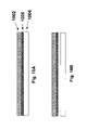
- the carrier may be a solid sheet of material as shown in FIG. 5A , a partial sheet of material as shown in FIG. 5B , or a frame as shown in FIGS. 5C and 5D .
- Useful carrier materials include stainless steel, glass, metals, plastics, and ceramics.
- the coefficient of thermal expansion (CTE) of the carrier is desirable for the coefficient of thermal expansion (CTE) of the carrier to be equal to or slightly larger than the CTE of the substrate. If the CTE of the carrier and substrate are equal, there will not be any stress during thermal cycling and, in the case of a frame, the tension of the substrate will be maintained during thermal cycling. If the CTE of the carrier is slightly larger than the CTE of the substrate, the substrate will be under tension during thermal cycling, which will prevent the substrate from sagging. Another requirement (if heat is used to form the bond between the carrier and the substrate) is that the bond temperature exceed the process temperature (T bond >>T process ) so that the bond remains intact during processing.
- FIG. 7 One preferred embodiment of the method shown in FIG. 6 is illustrated in FIG. 7 .
- a stainless steel substrate 702 is used with a pre-patterned sheet 706 of aluminum as the bonding material and a stainless steel frame 704 as the carrier, this frame is arranged, by engineering of its steel composition, to have a CTE slightly greater than that of the stainless steel substrate. Bonding is effected at approximately 650° C. under pressure.
- the substrate may be released before display dicing or the displays may be diced without debonding the substrate, as described above with reference to FIGS. 2 to 4 . In both cases, it is preferable to clean the frame and reuse it.
- Debonding may be performed by any convenient method, for example elevated temperature, chemical etching, or ultraviolet exposure.
- FIG. 8 shows one example of a carrier 804 that physically holds a substrate 802 .
- the carrier 804 is provided with four upstanding projections 806 and the substrate 802 is provided with corresponding apertures 808 which can be receive these projections 806 .
- This carrier 804 may also be used to tension the substrate 802 if the apertures 808 in the substrate 802 are arranged slightly closer together than the projections 806 on the carrier 804 . Any convenient form of fastener could also be used in the place of the projections/apertures arrangement. Note that in the specific embodiment shown in FIG.
- the projections 806 will extend above the plane of the substrate 802 , and the resultant protrusion may cause problems during processing. Liquid could also get trapped in the fixturing mechanism or between the substrate and carrier.
- the alternative embodiment shown in FIG. 9 in which projections 906 extend diagonally upwardly from the edges of a domed carrier 904 , and can be inserted into apertures (not shown) provided in the peripheral portions of a substrate 902 , these peripheral portions being bent downwardly over the edges of the domed carrier 904 ) does not have any part of the fixture extending above the plane of the substrate 902 , and may thus be preferred.
- the substrate could be diced to produce individual displays without separating it from the carrier. If the substrate is clamped to the carrier or otherwise physically secured, the substrate would normally be removed from the carrier prior to the dicing step.
- an adhesive layer 1006 typically of polyimide or other polymer, is used to secure a steel (or other metal) substrate 1002 to a glass or other rigid carrier 1004 .
- TFT's are formed on the exposed surface (the upper surface in FIG. 10A ) of the steel substrate 1002 using the techniques described above and below, and thereafter the steel substrate 1002 is separated from the carrier 1004 by application of radiation through the carrier, as illustrated in FIG. 10B .
- This process maintains the mechanical advantages of a steel substrate (as opposed to attempting to handle an extremely fragile polymer foil separate from a steel substrate).
- Delamination can also be accomplished using a wet chemical process if the adhesive layer is soluble in the chemical.
- This technique desirably requires a method for delivering the chemical over the entire area rather than just at the edges.
- One approach is to machine holes or channels in the carrier to assist with chemical delivery.
- Another option is to use a porous substrate material or a porous bonding material to assist with chemical delivery.
- Another technique for separating the substrate from the carrier is to use heat (a temperature close to the glass transition temperature of the adhesive layer) to weaken the adhesive-carrier interface.
- the substrate could then be peeled from the carrier.
- a precision tool (such as a wedge) could also be used to separate the substrate from the carrier.
- stainless steel substrates are magnetic or magnetizable, they can be transported and fixtured during the TFT fabrication process by the use of magnets.
- the rigid carrier process of the invention may be carried out by forming the TFT's on a thick, semi-rigid material, for example a polymer, and then back-lapping or thinning the substrate after TFT formation. Such thinning could be effected before or after separation of the individual displays from the process sheet.
- a thick, semi-rigid material for example a polymer
- This invention provides a process for forming a transistor array on an insulating substrate; this process may use only three mask steps.
- an insulating layer substrate is provided.
- a preferred substrate is preferred by depositing an insulating layer 1102 , for example of polyimide (see the aforementioned 2002/0019081) is deposited on to a steel or similar foil 1104 and a passivating layer 1106 , for example of silicon nitride, is deposited over the insulating layer 1104 .
- a first metal layer is coated over the passivating layer 1106 and patterned to form a gate electrode 1108 .
- a gate dielectric layer 1110 typically of silicon nitride
- a semiconductor layer 1112 preferably comprising a layer of amorphous silicon, ⁇ -Si, followed by a layer of n-doped amorphous silicon, n+ ⁇ -Si
- a second metal layer 1114 preferably of aluminum, copper, magnesium, magnesium, magnesium, and magnesium.
- the resultant structure is then etched, preferably by reactive ion etching (RIE) through the full thickness of the second metal layer 1114 and part way through the semiconductor layer 1112 (preferably using a time etch which etches through the n+ ⁇ -Si layer but not through the underlying ⁇ -Si layer; it is of course essential that this ⁇ -Si layer remain within the channel region of the transistor), to produce the structure shown in FIG. 13 , in which the large remaining portion of the second metal layer forms both the source 1116 and drain electrodes 1118 of the transistor and the pixel electrode 1120 which will, in the final form of the display in which the transistor is intended to be used, lie adjacent an electro-optic medium (not shown).
- RIE reactive ion etching
- the semiconductor layer 1112 is continuous between adjacent transistors and thus, as indicated in FIG. 14 , provides a leakage path 1122 between adjacent transistors.
- a second passivating layer 1124 preferably of silicon nitride, is deposited over the whole surface of the substrate to produce the structure shown in FIG. 14 , and thereafter a layer of photoresist (or other etch-resistant material, for example polyimide) is applied and patterned so that the remaining portion 1126 ( FIG. 15 ) of the photoresist covers the portions of the second passivating layer 1124 overlying the source 1116 and drain 1118 electrodes.
- the assembly is subjected to a second etching step, again preferably using reactive ion etching, to produce the structure shown in FIG. 15 ; note that this second etching step uses both the photoresist 1126 and the pixel electrode 1120 as a mask, and etches completely through the semiconductor layer 1112 , thus closing the leakage path 1122 through this layer and completely isolating adjacent transistors from each other.
- the second etching step is illustrated in FIG. 15 as etching completely through the gate dielectric layer 1110 , those skilled in the art of fabricating TFT's will appreciate that this is not strictly necessary and that none, part or all of the thickness of the gate dielectric layer 1110 may be removed during this second etching step.
- the photoresist 1126 or other etch-resistant material shown in FIG. 15 may be removed, or allowed to remain to act as a light shield to reduce light-induced leakage through the channel region of the TFT.
- FIGS. 16 and 17 illustrate two optional additional steps in the process.
- the photoresist may be reflowed by heating as shown in FIG. 16 so that it flows into the gaps 1128 ( FIG. 15 ) provided by the preceding etching step.
- a further layer of conductive material 1130 FIG. 17 , which may be a metal or a conductive polymer may be formed on top of the original pixel electrode 1120 , and this additional conductive layer can extend over the transistor, thus providing a “buried transistor” design.
- contact pads may be formed on the substrate at the same time as, but spaced from, the gate electrodes 1108 , these contact pads being positioned such that the final etching step exposes the contact pads, thus rendering them available for connection to other parts of the overall display.
- the second passivating layer 1124 may be omitted.
- This process of this invention achieves a patterned semiconductor layer without an additional mask step and thus, as compared with prior art processes which do not pattern the semiconductor layer, reduces the degradation of performance caused by leakage through an unpatterned semiconductor layer when the transistor array is in use.
- the cost of backplanes may be significantly reduced by replacing photolithography with printing, and this aspect of the present invention relates to incorporating printing into the manufacture of diode matrix backplanes.
- Printing may be incorporated into electro-optic (especially encapsulated electrophoretic) displays because the electro-optic medium does not require a planar surface, in contrast to liquid crystal displays, which require tight control of cell gaps on the order of 5–10 ⁇ m.
- Printed films are usually on the order of 5–25 ⁇ m so printing is not suitable for liquid crystal displays.
- the performance of printed devices is typically worse than the performance of devices fabricated using standard techniques (photolithography for example).
- encapsulated electrophoretic and some other electro-optic media do not require high drive current and may be able to tolerate the lower performance.
- Metal-insulator metal (MIM) diodes are commonly used for active matrix backplanes.
- the insulator is typically formed by anodizing a patterned metal film.
- a contact hole is formed using photolithography and etching.
- a conductive material such as carbon ink may be screen-printed onto the metal prior to anodization.
- the printed material should be resistant to anodization.
- This invention provides a diode array in which a conductive material is printed on a metal film to eliminate the need for a contact hole later in the process.
- Applicable printing processes include screen, ink-jet, offset, intaglio, gravure, and flexographic (or any combination of these techniques).
- Applicable materials include, but are not limited to, composite materials (screen-printing inks) and organic conductors.
- the diode fabrication process may also be simplified by using a printed dielectric as an etch mask.
- the printed dielectric may remain on the device for isolation and capacitance reduction.
- This invention provides a process for forming a diode on a substrate; in this process, a printed dielectric is used as an etch mask.
- Applicable materials include both organic and inorganic dielectrics, as well as organic/inorganic composites.
- the diode fabrication process may also be simplified by printing one of the electrodes of the diode or the pixel electrode.
- the top electrode and pixel electrode may be printed at the same time.
- the electrode may consist of a multilayer stack.
- the conductive material would be printed onto a thin metal film which provides a high quality interface to the diode.
- the printed material would serve as a mask for etching the thin metal film.
- This invention provides a diode structure in which an electrode can be printed using a conductive material.
- a diode In order to improve the optical performance of a display, it may be desirable to bury the diode and select lines under a printed dielectric.
- the pixel electrode (which may also be printed) would be tied to the diode through a via in the dielectric. This structure ensures that the electronic ink is only driven by the pixel electrode. Again, a printed dielectric is not practical for liquid crystal displays because of the thickness of printed materials. Using standard processes (photolithography and etching) to achieve a buried structure adds cost and complexity which defeats the purpose of using diodes in the first place (low cost, simplified fabrication).
- This invention provides a diode structure in which the diode can be buried using a printed dielectric and printed pixel electrode.
- FIGS. 18A–18D , 19 and 20 of the accompanying drawings illustrate a preferred process of the present invention for formation of diodes.
- a metal layer 1802 is deposited over an insulating substrate, which may be of the polyimide-over-steel type described above and comprise a polyimide layer 1804 formed on a steel substrate 1806 .
- a conductive material 1808 is printed in pad regions and a dielectric material 1810 is printed in a line pattern. (the conductive material 1808 is omitted from FIGS. 18B–18D for ease of illustration). (It will be appreciated that FIGS.
- FIGS. 19 and 20 only illustrate one half of the area shown in FIGS. 19 and 20 , illustrating a single area of dielectric material 1810 and its associated pixel electrode 1814 .
- the next step of the process shown in FIG. 18C , etches the metal layer 1802 using the dielectric 1810 and conductive materials 1808 as a mask, and then anodizes the side walls of the resultant metal strips 1812 .
- a further (optional) metal layer is deposited, a conductive material is printed in the pattern required for pixel electrodes 1814 , and the metal layer (if present) is etched using the printed conductive material as a mask.
- FIG. 21 of the accompanying drawings illustrates one way in which a printed dielectric 2102 and a printed pixel electrode 2104 may be used with a diode 2106 having a top electrode 2108 to provide a buried diode structure.
- electro-optic displays notably electrophoretic, rotating bichromal member and electrochromic displays
- One manner of achieving intermediate optical states is to modulate the impulse seen by the display by using discrete voltage values, time values, or a combination of both.
- the data drivers also called column drivers
- required to provide these many impulse levels can be expensive, especially if they require high voltages, and the cost increases with the number of voltage/time steps required.
- One method of maximizing access to small voltage steps while maintaining high voltage resolution between steps is to provide a band of voltage steps with an offset. For example, one could have 64 levels of voltage available, but instead of having those levels from 0–5V, one could have them from 10–15V.
- the problem is that for a given number of voltage levels and time steps, there are a finite mesh of voltage-time values that can be achieved. If there are desired optical states that cannot be addressed with these values, then those states cannot be displayed.
- This invention provides additional voltage-time states that allow access to “forbidden” states described above.
- the invention is described by means of the following example.
- v-t values is from 1 volt-second to 5.2 volt seconds. If one requires a smaller (or larger) impulse, the values are not available. However if one adds in a discrete voltage value, one achieves four additional v-t states.
- the reference voltages may be formed from a resistor network.
- This invention allows one to eliminate blind spots in the v-t matrix without the addition of more bits of voltage modulation, which is expensive. Instead, one creates a single additional state separated from the closely spaced voltage modulation group to fill in a series of values unreachable with the voltage modulation group alone.
- Electrophoretic and other electro-optic materials require precise control of impulse values to achieve gray levels. Cost efficiency dictates that one cannot provide a continuous set of small steps from 0 to maximum switching voltage, but only use values near the maximum. However, this does not allow one to achieve all of the voltage levels needed for the display of 4-bit grayscale. This simple modification to the driver allows these states to be reached.
Landscapes
- Engineering & Computer Science (AREA)
- Physics & Mathematics (AREA)
- Power Engineering (AREA)
- Microelectronics & Electronic Packaging (AREA)
- General Physics & Mathematics (AREA)
- Computer Hardware Design (AREA)
- Condensed Matter Physics & Semiconductors (AREA)
- Nonlinear Science (AREA)
- Manufacturing & Machinery (AREA)
- Chemical & Material Sciences (AREA)
- Optics & Photonics (AREA)
- Ceramic Engineering (AREA)
- Crystallography & Structural Chemistry (AREA)
- Mathematical Physics (AREA)
- Health & Medical Sciences (AREA)
- Life Sciences & Earth Sciences (AREA)
- Chemical Kinetics & Catalysis (AREA)
- Electrochemistry (AREA)
- Molecular Biology (AREA)
- Mechanical Engineering (AREA)
- Electrochromic Elements, Electrophoresis, Or Variable Reflection Or Absorption Elements (AREA)
- Devices For Indicating Variable Information By Combining Individual Elements (AREA)
Abstract
Description
| time (s) | |||
| voltage (v) | 0.1 | 0.2 | 0.3 | 0.4 |
| 10 | 1.0 | 2.0 | 3.0 | 4.0 |
| 11 | 1.1 | 2.2 | 3.3 | 4.4 |
| 12 | 1.2 | 2.4 | 3.6 | 4.8 |
| 13 | 1.3 | 2.6 | 3.9 | 5.2 |
| time (s) | |||
| voltage (v) | 0.1 | 0.2 | 0.3 | 0.4 |
| 3 | 0.3 | 0.6 | 0.9 | 1.2 |
| 10 | 1.0 | 2.0 | 3.0 | 4.0 |
| 11 | 1.1 | 2.2 | 3.3 | 4.4 |
| 12 | 1.2 | 2.4 | 3.6 | 4.8 |
| 13 | 1.3 | 2.6 | 3.9 | 5.2 |
Claims (24)
Priority Applications (4)
| Application Number | Priority Date | Filing Date | Title |
|---|---|---|---|
| US10/249,624 US7223672B2 (en) | 2002-04-24 | 2003-04-24 | Processes for forming backplanes for electro-optic displays |
| US11/424,258 US7442587B2 (en) | 2002-04-24 | 2006-06-15 | Processes for forming backplanes for electro-optic displays |
| US12/243,411 US7785988B2 (en) | 2002-04-24 | 2008-10-01 | Processes for forming backplanes for electro-optic displays |
| US12/825,991 US8389381B2 (en) | 2002-04-24 | 2010-06-29 | Processes for forming backplanes for electro-optic displays |
Applications Claiming Priority (3)
| Application Number | Priority Date | Filing Date | Title |
|---|---|---|---|
| US37524602P | 2002-04-24 | 2002-04-24 | |
| US37660302P | 2002-04-30 | 2002-04-30 | |
| US10/249,624 US7223672B2 (en) | 2002-04-24 | 2003-04-24 | Processes for forming backplanes for electro-optic displays |
Related Child Applications (1)
| Application Number | Title | Priority Date | Filing Date |
|---|---|---|---|
| US11/424,258 Division US7442587B2 (en) | 2002-04-24 | 2006-06-15 | Processes for forming backplanes for electro-optic displays |
Publications (2)
| Publication Number | Publication Date |
|---|---|
| US20040014265A1 US20040014265A1 (en) | 2004-01-22 |
| US7223672B2 true US7223672B2 (en) | 2007-05-29 |
Family
ID=33492726
Family Applications (4)
| Application Number | Title | Priority Date | Filing Date |
|---|---|---|---|
| US10/249,624 Expired - Lifetime US7223672B2 (en) | 2002-04-24 | 2003-04-24 | Processes for forming backplanes for electro-optic displays |
| US11/424,258 Expired - Fee Related US7442587B2 (en) | 2002-04-24 | 2006-06-15 | Processes for forming backplanes for electro-optic displays |
| US12/243,411 Expired - Fee Related US7785988B2 (en) | 2002-04-24 | 2008-10-01 | Processes for forming backplanes for electro-optic displays |
| US12/825,991 Expired - Lifetime US8389381B2 (en) | 2002-04-24 | 2010-06-29 | Processes for forming backplanes for electro-optic displays |
Family Applications After (3)
| Application Number | Title | Priority Date | Filing Date |
|---|---|---|---|
| US11/424,258 Expired - Fee Related US7442587B2 (en) | 2002-04-24 | 2006-06-15 | Processes for forming backplanes for electro-optic displays |
| US12/243,411 Expired - Fee Related US7785988B2 (en) | 2002-04-24 | 2008-10-01 | Processes for forming backplanes for electro-optic displays |
| US12/825,991 Expired - Lifetime US8389381B2 (en) | 2002-04-24 | 2010-06-29 | Processes for forming backplanes for electro-optic displays |
Country Status (1)
| Country | Link |
|---|---|
| US (4) | US7223672B2 (en) |
Cited By (112)
| Publication number | Priority date | Publication date | Assignee | Title |
|---|---|---|---|---|
| US20040108504A1 (en) * | 2002-11-20 | 2004-06-10 | Charles Forbes | Active matrix thin film transistor array backplane |
| US20050106839A1 (en) * | 2001-07-24 | 2005-05-19 | Seiko Epson Corporation | Transfer method, method of manufacturing thin film devices, method of maufacturing integrated circuits, circuit board and manufacturing method thereof, electro-optical apparatus and manufacturing method thereof, IC card, and electronic appliance |
| US20060199088A1 (en) * | 2005-03-04 | 2006-09-07 | Eastman Kodak Company | Laser etched fiducials in roll-roll display |
| US20070054440A1 (en) * | 2005-09-13 | 2007-03-08 | Tarng-Shiang Hu | Method for fabricating a device with flexible substrate and method for stripping flexible-substrate |
| US20070091417A1 (en) * | 2005-10-25 | 2007-04-26 | E Ink Corporation | Electrophoretic media and displays with improved binder |
| US20070223079A1 (en) * | 2006-03-22 | 2007-09-27 | E Ink Corporation | Electro-optic media produced using ink jet printing |
| US20080074730A1 (en) * | 2006-09-22 | 2008-03-27 | E Ink Corporation | Electro-optic display and materials for use therein |
| US20080129667A1 (en) * | 2004-03-31 | 2008-06-05 | E Ink Corporation | Methods for driving electro-optic displays |
| US20090004442A1 (en) * | 2007-06-28 | 2009-01-01 | E Ink Corporation | Processes for the production of electro-optic displays, and color filters for use therein |
| US20090029527A1 (en) * | 2002-04-24 | 2009-01-29 | E Ink Corporation | Processes for forming backplanes for electro-optic displays |
| US20090155963A1 (en) * | 2007-12-12 | 2009-06-18 | Hawkins Gilbert A | Forming thin film transistors using ablative films |
| US20090168067A1 (en) * | 2002-06-10 | 2009-07-02 | E Ink Corporation | Components and methods for use in electro-optic displays |
| US20090231661A1 (en) * | 2005-06-23 | 2009-09-17 | E Ink Corporation | Edge seals for, and processes for assembly of, electro-optic displays |
| US20090246919A1 (en) * | 2005-12-30 | 2009-10-01 | Au Optronics Corporation | Method for manufacturing pixel structure |
| US20100002437A1 (en) * | 2006-11-27 | 2010-01-07 | Avago Technologies Ecbu (Singapore) Pte. Ltd. | Low Profile and High Efficiency Light Device for Backlighting Applications |
| US7649666B2 (en) | 2006-12-07 | 2010-01-19 | E Ink Corporation | Components and methods for use in electro-optic displays |
| US7649674B2 (en) | 2002-06-10 | 2010-01-19 | E Ink Corporation | Electro-optic display with edge seal |
| US7667886B2 (en) | 2007-01-22 | 2010-02-23 | E Ink Corporation | Multi-layer sheet for use in electro-optic displays |
| US7672040B2 (en) | 2003-11-05 | 2010-03-02 | E Ink Corporation | Electro-optic displays, and materials for use therein |
| US7679814B2 (en) | 2001-04-02 | 2010-03-16 | E Ink Corporation | Materials for use in electrophoretic displays |
| US7688497B2 (en) | 2007-01-22 | 2010-03-30 | E Ink Corporation | Multi-layer sheet for use in electro-optic displays |
| US7733554B2 (en) | 2006-03-08 | 2010-06-08 | E Ink Corporation | Electro-optic displays, and materials and methods for production thereof |
| US7826129B2 (en) | 2007-03-06 | 2010-11-02 | E Ink Corporation | Materials for use in electrophoretic displays |
| US7839564B2 (en) | 2002-09-03 | 2010-11-23 | E Ink Corporation | Components and methods for use in electro-optic displays |
| US7843624B2 (en) | 2006-03-08 | 2010-11-30 | E Ink Corporation | Electro-optic displays, and materials and methods for production thereof |
| US7843621B2 (en) | 2002-06-10 | 2010-11-30 | E Ink Corporation | Components and testing methods for use in the production of electro-optic displays |
| US7843626B2 (en) | 2001-07-09 | 2010-11-30 | E Ink Corporation | Electro-optic display and materials for use therein |
| US7848006B2 (en) | 1995-07-20 | 2010-12-07 | E Ink Corporation | Electrophoretic displays with controlled amounts of pigment |
| US7903319B2 (en) | 2006-07-11 | 2011-03-08 | E Ink Corporation | Electrophoretic medium and display with improved image stability |
| US7910175B2 (en) | 2003-03-25 | 2011-03-22 | E Ink Corporation | Processes for the production of electrophoretic displays |
| US7986450B2 (en) | 2006-09-22 | 2011-07-26 | E Ink Corporation | Electro-optic display and materials for use therein |
| US7999787B2 (en) | 1995-07-20 | 2011-08-16 | E Ink Corporation | Methods for driving electrophoretic displays using dielectrophoretic forces |
| US8018640B2 (en) | 2006-07-13 | 2011-09-13 | E Ink Corporation | Particles for use in electrophoretic displays |
| US8034209B2 (en) | 2007-06-29 | 2011-10-11 | E Ink Corporation | Electro-optic displays, and materials and methods for production thereof |
| US8040594B2 (en) | 1997-08-28 | 2011-10-18 | E Ink Corporation | Multi-color electrophoretic displays |
| US8049947B2 (en) | 2002-06-10 | 2011-11-01 | E Ink Corporation | Components and methods for use in electro-optic displays |
| US8054526B2 (en) | 2008-03-21 | 2011-11-08 | E Ink Corporation | Electro-optic displays, and color filters for use therein |
| US8098418B2 (en) | 2009-03-03 | 2012-01-17 | E. Ink Corporation | Electro-optic displays, and color filters for use therein |
| US8115729B2 (en) | 1999-05-03 | 2012-02-14 | E Ink Corporation | Electrophoretic display element with filler particles |
| US8177942B2 (en) | 2003-11-05 | 2012-05-15 | E Ink Corporation | Electro-optic displays, and materials for use therein |
| US8234507B2 (en) | 2009-01-13 | 2012-07-31 | Metrologic Instruments, Inc. | Electronic-ink display device employing a power switching mechanism automatically responsive to predefined states of device configuration |
| US8270064B2 (en) | 2009-02-09 | 2012-09-18 | E Ink Corporation | Electrophoretic particles, and processes for the production thereof |
| US8305341B2 (en) | 1995-07-20 | 2012-11-06 | E Ink Corporation | Dielectrophoretic displays |
| US8314784B2 (en) | 2008-04-11 | 2012-11-20 | E Ink Corporation | Methods for driving electro-optic displays |
| US20130003162A1 (en) * | 2011-06-29 | 2013-01-03 | Napoleon Leoni | Electronic paper with porous standoff layer |
| US8363299B2 (en) | 2002-06-10 | 2013-01-29 | E Ink Corporation | Electro-optic displays, and processes for the production thereof |
| EP2555182A1 (en) | 2007-02-02 | 2013-02-06 | E Ink Corporation | Electrophoretic displays having transparent electrode and conductor connected thereto |
| US8390301B2 (en) | 2006-03-08 | 2013-03-05 | E Ink Corporation | Electro-optic displays, and materials and methods for production thereof |
| US8390918B2 (en) | 2001-04-02 | 2013-03-05 | E Ink Corporation | Electrophoretic displays with controlled amounts of pigment |
| US8446664B2 (en) | 2010-04-02 | 2013-05-21 | E Ink Corporation | Electrophoretic media, and materials for use therein |
| US8457013B2 (en) | 2009-01-13 | 2013-06-04 | Metrologic Instruments, Inc. | Wireless dual-function network device dynamically switching and reconfiguring from a wireless network router state of operation into a wireless network coordinator state of operation in a wireless communication network |
| US8553012B2 (en) | 2001-03-13 | 2013-10-08 | E Ink Corporation | Apparatus for displaying drawings |
| US8610988B2 (en) | 2006-03-09 | 2013-12-17 | E Ink Corporation | Electro-optic display with edge seal |
| US8654436B1 (en) | 2009-10-30 | 2014-02-18 | E Ink Corporation | Particles for use in electrophoretic displays |
| US8754859B2 (en) | 2009-10-28 | 2014-06-17 | E Ink Corporation | Electro-optic displays with touch sensors and/or tactile feedback |
| US8902153B2 (en) | 2007-08-03 | 2014-12-02 | E Ink Corporation | Electro-optic displays, and processes for their production |
| US9023448B2 (en) | 2013-02-22 | 2015-05-05 | Industrial Technology Research Institute | Substrate structures applied in flexible devices |
| US9170467B2 (en) | 2005-10-18 | 2015-10-27 | E Ink Corporation | Color electro-optic displays, and processes for the production thereof |
| US9269311B2 (en) | 2001-11-20 | 2016-02-23 | E Ink Corporation | Methods and apparatus for driving electro-optic displays |
| US9293511B2 (en) | 1998-07-08 | 2016-03-22 | E Ink Corporation | Methods for achieving improved color in microencapsulated electrophoretic devices |
| US9412314B2 (en) | 2001-11-20 | 2016-08-09 | E Ink Corporation | Methods for driving electro-optic displays |
| US9470950B2 (en) | 2002-06-10 | 2016-10-18 | E Ink Corporation | Electro-optic displays, and processes for the production thereof |
| WO2016191673A1 (en) | 2015-05-27 | 2016-12-01 | E Ink Corporation | Methods and circuitry for driving display devices |
| US9530363B2 (en) | 2001-11-20 | 2016-12-27 | E Ink Corporation | Methods and apparatus for driving electro-optic displays |
| US9529240B2 (en) | 2014-01-17 | 2016-12-27 | E Ink Corporation | Controlled polymeric material conductivity for use in a two-phase electrode layer |
| US9564088B2 (en) | 2001-11-20 | 2017-02-07 | E Ink Corporation | Electro-optic displays with reduced remnant voltage |
| US9620067B2 (en) | 2003-03-31 | 2017-04-11 | E Ink Corporation | Methods for driving electro-optic displays |
| US9664978B2 (en) | 2002-10-16 | 2017-05-30 | E Ink Corporation | Electrophoretic displays |
| US9671635B2 (en) | 2014-02-07 | 2017-06-06 | E Ink Corporation | Electro-optic display backplane structures with drive components and pixel electrodes on opposed surfaces |
| US9715155B1 (en) | 2013-01-10 | 2017-07-25 | E Ink Corporation | Electrode structures for electro-optic displays |
| US9726957B2 (en) | 2013-01-10 | 2017-08-08 | E Ink Corporation | Electro-optic display with controlled electrochemical reactions |
| US9835925B1 (en) | 2015-01-08 | 2017-12-05 | E Ink Corporation | Electro-optic displays, and processes for the production thereof |
| US9847243B2 (en) | 2009-08-27 | 2017-12-19 | Corning Incorporated | Debonding a glass substrate from carrier using ultrasonic wave |
| US9964831B2 (en) | 2007-11-14 | 2018-05-08 | E Ink Corporation | Electro-optic assemblies, and adhesives and binders for use therein |
| WO2018102126A1 (en) | 2016-11-30 | 2018-06-07 | E Ink Corporation | Laminated electro-optic displays and methods of making the same |
| US10048564B2 (en) | 2003-11-05 | 2018-08-14 | E Ink Corporation | Electro-optic displays, and materials for use therein |
| US10175550B2 (en) | 2014-11-07 | 2019-01-08 | E Ink Corporation | Applications of electro-optic displays |
| US10190743B2 (en) | 2012-04-20 | 2019-01-29 | E Ink Corporation | Illumination systems for reflective displays |
| WO2019089042A1 (en) | 2017-11-03 | 2019-05-09 | E Ink Corporation | Processes for producing electro-optic displays |
| US10319313B2 (en) | 2007-05-21 | 2019-06-11 | E Ink Corporation | Methods for driving video electro-optic displays |
| US10317767B2 (en) | 2014-02-07 | 2019-06-11 | E Ink Corporation | Electro-optic display backplane structure with drive components and pixel electrodes on opposed surfaces |
| US10319314B2 (en) | 1999-04-30 | 2019-06-11 | E Ink Corporation | Methods for driving electro-optic displays, and apparatus for use therein |
| US10324577B2 (en) | 2017-02-28 | 2019-06-18 | E Ink Corporation | Writeable electrophoretic displays including sensing circuits and styli configured to interact with sensing circuits |
| US10446585B2 (en) | 2014-03-17 | 2019-10-15 | E Ink Corporation | Multi-layer expanding electrode structures for backplane assemblies |
| US10444590B2 (en) | 2002-09-03 | 2019-10-15 | E Ink Corporation | Electro-optic displays |
| US10466565B2 (en) | 2017-03-28 | 2019-11-05 | E Ink Corporation | Porous backplane for electro-optic display |
| US10475396B2 (en) | 2015-02-04 | 2019-11-12 | E Ink Corporation | Electro-optic displays with reduced remnant voltage, and related apparatus and methods |
| US10495941B2 (en) | 2017-05-19 | 2019-12-03 | E Ink Corporation | Foldable electro-optic display including digitization and touch sensing |
| US10527899B2 (en) | 2016-05-31 | 2020-01-07 | E Ink Corporation | Backplanes for electro-optic displays |
| US10538111B2 (en) | 2010-06-02 | 2020-01-21 | Hewlett-Packard Development Company, L.P. | Writing electronic paper |
| US10573257B2 (en) | 2017-05-30 | 2020-02-25 | E Ink Corporation | Electro-optic displays |
| WO2020060960A1 (en) | 2018-09-17 | 2020-03-26 | E Ink Corporation | Backplanes with hexagonal and triangular electrodes |
| WO2020097462A1 (en) | 2018-11-09 | 2020-05-14 | E Ink Corporation | Electro-optic displays |
| WO2020122917A1 (en) | 2018-12-13 | 2020-06-18 | E Ink Corporation | Illumination systems for reflective displays |
| US10726798B2 (en) | 2003-03-31 | 2020-07-28 | E Ink Corporation | Methods for operating electro-optic displays |
| US10824042B1 (en) | 2017-10-27 | 2020-11-03 | E Ink Corporation | Electro-optic display and composite materials having low thermal sensitivity for use therein |
| US10882042B2 (en) | 2017-10-18 | 2021-01-05 | E Ink Corporation | Digital microfluidic devices including dual substrates with thin-film transistors and capacitive sensing |
| US11081066B2 (en) | 2018-02-15 | 2021-08-03 | E Ink Corporation | Via placement for slim border electro-optic display backplanes with decreased capacitive coupling between t-wires and pixel electrodes |
| US11175561B1 (en) | 2018-04-12 | 2021-11-16 | E Ink Corporation | Electrophoretic display media with network electrodes and methods of making and using the same |
| US11250794B2 (en) | 2004-07-27 | 2022-02-15 | E Ink Corporation | Methods for driving electrophoretic displays using dielectrophoretic forces |
| US11397361B2 (en) | 2015-06-29 | 2022-07-26 | E Ink Corporation | Method for mechanical and electrical connection to display electrodes |
| US11404013B2 (en) | 2017-05-30 | 2022-08-02 | E Ink Corporation | Electro-optic displays with resistors for discharging remnant charges |
| US11467466B2 (en) | 2012-04-20 | 2022-10-11 | E Ink Corporation | Illumination systems for reflective displays |
| US11511096B2 (en) | 2018-10-15 | 2022-11-29 | E Ink Corporation | Digital microfluidic delivery device |
| US11513415B2 (en) | 2020-06-03 | 2022-11-29 | E Ink Corporation | Foldable electrophoretic display module including non-conductive support plate |
| US11521565B2 (en) | 2018-12-28 | 2022-12-06 | E Ink Corporation | Crosstalk reduction for electro-optic displays |
| US11537024B2 (en) | 2018-12-30 | 2022-12-27 | E Ink California, Llc | Electro-optic displays |
| US11644732B2 (en) | 2014-01-31 | 2023-05-09 | Hewlett-Packard Development Company, L.P. | Display device |
| US11733580B2 (en) | 2010-05-21 | 2023-08-22 | E Ink Corporation | Method for driving two layer variable transmission display |
| WO2023167901A1 (en) | 2022-03-01 | 2023-09-07 | E Ink California, Llc | Temperature compensation in electro-optic displays |
| US11892739B2 (en) | 2020-02-07 | 2024-02-06 | E Ink Corporation | Electrophoretic display layer with thin film top electrode |
| US11935495B2 (en) | 2021-08-18 | 2024-03-19 | E Ink Corporation | Methods for driving electro-optic displays |
Families Citing this family (107)
| Publication number | Priority date | Publication date | Assignee | Title |
|---|---|---|---|---|
| US7411719B2 (en) | 1995-07-20 | 2008-08-12 | E Ink Corporation | Electrophoretic medium and process for the production thereof |
| US8139050B2 (en) * | 1995-07-20 | 2012-03-20 | E Ink Corporation | Addressing schemes for electronic displays |
| US7327511B2 (en) * | 2004-03-23 | 2008-02-05 | E Ink Corporation | Light modulators |
| US7119772B2 (en) * | 1999-04-30 | 2006-10-10 | E Ink Corporation | Methods for driving bistable electro-optic displays, and apparatus for use therein |
| US7119759B2 (en) * | 1999-05-03 | 2006-10-10 | E Ink Corporation | Machine-readable displays |
| US8009348B2 (en) * | 1999-05-03 | 2011-08-30 | E Ink Corporation | Machine-readable displays |
| US20100330748A1 (en) * | 1999-10-25 | 2010-12-30 | Xi Chu | Method of encapsulating an environmentally sensitive device |
| US7893435B2 (en) * | 2000-04-18 | 2011-02-22 | E Ink Corporation | Flexible electronic circuits and displays including a backplane comprising a patterned metal foil having a plurality of apertures extending therethrough |
| US20050156340A1 (en) * | 2004-01-20 | 2005-07-21 | E Ink Corporation | Preparation of capsules |
| US7230750B2 (en) * | 2001-05-15 | 2007-06-12 | E Ink Corporation | Electrophoretic media and processes for the production thereof |
| US7110163B2 (en) * | 2001-07-09 | 2006-09-19 | E Ink Corporation | Electro-optic display and lamination adhesive for use therein |
| US7528822B2 (en) * | 2001-11-20 | 2009-05-05 | E Ink Corporation | Methods for driving electro-optic displays |
| US8125501B2 (en) | 2001-11-20 | 2012-02-28 | E Ink Corporation | Voltage modulated driver circuits for electro-optic displays |
| US7952557B2 (en) * | 2001-11-20 | 2011-05-31 | E Ink Corporation | Methods and apparatus for driving electro-optic displays |
| US8808457B2 (en) | 2002-04-15 | 2014-08-19 | Samsung Display Co., Ltd. | Apparatus for depositing a multilayer coating on discrete sheets |
| US7190008B2 (en) * | 2002-04-24 | 2007-03-13 | E Ink Corporation | Electro-optic displays, and components for use therein |
| KR100896167B1 (en) * | 2002-04-24 | 2009-05-11 | 이 잉크 코포레이션 | Electronic displays |
| US6958848B2 (en) * | 2002-05-23 | 2005-10-25 | E Ink Corporation | Capsules, materials for use therein and electrophoretic media and displays containing such capsules |
| US7110164B2 (en) * | 2002-06-10 | 2006-09-19 | E Ink Corporation | Electro-optic displays, and processes for the production thereof |
| US20110199671A1 (en) * | 2002-06-13 | 2011-08-18 | E Ink Corporation | Methods for driving electrophoretic displays using dielectrophoretic forces |
| US20080024482A1 (en) | 2002-06-13 | 2008-01-31 | E Ink Corporation | Methods for driving electro-optic displays |
| US20040105036A1 (en) * | 2002-08-06 | 2004-06-03 | E Ink Corporation | Protection of electro-optic displays against thermal effects |
| US7312916B2 (en) * | 2002-08-07 | 2007-12-25 | E Ink Corporation | Electrophoretic media containing specularly reflective particles |
| US8129655B2 (en) | 2002-09-03 | 2012-03-06 | E Ink Corporation | Electrophoretic medium with gaseous suspending fluid |
| CN1726428A (en) * | 2002-12-16 | 2006-01-25 | 伊英克公司 | Backplanes for electro-optic displays |
| US6987603B2 (en) * | 2003-01-31 | 2006-01-17 | E Ink Corporation | Construction of electrophoretic displays |
| US7339715B2 (en) * | 2003-03-25 | 2008-03-04 | E Ink Corporation | Processes for the production of electrophoretic displays |
| WO2004088395A2 (en) * | 2003-03-27 | 2004-10-14 | E Ink Corporation | Electro-optic assemblies |
| WO2004099862A2 (en) * | 2003-05-02 | 2004-11-18 | E Ink Corporation | Electrophoretic displays |
| JP5904690B2 (en) | 2003-06-30 | 2016-04-20 | イー インク コーポレイション | Method for driving an electro-optic display |
| US8174490B2 (en) * | 2003-06-30 | 2012-05-08 | E Ink Corporation | Methods for driving electrophoretic displays |
| US20050122563A1 (en) | 2003-07-24 | 2005-06-09 | E Ink Corporation | Electro-optic displays |
| EP2698784B1 (en) | 2003-08-19 | 2017-11-01 | E Ink Corporation | Electro-optic display |
| WO2005029458A1 (en) * | 2003-09-19 | 2005-03-31 | E Ink Corporation | Methods for reducing edge effects in electro-optic displays |
| EP1671304B1 (en) * | 2003-10-08 | 2008-08-20 | E Ink Corporation | Electro-wetting displays |
| US8319759B2 (en) | 2003-10-08 | 2012-11-27 | E Ink Corporation | Electrowetting displays |
| EP2487674B1 (en) | 2003-11-05 | 2018-02-21 | E Ink Corporation | Electro-optic displays |
| US8928562B2 (en) * | 2003-11-25 | 2015-01-06 | E Ink Corporation | Electro-optic displays, and methods for driving same |
| WO2005054933A2 (en) | 2003-11-26 | 2005-06-16 | E Ink Corporation | Electro-optic displays with reduced remnant voltage |
| KR101095293B1 (en) | 2003-11-28 | 2011-12-16 | 가부시키가이샤 한도오따이 에네루기 켄큐쇼 | Method of manufacturing display device |
| US7206119B2 (en) * | 2003-12-31 | 2007-04-17 | E Ink Corporation | Electro-optic displays, and method for driving same |
| US7075703B2 (en) * | 2004-01-16 | 2006-07-11 | E Ink Corporation | Process for sealing electro-optic displays |
| US7388572B2 (en) * | 2004-02-27 | 2008-06-17 | E Ink Corporation | Backplanes for electro-optic displays |
| US7492339B2 (en) * | 2004-03-26 | 2009-02-17 | E Ink Corporation | Methods for driving bistable electro-optic displays |
| US20050253777A1 (en) * | 2004-05-12 | 2005-11-17 | E Ink Corporation | Tiled displays and methods for driving same |
| US20060003485A1 (en) * | 2004-06-30 | 2006-01-05 | Hoffman Randy L | Devices and methods of making the same |
| CN100557474C (en) * | 2004-07-27 | 2009-11-04 | 伊英克公司 | Electro-optic displays |
| US7259106B2 (en) * | 2004-09-10 | 2007-08-21 | Versatilis Llc | Method of making a microelectronic and/or optoelectronic circuitry sheet |
| US7563691B2 (en) * | 2004-10-29 | 2009-07-21 | Hewlett-Packard Development Company, L.P. | Method for plasma enhanced bonding and bonded structures formed by plasma enhanced bonding |
| US20060091496A1 (en) * | 2004-10-28 | 2006-05-04 | Hewlett-Packard Development Company, Lp | Metal-insulator-metal device |
| US7160745B2 (en) * | 2004-10-28 | 2007-01-09 | Hewlett-Packard Development Company, L.P. | Metal-insulator-metal device |
| EP1842093A4 (en) * | 2005-01-26 | 2010-11-24 | E Ink Corp | Electrophoretic displays using gaseous fluids |
| JP2006258883A (en) * | 2005-03-15 | 2006-09-28 | Seiko Epson Corp | Electrooptical device, and manufacturing method for electrooptical device |
| WO2007048096A2 (en) | 2005-10-18 | 2007-04-26 | E Ink Corporation | Components for electro-optic displays |
| KR101095159B1 (en) * | 2006-07-05 | 2011-12-16 | 아리조나 보드 오브 리전트스, 아리조나주의 아리조나 주립대 대행법인 | Method of temporarily attaching a rigid carrier to a substrate |
| US7678701B2 (en) * | 2006-07-31 | 2010-03-16 | Eastman Kodak Company | Flexible substrate with electronic devices formed thereon |
| CN101501832A (en) * | 2006-08-10 | 2009-08-05 | 皇家飞利浦电子股份有限公司 | Active matrix displays and other electronic devices having plastic substrates |
| KR101237262B1 (en) | 2006-09-18 | 2013-02-27 | 이 잉크 코포레이션 | Color electro-optic displays |
| US8077142B2 (en) * | 2006-09-27 | 2011-12-13 | Tred Displays Corporation | Reflective, bi-stable magneto optical display architectures |
| CN100464404C (en) * | 2007-01-30 | 2009-02-25 | 友达光电股份有限公司 | Making method of pixel structure |
| CN100463110C (en) * | 2007-04-06 | 2009-02-18 | 天津中环半导体股份有限公司 | Electrophoresis method glass passivation technology of the silicon rectifier |
| KR20080099541A (en) * | 2007-05-09 | 2008-11-13 | 삼성전자주식회사 | Display device and manufacturing method thereof |
| US20090159176A1 (en) * | 2007-12-21 | 2009-06-25 | Palo Alto Research Center Incorporated | Sealing method for containing materials |
| US20090202857A1 (en) * | 2008-02-08 | 2009-08-13 | Roger Stanley Kerr | Method for forming an electronic device on a flexible metallic substrate and resultant device |
| US20090200543A1 (en) * | 2008-02-08 | 2009-08-13 | Roger Stanley Kerr | Method of forming an electronic device on a substrate supported by a carrier and resultant device |
| KR20090130703A (en) * | 2008-06-16 | 2009-12-24 | 삼성전자주식회사 | Flexible reflective display device |
| SG171917A1 (en) | 2008-12-02 | 2011-07-28 | Univ Arizona | Method of preparing a flexible substrate assembly and flexible substrate assembly therefrom |
| WO2013082138A1 (en) * | 2011-11-29 | 2013-06-06 | Arizona Board Of Regents, A Body Corporate Of The State Of Arizona For And On Behalf Of Arizona State University | Method of providing an electronic device structure and related electronic device structures |
| US9721825B2 (en) | 2008-12-02 | 2017-08-01 | Arizona Board Of Regents, A Body Corporate Of The State Of Arizona, Acting For And On Behalf Of Arizona State University | Method of providing a flexible semiconductor device and flexible semiconductor device thereof |
| US9601530B2 (en) | 2008-12-02 | 2017-03-21 | Arizona Board Of Regents, A Body Corporated Of The State Of Arizona, Acting For And On Behalf Of Arizona State University | Dual active layer semiconductor device and method of manufacturing the same |
| US9991311B2 (en) | 2008-12-02 | 2018-06-05 | Arizona Board Of Regents On Behalf Of Arizona State University | Dual active layer semiconductor device and method of manufacturing the same |
| KR101362025B1 (en) * | 2009-05-29 | 2014-02-13 | 아리조나 보드 오브 리젠츠 퍼 앤 온 비하프 오브 아리조나 스테이트 유니버시티 | Method of providing a flexible semiconductor device at high temperatures and flexible semiconductor device thereof |
| WO2011019429A2 (en) * | 2009-06-09 | 2011-02-17 | Arizona Technology Enterprises | Method of anodizing aluminum using a hard mask and semiconductor device thereof |
| CN102576735B (en) * | 2009-09-30 | 2016-01-20 | 大日本印刷株式会社 | The manufacture method of flexible device substrate, flexible device thin film transistor base plate, flexible device, thin-film component substrate, thin-film component, thin-film transistor, the manufacture method of thin-film component substrate, the manufacture method of thin-film component and thin-film transistor |
| US8590338B2 (en) | 2009-12-31 | 2013-11-26 | Samsung Mobile Display Co., Ltd. | Evaporator with internal restriction |
| WO2012021197A2 (en) * | 2010-05-21 | 2012-02-16 | Arizona Board Of Regents, For And On Behalf Of Arizona State University | Method of manufacturing electronic devices on both sides of a carrier substrate and electronic devices thereof |
| WO2012021196A2 (en) | 2010-05-21 | 2012-02-16 | Arizona Board Of Regents, For And On Behalf Of Arizona State University | Method for manufacturing electronic devices and electronic devices thereof |
| US9846493B2 (en) | 2010-06-02 | 2017-12-19 | Hewlett-Packard Development Company, L.P. | Systems and methods for writing on and using electronic paper |
| KR101783781B1 (en) * | 2010-07-05 | 2017-10-11 | 삼성디스플레이 주식회사 | A flat display device and the manufacturing method thereof |
| KR101852190B1 (en) * | 2011-06-28 | 2018-04-25 | 엘지디스플레이 주식회사 | Manufacturing method of flexible display |
| KR101839453B1 (en) * | 2011-08-02 | 2018-03-16 | 엘지디스플레이 주식회사 | Apparatus and method for manufacturing a flexible display device |
| CN102956550B (en) * | 2011-08-18 | 2015-03-25 | 元太科技工业股份有限公司 | Method for manufacturing active array substrate and active array substrate |
| TWI539414B (en) | 2011-09-21 | 2016-06-21 | 友達光電股份有限公司 | Fabricating method of flexible display |
| US20130125910A1 (en) | 2011-11-18 | 2013-05-23 | Avon Products, Inc. | Use of Electrophoretic Microcapsules in a Cosmetic Composition |
| US10042189B2 (en) | 2011-12-01 | 2018-08-07 | Avery Dennison Retail Information Services, Llc | Backplane for electrophoretic display |
| CA2863425C (en) | 2012-02-01 | 2021-02-16 | E Ink Corporation | Methods for driving electro-optic displays |
| US9366922B2 (en) * | 2012-02-07 | 2016-06-14 | Shenzhen China Star Optoelectronics Technology Co., Ltd. | Thin film transistor array and method for manufacturing the same |
| TWI463235B (en) * | 2012-03-15 | 2014-12-01 | E Ink Holdings Inc | Driving substrate and display using the same |
| KR101960745B1 (en) * | 2012-11-14 | 2019-03-21 | 엘지디스플레이 주식회사 | Method of cutting flexible display device and method of fabricating flexible display device |
| US8659173B1 (en) | 2013-01-04 | 2014-02-25 | International Business Machines Corporation | Isolated wire structures with reduced stress, methods of manufacturing and design structures |
| CN103337500B (en) * | 2013-05-24 | 2015-12-23 | 友达光电股份有限公司 | Active component array base board and manufacture method thereof |
| KR20150001441A (en) * | 2013-06-27 | 2015-01-06 | 삼성디스플레이 주식회사 | Manufacturing method of flexible display device |
| ES2946753T3 (en) | 2013-07-31 | 2023-07-25 | E Ink Corp | Methods for driving electro-optical displays |
| US10381224B2 (en) | 2014-01-23 | 2019-08-13 | Arizona Board Of Regents On Behalf Of Arizona State University | Method of providing an electronic device and electronic device thereof |
| WO2017034645A2 (en) | 2015-06-09 | 2017-03-02 | ARIZONA BOARD OF REGENTS, a body corporate for THE STATE OF ARIZONA for and on behalf of ARIZONA STATE UNIVERSITY | Method of providing an electronic device and electronic device thereof |
| WO2015156891A2 (en) | 2014-01-23 | 2015-10-15 | Arizona Board Of Regents, Acting For And On Behalf Of Arizona State University | Method of providing a flexible semiconductor device and flexible semiconductor device thereof |
| KR102466741B1 (en) | 2014-05-13 | 2022-11-15 | 아리조나 보드 오브 리젠츠 온 비하프 오브 아리조나 스테이트 유니버시티 | Method of providing an electronic device |
| CN104409408B (en) * | 2014-12-02 | 2017-10-10 | 昆山国显光电有限公司 | A kind of preparation method of rigid substrates and flexible display |
| KR102032158B1 (en) | 2014-12-19 | 2019-10-15 | 글로 에이비 | Light emitting diode array on a backplane and method of making thereof |
| US10446582B2 (en) | 2014-12-22 | 2019-10-15 | Arizona Board Of Regents On Behalf Of Arizona State University | Method of providing an imaging system and imaging system thereof |
| US9741742B2 (en) | 2014-12-22 | 2017-08-22 | Arizona Board Of Regents, A Body Corporate Of The State Of Arizona, Acting For And On Behalf Of Arizona State University | Deformable electronic device and methods of providing and using deformable electronic device |
| KR20170010697A (en) * | 2015-07-20 | 2017-02-01 | 재단법인 나노기반소프트일렉트로닉스연구단 | Flexible electronic device having adhesive function and method for manufacturing same |
| US9635764B2 (en) | 2015-09-25 | 2017-04-25 | Intel Corporation | Integrated circuit and method that utilize a shape memory material |
| WO2018204582A1 (en) * | 2017-05-03 | 2018-11-08 | Chromera, Inc. | Electrically determining messages on an electrophoretic display |
| CN114761174A (en) * | 2019-11-25 | 2022-07-15 | 康宁股份有限公司 | Bonded article and method of forming same |
| TW202349091A (en) | 2022-02-25 | 2023-12-16 | 美商電子墨水股份有限公司 | Electro-optic displays with edge seal components and methods of making the same |
| US20230350263A1 (en) | 2022-04-27 | 2023-11-02 | E Ink Corporation | Electro-optic display stacks with segmented electrodes and methods of making the same |
Citations (96)
| Publication number | Priority date | Publication date | Assignee | Title |
|---|---|---|---|---|
| US3668106A (en) | 1970-04-09 | 1972-06-06 | Matsushita Electric Ind Co Ltd | Electrophoretic display device |
| US3756693A (en) | 1970-12-21 | 1973-09-04 | Matsushita Electric Ind Co Ltd | Electrophoretic display device |
| US3767392A (en) | 1970-04-15 | 1973-10-23 | Matsushita Electric Ind Co Ltd | Electrophoretic light image reproduction process |
| US3792308A (en) | 1970-06-08 | 1974-02-12 | Matsushita Electric Ind Co Ltd | Electrophoretic display device of the luminescent type |
| US3870517A (en) | 1969-10-18 | 1975-03-11 | Matsushita Electric Ind Co Ltd | Color image reproduction sheet employed in photoelectrophoretic imaging |
| US3892568A (en) | 1969-04-23 | 1975-07-01 | Matsushita Electric Ind Co Ltd | Electrophoretic image reproduction process |
| US4810637A (en) | 1985-05-07 | 1989-03-07 | Thomson-Csf | Non-linear control element for a flat electrooptical display screen and a method of fabrication of said control element |
| US5175047A (en) | 1990-08-09 | 1992-12-29 | Teledyne Industries, Inc. | Rigid-flex printed circuit |
| US5234541A (en) | 1990-06-04 | 1993-08-10 | U.S. Philips Corporation | Methods of fabricating mim type device arrays and display devices incorporating such arrays |
| US5238861A (en) | 1990-05-15 | 1993-08-24 | France Telecom Etablissement Autonome De Droit Public(Centre National D'etudes Des Telecommunications) | Method for manufacturing an active matrix display screen with storage capacitors |
| US5362671A (en) | 1990-12-31 | 1994-11-08 | Kopin Corporation | Method of fabricating single crystal silicon arrayed devices for display panels |
| US5414283A (en) | 1993-11-19 | 1995-05-09 | Ois Optical Imaging Systems, Inc. | TFT with reduced parasitic capacitance |
| US5569610A (en) | 1993-03-12 | 1996-10-29 | Semiconductor Energy Laboratory Co., Ltd. | Method of manufacturing multiple polysilicon TFTs with varying degrees of crystallinity |
| US5641974A (en) | 1995-06-06 | 1997-06-24 | Ois Optical Imaging Systems, Inc. | LCD with bus lines overlapped by pixel electrodes and photo-imageable insulating layer therebetween |
| US5715026A (en) | 1989-09-15 | 1998-02-03 | U.S. Philips Corporation | Method of fabricating active matrix display devices with prefabricated discrete non-linear devices |
| US5760761A (en) | 1995-12-15 | 1998-06-02 | Xerox Corporation | Highlight color twisting ball display |
| US5777782A (en) | 1996-12-24 | 1998-07-07 | Xerox Corporation | Auxiliary optics for a twisting ball display |
| US5808783A (en) | 1996-06-27 | 1998-09-15 | Xerox Corporation | High reflectance gyricon display |
| US5824186A (en) | 1993-12-17 | 1998-10-20 | The Regents Of The University Of California | Method and apparatus for fabricating self-assembling microstructures |
| US5847413A (en) | 1994-08-31 | 1998-12-08 | Semiconductor Energy Laboratory Co., Ltd. | Differential amplifier circuit and analog buffer |
| US5904545A (en) | 1993-12-17 | 1999-05-18 | The Regents Of The University Of California | Apparatus for fabricating self-assembling microstructures |
| US5930026A (en) | 1996-10-25 | 1999-07-27 | Massachusetts Institute Of Technology | Nonemissive displays and piezoelectric power supplies therefor |
| US5961804A (en) | 1997-03-18 | 1999-10-05 | Massachusetts Institute Of Technology | Microencapsulated electrophoretic display |
| US6017584A (en) | 1995-07-20 | 2000-01-25 | E Ink Corporation | Multi-color electrophoretic displays and materials for making the same |
| US6027958A (en) | 1996-07-11 | 2000-02-22 | Kopin Corporation | Transferred flexible integrated circuit |
| US6054071A (en) | 1998-01-28 | 2000-04-25 | Xerox Corporation | Poled electrets for gyricon-based electric-paper displays |
| US6055091A (en) | 1996-06-27 | 2000-04-25 | Xerox Corporation | Twisting-cylinder display |
| US6067185A (en) | 1997-08-28 | 2000-05-23 | E Ink Corporation | Process for creating an encapsulated electrophoretic display |
| US6097531A (en) | 1998-11-25 | 2000-08-01 | Xerox Corporation | Method of making uniformly magnetized elements for a gyricon display |
| US6118426A (en) | 1995-07-20 | 2000-09-12 | E Ink Corporation | Transducers and indicators having printed displays |
| US6120588A (en) | 1996-07-19 | 2000-09-19 | E Ink Corporation | Electronically addressable microencapsulated ink and display thereof |
| US6120839A (en) | 1995-07-20 | 2000-09-19 | E Ink Corporation | Electro-osmotic displays and materials for making the same |
| US6124851A (en) | 1995-07-20 | 2000-09-26 | E Ink Corporation | Electronic book with multiple page displays |
| US6127199A (en) | 1996-11-12 | 2000-10-03 | Seiko Epson Corporation | Manufacturing method of active matrix substrate, active matrix substrate and liquid crystal display device |
| US6128124A (en) | 1998-10-16 | 2000-10-03 | Xerox Corporation | Additive color electric paper without registration or alignment of individual elements |
| US6130774A (en) | 1998-04-27 | 2000-10-10 | E Ink Corporation | Shutter mode microencapsulated electrophoretic display |
| US6137467A (en) | 1995-01-03 | 2000-10-24 | Xerox Corporation | Optically sensitive electric paper |
| US6147791A (en) | 1998-11-25 | 2000-11-14 | Xerox Corporation | Gyricon displays utilizing rotating elements and magnetic latching |
| US6150668A (en) | 1998-05-29 | 2000-11-21 | Lucent Technologies Inc. | Thin-film transistor monolithically integrated with an organic light-emitting diode |
| US6172878B1 (en) | 1997-12-27 | 2001-01-09 | Canon Kabushiki Kaisha | Multi-element module and production process thereof |
| US6177921B1 (en) | 1997-08-28 | 2001-01-23 | E Ink Corporation | Printable electrode structures for displays |
| US6232950B1 (en) | 1997-08-28 | 2001-05-15 | E Ink Corporation | Rear electrode structures for displays |
| US6249271B1 (en) | 1995-07-20 | 2001-06-19 | E Ink Corporation | Retroreflective electrophoretic displays and materials for making the same |
| US6252564B1 (en) | 1997-08-28 | 2001-06-26 | E Ink Corporation | Tiled displays |
| US6262833B1 (en) | 1998-10-07 | 2001-07-17 | E Ink Corporation | Capsules for electrophoretic displays and methods for making the same |
| US6262706B1 (en) | 1995-07-20 | 2001-07-17 | E Ink Corporation | Retroreflective electrophoretic displays and materials for making the same |
| US6274412B1 (en) | 1998-12-21 | 2001-08-14 | Parelec, Inc. | Material and method for printing high conductivity electrical conductors and other components on thin film transistor arrays |
| US6301038B1 (en) | 1997-02-06 | 2001-10-09 | University College Dublin | Electrochromic system |
| US6300932B1 (en) | 1997-08-28 | 2001-10-09 | E Ink Corporation | Electrophoretic displays with luminescent particles and materials for making the same |
| US6312304B1 (en) | 1998-12-15 | 2001-11-06 | E Ink Corporation | Assembly of microencapsulated electronic displays |
| US6312971B1 (en) | 1999-08-31 | 2001-11-06 | E Ink Corporation | Solvent annealing process for forming a thin semiconductor film with advantageous properties |
| US6323989B1 (en) | 1996-07-19 | 2001-11-27 | E Ink Corporation | Electrophoretic displays using nanoparticles |
| US20010045934A1 (en) | 1997-03-18 | 2001-11-29 | Christopher Turner | Printable electronic display |
| US6327072B1 (en) | 1999-04-06 | 2001-12-04 | E Ink Corporation | Microcell electrophoretic displays |
| US20020019081A1 (en) | 2000-04-18 | 2002-02-14 | Denis Kevin L. | Process for fabricating thin film transistors |
| US20020021270A1 (en) | 2000-08-17 | 2002-02-21 | Albert Jonathan D. | Bistable electro-optic desplay, and method for addressing same |
| US6377387B1 (en) | 1999-04-06 | 2002-04-23 | E Ink Corporation | Methods for producing droplets for use in capsule-based electrophoretic displays |
| US6376828B1 (en) | 1998-10-07 | 2002-04-23 | E Ink Corporation | Illumination system for nonemissive electronic displays |
| US6392786B1 (en) | 1999-07-01 | 2002-05-21 | E Ink Corporation | Electrophoretic medium provided with spacers |
| US20020060321A1 (en) | 2000-07-14 | 2002-05-23 | Kazlas Peter T. | Minimally- patterned, thin-film semiconductor devices for display applications |
| US20020063661A1 (en) | 2000-11-29 | 2002-05-30 | E Ink Corporation | Addressing schemes for electronic displays |
| US20020075556A1 (en) | 2000-03-03 | 2002-06-20 | Rong-Chang Liang | Electrophoretic display and novel process for its manufacture |
| US6413790B1 (en) | 1999-07-21 | 2002-07-02 | E Ink Corporation | Preferred methods for producing electrical circuit elements used to control an electronic display |
| US20020090980A1 (en) | 2000-12-05 | 2002-07-11 | Wilcox Russell J. | Displays for portable electronic apparatus |
| US20020113770A1 (en) | 1998-07-08 | 2002-08-22 | Joseph M. Jacobson | Methods for achieving improved color in microencapsulated electrophoretic devices |
| US6445489B1 (en) | 1998-03-18 | 2002-09-03 | E Ink Corporation | Electrophoretic displays and systems for addressing such displays |
| US20020131147A1 (en) | 1998-08-27 | 2002-09-19 | Paolini Richard J. | Electrophoretic medium and process for the production thereof |
| US20020130832A1 (en) | 2001-03-13 | 2002-09-19 | Baucom Allan Scott | Apparatus for displaying drawings |
| US6458234B1 (en) * | 1997-05-16 | 2002-10-01 | Micron Technology, Inc. | Methods of fixturing a flexible substrate and a processing carrier and methods of processing a flexible substrate |
| US6459418B1 (en) | 1995-07-20 | 2002-10-01 | E Ink Corporation | Displays combining active and non-active inks |
| US6473072B1 (en) | 1998-05-12 | 2002-10-29 | E Ink Corporation | Microencapsulated electrophoretic electrostatically-addressed media for drawing device applications |
| US20020171910A1 (en) | 2001-05-15 | 2002-11-21 | Pullen Anthony Edward | Electrophoretic displays containing magnetic particles |
| US20020180688A1 (en) | 1998-04-10 | 2002-12-05 | E Ink Corporation | Full color reflective display with multichromatic sub-pixels |
| US20020180687A1 (en) | 2001-04-02 | 2002-12-05 | E Ink Corporation | Electrophoretic medium and display with improved image stability |
| US20020185378A1 (en) | 2001-05-15 | 2002-12-12 | Honeyman Charles H. | Electrophoretic particles and processes for the production thereof |
| US6498114B1 (en) | 1999-04-09 | 2002-12-24 | E Ink Corporation | Method for forming a patterned semiconductor film |
| US6504524B1 (en) | 2000-03-08 | 2003-01-07 | E Ink Corporation | Addressing methods for displays having zero time-average field |
| US6506438B2 (en) | 1998-12-15 | 2003-01-14 | E Ink Corporation | Method for printing of transistor arrays on plastic substrates |
| US20030011560A1 (en) | 1998-08-27 | 2003-01-16 | E Ink Corporation | Electrophoretic display comprising optical biasing element |
| US6512354B2 (en) | 1998-07-08 | 2003-01-28 | E Ink Corporation | Method and apparatus for sensing the state of an electrophoretic display |
| US6515649B1 (en) | 1995-07-20 | 2003-02-04 | E Ink Corporation | Suspended particle displays and materials for making the same |
| US6518949B2 (en) | 1998-04-10 | 2003-02-11 | E Ink Corporation | Electronic displays using organic-based field effect transistors |
| US6525865B2 (en) | 2000-05-30 | 2003-02-25 | Seiko Epson Corporation | Electrophoretic display and method for producing same |
| US6531997B1 (en) | 1999-04-30 | 2003-03-11 | E Ink Corporation | Methods for addressing electrophoretic displays |
| US6538801B2 (en) | 1996-07-19 | 2003-03-25 | E Ink Corporation | Electrophoretic displays using nanoparticles |
| US6545291B1 (en) | 1999-08-31 | 2003-04-08 | E Ink Corporation | Transistor design for use in the construction of an electronically driven display |
| US6580545B2 (en) | 2001-04-19 | 2003-06-17 | E Ink Corporation | Electrochromic-nanoparticle displays |
| US6639578B1 (en) | 1995-07-20 | 2003-10-28 | E Ink Corporation | Flexible displays |
| US6657772B2 (en) | 2001-07-09 | 2003-12-02 | E Ink Corporation | Electro-optic display and adhesive composition for use therein |
| US6664944B1 (en) | 1995-07-20 | 2003-12-16 | E-Ink Corporation | Rear electrode structures for electrophoretic displays |
| USD485294S1 (en) | 1998-07-22 | 2004-01-13 | E Ink Corporation | Electrode structure for an electronic display |
| US6693620B1 (en) | 1999-05-03 | 2004-02-17 | E Ink Corporation | Threshold addressing of electrophoretic displays |
| US6704133B2 (en) | 1998-03-18 | 2004-03-09 | E-Ink Corporation | Electro-optic display overlays and systems for addressing such displays |
| US6721083B2 (en) | 1996-07-19 | 2004-04-13 | E Ink Corporation | Electrophoretic displays using nanoparticles |
| US6724519B1 (en) | 1998-12-21 | 2004-04-20 | E-Ink Corporation | Protective electrodes for electrophoretic displays |
| US6727881B1 (en) | 1995-07-20 | 2004-04-27 | E Ink Corporation | Encapsulated electrophoretic displays and methods and materials for making the same |
Family Cites Families (154)
| Publication number | Priority date | Publication date | Assignee | Title |
|---|---|---|---|---|
| US4418346A (en) | 1981-05-20 | 1983-11-29 | Batchelder J Samuel | Method and apparatus for providing a dielectrophoretic display of visual information |
| HU204868B (en) | 1986-01-14 | 1992-02-28 | Magyar Aluminium | Process for producing priming or body color having active surface cleaning and corrosion preventive effect |
| US5695346A (en) | 1989-12-07 | 1997-12-09 | Yoshi Sekiguchi | Process and display with moveable images |
| US5745094A (en) | 1994-12-28 | 1998-04-28 | International Business Machines Corporation | Electrophoretic display |
| KR100303134B1 (en) * | 1995-05-09 | 2002-11-23 | 엘지.필립스 엘시디 주식회사 | Lcd and fabricating method for fabricating the same |
| US5912283A (en) | 1995-07-19 | 1999-06-15 | Toyo Aluminium Kabushiki Kaisha | Surface-treated color pigment, colored substrate particles and production process thereof |
| US8089453B2 (en) | 1995-07-20 | 2012-01-03 | E Ink Corporation | Stylus-based addressing structures for displays |
| US7411719B2 (en) | 1995-07-20 | 2008-08-12 | E Ink Corporation | Electrophoretic medium and process for the production thereof |
| US7193625B2 (en) | 1999-04-30 | 2007-03-20 | E Ink Corporation | Methods for driving electro-optic displays, and apparatus for use therein |
| US7109968B2 (en) | 1995-07-20 | 2006-09-19 | E Ink Corporation | Non-spherical cavity electrophoretic displays and methods and materials for making the same |
| US7079305B2 (en) | 2001-03-19 | 2006-07-18 | E Ink Corporation | Electrophoretic medium and process for the production thereof |
| US7259744B2 (en) | 1995-07-20 | 2007-08-21 | E Ink Corporation | Dielectrophoretic displays |
| US7583251B2 (en) | 1995-07-20 | 2009-09-01 | E Ink Corporation | Dielectrophoretic displays |
| US8139050B2 (en) | 1995-07-20 | 2012-03-20 | E Ink Corporation | Addressing schemes for electronic displays |
| US6710540B1 (en) | 1995-07-20 | 2004-03-23 | E Ink Corporation | Electrostatically-addressable electrophoretic display |
| US7327511B2 (en) | 2004-03-23 | 2008-02-05 | E Ink Corporation | Light modulators |
| US7071913B2 (en) | 1995-07-20 | 2006-07-04 | E Ink Corporation | Retroreflective electrophoretic displays and materials for making the same |
| US7167155B1 (en) | 1995-07-20 | 2007-01-23 | E Ink Corporation | Color electrophoretic displays |
| US7304634B2 (en) | 1995-07-20 | 2007-12-04 | E Ink Corporation | Rear electrode structures for electrophoretic displays |
| US7352353B2 (en) | 1995-07-20 | 2008-04-01 | E Ink Corporation | Electrostatically addressable electrophoretic display |
| JP3733635B2 (en) | 1996-02-01 | 2006-01-11 | 東亞合成株式会社 | Method for producing organosilicon compound |
| US5789487A (en) | 1996-07-10 | 1998-08-04 | Carnegie-Mellon University | Preparation of novel homo- and copolymers using atom transfer radical polymerization |
| EP0912913A1 (en) | 1996-07-19 | 1999-05-06 | E-Ink Corporation | Electronically addressable microencapsulated ink and display thereof |
| KR100212284B1 (en) * | 1996-11-13 | 1999-08-02 | 윤종용 | Channel protection type thin film transistor substrate |
| JP3624596B2 (en) | 1996-12-09 | 2005-03-02 | ソニー株式会社 | Image display device |
| US7242513B2 (en) | 1997-08-28 | 2007-07-10 | E Ink Corporation | Encapsulated electrophoretic displays having a monolayer of capsules and materials and methods for making the same |
| US7247379B2 (en) | 1997-08-28 | 2007-07-24 | E Ink Corporation | Electrophoretic particles, and processes for the production thereof |
| US6825829B1 (en) | 1997-08-28 | 2004-11-30 | E Ink Corporation | Adhesive backed displays |
| US6839158B2 (en) * | 1997-08-28 | 2005-01-04 | E Ink Corporation | Encapsulated electrophoretic displays having a monolayer of capsules and materials and methods for making the same |
| US7002728B2 (en) | 1997-08-28 | 2006-02-21 | E Ink Corporation | Electrophoretic particles, and processes for the production thereof |
| US6753999B2 (en) * | 1998-03-18 | 2004-06-22 | E Ink Corporation | Electrophoretic displays in portable devices and systems for addressing such displays |
| US6241921B1 (en) | 1998-05-15 | 2001-06-05 | Massachusetts Institute Of Technology | Heterogeneous display elements and methods for their fabrication |
| CA2333358A1 (en) | 1998-06-22 | 1999-12-29 | E Ink Corporation | Means of addressing microencapsulated display media |
| US20030102858A1 (en) * | 1998-07-08 | 2003-06-05 | E Ink Corporation | Method and apparatus for determining properties of an electrophoretic display |
| DE69901120T2 (en) | 1998-07-22 | 2002-12-19 | E Ink Corp | ELECTRONIC DISPLAY |
| EP1600933A3 (en) | 1998-08-03 | 2007-02-21 | Seiko Epson Corporation | Substrate for electrooptical device, electrooptical device, electronic equipment, and projection-type display apparatus |
| US6271823B1 (en) | 1998-09-16 | 2001-08-07 | International Business Machines Corporation | Reflective electrophoretic display with laterally adjacent color cells using a reflective panel |
| US6225971B1 (en) | 1998-09-16 | 2001-05-01 | International Business Machines Corporation | Reflective electrophoretic display with laterally adjacent color cells using an absorbing panel |
| US6144361A (en) | 1998-09-16 | 2000-11-07 | International Business Machines Corporation | Transmissive electrophoretic display with vertical electrodes |
| US6184856B1 (en) | 1998-09-16 | 2001-02-06 | International Business Machines Corporation | Transmissive electrophoretic display with laterally adjacent color cells |
| US20070285385A1 (en) | 1998-11-02 | 2007-12-13 | E Ink Corporation | Broadcast system for electronic ink signs |
| CA2347866A1 (en) | 1998-11-02 | 2000-05-11 | Russell J. Wilcox | Broadcast system for display devices made of electronic ink |
| US6454918B1 (en) | 1999-03-23 | 2002-09-24 | Electroplating Engineers Of Japan Limited | Cup type plating apparatus |
| US6842657B1 (en) | 1999-04-09 | 2005-01-11 | E Ink Corporation | Reactive formation of dielectric layers and protection of organic layers in organic semiconductor device fabrication |
| US7119772B2 (en) | 1999-04-30 | 2006-10-10 | E Ink Corporation | Methods for driving bistable electro-optic displays, and apparatus for use therein |
| US7012600B2 (en) * | 1999-04-30 | 2006-03-14 | E Ink Corporation | Methods for driving bistable electro-optic displays, and apparatus for use therein |
| US7038655B2 (en) * | 1999-05-03 | 2006-05-02 | E Ink Corporation | Electrophoretic ink composed of particles with field dependent mobilities |
| US7119759B2 (en) | 1999-05-03 | 2006-10-10 | E Ink Corporation | Machine-readable displays |
| US7030412B1 (en) | 1999-05-05 | 2006-04-18 | E Ink Corporation | Minimally-patterned semiconductor devices for display applications |
| AU6365900A (en) | 1999-07-21 | 2001-02-13 | E-Ink Corporation | Use of a storage capacitor to enhance the performance of an active matrix drivenelectronic display |
| JP3934420B2 (en) | 1999-10-11 | 2007-06-20 | ユニバーシティ・カレッジ・ダブリン | Electrochromic element |
| US6672921B1 (en) | 2000-03-03 | 2004-01-06 | Sipix Imaging, Inc. | Manufacturing process for electrophoretic display |
| JP3722357B2 (en) | 2000-06-14 | 2005-11-30 | キヤノン株式会社 | Electrophoretic display device |
| US7236290B1 (en) | 2000-07-25 | 2007-06-26 | E Ink Corporation | Electrophoretic medium with improved stability |
| US7679814B2 (en) | 2001-04-02 | 2010-03-16 | E Ink Corporation | Materials for use in electrophoretic displays |
| US7230750B2 (en) | 2001-05-15 | 2007-06-12 | E Ink Corporation | Electrophoretic media and processes for the production thereof |
| US8390918B2 (en) | 2001-04-02 | 2013-03-05 | E Ink Corporation | Electrophoretic displays with controlled amounts of pigment |
| US20050156340A1 (en) | 2004-01-20 | 2005-07-21 | E Ink Corporation | Preparation of capsules |
| US20090009852A1 (en) | 2001-05-15 | 2009-01-08 | E Ink Corporation | Electrophoretic particles and processes for the production thereof |
| US20100148385A1 (en) | 2001-05-15 | 2010-06-17 | E Ink Corporation | Electrophoretic media and processes for the production thereof |
| US6680726B2 (en) | 2001-05-18 | 2004-01-20 | International Business Machines Corporation | Transmissive electrophoretic display with stacked color cells |
| US7110163B2 (en) | 2001-07-09 | 2006-09-19 | E Ink Corporation | Electro-optic display and lamination adhesive for use therein |
| WO2003007066A2 (en) * | 2001-07-09 | 2003-01-23 | E Ink Corporation | Electro-optical display having a lamination adhesive layer |
| US7535624B2 (en) | 2001-07-09 | 2009-05-19 | E Ink Corporation | Electro-optic display and materials for use therein |
| US6982178B2 (en) | 2002-06-10 | 2006-01-03 | E Ink Corporation | Components and methods for use in electro-optic displays |
| US7561324B2 (en) | 2002-09-03 | 2009-07-14 | E Ink Corporation | Electro-optic displays |
| US6967640B2 (en) * | 2001-07-27 | 2005-11-22 | E Ink Corporation | Microencapsulated electrophoretic display with integrated driver |
| US6819471B2 (en) * | 2001-08-16 | 2004-11-16 | E Ink Corporation | Light modulation by frustration of total internal reflection |
| US6825970B2 (en) * | 2001-09-14 | 2004-11-30 | E Ink Corporation | Methods for addressing electro-optic materials |
| US7202847B2 (en) | 2002-06-28 | 2007-04-10 | E Ink Corporation | Voltage modulated driver circuits for electro-optic displays |
| US7528822B2 (en) | 2001-11-20 | 2009-05-05 | E Ink Corporation | Methods for driving electro-optic displays |
| US9412314B2 (en) | 2001-11-20 | 2016-08-09 | E Ink Corporation | Methods for driving electro-optic displays |
| US8558783B2 (en) | 2001-11-20 | 2013-10-15 | E Ink Corporation | Electro-optic displays with reduced remnant voltage |
| US20050259068A1 (en) | 2001-12-10 | 2005-11-24 | Norio Nihei | Image display |
| US6865010B2 (en) | 2001-12-13 | 2005-03-08 | E Ink Corporation | Electrophoretic electronic displays with low-index films |
| US6900851B2 (en) * | 2002-02-08 | 2005-05-31 | E Ink Corporation | Electro-optic displays and optical systems for addressing such displays |
| KR100639547B1 (en) | 2002-02-15 | 2006-10-30 | 가부시키가이샤 브리지스톤 | Image display unit |
| KR100639546B1 (en) | 2002-03-06 | 2006-10-30 | 가부시키가이샤 브리지스톤 | Image displaying apparatus and method |
| US6950220B2 (en) | 2002-03-18 | 2005-09-27 | E Ink Corporation | Electro-optic displays, and methods for driving same |
| WO2003088495A1 (en) | 2002-04-17 | 2003-10-23 | Bridgestone Corporation | Image display unit |
| US7223672B2 (en) | 2002-04-24 | 2007-05-29 | E Ink Corporation | Processes for forming backplanes for electro-optic displays |
| KR100896167B1 (en) | 2002-04-24 | 2009-05-11 | 이 잉크 코포레이션 | Electronic displays |
| US7190008B2 (en) | 2002-04-24 | 2007-03-13 | E Ink Corporation | Electro-optic displays, and components for use therein |
| CN1324392C (en) | 2002-04-26 | 2007-07-04 | 株式会社普利司通 | Particle for image display and its apparatus |
| US6958848B2 (en) | 2002-05-23 | 2005-10-25 | E Ink Corporation | Capsules, materials for use therein and electrophoretic media and displays containing such capsules |
| US7583427B2 (en) | 2002-06-10 | 2009-09-01 | E Ink Corporation | Components and methods for use in electro-optic displays |
| US7649674B2 (en) | 2002-06-10 | 2010-01-19 | E Ink Corporation | Electro-optic display with edge seal |
| US7554712B2 (en) | 2005-06-23 | 2009-06-30 | E Ink Corporation | Edge seals for, and processes for assembly of, electro-optic displays |
| US7110164B2 (en) | 2002-06-10 | 2006-09-19 | E Ink Corporation | Electro-optic displays, and processes for the production thereof |
| US20080024482A1 (en) | 2002-06-13 | 2008-01-31 | E Ink Corporation | Methods for driving electro-optic displays |
| US20060087479A1 (en) | 2002-06-21 | 2006-04-27 | Bridgestone Corporation | Image display and method for manufacturing image display |
| US6842279B2 (en) | 2002-06-27 | 2005-01-11 | E Ink Corporation | Illumination system for nonemissive electronic displays |
| AU2003252656A1 (en) | 2002-07-17 | 2004-02-02 | Bridgestone Corporation | Image display |
| US20040105036A1 (en) | 2002-08-06 | 2004-06-03 | E Ink Corporation | Protection of electro-optic displays against thermal effects |
| US7312916B2 (en) | 2002-08-07 | 2007-12-25 | E Ink Corporation | Electrophoretic media containing specularly reflective particles |
| EP1540640A2 (en) | 2002-09-12 | 2005-06-15 | Koninklijke Philips Electronics N.V. | Transflective liquid crystal display with reduced flicker |
| CN1726428A (en) | 2002-12-16 | 2006-01-25 | 伊英克公司 | Backplanes for electro-optic displays |
| US7495819B2 (en) | 2002-12-17 | 2009-02-24 | Bridgestone Corporation | Method of manufacturing image display panel, method of manufacturing image display device, and image display device |
| US6922276B2 (en) | 2002-12-23 | 2005-07-26 | E Ink Corporation | Flexible electro-optic displays |
| JP4384991B2 (en) | 2002-12-24 | 2009-12-16 | 株式会社ブリヂストン | Image display device |
| US6987603B2 (en) | 2003-01-31 | 2006-01-17 | E Ink Corporation | Construction of electrophoretic displays |
| WO2004077140A1 (en) | 2003-02-25 | 2004-09-10 | Bridgestone Corporation | Image displaying panel and image display unit |
| JP3669363B2 (en) | 2003-03-06 | 2005-07-06 | ソニー株式会社 | Electrodeposition type display panel manufacturing method, electrodeposition type display panel, and electrodeposition type display device |
| US7339715B2 (en) | 2003-03-25 | 2008-03-04 | E Ink Corporation | Processes for the production of electrophoretic displays |
| WO2004088395A2 (en) | 2003-03-27 | 2004-10-14 | E Ink Corporation | Electro-optic assemblies |
| US9672766B2 (en) | 2003-03-31 | 2017-06-06 | E Ink Corporation | Methods for driving electro-optic displays |
| US7236291B2 (en) | 2003-04-02 | 2007-06-26 | Bridgestone Corporation | Particle use for image display media, image display panel using the particles, and image display device |
| WO2004099862A2 (en) | 2003-05-02 | 2004-11-18 | E Ink Corporation | Electrophoretic displays |
| US8174490B2 (en) | 2003-06-30 | 2012-05-08 | E Ink Corporation | Methods for driving electrophoretic displays |
| US20050122563A1 (en) | 2003-07-24 | 2005-06-09 | E Ink Corporation | Electro-optic displays |
| EP2698784B1 (en) | 2003-08-19 | 2017-11-01 | E Ink Corporation | Electro-optic display |
| WO2005029458A1 (en) | 2003-09-19 | 2005-03-31 | E Ink Corporation | Methods for reducing edge effects in electro-optic displays |
| KR20060090681A (en) | 2003-10-03 | 2006-08-14 | 코닌클리케 필립스 일렉트로닉스 엔.브이. | Electrophoretic display unit |
| US8319759B2 (en) | 2003-10-08 | 2012-11-27 | E Ink Corporation | Electrowetting displays |
| EP1671304B1 (en) | 2003-10-08 | 2008-08-20 | E Ink Corporation | Electro-wetting displays |
| US20050122306A1 (en) | 2003-10-29 | 2005-06-09 | E Ink Corporation | Electro-optic displays with single edge addressing and removable driver circuitry |
| EP2487674B1 (en) | 2003-11-05 | 2018-02-21 | E Ink Corporation | Electro-optic displays |
| US8177942B2 (en) | 2003-11-05 | 2012-05-15 | E Ink Corporation | Electro-optic displays, and materials for use therein |
| US7672040B2 (en) | 2003-11-05 | 2010-03-02 | E Ink Corporation | Electro-optic displays, and materials for use therein |
| US7551346B2 (en) | 2003-11-05 | 2009-06-23 | E Ink Corporation | Electro-optic displays, and materials for use therein |
| US8928562B2 (en) | 2003-11-25 | 2015-01-06 | E Ink Corporation | Electro-optic displays, and methods for driving same |
| CN1886776A (en) | 2003-11-25 | 2006-12-27 | 皇家飞利浦电子股份有限公司 | A display apparatus with a display device and a cyclic rail-stabilized method of driving the display device |
| US7206119B2 (en) | 2003-12-31 | 2007-04-17 | E Ink Corporation | Electro-optic displays, and method for driving same |
| US7075703B2 (en) | 2004-01-16 | 2006-07-11 | E Ink Corporation | Process for sealing electro-optic displays |
| US7388572B2 (en) | 2004-02-27 | 2008-06-17 | E Ink Corporation | Backplanes for electro-optic displays |
| US20080130092A1 (en) | 2004-03-23 | 2008-06-05 | E Ink Corporation | Light modulators |
| US7492339B2 (en) | 2004-03-26 | 2009-02-17 | E Ink Corporation | Methods for driving bistable electro-optic displays |
| US8289250B2 (en) | 2004-03-31 | 2012-10-16 | E Ink Corporation | Methods for driving electro-optic displays |
| US20050253777A1 (en) | 2004-05-12 | 2005-11-17 | E Ink Corporation | Tiled displays and methods for driving same |
| US7265895B2 (en) | 2004-05-24 | 2007-09-04 | Seiko Epson Corporation | Microcapsule for electrophoretic display device, process for manufacturing the same and use thereof |
| CN100557474C (en) | 2004-07-27 | 2009-11-04 | 伊英克公司 | Electro-optic displays |
| US20080136774A1 (en) | 2004-07-27 | 2008-06-12 | E Ink Corporation | Methods for driving electrophoretic displays using dielectrophoretic forces |
| US7453445B2 (en) | 2004-08-13 | 2008-11-18 | E Ink Corproation | Methods for driving electro-optic displays |
| EP1842093A4 (en) | 2005-01-26 | 2010-11-24 | E Ink Corp | Electrophoretic displays using gaseous fluids |
| JP4718859B2 (en) | 2005-02-17 | 2011-07-06 | セイコーエプソン株式会社 | Electrophoresis apparatus, driving method thereof, and electronic apparatus |
| JP4690079B2 (en) | 2005-03-04 | 2011-06-01 | セイコーエプソン株式会社 | Electrophoresis apparatus, driving method thereof, and electronic apparatus |
| US20080043318A1 (en) | 2005-10-18 | 2008-02-21 | E Ink Corporation | Color electro-optic displays, and processes for the production thereof |
| US20070091417A1 (en) | 2005-10-25 | 2007-04-26 | E Ink Corporation | Electrophoretic media and displays with improved binder |
| US20070195399A1 (en) | 2006-02-23 | 2007-08-23 | Eastman Kodak Company | Stacked-cell display with field isolation layer |
| TWI350793B (en) | 2006-03-08 | 2011-10-21 | E Ink Corp | Methods for production of electro-optic displays |
| US8390301B2 (en) | 2006-03-08 | 2013-03-05 | E Ink Corporation | Electro-optic displays, and materials and methods for production thereof |
| US8610988B2 (en) | 2006-03-09 | 2013-12-17 | E Ink Corporation | Electro-optic display with edge seal |
| US20080024429A1 (en) | 2006-07-25 | 2008-01-31 | E Ink Corporation | Electrophoretic displays using gaseous fluids |
| US7492497B2 (en) | 2006-08-02 | 2009-02-17 | E Ink Corporation | Multi-layer light modulator |
| US7477444B2 (en) | 2006-09-22 | 2009-01-13 | E Ink Corporation & Air Products And Chemical, Inc. | Electro-optic display and materials for use therein |
| US7986450B2 (en) | 2006-09-22 | 2011-07-26 | E Ink Corporation | Electro-optic display and materials for use therein |
| US7649666B2 (en) | 2006-12-07 | 2010-01-19 | E Ink Corporation | Components and methods for use in electro-optic displays |
| US7688497B2 (en) | 2007-01-22 | 2010-03-30 | E Ink Corporation | Multi-layer sheet for use in electro-optic displays |
| US7667886B2 (en) | 2007-01-22 | 2010-02-23 | E Ink Corporation | Multi-layer sheet for use in electro-optic displays |
| TWI431386B (en) | 2007-05-01 | 2014-03-21 | Prime View Int Co Ltd | An electronic-ink display panel |
| US10319313B2 (en) | 2007-05-21 | 2019-06-11 | E Ink Corporation | Methods for driving video electro-optic displays |
| US9199441B2 (en) | 2007-06-28 | 2015-12-01 | E Ink Corporation | Processes for the production of electro-optic displays, and color filters for use therein |
| US20090122389A1 (en) | 2007-11-14 | 2009-05-14 | E Ink Corporation | Electro-optic assemblies, and adhesives and binders for use therein |
| JP5904791B2 (en) | 2008-04-11 | 2016-04-20 | イー インク コーポレイション | Method for driving an electro-optic display |
-
2003
- 2003-04-24 US US10/249,624 patent/US7223672B2/en not_active Expired - Lifetime
-
2006
- 2006-06-15 US US11/424,258 patent/US7442587B2/en not_active Expired - Fee Related
-
2008
- 2008-10-01 US US12/243,411 patent/US7785988B2/en not_active Expired - Fee Related
-
2010
- 2010-06-29 US US12/825,991 patent/US8389381B2/en not_active Expired - Lifetime
Patent Citations (100)
| Publication number | Priority date | Publication date | Assignee | Title |
|---|---|---|---|---|
| US3892568A (en) | 1969-04-23 | 1975-07-01 | Matsushita Electric Ind Co Ltd | Electrophoretic image reproduction process |
| US3870517A (en) | 1969-10-18 | 1975-03-11 | Matsushita Electric Ind Co Ltd | Color image reproduction sheet employed in photoelectrophoretic imaging |
| US3668106A (en) | 1970-04-09 | 1972-06-06 | Matsushita Electric Ind Co Ltd | Electrophoretic display device |
| US3767392A (en) | 1970-04-15 | 1973-10-23 | Matsushita Electric Ind Co Ltd | Electrophoretic light image reproduction process |
| US3792308A (en) | 1970-06-08 | 1974-02-12 | Matsushita Electric Ind Co Ltd | Electrophoretic display device of the luminescent type |
| US3756693A (en) | 1970-12-21 | 1973-09-04 | Matsushita Electric Ind Co Ltd | Electrophoretic display device |
| US4810637A (en) | 1985-05-07 | 1989-03-07 | Thomson-Csf | Non-linear control element for a flat electrooptical display screen and a method of fabrication of said control element |
| US5715026A (en) | 1989-09-15 | 1998-02-03 | U.S. Philips Corporation | Method of fabricating active matrix display devices with prefabricated discrete non-linear devices |
| US5238861A (en) | 1990-05-15 | 1993-08-24 | France Telecom Etablissement Autonome De Droit Public(Centre National D'etudes Des Telecommunications) | Method for manufacturing an active matrix display screen with storage capacitors |
| US5234541A (en) | 1990-06-04 | 1993-08-10 | U.S. Philips Corporation | Methods of fabricating mim type device arrays and display devices incorporating such arrays |
| US5175047A (en) | 1990-08-09 | 1992-12-29 | Teledyne Industries, Inc. | Rigid-flex printed circuit |
| US5362671A (en) | 1990-12-31 | 1994-11-08 | Kopin Corporation | Method of fabricating single crystal silicon arrayed devices for display panels |
| US5569610A (en) | 1993-03-12 | 1996-10-29 | Semiconductor Energy Laboratory Co., Ltd. | Method of manufacturing multiple polysilicon TFTs with varying degrees of crystallinity |
| US5414283A (en) | 1993-11-19 | 1995-05-09 | Ois Optical Imaging Systems, Inc. | TFT with reduced parasitic capacitance |
| US5824186A (en) | 1993-12-17 | 1998-10-20 | The Regents Of The University Of California | Method and apparatus for fabricating self-assembling microstructures |
| US5904545A (en) | 1993-12-17 | 1999-05-18 | The Regents Of The University Of California | Apparatus for fabricating self-assembling microstructures |
| US5847413A (en) | 1994-08-31 | 1998-12-08 | Semiconductor Energy Laboratory Co., Ltd. | Differential amplifier circuit and analog buffer |
| US6137467A (en) | 1995-01-03 | 2000-10-24 | Xerox Corporation | Optically sensitive electric paper |
| US5641974A (en) | 1995-06-06 | 1997-06-24 | Ois Optical Imaging Systems, Inc. | LCD with bus lines overlapped by pixel electrodes and photo-imageable insulating layer therebetween |
| US6639578B1 (en) | 1995-07-20 | 2003-10-28 | E Ink Corporation | Flexible displays |
| US6118426A (en) | 1995-07-20 | 2000-09-12 | E Ink Corporation | Transducers and indicators having printed displays |
| US6515649B1 (en) | 1995-07-20 | 2003-02-04 | E Ink Corporation | Suspended particle displays and materials for making the same |
| US6459418B1 (en) | 1995-07-20 | 2002-10-01 | E Ink Corporation | Displays combining active and non-active inks |
| US6017584A (en) | 1995-07-20 | 2000-01-25 | E Ink Corporation | Multi-color electrophoretic displays and materials for making the same |
| US6249271B1 (en) | 1995-07-20 | 2001-06-19 | E Ink Corporation | Retroreflective electrophoretic displays and materials for making the same |
| US6124851A (en) | 1995-07-20 | 2000-09-26 | E Ink Corporation | Electronic book with multiple page displays |
| US6120839A (en) | 1995-07-20 | 2000-09-19 | E Ink Corporation | Electro-osmotic displays and materials for making the same |
| US6664944B1 (en) | 1995-07-20 | 2003-12-16 | E-Ink Corporation | Rear electrode structures for electrophoretic displays |
| US6262706B1 (en) | 1995-07-20 | 2001-07-17 | E Ink Corporation | Retroreflective electrophoretic displays and materials for making the same |
| US6727881B1 (en) | 1995-07-20 | 2004-04-27 | E Ink Corporation | Encapsulated electrophoretic displays and methods and materials for making the same |
| US5760761A (en) | 1995-12-15 | 1998-06-02 | Xerox Corporation | Highlight color twisting ball display |
| US5808783A (en) | 1996-06-27 | 1998-09-15 | Xerox Corporation | High reflectance gyricon display |
| US6055091A (en) | 1996-06-27 | 2000-04-25 | Xerox Corporation | Twisting-cylinder display |
| US6027958A (en) | 1996-07-11 | 2000-02-22 | Kopin Corporation | Transferred flexible integrated circuit |
| US6721083B2 (en) | 1996-07-19 | 2004-04-13 | E Ink Corporation | Electrophoretic displays using nanoparticles |
| US6120588A (en) | 1996-07-19 | 2000-09-19 | E Ink Corporation | Electronically addressable microencapsulated ink and display thereof |
| US6323989B1 (en) | 1996-07-19 | 2001-11-27 | E Ink Corporation | Electrophoretic displays using nanoparticles |
| US6538801B2 (en) | 1996-07-19 | 2003-03-25 | E Ink Corporation | Electrophoretic displays using nanoparticles |
| US6130773A (en) | 1996-10-25 | 2000-10-10 | Massachusetts Institute Of Technology | Nonemissive displays and piezoelectric power supplies therefor |
| US5930026A (en) | 1996-10-25 | 1999-07-27 | Massachusetts Institute Of Technology | Nonemissive displays and piezoelectric power supplies therefor |
| US6127199A (en) | 1996-11-12 | 2000-10-03 | Seiko Epson Corporation | Manufacturing method of active matrix substrate, active matrix substrate and liquid crystal display device |
| US5777782A (en) | 1996-12-24 | 1998-07-07 | Xerox Corporation | Auxiliary optics for a twisting ball display |
| US6301038B1 (en) | 1997-02-06 | 2001-10-09 | University College Dublin | Electrochromic system |
| US5961804A (en) | 1997-03-18 | 1999-10-05 | Massachusetts Institute Of Technology | Microencapsulated electrophoretic display |
| US20010045934A1 (en) | 1997-03-18 | 2001-11-29 | Christopher Turner | Printable electronic display |
| US6480182B2 (en) | 1997-03-18 | 2002-11-12 | Massachusetts Institute Of Technology | Printable electronic display |
| US6458234B1 (en) * | 1997-05-16 | 2002-10-01 | Micron Technology, Inc. | Methods of fixturing a flexible substrate and a processing carrier and methods of processing a flexible substrate |
| US6300932B1 (en) | 1997-08-28 | 2001-10-09 | E Ink Corporation | Electrophoretic displays with luminescent particles and materials for making the same |
| US6067185A (en) | 1997-08-28 | 2000-05-23 | E Ink Corporation | Process for creating an encapsulated electrophoretic display |
| US6252564B1 (en) | 1997-08-28 | 2001-06-26 | E Ink Corporation | Tiled displays |
| US6535197B1 (en) | 1997-08-28 | 2003-03-18 | E Ink Corporation | Printable electrode structures for displays |
| US6232950B1 (en) | 1997-08-28 | 2001-05-15 | E Ink Corporation | Rear electrode structures for displays |
| US6177921B1 (en) | 1997-08-28 | 2001-01-23 | E Ink Corporation | Printable electrode structures for displays |
| US6172878B1 (en) | 1997-12-27 | 2001-01-09 | Canon Kabushiki Kaisha | Multi-element module and production process thereof |
| US6054071A (en) | 1998-01-28 | 2000-04-25 | Xerox Corporation | Poled electrets for gyricon-based electric-paper displays |
| US6445489B1 (en) | 1998-03-18 | 2002-09-03 | E Ink Corporation | Electrophoretic displays and systems for addressing such displays |
| US6704133B2 (en) | 1998-03-18 | 2004-03-09 | E-Ink Corporation | Electro-optic display overlays and systems for addressing such displays |
| US20020180688A1 (en) | 1998-04-10 | 2002-12-05 | E Ink Corporation | Full color reflective display with multichromatic sub-pixels |
| US6518949B2 (en) | 1998-04-10 | 2003-02-11 | E Ink Corporation | Electronic displays using organic-based field effect transistors |
| US6130774A (en) | 1998-04-27 | 2000-10-10 | E Ink Corporation | Shutter mode microencapsulated electrophoretic display |
| US6473072B1 (en) | 1998-05-12 | 2002-10-29 | E Ink Corporation | Microencapsulated electrophoretic electrostatically-addressed media for drawing device applications |
| US6150668A (en) | 1998-05-29 | 2000-11-21 | Lucent Technologies Inc. | Thin-film transistor monolithically integrated with an organic light-emitting diode |
| US6512354B2 (en) | 1998-07-08 | 2003-01-28 | E Ink Corporation | Method and apparatus for sensing the state of an electrophoretic display |
| US20020113770A1 (en) | 1998-07-08 | 2002-08-22 | Joseph M. Jacobson | Methods for achieving improved color in microencapsulated electrophoretic devices |
| USD485294S1 (en) | 1998-07-22 | 2004-01-13 | E Ink Corporation | Electrode structure for an electronic display |
| US20030011560A1 (en) | 1998-08-27 | 2003-01-16 | E Ink Corporation | Electrophoretic display comprising optical biasing element |
| US20020131147A1 (en) | 1998-08-27 | 2002-09-19 | Paolini Richard J. | Electrophoretic medium and process for the production thereof |
| US6376828B1 (en) | 1998-10-07 | 2002-04-23 | E Ink Corporation | Illumination system for nonemissive electronic displays |
| US6262833B1 (en) | 1998-10-07 | 2001-07-17 | E Ink Corporation | Capsules for electrophoretic displays and methods for making the same |
| US6128124A (en) | 1998-10-16 | 2000-10-03 | Xerox Corporation | Additive color electric paper without registration or alignment of individual elements |
| US6097531A (en) | 1998-11-25 | 2000-08-01 | Xerox Corporation | Method of making uniformly magnetized elements for a gyricon display |
| US6147791A (en) | 1998-11-25 | 2000-11-14 | Xerox Corporation | Gyricon displays utilizing rotating elements and magnetic latching |
| US6312304B1 (en) | 1998-12-15 | 2001-11-06 | E Ink Corporation | Assembly of microencapsulated electronic displays |
| US6506438B2 (en) | 1998-12-15 | 2003-01-14 | E Ink Corporation | Method for printing of transistor arrays on plastic substrates |
| US6274412B1 (en) | 1998-12-21 | 2001-08-14 | Parelec, Inc. | Material and method for printing high conductivity electrical conductors and other components on thin film transistor arrays |
| US6724519B1 (en) | 1998-12-21 | 2004-04-20 | E-Ink Corporation | Protective electrodes for electrophoretic displays |
| US6327072B1 (en) | 1999-04-06 | 2001-12-04 | E Ink Corporation | Microcell electrophoretic displays |
| US6377387B1 (en) | 1999-04-06 | 2002-04-23 | E Ink Corporation | Methods for producing droplets for use in capsule-based electrophoretic displays |
| US6498114B1 (en) | 1999-04-09 | 2002-12-24 | E Ink Corporation | Method for forming a patterned semiconductor film |
| US6531997B1 (en) | 1999-04-30 | 2003-03-11 | E Ink Corporation | Methods for addressing electrophoretic displays |
| US6693620B1 (en) | 1999-05-03 | 2004-02-17 | E Ink Corporation | Threshold addressing of electrophoretic displays |
| US6392786B1 (en) | 1999-07-01 | 2002-05-21 | E Ink Corporation | Electrophoretic medium provided with spacers |
| US6413790B1 (en) | 1999-07-21 | 2002-07-02 | E Ink Corporation | Preferred methods for producing electrical circuit elements used to control an electronic display |
| US6312971B1 (en) | 1999-08-31 | 2001-11-06 | E Ink Corporation | Solvent annealing process for forming a thin semiconductor film with advantageous properties |
| US6545291B1 (en) | 1999-08-31 | 2003-04-08 | E Ink Corporation | Transistor design for use in the construction of an electronically driven display |
| US20020075556A1 (en) | 2000-03-03 | 2002-06-20 | Rong-Chang Liang | Electrophoretic display and novel process for its manufacture |
| US6504524B1 (en) | 2000-03-08 | 2003-01-07 | E Ink Corporation | Addressing methods for displays having zero time-average field |
| US20020019081A1 (en) | 2000-04-18 | 2002-02-14 | Denis Kevin L. | Process for fabricating thin film transistors |
| US6525865B2 (en) | 2000-05-30 | 2003-02-25 | Seiko Epson Corporation | Electrophoretic display and method for producing same |
| US20020060321A1 (en) | 2000-07-14 | 2002-05-23 | Kazlas Peter T. | Minimally- patterned, thin-film semiconductor devices for display applications |
| US6683333B2 (en) | 2000-07-14 | 2004-01-27 | E Ink Corporation | Fabrication of electronic circuit elements using unpatterned semiconductor layers |
| US20020021270A1 (en) | 2000-08-17 | 2002-02-21 | Albert Jonathan D. | Bistable electro-optic desplay, and method for addressing same |
| US20020063661A1 (en) | 2000-11-29 | 2002-05-30 | E Ink Corporation | Addressing schemes for electronic displays |
| US20020090980A1 (en) | 2000-12-05 | 2002-07-11 | Wilcox Russell J. | Displays for portable electronic apparatus |
| US20020130832A1 (en) | 2001-03-13 | 2002-09-19 | Baucom Allan Scott | Apparatus for displaying drawings |
| US20020180687A1 (en) | 2001-04-02 | 2002-12-05 | E Ink Corporation | Electrophoretic medium and display with improved image stability |
| US6580545B2 (en) | 2001-04-19 | 2003-06-17 | E Ink Corporation | Electrochromic-nanoparticle displays |
| US20020185378A1 (en) | 2001-05-15 | 2002-12-12 | Honeyman Charles H. | Electrophoretic particles and processes for the production thereof |
| US20020171910A1 (en) | 2001-05-15 | 2002-11-21 | Pullen Anthony Edward | Electrophoretic displays containing magnetic particles |
| US6657772B2 (en) | 2001-07-09 | 2003-12-02 | E Ink Corporation | Electro-optic display and adhesive composition for use therein |
Non-Patent Citations (11)
| Title |
|---|
| Amundson, K., et al., "Flexible, Active-Matrix Display Constructed Using a Microencapsulated Electrophoretic Material and an Organic-Semiconductor-Based Backplane", SID 01 Digest, 160 (Jun. 2001). |
| Bach, U., et al., "Nanomaterials-Based Electrochromics for Paper-Quality Displays", Adv. Mater, 14(11), 845 (2002). |
| Chen, Y., et al., "A Conformable Electronic Ink Display using a Foil-Based a-Si TFT Array", SID 01 Digest, 157 (Jun. 2001). |
| Comiskey, B., et al., "An electrophoretic ink for all-printed reflective electronic displays", Nature, 394, 253 (1998). |
| Comiskey, B., et al., "Electrophoretic Ink: A Printable Display Material", SID 97 Digest (1997), p. 75. |
| Drzaic, P., et al., "A Printed and Rollable Bistable Electronic Display", SID 98 Digest (1998), p. 1131. |
| Jacobson, J., et al., "The last book", IBM Systems J., 36, 457 (1997). |
| Kazlas, P., et al., "12.1" SVGA Microencapsulated Electrophoretic Active Matrix Display for Information Applicances, SID 01 Digest, 152 (Jun. 2001). |
| Pitt, M.G., et al., "Power Consumption of Microencapsulated Electrophoretic Displays for Smart Handheld Applications", SID 02 Digest, 1378 (2002). |
| Webber, R., "Image Stability in Active-Matrix Microencapsulated Electrophoretic Displays", SID 02 Digest, 126 (2002). |
| Wood, D., Information Display, 18(3), (Mar. 24, 2002). |
Cited By (196)
| Publication number | Priority date | Publication date | Assignee | Title |
|---|---|---|---|---|
| US7848006B2 (en) | 1995-07-20 | 2010-12-07 | E Ink Corporation | Electrophoretic displays with controlled amounts of pigment |
| US8305341B2 (en) | 1995-07-20 | 2012-11-06 | E Ink Corporation | Dielectrophoretic displays |
| US7999787B2 (en) | 1995-07-20 | 2011-08-16 | E Ink Corporation | Methods for driving electrophoretic displays using dielectrophoretic forces |
| US9268191B2 (en) | 1997-08-28 | 2016-02-23 | E Ink Corporation | Multi-color electrophoretic displays |
| US8040594B2 (en) | 1997-08-28 | 2011-10-18 | E Ink Corporation | Multi-color electrophoretic displays |
| US8441714B2 (en) | 1997-08-28 | 2013-05-14 | E Ink Corporation | Multi-color electrophoretic displays |
| US9293511B2 (en) | 1998-07-08 | 2016-03-22 | E Ink Corporation | Methods for achieving improved color in microencapsulated electrophoretic devices |
| US10319314B2 (en) | 1999-04-30 | 2019-06-11 | E Ink Corporation | Methods for driving electro-optic displays, and apparatus for use therein |
| US8115729B2 (en) | 1999-05-03 | 2012-02-14 | E Ink Corporation | Electrophoretic display element with filler particles |
| US8553012B2 (en) | 2001-03-13 | 2013-10-08 | E Ink Corporation | Apparatus for displaying drawings |
| US8390918B2 (en) | 2001-04-02 | 2013-03-05 | E Ink Corporation | Electrophoretic displays with controlled amounts of pigment |
| US7679814B2 (en) | 2001-04-02 | 2010-03-16 | E Ink Corporation | Materials for use in electrophoretic displays |
| US7843626B2 (en) | 2001-07-09 | 2010-11-30 | E Ink Corporation | Electro-optic display and materials for use therein |
| US20050106839A1 (en) * | 2001-07-24 | 2005-05-19 | Seiko Epson Corporation | Transfer method, method of manufacturing thin film devices, method of maufacturing integrated circuits, circuit board and manufacturing method thereof, electro-optical apparatus and manufacturing method thereof, IC card, and electronic appliance |
| US9530363B2 (en) | 2001-11-20 | 2016-12-27 | E Ink Corporation | Methods and apparatus for driving electro-optic displays |
| US9412314B2 (en) | 2001-11-20 | 2016-08-09 | E Ink Corporation | Methods for driving electro-optic displays |
| US9881564B2 (en) | 2001-11-20 | 2018-01-30 | E Ink Corporation | Electro-optic displays with reduced remnant voltage |
| US9886886B2 (en) | 2001-11-20 | 2018-02-06 | E Ink Corporation | Methods for driving electro-optic displays |
| US9269311B2 (en) | 2001-11-20 | 2016-02-23 | E Ink Corporation | Methods and apparatus for driving electro-optic displays |
| US9564088B2 (en) | 2001-11-20 | 2017-02-07 | E Ink Corporation | Electro-optic displays with reduced remnant voltage |
| US8389381B2 (en) * | 2002-04-24 | 2013-03-05 | E Ink Corporation | Processes for forming backplanes for electro-optic displays |
| US20090029527A1 (en) * | 2002-04-24 | 2009-01-29 | E Ink Corporation | Processes for forming backplanes for electro-optic displays |
| US20100265239A1 (en) * | 2002-04-24 | 2010-10-21 | E Ink Corporation | Processes for forming backplanes for electro-optic displays |
| US7785988B2 (en) * | 2002-04-24 | 2010-08-31 | E Ink Corporation | Processes for forming backplanes for electro-optic displays |
| US8891155B2 (en) | 2002-06-10 | 2014-11-18 | E Ink Corporation | Electro-optic display with edge seal |
| US7843621B2 (en) | 2002-06-10 | 2010-11-30 | E Ink Corporation | Components and testing methods for use in the production of electro-optic displays |
| US8854721B2 (en) | 2002-06-10 | 2014-10-07 | E Ink Corporation | Components and testing methods for use in the production of electro-optic displays |
| US9470950B2 (en) | 2002-06-10 | 2016-10-18 | E Ink Corporation | Electro-optic displays, and processes for the production thereof |
| US8830560B2 (en) | 2002-06-10 | 2014-09-09 | E Ink Corporation | Electro-optic display with edge seal |
| US11294255B2 (en) | 2002-06-10 | 2022-04-05 | E Ink Corporation | Components and methods for use in electro-optic displays |
| US8049947B2 (en) | 2002-06-10 | 2011-11-01 | E Ink Corporation | Components and methods for use in electro-optic displays |
| US9921422B2 (en) | 2002-06-10 | 2018-03-20 | E Ink Corporation | Electro-optic display with edge seal |
| US9563099B2 (en) | 2002-06-10 | 2017-02-07 | E Ink Corporation | Components and methods for use in electro-optic displays |
| US9778536B2 (en) | 2002-06-10 | 2017-10-03 | E Ink Corporation | Components and methods for use in electro-optic displays |
| US9612502B2 (en) | 2002-06-10 | 2017-04-04 | E Ink Corporation | Electro-optic display with edge seal |
| US8482835B2 (en) | 2002-06-10 | 2013-07-09 | E Ink Corporation | Components and methods for use in electro-optic displays |
| US8027081B2 (en) | 2002-06-10 | 2011-09-27 | E Ink Corporation | Electro-optic display with edge seal |
| US20090168067A1 (en) * | 2002-06-10 | 2009-07-02 | E Ink Corporation | Components and methods for use in electro-optic displays |
| US8363299B2 (en) | 2002-06-10 | 2013-01-29 | E Ink Corporation | Electro-optic displays, and processes for the production thereof |
| US7649674B2 (en) | 2002-06-10 | 2010-01-19 | E Ink Corporation | Electro-optic display with edge seal |
| US10444590B2 (en) | 2002-09-03 | 2019-10-15 | E Ink Corporation | Electro-optic displays |
| US10599005B2 (en) | 2002-09-03 | 2020-03-24 | E Ink Corporation | Electro-optic displays |
| US11520179B2 (en) | 2002-09-03 | 2022-12-06 | E Ink Corporation | Method of forming an electrophoretic display having a color filter array |
| US7839564B2 (en) | 2002-09-03 | 2010-11-23 | E Ink Corporation | Components and methods for use in electro-optic displays |
| US9075280B2 (en) | 2002-09-03 | 2015-07-07 | E Ink Corporation | Components and methods for use in electro-optic displays |
| US9664978B2 (en) | 2002-10-16 | 2017-05-30 | E Ink Corporation | Electrophoretic displays |
| US10331005B2 (en) | 2002-10-16 | 2019-06-25 | E Ink Corporation | Electrophoretic displays |
| US20040108504A1 (en) * | 2002-11-20 | 2004-06-10 | Charles Forbes | Active matrix thin film transistor array backplane |
| US7910175B2 (en) | 2003-03-25 | 2011-03-22 | E Ink Corporation | Processes for the production of electrophoretic displays |
| US9620067B2 (en) | 2003-03-31 | 2017-04-11 | E Ink Corporation | Methods for driving electro-optic displays |
| US10726798B2 (en) | 2003-03-31 | 2020-07-28 | E Ink Corporation | Methods for operating electro-optic displays |
| US9152003B2 (en) | 2003-05-12 | 2015-10-06 | E Ink Corporation | Electro-optic display with edge seal |
| US9152004B2 (en) | 2003-11-05 | 2015-10-06 | E Ink Corporation | Electro-optic displays, and materials for use therein |
| US7672040B2 (en) | 2003-11-05 | 2010-03-02 | E Ink Corporation | Electro-optic displays, and materials for use therein |
| US8177942B2 (en) | 2003-11-05 | 2012-05-15 | E Ink Corporation | Electro-optic displays, and materials for use therein |
| US10324354B2 (en) | 2003-11-05 | 2019-06-18 | E Ink Corporation | Electro-optic displays, and materials for use therein |
| US10048563B2 (en) | 2003-11-05 | 2018-08-14 | E Ink Corporation | Electro-optic displays, and materials for use therein |
| US10048564B2 (en) | 2003-11-05 | 2018-08-14 | E Ink Corporation | Electro-optic displays, and materials for use therein |
| US9829764B2 (en) | 2003-12-05 | 2017-11-28 | E Ink Corporation | Multi-color electrophoretic displays |
| US9740076B2 (en) | 2003-12-05 | 2017-08-22 | E Ink Corporation | Multi-color electrophoretic displays |
| US8289250B2 (en) | 2004-03-31 | 2012-10-16 | E Ink Corporation | Methods for driving electro-optic displays |
| US20080129667A1 (en) * | 2004-03-31 | 2008-06-05 | E Ink Corporation | Methods for driving electro-optic displays |
| US11250794B2 (en) | 2004-07-27 | 2022-02-15 | E Ink Corporation | Methods for driving electrophoretic displays using dielectrophoretic forces |
| US20060199088A1 (en) * | 2005-03-04 | 2006-09-07 | Eastman Kodak Company | Laser etched fiducials in roll-roll display |
| US7583834B2 (en) * | 2005-03-04 | 2009-09-01 | Eastman Kodak Company | Laser etched fiducials in roll-roll display |
| US20110069370A1 (en) * | 2005-06-23 | 2011-03-24 | E Ink Corporation | Edge seals for, and processes for assembly of, electro-optic displays |
| US8830553B2 (en) | 2005-06-23 | 2014-09-09 | E Ink Corporation | Edge seals for, and processes for assembly of, electro-optic displays |
| US8208193B2 (en) | 2005-06-23 | 2012-06-26 | E Ink Corporation | Edge seals for, and processes for assembly of, electro-optic displays |
| US7898717B2 (en) | 2005-06-23 | 2011-03-01 | E Ink Corporation | Edge seals for, and processes for assembly of, electro-optic displays |
| US20090231661A1 (en) * | 2005-06-23 | 2009-09-17 | E Ink Corporation | Edge seals for, and processes for assembly of, electro-optic displays |
| US7575983B2 (en) * | 2005-09-13 | 2009-08-18 | Industrial Technology Research Institute | Method for fabricating a device with flexible substrate and method for stripping flexible-substrate |
| US20090271981A1 (en) * | 2005-09-13 | 2009-11-05 | Industrial Technology Research Institute | Method of fabricating a device with flexible substrate and method for stripping flexible-substrate |
| US7939425B2 (en) * | 2005-09-13 | 2011-05-10 | Industrial Technology Research Institute | Method of fabricating a device with flexible substrate and method for stripping flexible-substrate |
| US20070054440A1 (en) * | 2005-09-13 | 2007-03-08 | Tarng-Shiang Hu | Method for fabricating a device with flexible substrate and method for stripping flexible-substrate |
| US9726959B2 (en) | 2005-10-18 | 2017-08-08 | E Ink Corporation | Color electro-optic displays, and processes for the production thereof |
| US9170467B2 (en) | 2005-10-18 | 2015-10-27 | E Ink Corporation | Color electro-optic displays, and processes for the production thereof |
| US20070091417A1 (en) * | 2005-10-25 | 2007-04-26 | E Ink Corporation | Electrophoretic media and displays with improved binder |
| US20090246919A1 (en) * | 2005-12-30 | 2009-10-01 | Au Optronics Corporation | Method for manufacturing pixel structure |
| US7808569B2 (en) * | 2005-12-30 | 2010-10-05 | Au Optronics Corp. | Method for manufacturing pixel structure |
| US7843624B2 (en) | 2006-03-08 | 2010-11-30 | E Ink Corporation | Electro-optic displays, and materials and methods for production thereof |
| US7733554B2 (en) | 2006-03-08 | 2010-06-08 | E Ink Corporation | Electro-optic displays, and materials and methods for production thereof |
| US8390301B2 (en) | 2006-03-08 | 2013-03-05 | E Ink Corporation | Electro-optic displays, and materials and methods for production thereof |
| US8610988B2 (en) | 2006-03-09 | 2013-12-17 | E Ink Corporation | Electro-optic display with edge seal |
| US10444591B2 (en) | 2006-03-22 | 2019-10-15 | E Ink Corporation | Electro-optic media produced using ink jet printing |
| US8830559B2 (en) | 2006-03-22 | 2014-09-09 | E Ink Corporation | Electro-optic media produced using ink jet printing |
| US9164207B2 (en) | 2006-03-22 | 2015-10-20 | E Ink Corporation | Electro-optic media produced using ink jet printing |
| US9910337B2 (en) | 2006-03-22 | 2018-03-06 | E Ink Corporation | Electro-optic media produced using ink jet printing |
| US20070223079A1 (en) * | 2006-03-22 | 2007-09-27 | E Ink Corporation | Electro-optic media produced using ink jet printing |
| US7952790B2 (en) | 2006-03-22 | 2011-05-31 | E Ink Corporation | Electro-optic media produced using ink jet printing |
| US7903319B2 (en) | 2006-07-11 | 2011-03-08 | E Ink Corporation | Electrophoretic medium and display with improved image stability |
| US8199395B2 (en) | 2006-07-13 | 2012-06-12 | E Ink Corporation | Particles for use in electrophoretic displays |
| US8018640B2 (en) | 2006-07-13 | 2011-09-13 | E Ink Corporation | Particles for use in electrophoretic displays |
| US7986450B2 (en) | 2006-09-22 | 2011-07-26 | E Ink Corporation | Electro-optic display and materials for use therein |
| US20080074730A1 (en) * | 2006-09-22 | 2008-03-27 | E Ink Corporation | Electro-optic display and materials for use therein |
| US20100002437A1 (en) * | 2006-11-27 | 2010-01-07 | Avago Technologies Ecbu (Singapore) Pte. Ltd. | Low Profile and High Efficiency Light Device for Backlighting Applications |
| US7649666B2 (en) | 2006-12-07 | 2010-01-19 | E Ink Corporation | Components and methods for use in electro-optic displays |
| US8498042B2 (en) | 2007-01-22 | 2013-07-30 | E Ink Corporation | Multi-layer sheet for use in electro-optic displays |
| US7667886B2 (en) | 2007-01-22 | 2010-02-23 | E Ink Corporation | Multi-layer sheet for use in electro-optic displays |
| US8009344B2 (en) | 2007-01-22 | 2011-08-30 | E Ink Corporation | Multi-layer sheet for use in electro-optic displays |
| US7688497B2 (en) | 2007-01-22 | 2010-03-30 | E Ink Corporation | Multi-layer sheet for use in electro-optic displays |
| EP2555182A1 (en) | 2007-02-02 | 2013-02-06 | E Ink Corporation | Electrophoretic displays having transparent electrode and conductor connected thereto |
| US9841653B2 (en) | 2007-03-06 | 2017-12-12 | E Ink Corporation | Materials for use in electrophoretic displays |
| US9310661B2 (en) | 2007-03-06 | 2016-04-12 | E Ink Corporation | Materials for use in electrophoretic displays |
| US7826129B2 (en) | 2007-03-06 | 2010-11-02 | E Ink Corporation | Materials for use in electrophoretic displays |
| US10319313B2 (en) | 2007-05-21 | 2019-06-11 | E Ink Corporation | Methods for driving video electro-optic displays |
| US10527880B2 (en) | 2007-06-28 | 2020-01-07 | E Ink Corporation | Process for the production of electro-optic displays, and color filters for use therein |
| US9199441B2 (en) | 2007-06-28 | 2015-12-01 | E Ink Corporation | Processes for the production of electro-optic displays, and color filters for use therein |
| US20090004442A1 (en) * | 2007-06-28 | 2009-01-01 | E Ink Corporation | Processes for the production of electro-optic displays, and color filters for use therein |
| US9554495B2 (en) | 2007-06-29 | 2017-01-24 | E Ink Corporation | Electro-optic displays, and materials and methods for production thereof |
| US8034209B2 (en) | 2007-06-29 | 2011-10-11 | E Ink Corporation | Electro-optic displays, and materials and methods for production thereof |
| US8728266B2 (en) | 2007-06-29 | 2014-05-20 | E Ink Corporation | Electro-optic displays, and materials and methods for production thereof |
| US8902153B2 (en) | 2007-08-03 | 2014-12-02 | E Ink Corporation | Electro-optic displays, and processes for their production |
| US9964831B2 (en) | 2007-11-14 | 2018-05-08 | E Ink Corporation | Electro-optic assemblies, and adhesives and binders for use therein |
| US10036930B2 (en) | 2007-11-14 | 2018-07-31 | E Ink Corporation | Electro-optic assemblies, and adhesives and binders for use therein |
| US20090155963A1 (en) * | 2007-12-12 | 2009-06-18 | Hawkins Gilbert A | Forming thin film transistors using ablative films |
| US8054526B2 (en) | 2008-03-21 | 2011-11-08 | E Ink Corporation | Electro-optic displays, and color filters for use therein |
| US8314784B2 (en) | 2008-04-11 | 2012-11-20 | E Ink Corporation | Methods for driving electro-optic displays |
| US8234507B2 (en) | 2009-01-13 | 2012-07-31 | Metrologic Instruments, Inc. | Electronic-ink display device employing a power switching mechanism automatically responsive to predefined states of device configuration |
| US8457013B2 (en) | 2009-01-13 | 2013-06-04 | Metrologic Instruments, Inc. | Wireless dual-function network device dynamically switching and reconfiguring from a wireless network router state of operation into a wireless network coordinator state of operation in a wireless communication network |
| US8270064B2 (en) | 2009-02-09 | 2012-09-18 | E Ink Corporation | Electrophoretic particles, and processes for the production thereof |
| US8441716B2 (en) | 2009-03-03 | 2013-05-14 | E Ink Corporation | Electro-optic displays, and color filters for use therein |
| US8098418B2 (en) | 2009-03-03 | 2012-01-17 | E. Ink Corporation | Electro-optic displays, and color filters for use therein |
| US9847243B2 (en) | 2009-08-27 | 2017-12-19 | Corning Incorporated | Debonding a glass substrate from carrier using ultrasonic wave |
| US9778500B2 (en) | 2009-10-28 | 2017-10-03 | E Ink Corporation | Electro-optic displays with touch sensors and/or tactile feedback |
| US8754859B2 (en) | 2009-10-28 | 2014-06-17 | E Ink Corporation | Electro-optic displays with touch sensors and/or tactile feedback |
| US8654436B1 (en) | 2009-10-30 | 2014-02-18 | E Ink Corporation | Particles for use in electrophoretic displays |
| US8446664B2 (en) | 2010-04-02 | 2013-05-21 | E Ink Corporation | Electrophoretic media, and materials for use therein |
| US11733580B2 (en) | 2010-05-21 | 2023-08-22 | E Ink Corporation | Method for driving two layer variable transmission display |
| US11390091B2 (en) | 2010-06-02 | 2022-07-19 | Hewlett-Packard Development Company, L.P. | Writing electronic paper |
| US10538111B2 (en) | 2010-06-02 | 2020-01-21 | Hewlett-Packard Development Company, L.P. | Writing electronic paper |
| US9709870B2 (en) | 2011-06-29 | 2017-07-18 | Hewlett-Packard Development Company, L.P. | Electronic paper with porous standoff layer |
| US20130003162A1 (en) * | 2011-06-29 | 2013-01-03 | Napoleon Leoni | Electronic paper with porous standoff layer |
| US9104082B2 (en) * | 2011-06-29 | 2015-08-11 | Hewlett-Packard Development Company, L.P. | Electronic paper with porous standoff layer |
| US11467466B2 (en) | 2012-04-20 | 2022-10-11 | E Ink Corporation | Illumination systems for reflective displays |
| US11460165B2 (en) | 2012-04-20 | 2022-10-04 | E Ink Corporation | Illumination systems for reflective displays |
| US10190743B2 (en) | 2012-04-20 | 2019-01-29 | E Ink Corporation | Illumination systems for reflective displays |
| US11708958B2 (en) | 2012-04-20 | 2023-07-25 | E Ink Corporation | Illumination systems for reflective displays |
| US11560997B2 (en) | 2012-04-20 | 2023-01-24 | E Ink Corporation | Hybrid reflective-emissive display for use as a signal light |
| US10429715B2 (en) | 2013-01-10 | 2019-10-01 | E Ink Corporation | Electrode structures for electro-optic displays |
| US9715155B1 (en) | 2013-01-10 | 2017-07-25 | E Ink Corporation | Electrode structures for electro-optic displays |
| US9726957B2 (en) | 2013-01-10 | 2017-08-08 | E Ink Corporation | Electro-optic display with controlled electrochemical reactions |
| US10520786B2 (en) | 2013-01-10 | 2019-12-31 | E Ink Corporation | Electrode structures for electro-optic displays |
| US11513414B2 (en) | 2013-01-10 | 2022-11-29 | E Ink Corporation | Electro-optic displays including redox compounds |
| US9023448B2 (en) | 2013-02-22 | 2015-05-05 | Industrial Technology Research Institute | Substrate structures applied in flexible devices |
| US10151955B2 (en) | 2014-01-17 | 2018-12-11 | E Ink Corporation | Controlled polymeric material conductivity for use in a two-phase electrode layer |
| US9529240B2 (en) | 2014-01-17 | 2016-12-27 | E Ink Corporation | Controlled polymeric material conductivity for use in a two-phase electrode layer |
| US10795221B2 (en) | 2014-01-17 | 2020-10-06 | E Ink Corporation | Methods for making two-phase light-transmissive electrode layer with controlled conductivity |
| US11644732B2 (en) | 2014-01-31 | 2023-05-09 | Hewlett-Packard Development Company, L.P. | Display device |
| US9671635B2 (en) | 2014-02-07 | 2017-06-06 | E Ink Corporation | Electro-optic display backplane structures with drive components and pixel electrodes on opposed surfaces |
| US10317767B2 (en) | 2014-02-07 | 2019-06-11 | E Ink Corporation | Electro-optic display backplane structure with drive components and pixel electrodes on opposed surfaces |
| US10446585B2 (en) | 2014-03-17 | 2019-10-15 | E Ink Corporation | Multi-layer expanding electrode structures for backplane assemblies |
| US10175550B2 (en) | 2014-11-07 | 2019-01-08 | E Ink Corporation | Applications of electro-optic displays |
| US10976634B2 (en) | 2014-11-07 | 2021-04-13 | E Ink Corporation | Applications of electro-optic displays |
| US9835925B1 (en) | 2015-01-08 | 2017-12-05 | E Ink Corporation | Electro-optic displays, and processes for the production thereof |
| US10254621B2 (en) | 2015-01-08 | 2019-04-09 | E Ink Corporation | Electro-optic displays, and processes for the production thereof |
| US10475396B2 (en) | 2015-02-04 | 2019-11-12 | E Ink Corporation | Electro-optic displays with reduced remnant voltage, and related apparatus and methods |
| WO2016191673A1 (en) | 2015-05-27 | 2016-12-01 | E Ink Corporation | Methods and circuitry for driving display devices |
| US11398197B2 (en) | 2015-05-27 | 2022-07-26 | E Ink Corporation | Methods and circuitry for driving display devices |
| US10997930B2 (en) | 2015-05-27 | 2021-05-04 | E Ink Corporation | Methods and circuitry for driving display devices |
| US11397361B2 (en) | 2015-06-29 | 2022-07-26 | E Ink Corporation | Method for mechanical and electrical connection to display electrodes |
| US10527899B2 (en) | 2016-05-31 | 2020-01-07 | E Ink Corporation | Backplanes for electro-optic displays |
| US11397362B2 (en) | 2016-11-30 | 2022-07-26 | E Ink Corporation | Top plane connections for electro-optic devices including a through-hole in rear substrate |
| US10503041B2 (en) | 2016-11-30 | 2019-12-10 | E Ink Corporation | Laminated electro-optic displays and methods of making same |
| US11829047B2 (en) | 2016-11-30 | 2023-11-28 | E Ink Corporation | Top plane connections for electro-optic devices including a through-hole in rear substrate |
| EP3992706A1 (en) | 2016-11-30 | 2022-05-04 | E Ink Corporation | Laminated electro-optic displays and methods of making the same |
| WO2018102126A1 (en) | 2016-11-30 | 2018-06-07 | E Ink Corporation | Laminated electro-optic displays and methods of making the same |
| US10324577B2 (en) | 2017-02-28 | 2019-06-18 | E Ink Corporation | Writeable electrophoretic displays including sensing circuits and styli configured to interact with sensing circuits |
| US11016358B2 (en) | 2017-03-28 | 2021-05-25 | E Ink Corporation | Porous backplane for electro-optic display |
| US10466565B2 (en) | 2017-03-28 | 2019-11-05 | E Ink Corporation | Porous backplane for electro-optic display |
| US10495941B2 (en) | 2017-05-19 | 2019-12-03 | E Ink Corporation | Foldable electro-optic display including digitization and touch sensing |
| US11107425B2 (en) | 2017-05-30 | 2021-08-31 | E Ink Corporation | Electro-optic displays with resistors for discharging remnant charges |
| US10573257B2 (en) | 2017-05-30 | 2020-02-25 | E Ink Corporation | Electro-optic displays |
| US11404013B2 (en) | 2017-05-30 | 2022-08-02 | E Ink Corporation | Electro-optic displays with resistors for discharging remnant charges |
| US10825405B2 (en) | 2017-05-30 | 2020-11-03 | E Ink Corporatior | Electro-optic displays |
| US10882042B2 (en) | 2017-10-18 | 2021-01-05 | E Ink Corporation | Digital microfluidic devices including dual substrates with thin-film transistors and capacitive sensing |
| US10824042B1 (en) | 2017-10-27 | 2020-11-03 | E Ink Corporation | Electro-optic display and composite materials having low thermal sensitivity for use therein |
| EP4137884A2 (en) | 2017-11-03 | 2023-02-22 | E Ink Corporation | Processes for producing electro-optic displays |
| WO2019089042A1 (en) | 2017-11-03 | 2019-05-09 | E Ink Corporation | Processes for producing electro-optic displays |
| US11081066B2 (en) | 2018-02-15 | 2021-08-03 | E Ink Corporation | Via placement for slim border electro-optic display backplanes with decreased capacitive coupling between t-wires and pixel electrodes |
| US11175561B1 (en) | 2018-04-12 | 2021-11-16 | E Ink Corporation | Electrophoretic display media with network electrodes and methods of making and using the same |
| US11656524B2 (en) | 2018-04-12 | 2023-05-23 | E Ink Corporation | Electrophoretic display media with network electrodes and methods of making and using the same |
| US11353759B2 (en) | 2018-09-17 | 2022-06-07 | Nuclera Nucleics Ltd. | Backplanes with hexagonal and triangular electrodes |
| WO2020060960A1 (en) | 2018-09-17 | 2020-03-26 | E Ink Corporation | Backplanes with hexagonal and triangular electrodes |
| US11511096B2 (en) | 2018-10-15 | 2022-11-29 | E Ink Corporation | Digital microfluidic delivery device |
| US11450287B2 (en) | 2018-11-09 | 2022-09-20 | E Ink Corporation | Electro-optic displays |
| US11145262B2 (en) | 2018-11-09 | 2021-10-12 | E Ink Corporation | Electro-optic displays |
| WO2020097462A1 (en) | 2018-11-09 | 2020-05-14 | E Ink Corporation | Electro-optic displays |
| WO2020122917A1 (en) | 2018-12-13 | 2020-06-18 | E Ink Corporation | Illumination systems for reflective displays |
| US11521565B2 (en) | 2018-12-28 | 2022-12-06 | E Ink Corporation | Crosstalk reduction for electro-optic displays |
| US11537024B2 (en) | 2018-12-30 | 2022-12-27 | E Ink California, Llc | Electro-optic displays |
| US11892739B2 (en) | 2020-02-07 | 2024-02-06 | E Ink Corporation | Electrophoretic display layer with thin film top electrode |
| US11513415B2 (en) | 2020-06-03 | 2022-11-29 | E Ink Corporation | Foldable electrophoretic display module including non-conductive support plate |
| US11874580B2 (en) | 2020-06-03 | 2024-01-16 | E Ink Corporation | Foldable electrophoretic display module including non-conductive support plate |
| US11935495B2 (en) | 2021-08-18 | 2024-03-19 | E Ink Corporation | Methods for driving electro-optic displays |
| WO2023167901A1 (en) | 2022-03-01 | 2023-09-07 | E Ink California, Llc | Temperature compensation in electro-optic displays |
| US11830449B2 (en) | 2022-03-01 | 2023-11-28 | E Ink Corporation | Electro-optic displays |
Also Published As
| Publication number | Publication date |
|---|---|
| US20040014265A1 (en) | 2004-01-22 |
| US7785988B2 (en) | 2010-08-31 |
| US8389381B2 (en) | 2013-03-05 |
| US20100265239A1 (en) | 2010-10-21 |
| US20060223282A1 (en) | 2006-10-05 |
| US7442587B2 (en) | 2008-10-28 |
| US20090029527A1 (en) | 2009-01-29 |
Similar Documents
| Publication | Publication Date | Title |
|---|---|---|
| US7223672B2 (en) | Processes for forming backplanes for electro-optic displays | |
| US9632389B2 (en) | Backplane for electro-optic display | |
| US6559905B1 (en) | Active matrix substrate and method of manufacturing the same | |
| KR100937613B1 (en) | Backplanes for electro-optic displays | |
| US7893435B2 (en) | Flexible electronic circuits and displays including a backplane comprising a patterned metal foil having a plurality of apertures extending therethrough | |
| US7407839B2 (en) | Method of manufacturing active matrix substrate with height control member | |
| EP1883852B1 (en) | Colour active matrix displays | |
| JP6059175B2 (en) | Electro-optic display | |
| US20170052422A1 (en) | Flexible electronic circuits and displays | |
| EP1565785A2 (en) | Flexible electronic circuits and displays |
Legal Events
| Date | Code | Title | Description |
|---|---|---|---|
| AS | Assignment |
Owner name: E INK CORPORATION, MASSACHUSETTS Free format text: ASSIGNMENT OF ASSIGNORS INTEREST;ASSIGNORS:AMUNDSON, KARL R.;DANNER, GUY M.;DUTHALER, GREGG M.;AND OTHERS;REEL/FRAME:013983/0011;SIGNING DATES FROM 20030624 TO 20030909 |
|
| AS | Assignment |
Owner name: E INK CORPORATION, MASSACHUSETTS Free format text: ASSIGNMENT OF ASSIGNORS INTEREST;ASSIGNOR:KAZLAS, PETER T.;REEL/FRAME:015814/0990 Effective date: 20050322 |
|
| STCF | Information on status: patent grant |
Free format text: PATENTED CASE |
|
| FEPP | Fee payment procedure |
Free format text: PAT HOLDER NO LONGER CLAIMS SMALL ENTITY STATUS, ENTITY STATUS SET TO UNDISCOUNTED (ORIGINAL EVENT CODE: STOL); ENTITY STATUS OF PATENT OWNER: LARGE ENTITY |
|
| REMI | Maintenance fee reminder mailed | ||
| FPAY | Fee payment |
Year of fee payment: 4 |
|
| SULP | Surcharge for late payment | ||
| REMI | Maintenance fee reminder mailed | ||
| FPAY | Fee payment |
Year of fee payment: 8 |
|
| SULP | Surcharge for late payment |
Year of fee payment: 7 |
|
| MAFP | Maintenance fee payment |
Free format text: PAYMENT OF MAINTENANCE FEE, 12TH YEAR, LARGE ENTITY (ORIGINAL EVENT CODE: M1553); ENTITY STATUS OF PATENT OWNER: LARGE ENTITY Year of fee payment: 12 |