US7149846B2 - RAID protected external secondary memory - Google Patents
RAID protected external secondary memory Download PDFInfo
- Publication number
- US7149846B2 US7149846B2 US10/124,647 US12464702A US7149846B2 US 7149846 B2 US7149846 B2 US 7149846B2 US 12464702 A US12464702 A US 12464702A US 7149846 B2 US7149846 B2 US 7149846B2
- Authority
- US
- United States
- Prior art keywords
- solid state
- data block
- cache
- disks
- storage controller
- Prior art date
- Legal status (The legal status is an assumption and is not a legal conclusion. Google has not performed a legal analysis and makes no representation as to the accuracy of the status listed.)
- Expired - Fee Related, expires
Links
Images


Classifications
-
- G—PHYSICS
- G06—COMPUTING; CALCULATING OR COUNTING
- G06F—ELECTRIC DIGITAL DATA PROCESSING
- G06F12/00—Accessing, addressing or allocating within memory systems or architectures
- G06F12/02—Addressing or allocation; Relocation
- G06F12/08—Addressing or allocation; Relocation in hierarchically structured memory systems, e.g. virtual memory systems
- G06F12/0802—Addressing of a memory level in which the access to the desired data or data block requires associative addressing means, e.g. caches
- G06F12/0866—Addressing of a memory level in which the access to the desired data or data block requires associative addressing means, e.g. caches for peripheral storage systems, e.g. disk cache
-
- G—PHYSICS
- G06—COMPUTING; CALCULATING OR COUNTING
- G06F—ELECTRIC DIGITAL DATA PROCESSING
- G06F11/00—Error detection; Error correction; Monitoring
- G06F11/07—Responding to the occurrence of a fault, e.g. fault tolerance
- G06F11/16—Error detection or correction of the data by redundancy in hardware
- G06F11/20—Error detection or correction of the data by redundancy in hardware using active fault-masking, e.g. by switching out faulty elements or by switching in spare elements
- G06F11/2053—Error detection or correction of the data by redundancy in hardware using active fault-masking, e.g. by switching out faulty elements or by switching in spare elements where persistent mass storage functionality or persistent mass storage control functionality is redundant
- G06F11/2089—Redundant storage control functionality
-
- G—PHYSICS
- G06—COMPUTING; CALCULATING OR COUNTING
- G06F—ELECTRIC DIGITAL DATA PROCESSING
- G06F3/00—Input arrangements for transferring data to be processed into a form capable of being handled by the computer; Output arrangements for transferring data from processing unit to output unit, e.g. interface arrangements
- G06F3/06—Digital input from, or digital output to, record carriers, e.g. RAID, emulated record carriers or networked record carriers
- G06F3/0601—Interfaces specially adapted for storage systems
- G06F3/0628—Interfaces specially adapted for storage systems making use of a particular technique
- G06F3/0662—Virtualisation aspects
- G06F3/0664—Virtualisation aspects at device level, e.g. emulation of a storage device or system
-
- G—PHYSICS
- G06—COMPUTING; CALCULATING OR COUNTING
- G06F—ELECTRIC DIGITAL DATA PROCESSING
- G06F3/00—Input arrangements for transferring data to be processed into a form capable of being handled by the computer; Output arrangements for transferring data from processing unit to output unit, e.g. interface arrangements
- G06F3/06—Digital input from, or digital output to, record carriers, e.g. RAID, emulated record carriers or networked record carriers
- G06F3/0601—Interfaces specially adapted for storage systems
- G06F3/0668—Interfaces specially adapted for storage systems adopting a particular infrastructure
- G06F3/0671—In-line storage system
- G06F3/0683—Plurality of storage devices
- G06F3/0688—Non-volatile semiconductor memory arrays
Definitions
- the present invention relates to data storage and, in particular, to data cache in a storage controller. Still more particularly, the present invention provides a method and apparatus for using a redundant array of solid state disks as level 2 cache in a storage controller.
- a storage controller is an embedded system logically connected between a host computer system and a pool of storage.
- FIG. 1 illustrates an example of a typical storage controller system.
- I/O Input/output
- the storage module includes storage controller 120 and disk drives 130 .
- Storage controller 120 performs read and write operations to satisfy the data access requests of the I/O host.
- Storage controller 120 includes I/O cache 122 .
- This I/O cache also referred to as storage controller level 1 cache, is located in the storage controller memory. Data blocks that are read from disk drives 0 –N may be stored in the I/O cache so that frequently accessed data may be read from the faster memory device rather than the slower disk drives.
- I/O cache 122 may also serve as intermediate storage for data blocks that are written to the disk drives. Subsequent reads of these data blocks may be found in the cache, thus reducing access time.
- each one of level 1 and level 2 cache memories is a single point of failure.
- a cache may appear as a weakness in system reliability. If the cache memory fails or communication error prevents access to the cache memory, data can either be lost or inaccessible. Data unavailability is perceived as a failure.
- redundant array of independent disks may stripe data blocks and store each stripe on a different physical disk drive.
- a data block written to storage module 110 may be striped into N+1 stripes, each stripe being stored on a respective one of drives 0 –N 130 .
- the importance of I/O cache is increased. While a RAID system can improve the performance and reliability of the hard disks themselves, RAID does not affect the performance or dependability of the cache.
- the present invention provides a redundant array of solid state disk drives among the storage devices controlled by a storage controller.
- the solid state disk drives may serve as a level 2 cache using standard multi-level cache management algorithms.
- the solid state disks may share a drive channel with other storage devices or may have a dedicated channel.
- the present invention may also provide multiple solid state disk devices to avoid single points of failure. With two solid state disks, the storage processor could maintain the cache data in both devices. If one device fails, the other could be used to maintain data services. With two or more devices, other Redundant Array of Independent Disks organizations may be used to improve data-to-metadata ratio while maintaining fault tolerance. Using these Redundant Array of Independent Disks techniques, the plurality of solid state disks may then be organized as a single level 2 cache volume that serves as a second level cache for a storage controller.
- FIG. 1 illustrates an example of a typical storage controller system
- FIG. 2 illustrates an example of a storage controller system in accordance with a preferred embodiment of the present invention
- FIGS. 3A and 3B are block diagrams illustrating example storage controller architectures in accordance with a preferred embodiment of the present invention.
- FIGS. 4A–4D illustrate example RAID configurations using solid state disks to implement a storage controller cache in accordance with a preferred embodiment of the present invention.
- FIG. 5 is a flowchart illustrating the operation of a storage controller in accordance with a preferred embodiment of the present invention.
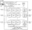
- I/O host 202 sends read and write data access requests to storage module 210 .
- the storage module includes storage controller 220 and disk drives 230 .
- Storage controller 220 performs read and write operations to satisfy the data access requests of the I/O host.
- Disk drives 230 may be connected to the storage controller via channels 0 –N.
- drives 230 may be hard disk drives. However, other storage devices, such as tape drives, optical disk drives, and the like, may be used in addition to or in place of the hardware shown in FIG. 2 .
- Storage controller 220 includes I/O cache 222 , which serves as the storage controller level 1 (L1) cache.
- I/O cache 222 may be a random access memory (RAM).
- RAM random access memory
- a typical example of a storage controller system may allocate 1 GB of memory for storage controller level 1 cache; however, more or less memory may be allocated for cache depending on the implementation.
- Solid state disk devices are essentially a non-volatile random access memory connected to an I/O channel. Due to the I/O channel protocol, memory access is not as fast for solid state disks as it is for the memory on the storage controller. However, the underlying random access memory generally has much improved I/O latency, I/O rate and sustained bandwidth as compared to hard disk drives.
- drives 230 also include solid state disk drive 232 , which serves as the storage controller level 2 cache.
- solid state disk drive 232 may be used as a second level cache by a storage processor using standard multi-level cache management algorithms.
- RAID Redundant Array of Independent Disks
- storage module 210 may include multiple solid state disk devices 232 to avoid single points of failure. With two solid state disk devices, storage controller 220 could maintain the same data in both devices. If one solid state disk failed, the other could be used to maintain data services. This configuration is referred to as RAID 1 (mirroring). With two or more solid state disk devices, other RAID organizations, such as striped parity (RAID 5), may also be used to improve the data to metadata ratio while maintaining fault tolerance.
- RAID 1 mirroring
- RAID 5 striped parity
- FIGS. 3A and 3B block diagrams are shown illustrating example storage controller architectures in accordance with a preferred embodiment of the present invention.
- FIG. 3A illustrates a single-memory storage controller architecture.
- Storage controller 300 employs a peripheral component interconnect (PCI) local bus architecture.
- PCI peripheral component interconnect
- ISA Industry Standard Architecture
- Microprocessor 302 with internal level 1 cache, and memory pool 308 are connected to PCI local bus 310 through memory controller 304 .
- Microprocessor level 2 cache 306 is also connected to memory controller 304 .
- PCI bridge 310 also may include an integrated memory controller and cache memory for processor 302 .
- ethernet adapter 314 PCI to ISA bridge 312 , drive channel adapters 316 – 318 , and host channel adapter 320 are connected to PCI bus 310 by direct component connection.
- PCI to ISA Bridge 312 provides a connection through ISA bus 330 for basic input output system (BIOS) 332 and serial port 324 .
- BIOS basic input output system
- Processor 302 is used to coordinate and provide control of various components within storage controller 300 in FIG. 3A .
- Instructions for the storage controller may be located on storage devices, such as BIOS 322 , and may be loaded into memory pool 308 for execution by processor 302 .
- Memory pool 308 is a single memory pool that is logically partitioned into two regions. A first region serves as processor memory. This portion of memory is used by processor 302 , for example, as “scratch pad” memory to perform the operations of the storage controller. The second region of memory pool 308 serves as I/O buffer memory or level 1 storage controller cache.
- Drive channel adapters 316 – 318 provide drive channels for storage devices, such as hard disk drives.
- a storage controller may have, for example, four drive channels. Each drive channel may support multiple drives per channel. The number of drives is limited by I/O hardware and communication protocol.
- solid state disks 342 , 344 are connected to at least one of the drive channel adapters, such as drive channel adapters 316 , 318 in FIG. 3A .
- Solid state disks 342 , 344 form a storage controller level 2 cache volume that is used to supplement the level 1 cache stored in memory pool 308 .
- Each solid state disk may store, for example, 8 GB of data. Therefore, read request performance may be greatly improved due to an increased probability of the data residing either in the storage controller level 1 cache or the high-speed solid state disk.
- Performance and reliability may also be improved by using RAID storage configurations.
- data may be striped (RAID 0) across solid state disks 1 –N.
- data stored on one solid state disk, such as disk 342 may be mirrored (RAID 1 ) on another solid state disk, such as disk 344 .
- RAID 1,0 or RAID 10 A combination of RAID 0 and RAID 1, referred to as RAID 1,0 or RAID 10, can also be used to stripe and mirror cache data stored on solid state disks 1 –N.
- one solid state disk may be used to store parity data (RAID 3) for the other solid state disks.
- cache data and parity data may be striped across three or more drives for performance and fault tolerance (RAID 5).
- Other RAID techniques may also be used to manage the second level cache volume stored on solid state disks 342 , 344 .
- Storage controller 350 employs a peripheral component interconnect (PCI) local bus architecture.
- PCI peripheral component interconnect
- ISA Industry Standard Architecture
- Microprocessor 352 with internal level 1 cache, and memory pool 358 are connected to PCI local bus 360 through memory controller 354 .
- Microprocessor level 2 cache 356 is also connected to memory controller 354 .
- PCI bridge 360 also may include an integrated memory controller and cache memory for processor 352 .
- Ethernet adapter 364 , PCI to ISA bridge 362 , drive channel adapters 366 – 368 , and host channel adapter 370 are connected to PCI bus 360 by direct component connection.
- PCI to ISA Bridge 362 provides a connection through ISA bus 380 for basic input output system (BIOS) 382 and serial port 384 .
- BIOS basic input output system
- Processor 352 is used to coordinate and provide control of various components within storage controller 350 in FIG. 3B . Instructions for the storage controller may be located on storage devices, such as BIOS 382 , and may be loaded into memory pool 358 for execution by processor 352 .
- Processor 352 uses memory pool 358 , for example, as a “scratch pad” memory to perform the operations of the storage controller.
- Memory pool 374 is connected to PCI bus 360 by memory controller 372 .
- Memory pool 374 serves as I/O buffer memory or level 1 storage controller cache.
- Drive channel adapters 366 – 368 provide drive channels for storage devices, such as hard disk drives.
- solid state disks 392 , 394 are connected to drive channel adapters, such as drive channel adapters 366 , 368 in FIG. 3B .
- Solid state disks 392 , 394 form a cache volume that serves as storage controller level 2 cache to supplement the level 1 cache stored in memory pool 374 .
- Each solid state disk may store, for example, 8 GB of data. Therefore, read request performance may be greatly improved due to an increased probability of the data residing either in the storage controller level 1 cache or the high-speed solid state disk. Performance and reliability may also be improved by using RAID storage configurations as discussed above with respect to FIG. 3A .
- FIGS. 3A and 3B may vary depending on the implementation and the depicted examples in FIGS. 3A and 3B and above-described examples are not meant to imply architectural limitations.
- the examples shown in FIGS. 3A and 3B illustrate bus architectures; however, the present invention may be implemented using other architectures, such as a switched architecture.
- the present invention may be implemented using a Fibre Channel architecture.
- FIG. 4A illustrates an example RAID 0 configuration.
- Cache data stream 402 is received by RAID engine 404 .
- the RAID engine manages the storage of the cache data stream onto solid state disks 406 .
- RAID engine stripes the data across the plurality of solid state disks. While this configuration may result in a slight increase in performance due to parallel reads to and/or writes to the disks, RAID 0 does not enhance reliability. Thus, the increased cost for the plurality of solid state disks will likely outweigh the performance benefit.
- RAID 1 an example RAID 1 configuration is shown in accordance with a preferred embodiment of the present invention.
- Cache data stream 412 is received by RAID engine 414 .
- the RAID engine manages the storage of the cache data stream onto solid state disks 416 .
- the RAID engine may store the cache data, for example, on a single solid state disk and mirror or copy that data onto a second solid state disk, as shown in FIG. 4B . If one of the solid state disks fails, the other disk can be used to maintain the second level storage controller cache.
- a combination of RAID 0 and RAID 1, referred to as RAID 1,0 or RAID 10 can also be used to stripe and mirror cache data stored on solid state disks 416 .
- Cache data stream 422 is received by RAID engine 424 , which manages a cache volume stored on solid state disks 426 .
- the RAID engine stripes the cache data across a plurality of the solid state disks and generates parity data from the striped cache data.
- the RAID engine stores the parity data on a separate, dedicated solid state disk drive. If a solid state disk fails, the striped data can be reconstructed using the remaining stripes and the parity data.
- RAID 3 provides the performance enhancement of RAID 0 and fault tolerance with the dedicated parity disk.
- FIG. 4D illustrates an example RAID 5 configuration in accordance with a preferred embodiment of the present invention.
- Cache data stream 432 is received by RAID engine 434 .
- the RAID engine generates parity data from the cache data and stripes the cache data and the parity data across solid state disks 436 .
- the parity data is interspersed with the striped cache data, as shown by example in FIG. 4D . If a solid state disk fails, the striped data can be reconstructed using the remaining stripes and the parity data.
- RAID 5 provides performance enhancement by reading from and writing to all of the solid state disks. Fault tolerance is provided by the parity information.
- FIGS. 4A–4D are not meant to imply architectural limitations for the present invention. For example, more or fewer solid state disks may be used depending upon the implementation.
- FIG. 5 a flowchart illustrating the operation of a storage controller is shown in accordance with a preferred embodiment of the present invention.
- the storage controller uses RAID techniques to create a cache volume.
- the storage controller then may store the cache data across the solid state disks using these RAID techniques according to the following procedure.
- the process begins and receives a data access request (step 502 ). A determination is made as to whether the data access request is a read request or a write request (step 504 ). If the data access request is a read request, a determination is made as to whether the data is in level 1 cache (step 506 ). If the data is in level 1 cache, the process fetches the data from level 1 cache (step 508 ) and the process ends. If the data is not in level 1 cache in step 506 , a determination is made as to whether the data is in the level 2 cache stored in the solid state disks (step 510 ). If the data is stored in the storage controller level 2 cache, the process fetches the data from level 2 cache volume (step 512 ) and the process ends. However, if the data is not stored in level 2 cache in step 510 , the process reads the data from the storage device (step 514 ) and ends.
- step 504 if the data access request is a write request, a determination is made as to whether the data is cached (step 516 ). If the data is cached, a determination is made as to whether the data is cached in level 1 cache or level 2 cache (step 518 ). If the data is cached in level 1 cache, the process overwrites the data in level 1 cache in memory (step 520 ) and ends. If the data is cached in level 2 cache volume in step 518 , the process overwrites the data in the level 2 cache volume (step 522 ) and the process ends.
- step 524 the process allocates space in level 1 cache for the written data (step 524 ). A determination is made as to whether level 1 cache needs to be flushed to make space to cache the written data (step 526 ). If a flush of level 1 cache is not necessary, the process ends. If, however, a flush of level 1 cache is necessary in step 526 , the process writes data from level 1 cache to the level 2 cache volume (step 528 ) and a determination is made as to whether a flush is necessary to make space to write data in level 2 cache volume (step 530 ). If a flush is not necessary, the process ends. However, if a flush is necessary in step 530 , the process flushes data from level 2 cache volume (step 532 ) and ends.
- the present invention provides a second level of storage controller cache using a solid state disk device.
- Read request performance is improved due to an increased probability of data residing in either the storage controller level 1 cache in memory or the solid state disk device.
- the present invention may also provide multiple solid state disk devices to avoid single points of failure. With two solid state disks, the storage processor could maintain the cache data in both devices. If one device fails, the other could be used to maintain data services. With two or more devices, other RAID organizations may be used to improve data-to-metadata ratio while maintaining fault tolerance. Using these RAID techniques, the plurality of solid state disks may then be organized as a single level 2 cache volume that serves as a second level cache for a storage controller.
- Retrieving the data from this second level cache is a less expensive operation than reading the data from the hard disks, especially if the data is striped across several disks as in a RAID storage system. Allowing the volumes to be configured as second level cacheable allows users to tune system performance for specific applications.
- Solid state disk devices are available in standard hard disk drive form factors. Using these devices as customer replaceable units in hard drive modules allows users to upgrade and expand simply by populating additional units in the system.
Abstract
Description
Claims (23)
Priority Applications (1)
| Application Number | Priority Date | Filing Date | Title |
|---|---|---|---|
| US10/124,647 US7149846B2 (en) | 2002-04-17 | 2002-04-17 | RAID protected external secondary memory |
Applications Claiming Priority (1)
| Application Number | Priority Date | Filing Date | Title |
|---|---|---|---|
| US10/124,647 US7149846B2 (en) | 2002-04-17 | 2002-04-17 | RAID protected external secondary memory |
Publications (2)
| Publication Number | Publication Date |
|---|---|
| US20030200388A1 US20030200388A1 (en) | 2003-10-23 |
| US7149846B2 true US7149846B2 (en) | 2006-12-12 |
Family
ID=29214627
Family Applications (1)
| Application Number | Title | Priority Date | Filing Date |
|---|---|---|---|
| US10/124,647 Expired - Fee Related US7149846B2 (en) | 2002-04-17 | 2002-04-17 | RAID protected external secondary memory |
Country Status (1)
| Country | Link |
|---|---|
| US (1) | US7149846B2 (en) |
Cited By (21)
| Publication number | Priority date | Publication date | Assignee | Title |
|---|---|---|---|---|
| US20070038830A1 (en) * | 2005-08-10 | 2007-02-15 | Koji Iwamitsu | Storage system and storage control method |
| US20100125751A1 (en) * | 2008-11-18 | 2010-05-20 | Mckean Brian | System and method for recovering solid state drive data |
| US20100162044A1 (en) * | 2004-08-09 | 2010-06-24 | Siew Yong Sim-Tang | Method for erasure coding data across a plurality of data stores in a network |
| US20100162076A1 (en) * | 2004-08-09 | 2010-06-24 | Siew Yong Sim-Tang | Method for lock-free clustered erasure coding and recovery of data across a plurality of data stores in a network |
| US20100163361A1 (en) * | 2008-12-25 | 2010-07-01 | Masayoshi Suzuta | Multiple disc clutch apparatus |
| US20100274965A1 (en) * | 2009-04-23 | 2010-10-28 | International Business Machines Corporation | Redundant solid state disk system via interconnect cards |
| US7873619B1 (en) * | 2008-03-31 | 2011-01-18 | Emc Corporation | Managing metadata |
| US20110087837A1 (en) * | 2009-10-10 | 2011-04-14 | International Business Machines Corporation | Secondary cache for write accumulation and coalescing |
| US20110099419A1 (en) * | 2009-10-23 | 2011-04-28 | International Business Machines Corporation | Solid state drive with flash sparing |
| US20110099320A1 (en) * | 2009-10-23 | 2011-04-28 | International Business Machines Corporation | Solid State Drive with Adjustable Drive Life and Capacity |
| US8805951B1 (en) | 2011-02-08 | 2014-08-12 | Emc Corporation | Virtual machines and cloud storage caching for cloud computing applications |
| US8806112B2 (en) | 2011-07-14 | 2014-08-12 | Lsi Corporation | Meta data handling within a flash media controller |
| US8812566B2 (en) | 2011-05-13 | 2014-08-19 | Nexenta Systems, Inc. | Scalable storage for virtual machines |
| US8862804B2 (en) | 2011-04-29 | 2014-10-14 | Western Digital Technologies, Inc. | System and method for improved parity determination within a data redundancy scheme in a solid state memory |
| US8954669B2 (en) | 2010-07-07 | 2015-02-10 | Nexenta System, Inc | Method and system for heterogeneous data volume |
| US8972826B2 (en) | 2012-10-24 | 2015-03-03 | Western Digital Technologies, Inc. | Adaptive error correction codes for data storage systems |
| US8984241B2 (en) | 2010-07-07 | 2015-03-17 | Nexenta Systems, Inc. | Heterogeneous redundant storage array |
| US9021339B2 (en) | 2012-11-29 | 2015-04-28 | Western Digital Technologies, Inc. | Data reliability schemes for data storage systems |
| US9059736B2 (en) | 2012-12-03 | 2015-06-16 | Western Digital Technologies, Inc. | Methods, solid state drive controllers and data storage devices having a runtime variable raid protection scheme |
| US9214963B1 (en) | 2012-12-21 | 2015-12-15 | Western Digital Technologies, Inc. | Method and system for monitoring data channel to enable use of dynamically adjustable LDPC coding parameters in a data storage system |
| US9785561B2 (en) | 2010-02-17 | 2017-10-10 | International Business Machines Corporation | Integrating a flash cache into large storage systems |
Families Citing this family (47)
| Publication number | Priority date | Publication date | Assignee | Title |
|---|---|---|---|---|
| WO2004025476A1 (en) * | 2002-09-16 | 2004-03-25 | Tigi Corporation | Storage system architectures and multiple caching arrangements |
| GB0320494D0 (en) * | 2003-09-02 | 2003-10-01 | Ibm | Methods apparatus and controllers for a raid storage system |
| WO2005041044A1 (en) * | 2003-09-24 | 2005-05-06 | Seagate Technology Llc | Multi-level caching in data storage devices |
| CA2557641A1 (en) * | 2004-02-27 | 2005-09-15 | Tigi Corporation | System and method for data manipulation |
| US7200718B2 (en) | 2004-04-26 | 2007-04-03 | Broadband Royalty Corporation | Cache memory for a scalable information distribution system |
| US7461101B2 (en) * | 2004-07-13 | 2008-12-02 | International Business Machines Corporation | Method for reducing data loss and unavailability by integrating multiple levels of a storage hierarchy |
| US7831780B2 (en) * | 2005-06-24 | 2010-11-09 | Nvidia Corporation | Operating system supplemental disk caching system and method |
| US8032650B2 (en) * | 2006-03-15 | 2011-10-04 | Arris Group, Inc. | Media stream distribution system |
| US8549236B2 (en) | 2006-12-15 | 2013-10-01 | Siliconsystems, Inc. | Storage subsystem with multiple non-volatile memory arrays to protect against data losses |
| US8930651B2 (en) | 2007-10-05 | 2015-01-06 | Imation Corp. | Archiving system with partitions of individual archives |
| US8140787B2 (en) | 2007-10-05 | 2012-03-20 | Imation Corp. | Methods for implementation of an active archive in an archiving system and managing the data in the active archive |
| US20090094423A1 (en) * | 2007-10-05 | 2009-04-09 | Prostor Systems, Inc. | Methods for implementation of an archiving system which uses removable disk storage system |
| US20100049914A1 (en) * | 2008-08-20 | 2010-02-25 | Goodwin Paul M | RAID Enhanced solid state drive |
| US8799743B2 (en) | 2008-10-28 | 2014-08-05 | Micron Technology, Inc. | Error correction in multiple semiconductor memory units |
| US8201020B2 (en) * | 2009-11-12 | 2012-06-12 | International Business Machines Corporation | Method apparatus and system for a redundant and fault tolerant solid state disk |
| US8671265B2 (en) | 2010-03-05 | 2014-03-11 | Solidfire, Inc. | Distributed data storage system providing de-duplication of data using block identifiers |
| USRE49818E1 (en) * | 2010-05-13 | 2024-01-30 | Kioxia Corporation | Information processing method in a multi-level hierarchical memory system |
| JP4988008B2 (en) * | 2010-05-13 | 2012-08-01 | 株式会社東芝 | Information processing apparatus and driver |
| JP4988007B2 (en) * | 2010-05-13 | 2012-08-01 | 株式会社東芝 | Information processing apparatus and driver |
| US8924663B2 (en) * | 2010-09-09 | 2014-12-30 | Nec Corporation | Storage system, computer-readable medium, and data management method having a duplicate storage elimination function |
| US8621157B2 (en) | 2011-06-13 | 2013-12-31 | Advanced Micro Devices, Inc. | Cache prefetching from non-uniform memories |
| US9838269B2 (en) | 2011-12-27 | 2017-12-05 | Netapp, Inc. | Proportional quality of service based on client usage and system metrics |
| US9054992B2 (en) | 2011-12-27 | 2015-06-09 | Solidfire, Inc. | Quality of service policy sets |
| WO2013145617A1 (en) * | 2012-03-29 | 2013-10-03 | パナソニック株式会社 | Information processing device, information processing method, and information storage medium |
| EP2864862B1 (en) * | 2012-07-18 | 2020-01-01 | Hitachi, Ltd. | Storage system and storage control method |
| US9542101B2 (en) * | 2013-01-22 | 2017-01-10 | Avago Technologies General Ip (Singapore) Pte. Ltd. | System and methods for performing embedded full-stripe write operations to a data volume with data elements distributed across multiple modules |
| US9110813B2 (en) * | 2013-02-14 | 2015-08-18 | Avago Technologies General Ip (Singapore) Pte Ltd | Cache load balancing in storage controllers |
| US9229870B1 (en) * | 2013-06-27 | 2016-01-05 | Emc Corporation | Managing cache systems of storage systems |
| US9251064B2 (en) * | 2014-01-08 | 2016-02-02 | Netapp, Inc. | NVRAM caching and logging in a storage system |
| US9152330B2 (en) | 2014-01-09 | 2015-10-06 | Netapp, Inc. | NVRAM data organization using self-describing entities for predictable recovery after power-loss |
| US20150244795A1 (en) | 2014-02-21 | 2015-08-27 | Solidfire, Inc. | Data syncing in a distributed system |
| US9798728B2 (en) | 2014-07-24 | 2017-10-24 | Netapp, Inc. | System performing data deduplication using a dense tree data structure |
| US9671960B2 (en) | 2014-09-12 | 2017-06-06 | Netapp, Inc. | Rate matching technique for balancing segment cleaning and I/O workload |
| US10133511B2 (en) | 2014-09-12 | 2018-11-20 | Netapp, Inc | Optimized segment cleaning technique |
| US9836229B2 (en) | 2014-11-18 | 2017-12-05 | Netapp, Inc. | N-way merge technique for updating volume metadata in a storage I/O stack |
| US9824041B2 (en) * | 2014-12-08 | 2017-11-21 | Datadirect Networks, Inc. | Dual access memory mapped data structure memory |
| US9720601B2 (en) | 2015-02-11 | 2017-08-01 | Netapp, Inc. | Load balancing technique for a storage array |
| US9762460B2 (en) | 2015-03-24 | 2017-09-12 | Netapp, Inc. | Providing continuous context for operational information of a storage system |
| US9710317B2 (en) | 2015-03-30 | 2017-07-18 | Netapp, Inc. | Methods to identify, handle and recover from suspect SSDS in a clustered flash array |
| US9740566B2 (en) | 2015-07-31 | 2017-08-22 | Netapp, Inc. | Snapshot creation workflow |
| US20170097771A1 (en) | 2015-10-01 | 2017-04-06 | Netapp, Inc. | Transaction log layout for efficient reclamation and recovery |
| US9846539B2 (en) | 2016-01-22 | 2017-12-19 | Netapp, Inc. | Recovery from low space condition of an extent store |
| US10620850B1 (en) * | 2016-03-31 | 2020-04-14 | EMC IP Holding Company LLC | Caching techniques duplicating dirty data in secondary cache |
| US10929022B2 (en) | 2016-04-25 | 2021-02-23 | Netapp. Inc. | Space savings reporting for storage system supporting snapshot and clones |
| US10642763B2 (en) | 2016-09-20 | 2020-05-05 | Netapp, Inc. | Quality of service policy sets |
| US10613764B2 (en) | 2017-11-20 | 2020-04-07 | Advanced Micro Devices, Inc. | Speculative hint-triggered activation of pages in memory |
| US11768599B2 (en) * | 2021-07-13 | 2023-09-26 | Saudi Arabian Oil Company | Managing an enterprise data storage system |
Citations (9)
| Publication number | Priority date | Publication date | Assignee | Title |
|---|---|---|---|---|
| US5734859A (en) * | 1993-10-14 | 1998-03-31 | Fujitsu Limited | Disk cache apparatus having selectable performance modes |
| US5754753A (en) * | 1992-06-11 | 1998-05-19 | Digital Equipment Corporation | Multiple-bit error correction in computer main memory |
| US5805787A (en) * | 1995-12-29 | 1998-09-08 | Emc Corporation | Disk based disk cache interfacing system and method |
| US5974503A (en) * | 1997-04-25 | 1999-10-26 | Emc Corporation | Storage and access of continuous media files indexed as lists of raid stripe sets associated with file names |
| US6321298B1 (en) * | 1999-01-25 | 2001-11-20 | International Business Machines Corporation | Full cache coherency across multiple raid controllers |
| US6330642B1 (en) * | 2000-06-29 | 2001-12-11 | Bull Hn Informatin Systems Inc. | Three interconnected raid disk controller data processing system architecture |
| US6507890B1 (en) * | 2000-09-29 | 2003-01-14 | Emc Corporation | System and method for expanding a log structure in a disk array |
| US6567889B1 (en) * | 1997-12-19 | 2003-05-20 | Lsi Logic Corporation | Apparatus and method to provide virtual solid state disk in cache memory in a storage controller |
| US6615313B2 (en) * | 2000-06-05 | 2003-09-02 | Fujitsu Limited | Disk input/output control device maintaining write data in multiple cache memory modules and method and medium thereof |
-
2002
- 2002-04-17 US US10/124,647 patent/US7149846B2/en not_active Expired - Fee Related
Patent Citations (10)
| Publication number | Priority date | Publication date | Assignee | Title |
|---|---|---|---|---|
| US5754753A (en) * | 1992-06-11 | 1998-05-19 | Digital Equipment Corporation | Multiple-bit error correction in computer main memory |
| US5734859A (en) * | 1993-10-14 | 1998-03-31 | Fujitsu Limited | Disk cache apparatus having selectable performance modes |
| US5835940A (en) * | 1993-10-14 | 1998-11-10 | Fujitsu Limited | disk apparatus with multiple raid operating modes |
| US5805787A (en) * | 1995-12-29 | 1998-09-08 | Emc Corporation | Disk based disk cache interfacing system and method |
| US5974503A (en) * | 1997-04-25 | 1999-10-26 | Emc Corporation | Storage and access of continuous media files indexed as lists of raid stripe sets associated with file names |
| US6567889B1 (en) * | 1997-12-19 | 2003-05-20 | Lsi Logic Corporation | Apparatus and method to provide virtual solid state disk in cache memory in a storage controller |
| US6321298B1 (en) * | 1999-01-25 | 2001-11-20 | International Business Machines Corporation | Full cache coherency across multiple raid controllers |
| US6615313B2 (en) * | 2000-06-05 | 2003-09-02 | Fujitsu Limited | Disk input/output control device maintaining write data in multiple cache memory modules and method and medium thereof |
| US6330642B1 (en) * | 2000-06-29 | 2001-12-11 | Bull Hn Informatin Systems Inc. | Three interconnected raid disk controller data processing system architecture |
| US6507890B1 (en) * | 2000-09-29 | 2003-01-14 | Emc Corporation | System and method for expanding a log structure in a disk array |
Non-Patent Citations (1)
| Title |
|---|
| "Memory Management for All of Us", Goodman, SAMS, 1992, pp. 513-515. |
Cited By (37)
| Publication number | Priority date | Publication date | Assignee | Title |
|---|---|---|---|---|
| US8051361B2 (en) * | 2004-08-09 | 2011-11-01 | Quest Software, Inc. | Method for lock-free clustered erasure coding and recovery of data across a plurality of data stores in a network |
| US20100162044A1 (en) * | 2004-08-09 | 2010-06-24 | Siew Yong Sim-Tang | Method for erasure coding data across a plurality of data stores in a network |
| US20100162076A1 (en) * | 2004-08-09 | 2010-06-24 | Siew Yong Sim-Tang | Method for lock-free clustered erasure coding and recovery of data across a plurality of data stores in a network |
| US8205139B1 (en) * | 2004-08-09 | 2012-06-19 | Quest Software, Inc. | Method for lock-free clustered erasure coding and recovery of data across a plurality of data stores in a network |
| US8086937B2 (en) | 2004-08-09 | 2011-12-27 | Quest Software, Inc. | Method for erasure coding data across a plurality of data stores in a network |
| US9122627B1 (en) * | 2004-08-09 | 2015-09-01 | Dell Software Inc. | Method for lock-free clustered erasure coding and recovery of data across a plurality of data stores in a network |
| US7325117B2 (en) * | 2005-08-10 | 2008-01-29 | Hitachi, Ltd. | Storage system and storage control method |
| US20070038830A1 (en) * | 2005-08-10 | 2007-02-15 | Koji Iwamitsu | Storage system and storage control method |
| US8095577B1 (en) * | 2008-03-31 | 2012-01-10 | Emc Corporation | Managing metadata |
| US7873619B1 (en) * | 2008-03-31 | 2011-01-18 | Emc Corporation | Managing metadata |
| US8041991B2 (en) * | 2008-11-18 | 2011-10-18 | Lsi Corporation | System and method for recovering solid state drive data |
| US20100125751A1 (en) * | 2008-11-18 | 2010-05-20 | Mckean Brian | System and method for recovering solid state drive data |
| US20100163361A1 (en) * | 2008-12-25 | 2010-07-01 | Masayoshi Suzuta | Multiple disc clutch apparatus |
| US8560774B2 (en) | 2009-04-23 | 2013-10-15 | International Business Machines Corporation | Redundant solid state disk system via interconnect cards |
| US20100274965A1 (en) * | 2009-04-23 | 2010-10-28 | International Business Machines Corporation | Redundant solid state disk system via interconnect cards |
| US8151051B2 (en) | 2009-04-23 | 2012-04-03 | International Business Machines Corporation | Redundant solid state disk system via interconnect cards |
| US8549225B2 (en) | 2009-10-10 | 2013-10-01 | Internatioal Business Machines Corporation | Secondary cache for write accumulation and coalescing |
| US8255627B2 (en) | 2009-10-10 | 2012-08-28 | International Business Machines Corporation | Secondary cache for write accumulation and coalescing |
| US20110087837A1 (en) * | 2009-10-10 | 2011-04-14 | International Business Machines Corporation | Secondary cache for write accumulation and coalescing |
| US8214580B2 (en) | 2009-10-23 | 2012-07-03 | International Business Machines Corporation | Solid state drive with adjustable drive life and capacity |
| US7954021B2 (en) | 2009-10-23 | 2011-05-31 | International Business Machines Corporation | Solid state drive with flash sparing |
| US20110099320A1 (en) * | 2009-10-23 | 2011-04-28 | International Business Machines Corporation | Solid State Drive with Adjustable Drive Life and Capacity |
| US20110099419A1 (en) * | 2009-10-23 | 2011-04-28 | International Business Machines Corporation | Solid state drive with flash sparing |
| US9785561B2 (en) | 2010-02-17 | 2017-10-10 | International Business Machines Corporation | Integrating a flash cache into large storage systems |
| US8984241B2 (en) | 2010-07-07 | 2015-03-17 | Nexenta Systems, Inc. | Heterogeneous redundant storage array |
| US8954669B2 (en) | 2010-07-07 | 2015-02-10 | Nexenta System, Inc | Method and system for heterogeneous data volume |
| US8990496B2 (en) | 2010-07-07 | 2015-03-24 | Nexenta Systems, Inc. | Method and system for the heterogeneous data volume |
| US9268489B2 (en) | 2010-07-07 | 2016-02-23 | Nexenta Systems, Inc. | Method and system for heterogeneous data volume |
| US8805951B1 (en) | 2011-02-08 | 2014-08-12 | Emc Corporation | Virtual machines and cloud storage caching for cloud computing applications |
| US8862804B2 (en) | 2011-04-29 | 2014-10-14 | Western Digital Technologies, Inc. | System and method for improved parity determination within a data redundancy scheme in a solid state memory |
| US8812566B2 (en) | 2011-05-13 | 2014-08-19 | Nexenta Systems, Inc. | Scalable storage for virtual machines |
| US8806112B2 (en) | 2011-07-14 | 2014-08-12 | Lsi Corporation | Meta data handling within a flash media controller |
| US8972826B2 (en) | 2012-10-24 | 2015-03-03 | Western Digital Technologies, Inc. | Adaptive error correction codes for data storage systems |
| US10216574B2 (en) | 2012-10-24 | 2019-02-26 | Western Digital Technologies, Inc. | Adaptive error correction codes for data storage systems |
| US9021339B2 (en) | 2012-11-29 | 2015-04-28 | Western Digital Technologies, Inc. | Data reliability schemes for data storage systems |
| US9059736B2 (en) | 2012-12-03 | 2015-06-16 | Western Digital Technologies, Inc. | Methods, solid state drive controllers and data storage devices having a runtime variable raid protection scheme |
| US9214963B1 (en) | 2012-12-21 | 2015-12-15 | Western Digital Technologies, Inc. | Method and system for monitoring data channel to enable use of dynamically adjustable LDPC coding parameters in a data storage system |
Also Published As
| Publication number | Publication date |
|---|---|
| US20030200388A1 (en) | 2003-10-23 |
Similar Documents
| Publication | Publication Date | Title |
|---|---|---|
| US7149846B2 (en) | RAID protected external secondary memory | |
| US7136966B2 (en) | Method and apparatus for using a solid state disk device as a storage controller cache | |
| US5586291A (en) | Disk controller with volatile and non-volatile cache memories | |
| US8938574B2 (en) | Methods and systems using solid-state drives as storage controller cache memory | |
| US7228381B2 (en) | Storage system using fast storage device for storing redundant data | |
| US6467022B1 (en) | Extending adapter memory with solid state disks in JBOD and RAID environments | |
| US7206899B2 (en) | Method, system, and program for managing data transfer and construction | |
| US8621142B1 (en) | Method and apparatus for achieving consistent read latency from an array of solid-state storage devices | |
| US9304901B2 (en) | System and method for handling I/O write requests | |
| US7730257B2 (en) | Method and computer program product to increase I/O write performance in a redundant array | |
| US6629211B2 (en) | Method and system for improving raid controller performance through adaptive write back/write through caching | |
| US8560772B1 (en) | System and method for data migration between high-performance computing architectures and data storage devices | |
| US6009481A (en) | Mass storage system using internal system-level mirroring | |
| US7213110B2 (en) | Destaging method for storage apparatus system, and disk control apparatus, storage apparatus system and program | |
| US6513102B2 (en) | Internal copy for a storage controller | |
| US8190815B2 (en) | Storage subsystem and storage system including storage subsystem | |
| US20020069317A1 (en) | E-RAID system and method of operating the same | |
| US6775738B2 (en) | Method, system, and program for caching data in a storage controller | |
| US8032610B2 (en) | Scalable high-speed cache system in a storage network | |
| US20120290786A1 (en) | Selective caching in a storage system | |
| US9098404B2 (en) | Storage array, storage system, and data access method | |
| US20100299512A1 (en) | Network Boot System | |
| US7085907B2 (en) | Dynamic reconfiguration of memory in a multi-cluster storage control unit | |
| JP2000099282A (en) | File management system | |
| US20030204677A1 (en) | Storage cache descriptor |
Legal Events
| Date | Code | Title | Description |
|---|---|---|---|
| AS | Assignment |
Owner name: LSI LOGIC CORPORATION, CALIFORNIA Free format text: ASSIGNMENT OF ASSIGNORS INTEREST;ASSIGNOR:HETRICK, WILLIAM A.;REEL/FRAME:012862/0086 Effective date: 20020415 |
|
| FEPP | Fee payment procedure |
Free format text: PAYOR NUMBER ASSIGNED (ORIGINAL EVENT CODE: ASPN); ENTITY STATUS OF PATENT OWNER: LARGE ENTITY |
|
| FPAY | Fee payment |
Year of fee payment: 4 |
|
| FPAY | Fee payment |
Year of fee payment: 8 |
|
| AS | Assignment |
Owner name: LSI CORPORATION, CALIFORNIA Free format text: CHANGE OF NAME;ASSIGNOR:LSI LOGIC CORPORATION;REEL/FRAME:033102/0270 Effective date: 20070406 |
|
| AS | Assignment |
Owner name: AVAGO TECHNOLOGIES GENERAL IP (SINGAPORE) PTE. LTD Free format text: ASSIGNMENT OF ASSIGNORS INTEREST;ASSIGNOR:LSI CORPORATION;REEL/FRAME:035390/0388 Effective date: 20140814 |
|
| AS | Assignment |
Owner name: BANK OF AMERICA, N.A., AS COLLATERAL AGENT, NORTH CAROLINA Free format text: PATENT SECURITY AGREEMENT;ASSIGNOR:AVAGO TECHNOLOGIES GENERAL IP (SINGAPORE) PTE. LTD.;REEL/FRAME:037808/0001 Effective date: 20160201 Owner name: BANK OF AMERICA, N.A., AS COLLATERAL AGENT, NORTH Free format text: PATENT SECURITY AGREEMENT;ASSIGNOR:AVAGO TECHNOLOGIES GENERAL IP (SINGAPORE) PTE. LTD.;REEL/FRAME:037808/0001 Effective date: 20160201 |
|
| AS | Assignment |
Owner name: AVAGO TECHNOLOGIES GENERAL IP (SINGAPORE) PTE. LTD., SINGAPORE Free format text: TERMINATION AND RELEASE OF SECURITY INTEREST IN PATENTS;ASSIGNOR:BANK OF AMERICA, N.A., AS COLLATERAL AGENT;REEL/FRAME:041710/0001 Effective date: 20170119 Owner name: AVAGO TECHNOLOGIES GENERAL IP (SINGAPORE) PTE. LTD Free format text: TERMINATION AND RELEASE OF SECURITY INTEREST IN PATENTS;ASSIGNOR:BANK OF AMERICA, N.A., AS COLLATERAL AGENT;REEL/FRAME:041710/0001 Effective date: 20170119 |
|
| FEPP | Fee payment procedure |
Free format text: MAINTENANCE FEE REMINDER MAILED (ORIGINAL EVENT CODE: REM.) |
|
| AS | Assignment |
Owner name: AVAGO TECHNOLOGIES INTERNATIONAL SALES PTE. LIMITE Free format text: MERGER;ASSIGNOR:AVAGO TECHNOLOGIES GENERAL IP (SINGAPORE) PTE. LTD.;REEL/FRAME:047642/0417 Effective date: 20180509 |
|
| LAPS | Lapse for failure to pay maintenance fees |
Free format text: PATENT EXPIRED FOR FAILURE TO PAY MAINTENANCE FEES (ORIGINAL EVENT CODE: EXP.); ENTITY STATUS OF PATENT OWNER: LARGE ENTITY |
|
| STCH | Information on status: patent discontinuation |
Free format text: PATENT EXPIRED DUE TO NONPAYMENT OF MAINTENANCE FEES UNDER 37 CFR 1.362 |
|
| FP | Lapsed due to failure to pay maintenance fee |
Effective date: 20181212 |
|
| AS | Assignment |
Owner name: AVAGO TECHNOLOGIES INTERNATIONAL SALES PTE. LIMITE Free format text: CORRECTIVE ASSIGNMENT TO CORRECT THE EXECUTION DATE OF THE MERGER PREVIOUSLY RECORDED ON REEL 047642 FRAME 0417. ASSIGNOR(S) HEREBY CONFIRMS THE ASSIGNMENT,;ASSIGNOR:AVAGO TECHNOLOGIES GENERAL IP (SINGAPORE) PTE. LTD.;REEL/FRAME:048521/0395 Effective date: 20180905 |