US7045472B2 - Method and apparatus for selectively altering dielectric properties of localized semiconductor device regions - Google Patents
Method and apparatus for selectively altering dielectric properties of localized semiconductor device regions Download PDFInfo
- Publication number
- US7045472B2 US7045472B2 US10/709,313 US70931304A US7045472B2 US 7045472 B2 US7045472 B2 US 7045472B2 US 70931304 A US70931304 A US 70931304A US 7045472 B2 US7045472 B2 US 7045472B2
- Authority
- US
- United States
- Prior art keywords
- dielectric
- interconnect structure
- bus bars
- interest
- semiconductor device
- Prior art date
- Legal status (The legal status is an assumption and is not a legal conclusion. Google has not performed a legal analysis and makes no representation as to the accuracy of the status listed.)
- Active, expires
Links
Images


Classifications
-
- H—ELECTRICITY
- H01—ELECTRIC ELEMENTS
- H01L—SEMICONDUCTOR DEVICES NOT COVERED BY CLASS H10
- H01L21/00—Processes or apparatus adapted for the manufacture or treatment of semiconductor or solid state devices or of parts thereof
- H01L21/70—Manufacture or treatment of devices consisting of a plurality of solid state components formed in or on a common substrate or of parts thereof; Manufacture of integrated circuit devices or of parts thereof
- H01L21/71—Manufacture of specific parts of devices defined in group H01L21/70
- H01L21/768—Applying interconnections to be used for carrying current between separate components within a device comprising conductors and dielectrics
- H01L21/76801—Applying interconnections to be used for carrying current between separate components within a device comprising conductors and dielectrics characterised by the formation and the after-treatment of the dielectrics, e.g. smoothing
- H01L21/7682—Applying interconnections to be used for carrying current between separate components within a device comprising conductors and dielectrics characterised by the formation and the after-treatment of the dielectrics, e.g. smoothing the dielectric comprising air gaps
-
- H—ELECTRICITY
- H01—ELECTRIC ELEMENTS
- H01L—SEMICONDUCTOR DEVICES NOT COVERED BY CLASS H10
- H01L21/00—Processes or apparatus adapted for the manufacture or treatment of semiconductor or solid state devices or of parts thereof
- H01L21/02—Manufacture or treatment of semiconductor devices or of parts thereof
- H01L21/02104—Forming layers
- H01L21/02107—Forming insulating materials on a substrate
- H01L21/02109—Forming insulating materials on a substrate characterised by the type of layer, e.g. type of material, porous/non-porous, pre-cursors, mixtures or laminates
- H01L21/02203—Forming insulating materials on a substrate characterised by the type of layer, e.g. type of material, porous/non-porous, pre-cursors, mixtures or laminates the layer being porous
-
- H—ELECTRICITY
- H01—ELECTRIC ELEMENTS
- H01L—SEMICONDUCTOR DEVICES NOT COVERED BY CLASS H10
- H01L21/00—Processes or apparatus adapted for the manufacture or treatment of semiconductor or solid state devices or of parts thereof
- H01L21/02—Manufacture or treatment of semiconductor devices or of parts thereof
- H01L21/02104—Forming layers
- H01L21/02107—Forming insulating materials on a substrate
- H01L21/02296—Forming insulating materials on a substrate characterised by the treatment performed before or after the formation of the layer
- H01L21/02318—Forming insulating materials on a substrate characterised by the treatment performed before or after the formation of the layer post-treatment
-
- H—ELECTRICITY
- H01—ELECTRIC ELEMENTS
- H01L—SEMICONDUCTOR DEVICES NOT COVERED BY CLASS H10
- H01L21/00—Processes or apparatus adapted for the manufacture or treatment of semiconductor or solid state devices or of parts thereof
- H01L21/02—Manufacture or treatment of semiconductor devices or of parts thereof
- H01L21/04—Manufacture or treatment of semiconductor devices or of parts thereof the devices having at least one potential-jump barrier or surface barrier, e.g. PN junction, depletion layer or carrier concentration layer
- H01L21/18—Manufacture or treatment of semiconductor devices or of parts thereof the devices having at least one potential-jump barrier or surface barrier, e.g. PN junction, depletion layer or carrier concentration layer the devices having semiconductor bodies comprising elements of Group IV of the Periodic System or AIIIBV compounds with or without impurities, e.g. doping materials
- H01L21/30—Treatment of semiconductor bodies using processes or apparatus not provided for in groups H01L21/20 - H01L21/26
- H01L21/31—Treatment of semiconductor bodies using processes or apparatus not provided for in groups H01L21/20 - H01L21/26 to form insulating layers thereon, e.g. for masking or by using photolithographic techniques; After treatment of these layers; Selection of materials for these layers
- H01L21/314—Inorganic layers
- H01L21/316—Inorganic layers composed of oxides or glassy oxides or oxide based glass
- H01L21/31695—Deposition of porous oxides or porous glassy oxides or oxide based porous glass
-
- H—ELECTRICITY
- H01—ELECTRIC ELEMENTS
- H01L—SEMICONDUCTOR DEVICES NOT COVERED BY CLASS H10
- H01L23/00—Details of semiconductor or other solid state devices
- H01L23/52—Arrangements for conducting electric current within the device in operation from one component to another, i.e. interconnections, e.g. wires, lead frames
- H01L23/522—Arrangements for conducting electric current within the device in operation from one component to another, i.e. interconnections, e.g. wires, lead frames including external interconnections consisting of a multilayer structure of conductive and insulating layers inseparably formed on the semiconductor body
- H01L23/5222—Capacitive arrangements or effects of, or between wiring layers
-
- H—ELECTRICITY
- H01—ELECTRIC ELEMENTS
- H01L—SEMICONDUCTOR DEVICES NOT COVERED BY CLASS H10
- H01L23/00—Details of semiconductor or other solid state devices
- H01L23/52—Arrangements for conducting electric current within the device in operation from one component to another, i.e. interconnections, e.g. wires, lead frames
- H01L23/522—Arrangements for conducting electric current within the device in operation from one component to another, i.e. interconnections, e.g. wires, lead frames including external interconnections consisting of a multilayer structure of conductive and insulating layers inseparably formed on the semiconductor body
- H01L23/532—Arrangements for conducting electric current within the device in operation from one component to another, i.e. interconnections, e.g. wires, lead frames including external interconnections consisting of a multilayer structure of conductive and insulating layers inseparably formed on the semiconductor body characterised by the materials
- H01L23/5329—Insulating materials
-
- H—ELECTRICITY
- H01—ELECTRIC ELEMENTS
- H01L—SEMICONDUCTOR DEVICES NOT COVERED BY CLASS H10
- H01L2224/00—Indexing scheme for arrangements for connecting or disconnecting semiconductor or solid-state bodies and methods related thereto as covered by H01L24/00
- H01L2224/01—Means for bonding being attached to, or being formed on, the surface to be connected, e.g. chip-to-package, die-attach, "first-level" interconnects; Manufacturing methods related thereto
- H01L2224/02—Bonding areas; Manufacturing methods related thereto
- H01L2224/04—Structure, shape, material or disposition of the bonding areas prior to the connecting process
- H01L2224/05—Structure, shape, material or disposition of the bonding areas prior to the connecting process of an individual bonding area
- H01L2224/05001—Internal layers
- H01L2224/05075—Plural internal layers
- H01L2224/0508—Plural internal layers being stacked
- H01L2224/05085—Plural internal layers being stacked with additional elements, e.g. vias arrays, interposed between the stacked layers
- H01L2224/05089—Disposition of the additional element
- H01L2224/05093—Disposition of the additional element of a plurality of vias
-
- H—ELECTRICITY
- H01—ELECTRIC ELEMENTS
- H01L—SEMICONDUCTOR DEVICES NOT COVERED BY CLASS H10
- H01L2924/00—Indexing scheme for arrangements or methods for connecting or disconnecting semiconductor or solid-state bodies as covered by H01L24/00
- H01L2924/01—Chemical elements
- H01L2924/01019—Potassium [K]
-
- H—ELECTRICITY
- H01—ELECTRIC ELEMENTS
- H01L—SEMICONDUCTOR DEVICES NOT COVERED BY CLASS H10
- H01L2924/00—Indexing scheme for arrangements or methods for connecting or disconnecting semiconductor or solid-state bodies as covered by H01L24/00
- H01L2924/01—Chemical elements
- H01L2924/01077—Iridium [Ir]
Definitions
- the present invention relates generally to integrated circuit devices, and, more particularly, to a method and apparatus for selectively altering dielectric properties of localized regions within an integrated circuit device.
- a first approach (which may be thought of in terms or a “hard wired” interconnection) uses the fixed layout of various conductive paths in the IC that are either diffused in the substrate or patterned in metallization layers of the IC to interconnect input and output terminals of logic gates, one to the next.
- a first approach (which may be thought of in terms or a “hard wired” interconnection) uses the fixed layout of various conductive paths in the IC that are either diffused in the substrate or patterned in metallization layers of the IC to interconnect input and output terminals of logic gates, one to the next.
- the manufacturers of integrated circuit chips have developed ways of automatically and quickly responding to orders for custom chips to perform specific functions for specific applications.
- ASIC Application Specific Integrated Circuit
- field programmable integrated circuit chips are an alternative choice.
- a field programmable chip there are several pass transistors that can be turned on or off to connect/not connect corresponding lines to logic circuits, to other lines, or to input/output pads. By turning on a particular combination of pass transistors and connecting a particular set of lines, a user can obtain a desired function. The user can also reprogram a different design into the chip by turning on different combinations of pass transistors.
- interconnection of metal lines can be achieved through a field programmable via connection typically known as an antifuse.
- the field programmable approach loses its advantage over the mask-defined approach in later phases of a product's life cycle when demand for the product grows, uncertainty about the design disappears, and chips need to be produced in relatively large volumes (e.g., 10,000 units or more).
- the total cost of the chip at such a point in its life cycle tends to be greater when the chip is a field programmable logic device (FPLD) rather than a mask-defined chip.
- FPLD field programmable logic device
- One reason field programmable chips have a larger overall cost is that the memory cells and pass transistors in field programmable chips consume large amounts of space compared to the simple metal process used in mask-defined chips.
- a circuit design may be first converted into a computer readable form using a hardware description language, or using a schematic capture program.
- Typical software design tools then perform a “logic optimization” process that includes minimizing the number of logic elements necessary to provide the logic functions defined by the circuit design.
- typical software design tools perform “technology mapping” in which logic of the circuit design is divided into component logic functions. These component logic functions are then compared to and matched with logic functions implemented by a target FPLD. Because the different FPLDs can implement different logic functions, technology mapping of a circuit design must be performed for each target FPLD. After technology mapping is complete, placement and routing are performed and a bit stream is typically generated which represents the programmed states of all of the programmable components of the target FPLD.
- a desirable alternative to conventional field programmable devices programmed through somewhat complex and time consuming software processes would be the ability to externally customize a packaged integrated circuit device by directly changing certain physical characteristics of the device, such as, for example, the dielectric constant of an insulating layer(s) therein.
- the method includes applying energy to a local region of interest, the local region of interest including a thermally alterable dielectric such that said heating caused by the applied energy causes a dielectric constant of the thermally alterable dielectric to change.
- a method for selectively altering the dielectric constant of dielectric material within a semiconductor device includes selecting the dielectric material to be a thermally alterable dielectric material within a local region of interest, and forming an interconnect structure around the local region of interest.
- the interconnect structure is further configured to provide external input/output access with respect to the semiconductor device. Energy is applied to the interconnect structure such that the heating caused by the applied energy causes the dielectric constant of the thermally alterable dielectric to change.
- an apparatus for selectively altering the dielectric constant of dielectric material within a semiconductor device includes an interconnect structure formed around a local region of interest, the interconnect structure further configured to provide external input/output access with respect to the semiconductor device.
- the dielectric material within a local region of interest is selected to be a thermally alterable dielectric material, wherein the interconnect structure is further configured such that the application of energy thereto causes the dielectric constant of the thermally alterable dielectric to change.
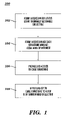
- FIG. 1 is a flow diagram illustrating a method for selectively altering the dielectric properties of a localized region(s) within an integrated circuit device, in accordance with an embodiment of the invention
- FIG. 2 is cross sectional view of a cage-shaped interconnect structure suitable for use in accordance with an embodiment of the invention
- FIG. 3 is a top view of the cage-shaped interconnect structure shown in FIG. 2 ;
- FIG. 4 is an alternative embodiment of the interconnect structure of FIGS. 2 and 3 .
- the method provides for localized heating of a dielectric that has a thermally alterable dielectric constant.
- energy e.g., electric current
- the application of energy to the interconnect structure causes localized heating of dielectric material that will (depending on the type of dielectric used) increase or decrease the dielectric constant of the material.
- the localized heating may also be carried out by other means such as, for example, application of infrared (IR) energy, laser, RF or other optical beams directed to the interconnect structure so as to heat or attenuate the surrounded dielectric.
- IR infrared
- the dielectric levels associated with a semiconductor device are formed with a dielectric material having thermally alterable dielectric constant.
- a porogen dielectric is a polymeric material that is capable of generating nanoscopic air bubbles (pores), having a dielectric constant of 1.0, within a matrix material (e.g., organosilicates) when heated so as to produce both porous inorganic and organic materials. This sacrificial porogen approach enables the production of thin-film nanoporous dielectric materials.
- the method further includes the formation of a metallic interconnect structure that surrounds certain localized areas of the porogen dielectric that may be selectively altered with respect to the dielectric constant thereof.
- the interconnect structure (described in further detail hereinafter) may be patterned and formed concurrently with the other interconnect wiring associated with the integrated circuit device. It will be noted that during the final back end of line (BEOL) manufacturing steps, the metal patterning is created such that the interconnect structure will have external I/O access thereto, as would other interconnect features of the device. This is reflected in block 106 of FIG. 1 . Finally, as shown in block 108 , energy is applied to the interconnect structure of the completed device so as to locally heat the portion of the thermally alterable dielectric surrounded by the interconnect structure.
- BEOL back end of line
- the applied energy could be in the form of electric current passed through the interconnect structure via external I/O terminals.
- the IC packaging may be made with materials transparent to optical radiation such that an applied laser, IR or UV beam, for example, acts to locally heat the dielectric.
- the applied energy could also be in the form of radio frequency (RF) or other more global energy modes. In each example, however, the dielectric is changed by application of the energy so as to alter (either lower or increase) its dielectric constant.
- RF radio frequency
- the IC device is first constructed using a suitable dielectric that either decreases or increases the K value upon the heating thereof.
- a suitable dielectric that either decreases or increases the K value upon the heating thereof.
- selectively decreasing the K value would be embodied by the use of multi-component materials wherein a porogen is activated by the applied energy thus forming small air gaps having a K value of 1.0 to lower the overall K value.
- FIG. 2 there is shown a cross sectional view of one possible implementation of a surrounding interconnect structure 200 , suitable for use in accordance with a further embodiment of the invention.
- the exemplary interconnection structure 200 is formed in a cage-like configuration, in which a plurality of metallically filled vias define a series of bars 202 that are disposed between a lower bus bar 204 and an upper bus bar 206 .
- the specific location and positioning of the bus bars 204 , 206 and bars 202 will depend upon the configuration and location of the circuit of interest that has the thermally alterable dielectric material associated therewith.
- the bars 202 may be formed by filling the vias with a metal such a tantalum (Ta) or tungsten (W) such that when electric current is passed therethrough, the bars act as filaments that will also heat the neighboring dielectric material.
- a metal such as tantalum (Ta) or tungsten (W)
- the bus bars 204 , 206 may be made from a low resistance material, such as copper, for current carrying capability.
- the use of dissimilar materials (with respect to the bus bars 204 , 206 and via filled bars 202 ) in the formation of the cage-like interconnect structure 200 might require additional masking layers, this could be prevented by using small features that (during a Ta—Cu liner/seed process) fill only with Ta, and then are so small that they do not full with adequate seed and thus become tantalum filaments.
- FIG. 3 is a top view of the cage-like interconnect structure 200 of FIG. 2 .
- the bars 202 are configured to surround a circuit of interest, denoted generally at 208 , that is surrounded with the thermally alterable dielectric material.
- the upper and lower bus bars may be formed from a unitary conductor or a series of parallel conductors, such as illustrated by upper bus bars 206 a , 206 b.
- the cage-like structure 200 represents just one possible embodiment for a surrounding interconnect structure, and that other configurations are also contemplated.
- the interconnect structure could also be configured into a solid surrounding structure 400 having walls 402 (as shown in FIG. 4 ), so long as the structure is capable of delivering heating energy to the surrounded dielectric material.
- the interconnect structure will preferably allow for passage of such gas so that the pressures created by the dielectric heating do not cause damage to the circuit interconnects or other chip area.
- gaseous byproducts e.g., CO, CO 2 , etc.
- any problem of gas evolution from porogens may be addressed by the configuration of the surrounding interconnect structure itself.
- the structure may be formed either with dedicated openings to allow the gas to relieve itself outward, such as through pipes to the outer surface of the device.
- the structure may be built to contain the pressure (and possibly even effectively become a near 100% air gap like structure, given sufficient dielectric degradation). The remaining dielectric material could then form a spider-like web of material that holds the interconnects in place, but maintains sufficient separation for operation and attains increased performance.
Abstract
Description
Claims (19)
Priority Applications (1)
| Application Number | Priority Date | Filing Date | Title |
|---|---|---|---|
| US10/709,313 US7045472B2 (en) | 2004-04-28 | 2004-04-28 | Method and apparatus for selectively altering dielectric properties of localized semiconductor device regions |
Applications Claiming Priority (1)
| Application Number | Priority Date | Filing Date | Title |
|---|---|---|---|
| US10/709,313 US7045472B2 (en) | 2004-04-28 | 2004-04-28 | Method and apparatus for selectively altering dielectric properties of localized semiconductor device regions |
Publications (2)
| Publication Number | Publication Date |
|---|---|
| US20050245098A1 US20050245098A1 (en) | 2005-11-03 |
| US7045472B2 true US7045472B2 (en) | 2006-05-16 |
Family
ID=35187683
Family Applications (1)
| Application Number | Title | Priority Date | Filing Date |
|---|---|---|---|
| US10/709,313 Active 2024-08-11 US7045472B2 (en) | 2004-04-28 | 2004-04-28 | Method and apparatus for selectively altering dielectric properties of localized semiconductor device regions |
Country Status (1)
| Country | Link |
|---|---|
| US (1) | US7045472B2 (en) |
Cited By (3)
| Publication number | Priority date | Publication date | Assignee | Title |
|---|---|---|---|---|
| US7619438B1 (en) | 2007-10-11 | 2009-11-17 | Xilinx, Inc. | Methods of enabling the use of a defective programmable device |
| US7810059B1 (en) | 2007-10-11 | 2010-10-05 | Xilinx, Inc. | Methods of enabling the validation of an integrated circuit adapted to receive one of a plurality of configuration bitstreams |
| US7853916B1 (en) | 2007-10-11 | 2010-12-14 | Xilinx, Inc. | Methods of using one of a plurality of configuration bitstreams for an integrated circuit |
Families Citing this family (6)
| Publication number | Priority date | Publication date | Assignee | Title |
|---|---|---|---|---|
| US7424655B1 (en) | 2004-10-01 | 2008-09-09 | Xilinx, Inc. | Utilizing multiple test bitstreams to avoid localized defects in partially defective programmable integrated circuits |
| US7251804B1 (en) | 2004-10-01 | 2007-07-31 | Xilinx, Inc. | Structures and methods of overcoming localized defects in programmable integrated circuits by routing during the programming thereof |
| US7284229B1 (en) | 2004-10-01 | 2007-10-16 | Xilinx, Inc. | Multiple bitstreams enabling the use of partially defective programmable integrated circuits while avoiding localized defects therein |
| US7412635B1 (en) * | 2004-10-01 | 2008-08-12 | Xilinx, Inc. | Utilizing multiple bitstreams to avoid localized defects in partially defective programmable integrated circuits |
| WO2009109932A1 (en) * | 2008-03-06 | 2009-09-11 | Nxp B.V. | Reverse engineering resistant read only memory |
| CN111886687B (en) * | 2018-01-30 | 2024-02-02 | Rnr实验室公司 | Heating device for heating target substance by laser beam and indirect heating method by laser beam |
Citations (9)
| Publication number | Priority date | Publication date | Assignee | Title |
|---|---|---|---|---|
| US5084299A (en) | 1989-08-10 | 1992-01-28 | Microelectronics And Computer Technology Corporation | Method for patterning electroless plated metal on a polymer substrate |
| US5087589A (en) | 1987-06-12 | 1992-02-11 | Massachusetts Institute Of Technology | Selectively programmable interconnections in multilayer integrated circuits |
| US5387114A (en) | 1993-07-22 | 1995-02-07 | Molex Incorporated | Electrical connector with means for altering circuit characteristics |
| US5391516A (en) | 1991-10-10 | 1995-02-21 | Martin Marietta Corp. | Method for enhancement of semiconductor device contact pads |
| US6060895A (en) | 1998-04-20 | 2000-05-09 | Fairchild Semiconductor Corp. | Wafer level dielectric test structure and related method for accelerated endurance testing |
| US6288905B1 (en) | 1999-04-15 | 2001-09-11 | Amerasia International Technology Inc. | Contact module, as for a smart card, and method for making same |
| US6519753B1 (en) | 1999-11-30 | 2003-02-11 | Quicklogic Corporation | Programmable device with an embedded portion for receiving a standard circuit design |
| US6685983B2 (en) | 2001-03-14 | 2004-02-03 | International Business Machines Corporation | Defect-free dielectric coatings and preparation thereof using polymeric nitrogenous porogens |
| US20040052948A1 (en) * | 2002-06-03 | 2004-03-18 | Shipley Company, L.L.C. | Electronic device manufacture |
-
2004
- 2004-04-28 US US10/709,313 patent/US7045472B2/en active Active
Patent Citations (9)
| Publication number | Priority date | Publication date | Assignee | Title |
|---|---|---|---|---|
| US5087589A (en) | 1987-06-12 | 1992-02-11 | Massachusetts Institute Of Technology | Selectively programmable interconnections in multilayer integrated circuits |
| US5084299A (en) | 1989-08-10 | 1992-01-28 | Microelectronics And Computer Technology Corporation | Method for patterning electroless plated metal on a polymer substrate |
| US5391516A (en) | 1991-10-10 | 1995-02-21 | Martin Marietta Corp. | Method for enhancement of semiconductor device contact pads |
| US5387114A (en) | 1993-07-22 | 1995-02-07 | Molex Incorporated | Electrical connector with means for altering circuit characteristics |
| US6060895A (en) | 1998-04-20 | 2000-05-09 | Fairchild Semiconductor Corp. | Wafer level dielectric test structure and related method for accelerated endurance testing |
| US6288905B1 (en) | 1999-04-15 | 2001-09-11 | Amerasia International Technology Inc. | Contact module, as for a smart card, and method for making same |
| US6519753B1 (en) | 1999-11-30 | 2003-02-11 | Quicklogic Corporation | Programmable device with an embedded portion for receiving a standard circuit design |
| US6685983B2 (en) | 2001-03-14 | 2004-02-03 | International Business Machines Corporation | Defect-free dielectric coatings and preparation thereof using polymeric nitrogenous porogens |
| US20040052948A1 (en) * | 2002-06-03 | 2004-03-18 | Shipley Company, L.L.C. | Electronic device manufacture |
Cited By (3)
| Publication number | Priority date | Publication date | Assignee | Title |
|---|---|---|---|---|
| US7619438B1 (en) | 2007-10-11 | 2009-11-17 | Xilinx, Inc. | Methods of enabling the use of a defective programmable device |
| US7810059B1 (en) | 2007-10-11 | 2010-10-05 | Xilinx, Inc. | Methods of enabling the validation of an integrated circuit adapted to receive one of a plurality of configuration bitstreams |
| US7853916B1 (en) | 2007-10-11 | 2010-12-14 | Xilinx, Inc. | Methods of using one of a plurality of configuration bitstreams for an integrated circuit |
Also Published As
| Publication number | Publication date |
|---|---|
| US20050245098A1 (en) | 2005-11-03 |
Similar Documents
| Publication | Publication Date | Title |
|---|---|---|
| US8945998B2 (en) | Programmable semiconductor interposer for electronic package and method of forming | |
| US7343570B2 (en) | Methods, systems, and media to improve manufacturability of semiconductor devices | |
| US7045472B2 (en) | Method and apparatus for selectively altering dielectric properties of localized semiconductor device regions | |
| US6823499B1 (en) | Method for designing application specific integrated circuit structure | |
| US6867441B1 (en) | Metal fuse structure for saving layout area | |
| US20110037497A1 (en) | Method for Fabrication of a Semiconductor Device and Structure | |
| US6214630B1 (en) | Wafer level integrated circuit structure and method of manufacturing the same | |
| US9679903B2 (en) | Anti-fuse of semiconductor device, semiconductor module and system each including the semiconductor device, and method for forming the anti-fuse | |
| US7071099B1 (en) | Forming of local and global wiring for semiconductor product | |
| US20050212011A1 (en) | Architecture for mask programmable devices | |
| Carlson et al. | Future trends in wafer scale integration | |
| JP4730192B2 (en) | Semiconductor circuit design method | |
| JP5335800B2 (en) | Semiconductor device metal programmable pooling and die | |
| US11121081B2 (en) | Antifuse element | |
| US7650584B2 (en) | Application specific semiconductor integrated circuit and its manufacturing method thereof | |
| US6784045B1 (en) | Microchannel formation for fuses, interconnects, capacitors, and inductors | |
| US20070096325A1 (en) | Semiconductor apparatus | |
| US6864171B1 (en) | Via density rules | |
| US7648912B1 (en) | ASIC customization with predefined via mask | |
| US6339559B1 (en) | Decode scheme for programming antifuses arranged in banks | |
| JP2002289817A (en) | Semiconductor integrated circuit device and its manufacturing method | |
| KR20070054278A (en) | Structure of fuse for use in semiconductor device and method for forming fuse | |
| US7241646B2 (en) | Semiconductor device having voltage output function trim circuitry and method for same | |
| JP3531863B2 (en) | Wafer-level integrated circuit structure and method for manufacturing the same | |
| US20030219946A1 (en) | Method of manufacturing semiconductor integrated circuit device |
Legal Events
| Date | Code | Title | Description |
|---|---|---|---|
| AS | Assignment |
Owner name: INTERNATIONAL BUSINESS MACHINES CORPORATION, NEW Y Free format text: ASSIGNMENT OF ASSIGNORS INTEREST;ASSIGNORS:COONEY III, EDWARD C.;MOTSIFF, WILLIAM T.;REEL/FRAME:014538/0102 Effective date: 20040409 |
|
| FEPP | Fee payment procedure |
Free format text: PAYOR NUMBER ASSIGNED (ORIGINAL EVENT CODE: ASPN); ENTITY STATUS OF PATENT OWNER: LARGE ENTITY |
|
| STCF | Information on status: patent grant |
Free format text: PATENTED CASE |
|
| FPAY | Fee payment |
Year of fee payment: 4 |
|
| REMI | Maintenance fee reminder mailed | ||
| AS | Assignment |
Owner name: TWITTER, INC., CALIFORNIA Free format text: ASSIGNMENT OF ASSIGNORS INTEREST;ASSIGNOR:INTERNATIONAL BUSINESS MACHINES CORPORATION;REEL/FRAME:032075/0404 Effective date: 20131230 |
|
| FPAY | Fee payment |
Year of fee payment: 8 |
|
| SULP | Surcharge for late payment |
Year of fee payment: 7 |
|
| FEPP | Fee payment procedure |
Free format text: MAINTENANCE FEE REMINDER MAILED (ORIGINAL EVENT CODE: REM.) |
|
| FEPP | Fee payment procedure |
Free format text: 11.5 YR SURCHARGE- LATE PMT W/IN 6 MO, LARGE ENTITY (ORIGINAL EVENT CODE: M1556) |
|
| MAFP | Maintenance fee payment |
Free format text: PAYMENT OF MAINTENANCE FEE, 12TH YEAR, LARGE ENTITY (ORIGINAL EVENT CODE: M1553) Year of fee payment: 12 |
|
| AS | Assignment |
Owner name: MORGAN STANLEY SENIOR FUNDING, INC., MARYLAND Free format text: SECURITY INTEREST;ASSIGNOR:TWITTER, INC.;REEL/FRAME:062079/0677 Effective date: 20221027 Owner name: MORGAN STANLEY SENIOR FUNDING, INC., MARYLAND Free format text: SECURITY INTEREST;ASSIGNOR:TWITTER, INC.;REEL/FRAME:061804/0086 Effective date: 20221027 Owner name: MORGAN STANLEY SENIOR FUNDING, INC., MARYLAND Free format text: SECURITY INTEREST;ASSIGNOR:TWITTER, INC.;REEL/FRAME:061804/0001 Effective date: 20221027 |
|
| AS | Assignment |
Owner name: THOMAS SCIENTIFIC, LLC, NEW JERSEY Free format text: ASSIGNMENT OF ASSIGNORS INTEREST;ASSIGNOR:NCI, INC.;REEL/FRAME:065214/0620 Effective date: 20231012 |