US7007178B2 - Voltage adaptor card for motherboard - Google Patents
Voltage adaptor card for motherboard Download PDFInfo
- Publication number
- US7007178B2 US7007178B2 US10/286,903 US28690302A US7007178B2 US 7007178 B2 US7007178 B2 US 7007178B2 US 28690302 A US28690302 A US 28690302A US 7007178 B2 US7007178 B2 US 7007178B2
- Authority
- US
- United States
- Prior art keywords
- voltage
- slots
- coupled
- adaptor card
- output terminal
- Prior art date
- Legal status (The legal status is an assumption and is not a legal conclusion. Google has not performed a legal analysis and makes no representation as to the accuracy of the status listed.)
- Expired - Lifetime, expires
Links
- 230000037431 insertion Effects 0.000 claims 1
- 238000003780 insertion Methods 0.000 claims 1
- 230000013011 mating Effects 0.000 claims 1
- 238000010586 diagram Methods 0.000 description 5
- 230000004048 modification Effects 0.000 description 3
- 238000012986 modification Methods 0.000 description 3
- 230000004075 alteration Effects 0.000 description 1
- 239000003990 capacitor Substances 0.000 description 1
- 238000004519 manufacturing process Methods 0.000 description 1
- 239000004065 semiconductor Substances 0.000 description 1
- 230000000087 stabilizing effect Effects 0.000 description 1
Images


Classifications
-
- G—PHYSICS
- G06—COMPUTING; CALCULATING OR COUNTING
- G06F—ELECTRIC DIGITAL DATA PROCESSING
- G06F1/00—Details not covered by groups G06F3/00 - G06F13/00 and G06F21/00
- G06F1/16—Constructional details or arrangements
- G06F1/18—Packaging or power distribution
- G06F1/189—Power distribution
Definitions
- the present invention relates to a voltage adaptor card for a motherboard, and particularly to a voltage adaptor card which provides required voltage through slots.
- the present invention discloses a voltage adaptor card to adapt voltage supplied from the motherboard to that suitable for interface cards.
- the voltage adaptor card in the present invention includes a voltage converter, PCI slots, and pins.
- the voltage converter includes a regulator and an adjustment circuit.
- the PCI slots provide 5V voltage.
- An output of the regulator provides interface cards inserted in the PCI slots 25 with 3.3V voltage.
- the regulator has an input terminal, an adjustment terminal, and an output terminal.
- the input terminal of the regulator is coupled to the first voltage source through the pins.
- the adjustment circuit has an input terminal and an output terminal.
- the input terminal of the adjustment circuit is coupled to the output terminal of the regulator.
- the output terminal of the adjustment circuit is coupled to the adjustment terminal of the regulator.
- the adjustment circuit is implemented by a first resistor and a second resistor.
- the first resistor is coupled between the input terminal of the adjustment circuit and the output terminal of the adjustment circuit.
- a second resistor is coupled between the output terminal of the adjustment circuit and a ground potential.
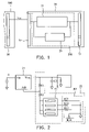
- FIG. 1 is a block diagram of the present invention.
- FIG. 2 is a block diagram of the voltage converter.
- FIG. 3 shows a table of output voltages selected by the dip switch.
- FIG. 4 shows a pin assignment of PCI slots.
- FIG. 1 is a block diagram of the present invention.
- PCI slots 10 and a voltage adaptor card 20 are shown in FIG. 1 .
- the voltage adaptor card 20 includes a voltage converter 200 , PCI slots 25 , and pins 27 .
- the voltage converter 200 includes a regulator 21 and an adjustment circuit 23 .
- the PCI slots 10 provide 5V voltage.
- An output Vout of the regulator 21 provides interface cards inserted in the PCI slots 25 with 3.3V voltage.
- FIG. 2 is a block diagram of the voltage converter.
- the voltage converter 200 includes a regulator 21 , resistors R 1 , R 2 , dip switch 32 , resistors R 11 , R 12 , R 13 , and variable resistor R 14 .
- the dip switch 32 is used for selecting resistors R 11 , R 12 , R 13 , and variable resistor R 14 .
- the regulator 21 is a linear regulator having three terminals, an input terminal Vin, an adjustment terminal Adj, and an output terminal Vout.
- the resistors R 1 , R 2 , dip switch 32 , and resistor R 3 forms an adjustment circuit 23 , a feedback circuit. A junction of the resistors R 1 and R 2 is coupled to the adjustment terminal Adj of the regulator 21 .
- the voltage of the output terminal Vout is determined by a reference voltage Vref from the regulator 21 , a ratio of the resistors R 2 and R 1 , a ratio of the resistors R 3 , selected by the dip switch 32 , and R 1 , and a product of the adjust current Iadj and resistors R 2 , R 3 .
- V out V ref(1+( R 2 + R 3 )/ R 1 )+ I adj*( R 2 + R 3 )
- a capacitor C 1 is used for frequency compensation and stabilizing the regulator 21 .
- FIG. 3 shows a table of output voltages selected by the dip switch.
- the dip switch 32 includes four switches S 1 , S 2 , S 3 , and S 4 . As shown in FIG. 3 , when the switch S 1 is turned on and the others are turned off, the dip switch 32 selects the resistor R 11 coupled to the resistor R 2 , thus the output terminal Vout of the regulator 21 has a voltage about 3V. When the switch S 2 is turned on and the others are turned off, the dip switch 32 selects the resistor R 12 coupled to the resistor R 2 , thus the output terminal Vout of the regulator 21 has a voltage about 3.3V.
- the dip switch 32 selects the resistor R 13 coupled to the resistor R 2 , thus the output terminal Vout of the regulator 21 has a voltage about 3.6V.
- the dip switch 32 selects the variable resistor R 14 coupled to the resistor R 2 thereby adjusting the output terminal Vout of the regulator 21 .
- the resistors R 11 , R 12 , and R 13 are used for coarse tuning, and the variable resistor R 14 for fine tuning.
- FIG. 4 is a block diagram of PCI slots. As shown in FIG. 4 , both the PCI slots 10 and the PCI slots 25 have pins A 11 , A 15 , A 17 , A 19 , a 21 , A 23 , and A 25 , assigned for 5V by the outdated PCI spec, and unused pins B 11 , B 15 , B 17 , B 19 , B 21 , B 23 , B 25 , and B 29 . The unused pins B 11 , B 15 , B 17 , B 19 , B 21 , B 23 , B 25 , and B 29 are assigned for 3.3V by new PCI spec.
- the PCI slots 10 are located in the motherboard 300 , providing only 5V voltage.
- the voltage adaptor card has the following advantages.
Abstract
A voltage adaptor card. The voltage adaptor card, inserted into a motherboard having first slots to provide a first voltage source, includes second slots, a plurality of pins for inserting into the first slots, and a voltage converter having an input terminal and an output terminal. The input terminal is coupled to the first voltage source through the plurality of pins. The output terminal is coupled to the second slots and outputs a second voltage source.
Description
1. Field of the Invention
The present invention relates to a voltage adaptor card for a motherboard, and particularly to a voltage adaptor card which provides required voltage through slots.
2. Description of the Related Art
Owing to low power requirement and progress in semiconductor fabrication, operating voltages of most integrated circuits are reduced, as are most PCI interface cards. Because PCI slots on motherboards compliant with only the outdated PCI spec only provide 5V voltage without 3.3V voltage, either the motherboard compliant with only the outdated PCI spec or the PCI card itself must be modified to provide both 5V and 3.3V voltages.
To avoid modification of motherboards compliant with only the outdated PCI spec or PCI interface card, there is a need for a voltage adaptor card which provides required voltages.
It is therefore an object of the present invention to provide a motherboard with a single voltage source, providing various voltage sources required by interface cards.
To achieve the above objects, the present invention discloses a voltage adaptor card to adapt voltage supplied from the motherboard to that suitable for interface cards.
The voltage adaptor card in the present invention includes a voltage converter, PCI slots, and pins. The voltage converter includes a regulator and an adjustment circuit. The PCI slots provide 5V voltage. An output of the regulator provides interface cards inserted in the PCI slots 25 with 3.3V voltage.
The regulator has an input terminal, an adjustment terminal, and an output terminal. The input terminal of the regulator is coupled to the first voltage source through the pins.
The adjustment circuit has an input terminal and an output terminal. The input terminal of the adjustment circuit is coupled to the output terminal of the regulator. The output terminal of the adjustment circuit is coupled to the adjustment terminal of the regulator.
The adjustment circuit is implemented by a first resistor and a second resistor. The first resistor is coupled between the input terminal of the adjustment circuit and the output terminal of the adjustment circuit. A second resistor is coupled between the output terminal of the adjustment circuit and a ground potential.
The aforementioned objects, features and advantages of this invention will become apparent by referring to the following detailed description of the preferred embodiment with reference to the accompanying drawings, wherein:
Vout=Vref(1+(R 2+R 3)/R 1)+Iadj*(R 2+R 3)
A capacitor C1 is used for frequency compensation and stabilizing the
The voltage adaptor card has the following advantages.
-
- (1) The voltage converter adapts voltage to that required for PCI slots from the motherboard, for broader application.
- (2) The voltage of the PCI slots is adjusted by feedback resistors thereby testing interface cards on the PCI slots. The motherboards providing single voltage can continue to be used without modification.
Although the present invention has been described in its preferred embodiments, it is not intended to limit the invention to the precise embodiments disclosed herein. Those who are skilled in this technology can still make various alterations and modifications without departing from the scope and spirit of this invention. Therefore, the scope of the present invention shall be defined and protected by the following claims and their equivalents.
Claims (17)
1. A voltage adaptor card for a motherboard having first slots to provide a first voltage source, comprising:
second slots;
a plurality of pins for insertion into the first slots; and
a voltage converter having an input terminal and an output terminal, wherein the input terminal is coupled to the first voltage source through the plurality of pins, and the output terminal is coupled to the second slots and outputs a second voltage source;
a regulator having a first input terminal, an adjustment terminal, and a first output terminal, wherein the input terminal of the regulator is coupled to the first voltage source through the plurality of pins; and
an adjustment circuit having a second input terminal and a second output terminal, wherein the input terminal of the adjustment circuit is coupled to the output terminal of the regulator, and the output terminal of the adjustment circuit is coupled to the adjustment terminal of the regulator.
2. The voltage adaptor card as claimed in claim 1 wherein the adjustment circuit includes:
a first resistor coupled between the second input terminal of the adjustment circuit and the second output terminal of the adjustment circuit; and
a second resistor coupled between the second output terminal of the adjustment circuit and a ground potential.
3. The voltage adaptor card as claimed in claim 1 wherein the adjustment circuit includes:
a first resistor coupled between the second input terminal of the adjustment circuit and the second output terminal of the adjustment circuit;
a second resistor coupled to the second output terminal of the adjustment circuit;
a dip switch having a plurality of first terminals, a plurality of second terminals, and a plurality of switches, wherein the plurality of first terminals are all coupled to the second resistor, the plurality of switches are used for selecting the plurality of first terminals coupled to the plurality of second terminals; and
a plurality of third resistors coupled between the plurality of second terminals of the dip switch and a ground potential.
4. The voltage adaptor card as claimed in claim 3 wherein the plurality of third resistors includes a variable resistor.
5. The voltage adaptor card as claimed in claim 1 wherein the first slots are PCI slots.
6. The voltage adaptor card as claimed in claim 1 wherein the second slots are PCI slots.
7. The voltage adaptor card as claimed in claim 1 wherein the first voltage source has a voltage of 5V.
8. The voltage adaptor card as claimed in claim 1 wherein the second voltage source has a voltage of 3.3V.
9. A voltage adaptor card for a motherboard having first slots to provide the first voltage source, comprising:
second slots;
a plurality of pins for inserting the first slots;
a regulator having an input terminal, an adjustment terminal, and an output terminal, wherein the input terminal of the regulator is coupled to the first voltage source through the plurality of pins, and the output terminal is coupled to the second slots and outputs a second voltage source;
a first resistor coupled between the output terminal of the regulator and the adjustment terminal of the regulator; and
a second resistor coupled between the adjustment terminal of the regulator and a ground potential.
10. The voltage adaptor card as claimed in claim 9 further comprising:
a dip switch having a plurality of first terminals, a plurality of second terminals, and a plurality of switches, wherein the plurality of first terminals are all coupled to the second resistor, and the plurality of switches are used for selecting the plurality of first terminals coupled to the plurality of second terminals; and
a plurality of third resistors coupled between the plurality of second terminals of the dip switch and the ground potential.
11. The voltage adaptor card as claimed in claim 10 wherein the plurality of third resistors includes a variable resistor.
12. The voltage adaptor card as claimed in claim 9 wherein the first slots are PCI slots.
13. The voltage adaptor card as claimed in claim 9 wherein the second slots are PCI slots.
14. The voltage adaptor card as claimed in claim 9 wherein the first voltage source has a voltage of 5V.
15. The voltage adaptor card as claimed in claim 1 wherein the second voltage source has a voltage of 3.3V.
16. The voltage adaptor card as claimed in claim 1 wherein the first slots are PCI slots and the second slots are PCI slots.
17. The voltage adaptor card as claimed in claim 1 wherein the second slots are similar in configuration to the first slots, whereby plurality of the voltage card are mutually interconnectable by mating the second slots of a first one of the voltage card with the pins of a second one the voltage cards.
Applications Claiming Priority (2)
| Application Number | Priority Date | Filing Date | Title |
|---|---|---|---|
| TW91211313 | 2002-07-24 | ||
| TW91211313U TW564969U (en) | 2002-07-24 | 2002-07-24 | Voltage conversion card on a motherboard |
Publications (2)
| Publication Number | Publication Date |
|---|---|
| US20040017114A1 US20040017114A1 (en) | 2004-01-29 |
| US7007178B2 true US7007178B2 (en) | 2006-02-28 |
Family
ID=30768982
Family Applications (1)
| Application Number | Title | Priority Date | Filing Date |
|---|---|---|---|
| US10/286,903 Expired - Lifetime US7007178B2 (en) | 2002-07-24 | 2002-11-04 | Voltage adaptor card for motherboard |
Country Status (2)
| Country | Link |
|---|---|
| US (1) | US7007178B2 (en) |
| TW (1) | TW564969U (en) |
Cited By (3)
| Publication number | Priority date | Publication date | Assignee | Title |
|---|---|---|---|---|
| US7301847B2 (en) | 2004-03-12 | 2007-11-27 | Wistron Corp. | Method and device for a main board commonly associated with DDR2 or DDR1 |
| US20110047391A1 (en) * | 2009-08-20 | 2011-02-24 | Hon Hai Precision Industry Co., Ltd. | Electronic device and motherboard thereof |
| CN102934041A (en) * | 2010-06-09 | 2013-02-13 | 亚马逊科技公司 | Power routing device for expansion slot of computer system |
Families Citing this family (4)
| Publication number | Priority date | Publication date | Assignee | Title |
|---|---|---|---|---|
| US20090240863A1 (en) * | 2007-10-23 | 2009-09-24 | Psion Teklogix Inc. | Distributed power regulation |
| CN101634962B (en) * | 2008-07-21 | 2011-11-09 | 鸿富锦精密工业(深圳)有限公司 | PCI interface test card |
| CN102955496A (en) * | 2011-08-18 | 2013-03-06 | 鸿富锦精密工业(深圳)有限公司 | Load board |
| US10398032B1 (en) | 2018-03-23 | 2019-08-27 | Amazon Technologies, Inc. | Modular expansion card bus |
Citations (10)
| Publication number | Priority date | Publication date | Assignee | Title |
|---|---|---|---|---|
| US5497037A (en) * | 1994-07-14 | 1996-03-05 | Advanced Micro Devices, Inc. | Method and apparatus for decoupling of unused power supply pins of a printed circuit board capable of operating at a plurality of predetermined voltages |
| US5758100A (en) * | 1996-07-01 | 1998-05-26 | Sun Microsystems, Inc. | Dual voltage module interconnect |
| US5911050A (en) * | 1997-07-01 | 1999-06-08 | International Business Machines Corporation | System for connecting either of two supply voltage type PCI cards using a common connector socket |
| US6031297A (en) * | 1998-01-22 | 2000-02-29 | International Business Machines Corporation | Printed circuit board allowing usage of alternative pin-compatible modules |
| US6091617A (en) * | 1999-01-21 | 2000-07-18 | Dell Usa, Lp | Automatic power supply selector for ACPI-compliant PCI devices |
| US6256692B1 (en) * | 1997-10-13 | 2001-07-03 | Fujitsu Limited | CardBus interface circuit, and a CardBus PC having the same |
| US6264506B1 (en) * | 1999-04-23 | 2001-07-24 | J.S.T. Mfg. Co., Ltd. | Card connection adapter |
| US6269416B1 (en) * | 1999-02-02 | 2001-07-31 | Hewlett-Packard Company | Adaptive PCI slot |
| US6554195B1 (en) * | 1999-06-24 | 2003-04-29 | Via Technologies, Inc. | Dual processor adapter card |
| US6701400B2 (en) * | 1999-03-24 | 2004-03-02 | Dell Products L.P. | Adaptive card-sensitive bus slot method and system |
-
2002
- 2002-07-24 TW TW91211313U patent/TW564969U/en not_active IP Right Cessation
- 2002-11-04 US US10/286,903 patent/US7007178B2/en not_active Expired - Lifetime
Patent Citations (11)
| Publication number | Priority date | Publication date | Assignee | Title |
|---|---|---|---|---|
| US5497037A (en) * | 1994-07-14 | 1996-03-05 | Advanced Micro Devices, Inc. | Method and apparatus for decoupling of unused power supply pins of a printed circuit board capable of operating at a plurality of predetermined voltages |
| US5758100A (en) * | 1996-07-01 | 1998-05-26 | Sun Microsystems, Inc. | Dual voltage module interconnect |
| US5911050A (en) * | 1997-07-01 | 1999-06-08 | International Business Machines Corporation | System for connecting either of two supply voltage type PCI cards using a common connector socket |
| US6256692B1 (en) * | 1997-10-13 | 2001-07-03 | Fujitsu Limited | CardBus interface circuit, and a CardBus PC having the same |
| US6031297A (en) * | 1998-01-22 | 2000-02-29 | International Business Machines Corporation | Printed circuit board allowing usage of alternative pin-compatible modules |
| US6091617A (en) * | 1999-01-21 | 2000-07-18 | Dell Usa, Lp | Automatic power supply selector for ACPI-compliant PCI devices |
| US6841898B2 (en) * | 1999-01-21 | 2005-01-11 | Dell Usa, L.P. | Automatic power supply selector for a ACPI-compliant PCI devices |
| US6269416B1 (en) * | 1999-02-02 | 2001-07-31 | Hewlett-Packard Company | Adaptive PCI slot |
| US6701400B2 (en) * | 1999-03-24 | 2004-03-02 | Dell Products L.P. | Adaptive card-sensitive bus slot method and system |
| US6264506B1 (en) * | 1999-04-23 | 2001-07-24 | J.S.T. Mfg. Co., Ltd. | Card connection adapter |
| US6554195B1 (en) * | 1999-06-24 | 2003-04-29 | Via Technologies, Inc. | Dual processor adapter card |
Cited By (4)
| Publication number | Priority date | Publication date | Assignee | Title |
|---|---|---|---|---|
| US7301847B2 (en) | 2004-03-12 | 2007-11-27 | Wistron Corp. | Method and device for a main board commonly associated with DDR2 or DDR1 |
| US20110047391A1 (en) * | 2009-08-20 | 2011-02-24 | Hon Hai Precision Industry Co., Ltd. | Electronic device and motherboard thereof |
| CN102934041A (en) * | 2010-06-09 | 2013-02-13 | 亚马逊科技公司 | Power routing device for expansion slot of computer system |
| CN102934041B (en) * | 2010-06-09 | 2016-08-24 | 亚马逊科技公司 | The power-supply wiring equipment of expansion slot in computer system |
Also Published As
| Publication number | Publication date |
|---|---|
| US20040017114A1 (en) | 2004-01-29 |
| TW564969U (en) | 2003-12-01 |
Similar Documents
| Publication | Publication Date | Title |
|---|---|---|
| US7859325B2 (en) | CPU core voltage supply circuit | |
| US7358708B2 (en) | Linear voltage regulator | |
| US7893671B2 (en) | Regulator with improved load regulation | |
| US20190050013A1 (en) | Method for Adaptive Compensation of Linear Voltage Regulators | |
| US20020075710A1 (en) | Power converter with adjustable output voltage | |
| US20120293244A1 (en) | Charge pump circuits and methods | |
| US7701183B2 (en) | Power circuit and charge pumping circuit | |
| US7489185B2 (en) | Voltage converting circuit structure | |
| US8159797B2 (en) | Overvoltage protection circuit | |
| CA2299525A1 (en) | A buck boost switching regulator | |
| US7007178B2 (en) | Voltage adaptor card for motherboard | |
| US20080315849A1 (en) | Power Converter and Method for Power Conversion | |
| CN111742477A (en) | Multiple input voltage regulator | |
| CN112363558A (en) | Voltage regulating circuit | |
| US6600297B2 (en) | Power supply unit for regulating output voltage using a series regulator | |
| US5726875A (en) | AC-DC adapter | |
| US11237586B2 (en) | Reference voltage generating circuit | |
| JP2003180073A (en) | Power supply circuit | |
| US6975163B2 (en) | Precision margining circuitry | |
| CN111831046A (en) | Output stage circuit and voltage stabilizer thereof | |
| JP2007219901A (en) | Reference current source circuit | |
| CN1226680C (en) | Voltage converting card suitable for mainboard | |
| US20060108990A1 (en) | Linearly regulated power supply | |
| EP2075668A2 (en) | CPU core voltage supply circuit | |
| JPH11353041A (en) | Dc power unit |
Legal Events
| Date | Code | Title | Description |
|---|---|---|---|
| AS | Assignment |
Owner name: VIA TECHNOLOGIES, INC., TAIWAN Free format text: ASSIGNMENT OF ASSIGNORS INTEREST;ASSIGNORS:TSENG, YI-KANG;CHANG, WEN-CHING;REEL/FRAME:013464/0221 Effective date: 20021008 |
|
| STCF | Information on status: patent grant |
Free format text: PATENTED CASE |
|
| FPAY | Fee payment |
Year of fee payment: 4 |
|
| FPAY | Fee payment |
Year of fee payment: 8 |
|
| FPAY | Fee payment |
Year of fee payment: 12 |