US6995897B2 - Deformable mirror and information device having the deformable mirror - Google Patents
Deformable mirror and information device having the deformable mirror Download PDFInfo
- Publication number
- US6995897B2 US6995897B2 US11/088,207 US8820705A US6995897B2 US 6995897 B2 US6995897 B2 US 6995897B2 US 8820705 A US8820705 A US 8820705A US 6995897 B2 US6995897 B2 US 6995897B2
- Authority
- US
- United States
- Prior art keywords
- light
- wave front
- medium
- optical
- information device
- Prior art date
- Legal status (The legal status is an assumption and is not a legal conclusion. Google has not performed a legal analysis and makes no representation as to the accuracy of the status listed.)
- Expired - Lifetime
Links
Images


Classifications
-
- G—PHYSICS
- G11—INFORMATION STORAGE
- G11B—INFORMATION STORAGE BASED ON RELATIVE MOVEMENT BETWEEN RECORD CARRIER AND TRANSDUCER
- G11B7/00—Recording or reproducing by optical means, e.g. recording using a thermal beam of optical radiation by modifying optical properties or the physical structure, reproducing using an optical beam at lower power by sensing optical properties; Record carriers therefor
- G11B7/12—Heads, e.g. forming of the optical beam spot or modulation of the optical beam
- G11B7/135—Means for guiding the beam from the source to the record carrier or from the record carrier to the detector
- G11B7/1362—Mirrors
-
- G—PHYSICS
- G02—OPTICS
- G02B—OPTICAL ELEMENTS, SYSTEMS OR APPARATUS
- G02B3/00—Simple or compound lenses
- G02B3/0006—Arrays
- G02B3/0037—Arrays characterized by the distribution or form of lenses
- G02B3/0062—Stacked lens arrays, i.e. refractive surfaces arranged in at least two planes, without structurally separate optical elements in-between
- G02B3/0068—Stacked lens arrays, i.e. refractive surfaces arranged in at least two planes, without structurally separate optical elements in-between arranged in a single integral body or plate, e.g. laminates or hybrid structures with other optical elements
-
- G—PHYSICS
- G02—OPTICS
- G02B—OPTICAL ELEMENTS, SYSTEMS OR APPARATUS
- G02B26/00—Optical devices or arrangements for the control of light using movable or deformable optical elements
- G02B26/06—Optical devices or arrangements for the control of light using movable or deformable optical elements for controlling the phase of light
-
- G—PHYSICS
- G02—OPTICS
- G02B—OPTICAL ELEMENTS, SYSTEMS OR APPARATUS
- G02B26/00—Optical devices or arrangements for the control of light using movable or deformable optical elements
- G02B26/08—Optical devices or arrangements for the control of light using movable or deformable optical elements for controlling the direction of light
- G02B26/0816—Optical devices or arrangements for the control of light using movable or deformable optical elements for controlling the direction of light by means of one or more reflecting elements
- G02B26/0825—Optical devices or arrangements for the control of light using movable or deformable optical elements for controlling the direction of light by means of one or more reflecting elements the reflecting element being a flexible sheet or membrane, e.g. for varying the focus
-
- G—PHYSICS
- G02—OPTICS
- G02B—OPTICAL ELEMENTS, SYSTEMS OR APPARATUS
- G02B26/00—Optical devices or arrangements for the control of light using movable or deformable optical elements
- G02B26/08—Optical devices or arrangements for the control of light using movable or deformable optical elements for controlling the direction of light
- G02B26/0816—Optical devices or arrangements for the control of light using movable or deformable optical elements for controlling the direction of light by means of one or more reflecting elements
- G02B26/0833—Optical devices or arrangements for the control of light using movable or deformable optical elements for controlling the direction of light by means of one or more reflecting elements the reflecting element being a micromechanical device, e.g. a MEMS mirror, DMD
- G02B26/0841—Optical devices or arrangements for the control of light using movable or deformable optical elements for controlling the direction of light by means of one or more reflecting elements the reflecting element being a micromechanical device, e.g. a MEMS mirror, DMD the reflecting element being moved or deformed by electrostatic means
-
- G—PHYSICS
- G02—OPTICS
- G02B—OPTICAL ELEMENTS, SYSTEMS OR APPARATUS
- G02B3/00—Simple or compound lenses
- G02B3/0006—Arrays
- G02B3/0037—Arrays characterized by the distribution or form of lenses
- G02B3/0043—Inhomogeneous or irregular arrays, e.g. varying shape, size, height
-
- G—PHYSICS
- G02—OPTICS
- G02B—OPTICAL ELEMENTS, SYSTEMS OR APPARATUS
- G02B3/00—Simple or compound lenses
- G02B3/0006—Arrays
- G02B3/0037—Arrays characterized by the distribution or form of lenses
- G02B3/005—Arrays characterized by the distribution or form of lenses arranged along a single direction only, e.g. lenticular sheets
-
- G—PHYSICS
- G02—OPTICS
- G02B—OPTICAL ELEMENTS, SYSTEMS OR APPARATUS
- G02B3/00—Simple or compound lenses
- G02B3/0006—Arrays
- G02B3/0037—Arrays characterized by the distribution or form of lenses
- G02B3/0056—Arrays characterized by the distribution or form of lenses arranged along two different directions in a plane, e.g. honeycomb arrangement of lenses
-
- G—PHYSICS
- G11—INFORMATION STORAGE
- G11B—INFORMATION STORAGE BASED ON RELATIVE MOVEMENT BETWEEN RECORD CARRIER AND TRANSDUCER
- G11B7/00—Recording or reproducing by optical means, e.g. recording using a thermal beam of optical radiation by modifying optical properties or the physical structure, reproducing using an optical beam at lower power by sensing optical properties; Record carriers therefor
- G11B7/12—Heads, e.g. forming of the optical beam spot or modulation of the optical beam
- G11B7/123—Integrated head arrangements, e.g. with source and detectors mounted on the same substrate
- G11B7/124—Integrated head arrangements, e.g. with source and detectors mounted on the same substrate the integrated head arrangements including waveguides
-
- G—PHYSICS
- G11—INFORMATION STORAGE
- G11B—INFORMATION STORAGE BASED ON RELATIVE MOVEMENT BETWEEN RECORD CARRIER AND TRANSDUCER
- G11B7/00—Recording or reproducing by optical means, e.g. recording using a thermal beam of optical radiation by modifying optical properties or the physical structure, reproducing using an optical beam at lower power by sensing optical properties; Record carriers therefor
- G11B7/12—Heads, e.g. forming of the optical beam spot or modulation of the optical beam
- G11B7/13—Optical detectors therefor
- G11B7/131—Arrangement of detectors in a multiple array
-
- G—PHYSICS
- G11—INFORMATION STORAGE
- G11B—INFORMATION STORAGE BASED ON RELATIVE MOVEMENT BETWEEN RECORD CARRIER AND TRANSDUCER
- G11B7/00—Recording or reproducing by optical means, e.g. recording using a thermal beam of optical radiation by modifying optical properties or the physical structure, reproducing using an optical beam at lower power by sensing optical properties; Record carriers therefor
- G11B7/12—Heads, e.g. forming of the optical beam spot or modulation of the optical beam
- G11B7/135—Means for guiding the beam from the source to the record carrier or from the record carrier to the detector
- G11B7/1365—Separate or integrated refractive elements, e.g. wave plates
- G11B7/1369—Active plates, e.g. liquid crystal panels or electrostrictive elements
-
- G—PHYSICS
- G11—INFORMATION STORAGE
- G11B—INFORMATION STORAGE BASED ON RELATIVE MOVEMENT BETWEEN RECORD CARRIER AND TRANSDUCER
- G11B7/00—Recording or reproducing by optical means, e.g. recording using a thermal beam of optical radiation by modifying optical properties or the physical structure, reproducing using an optical beam at lower power by sensing optical properties; Record carriers therefor
- G11B7/12—Heads, e.g. forming of the optical beam spot or modulation of the optical beam
- G11B7/135—Means for guiding the beam from the source to the record carrier or from the record carrier to the detector
- G11B7/1392—Means for controlling the beam wavefront, e.g. for correction of aberration
- G11B7/13925—Means for controlling the beam wavefront, e.g. for correction of aberration active, e.g. controlled by electrical or mechanical means
- G11B7/13927—Means for controlling the beam wavefront, e.g. for correction of aberration active, e.g. controlled by electrical or mechanical means during transducing, e.g. to correct for variation of the spherical aberration due to disc tilt or irregularities in the cover layer thickness
-
- G—PHYSICS
- G11—INFORMATION STORAGE
- G11B—INFORMATION STORAGE BASED ON RELATIVE MOVEMENT BETWEEN RECORD CARRIER AND TRANSDUCER
- G11B7/00—Recording or reproducing by optical means, e.g. recording using a thermal beam of optical radiation by modifying optical properties or the physical structure, reproducing using an optical beam at lower power by sensing optical properties; Record carriers therefor
- G11B2007/0003—Recording, reproducing or erasing systems characterised by the structure or type of the carrier
- G11B2007/0006—Recording, reproducing or erasing systems characterised by the structure or type of the carrier adapted for scanning different types of carrier, e.g. CD & DVD
Definitions
- the present invention relates to a deformable mirror comprising a displaceable light reflecting area, and an information device capable of reading information out of a storage medium and/or writing information onto a storage medium.
- the invention also relates to an optical compensation device and a wave front detection device for detecting and correcting the wave front of light beams coming incident from an external light source or of light beams from a light source provided inside.
- the optical disk device irradiates an optical disk, which is its recording medium, with forward light emitted from a laser beam source and detects variations in the intensity of the reflected backward light. Then, information recorded on the optical disk can be detected on the basis of these variations in the backward light.
- This kind of information device requires keeping the spot shape of the light beams appropriate to ensure highly reliable reproduction or recording. For this purpose, it is essential to suppress wave front aberrations of the light beams arising on the optical path.
- wave front aberrations may arise from any of a wide variety of causes including a tilt of the optical axis of the light beams relative to the recording layer of the disk, a variation in the thickness of the disk substrate and the smear of the disk surface with a fingerprint or the like, and the type of wave front aberration may vary with the cause. For instance, wave front aberrations due to tilts are predominantly coma aberrations and astigmatisms, while wave front aberration due to a variation in the thickness of the disk substrate are predominantly spherical aberrations.
- a light source 101 such as a semiconductor laser
- a wave front converting element 304 After passing a half mirror 302 and being converted into substantially parallel light by a collimating lens 303 .
- the transmitted light is subsequently brought to incidence by an objective lens 305 onto the write/read information layer through the substrate of an optical disk 306 .
- the light beams reflected by the write/read information layer of the optical disk 306 are again transmitted by the substrate, and transmitted successively by the objective lens 305 , the wave front converting element 304 and the collimating lens 303 . After they are reflected by the half mirror 302 , they are diffracted by a hologram 309 and brought to incidence on an optical detector 307 for signal detection use.
- the optical detector 307 is configured of optical detecting elements, such as pin diodes, for detecting information signals, control signals including focusing signals and tracking signals, and aberrations of light beams. These detecting elements may either be individually configured for different modes of signal detection or perform a plurality of functions by integrating them.
- the detected aberrations are processed by a signal processing circuit 308 and drive the wave front converting element 304 .
- the wave front converting element 304 is an element comprising two glass substrates between which liquid crystals are sealed in.
- the part which light beams pass are divided into a plurality of areas, and a voltage is applied to each area independently of others to vary the refractive index of the corresponding part and thereby to change the phase of the wave front.
- FIG. 26( b ) A configuration for detecting coma aberrations in particular, out of different wave front aberrations, is shown in FIG. 26( b ) to exemplify the optical detector 307 and the hologram 309 .
- the configuration is such that the light spot 314 be formed to focus on the line dividing the optical detectors 317 a and 317 b from each other when there is no aberration.
- the area 313 is so set that, when any coma aberration has arisen in the direction of the Y axis, light beams ahead of or behind the light beams passing other areas than this in phase can be extracted
- the quantity and sign of the coma aberration are determined.
- FIG. 26( c ) a configuration for detecting spherical aberrations in particular is shown in FIG. 26( c ).
- An optical axis 310 is supposed to pass the origin of the X-Y coordinate system. In light beams 322 on the backward path, on which the beams reflected by the optical disk are condensed, only those passing the area 323 of Y>0, out of the areas between two concentric circles of differing diameters around the optical axis 310 are separated from the light beams passing other areas than the area 323 , and condensed into bisected optical detectors 317 a and 317 b to cause a light spot 324 to be formed.
- the configuration is such that the light spot 324 be formed to focus on the line dividing the optical detectors 317 a and 317 b from each other when there is no aberration.
- the area 323 is so set that, when any spherical aberration has arisen, light beams ahead of or behind the light beams passing other areas than this in phase can be extracted.
- the quantity and sign of the spherical aberration are determined.
- Other aberrations for instance astigmatisms, can be detected if the arrangement and shapes of the optical detector 307 and the hologram 309 are optimally designed.
- the wave front converting element 304 a deformable mirror system by which the optical path length is controlled by deforming a flexible deformable mirror, and this technique is disclosed in the Japanese Patent Laid-Open No. 11-14918.
- the configuration here is such that a metallic thin film is vapor-deposited on the surface of a flexible deformable plate to make it a mirror surface, an electrode is provided on the rear side of the deformable plate in the opposite position with a prescribed gap in-between, and the deformable plate is attracted with an electrostatic force by applying a voltage to this electrode.
- the only driving force in the reverse direction is only a passive one deriving from the righting force of the deformable plate which has been once deformed, and this lack of symmetry of the driving forces results in poor control accuracy and responsiveness.
- bidirectional driving by utilizing such a passive force inevitably requires the use of a position deformed in advance to some extent as the reference face, it is made difficult to reproduce the shape of the reference face stably by fluctuations in drive sensitivity from one unit to another, and this invites a deterioration in the accuracy of correction.
- the main object of the present invention is to provide a deformable mirror adaptable to a broad variety of aberration types and capable of correcting wave front aberrations, which is accurate, broad in correctable range and highly responsive and an information device equipped with such a mirror.
- Another object of the invention is to provide an optical compensation device and a wave front detection device which can be readily reduced in size and cost and excels in relative positional accuracy.
- a deformable mirror comprises: a substrate; a reflector supported by the substrate and having a plurality of light reflecting areas which can be separately driven; and a plurality of drive units for independently driving each of the plurality of light reflecting areas and thereby controlling the dispositional relationship between each light reflecting area and the substrate, wherein each of the plurality of drive units comprises a plurality of electrodes supported by the substrate, a tilt member which is rotated around the axis of tilt by being attracted by a selected one of the plurality of electrodes, and an action member for varying the distance between a specific region of the reflecting areas and the substrate following the motion of the tilt member.
- the plurality of drive units are coupled to corresponding one of the reflecting areas.
- the tilt member has a supporting portion arranged on the axis of tilt and a planar portion coupled to the supporting portion, the planar portion of the tilt member includes a first electroconductive portion and a second electroconductive portion which are symmetric with respect to the axis of tilt, and the plurality of electrodes include a first electrode opposite the first electroconductive portion of the planar portion with a gap in-between and a second electrode opposite the second electroconductive portion of the planar portion with a gap in-between.
- each light reflecting area of the reflector is coupled to one of the first electroconductive member and the second electroconductive member of the planar portion in the corresponding one of the drive units via a coupling member functioning as the action member.
- the curvature of the surface of the light reflecting area coupled to the drive unit can be varied by performing an action to make either one of the spacing between the first electroconductive portion of the planar portion and the first electrode and the spacing between the second electroconductive portion of the planar portion and the second electrode shorter than the other.
- the action is executed by providing a higher electric potential to either one of the first electrode and the second electrode in the selected drive unit than to the other.
- the circumference of the reflector is configured of a deformable film fixed to the substrate, and the film comprises tension in advance.
- the reflective film is formed of a material having a greater thermal expansion coefficient than the thermal expansion coefficient of the substrate, and the reflective film has been formed at a higher temperature than the temperature at which it is intended to be used.
- the coupling member is a portion protruding from the film and formed of the same material as the material of the film.
- the distance between the coupling member and the axis of tilt in each drive unit is set as a function of the position of the drive unit on the substrate.
- a drive unit arranged in position relatively close to the fixed point has the distance between the corresponding coupling member and the axis of tilt being set shorter than those of drive units arranged relatively far from the fixed point.
- the reflector is configured of a plurality of micromirrors separated from one another, and the plurality of micromirrors are coupled to respectively different drive units out of the plurality of drive units and are independently displaceable.
- the reflective surfaces of the micromirrors are arrayed on a virtual same plane where the curvature becomes substantially zero, and when any drive signal is given to the drive units, the reflective surface is displaced forward or backward relative to the plane.
- the micromirrors have a shape whose lengthwise direction is a direction parallel to the axis of tilt
- the drive units have a shape whose lengthwise direction is a direction normal to the axis of tilt.
- a voltage applying circuit which receives an address signal to designate a selected drive unit out of the plurality of drive units and a drive signal to be given to the drive unit designated by the address signal, and applies voltages to the electrodes in the selected drive unit on the basis of the address signal and the drive signal.
- the voltage applying circuit comprises an address counter which updates n (n is an integer not smaller than 2) output values in a circulatory process with a first clock signal, a counter which updates output values with a second clock signal generated by dividing the frequency of the first clock by n, a memory for outputting drive signals according to the output of the address counter, a comparator for comparing the output of the memory and the output of the counter, a shift register for shifting the output of the comparator in response to the first clock signal, and a latch unit for latching the output of the shift register in response to the second clock signal.
- An information device is an information device for irradiating a medium with forward light emitted from a light source and detecting information stored by the medium on the basis of backward light modulated by the medium, and comprises a wave front detector for detecting the wave fronts of the backward light in respect of each of a plurality of detection regions included in a section across the optical axis of the backward light; a wave front corrector, provided within the optical path of the forward light and/or backward light, for locally varying the optical path length of the forward light and/or backward light by an action of a plurality of drive units arrayed on a plane crossing the optical path; and a control unit for supplying a plurality of drive signals to the wave front corrector on the basis of a plurality of outputs of the wave front detector and reconstructing the whole wave fronts of the backward light.
- control unit has a multi-input/multi-output converting unit comprising undiagonal conversion elements.
- the wave front detector comprises a deflector for deflecting the backward light in respect of each of the detection regions independently of one another, and an optical detector having divided photodetectors comprising a plurality of light receiving portions for receiving the backward light deflected by the deflector in respect of each of the detection regions, wherein wave fronts in each detection region of the backward light are detected by comparing the outputs of a plurality of divided parts of the divided photodetectors.
- the areas of detection regions arranged in parts where the intensity of the backward light is lower are set greater than the areas of detection regions arranged in parts where the intensity of the backward light is higher.
- the backward light has an intensity distribution of decreasing according to the distance from the center of the optical path
- the areas of detection regions crossing the center of the optical path are smaller than the areas of other detection regions
- the areas of detection regions are set to become greater with an increase in distance from the center of the optical path
- the shapes of detection regions at an equal distance from the center of the optical path are substantially the same among one another and have rotational symmetry with respect to the center of the optical path.
- the medium has a diffraction groove extending in a prescribed direction, the plurality of detection regions are divided according to the conditions of interference by the diffraction groove, and the conditions of interference are set to be substantially the same within the same one of the detection regions.
- the detection regions are the regions in which the conditions of interference by the diffraction groove are substantially the same, being divided into a plurality.
- a medium information detecting unit for detecting on the basis of the backward light information stored by the medium
- a timing unit for generating, on the basis of the output of the medium information detecting unit, a timing to validate the output of the wave front detector, wherein the wave front detector detects, on the basis of the timing outputted from the timing unit, local wave fronts of the backward light.
- the wave front corrector comprises a reflector for reflecting the forward light and/or backward light, and a plurality of drive units for bidirectionally displacing the reflector by an electrostatic force.
- An information device is an information device for irradiating a medium with forward light emitted from a light source and detecting information stored by the medium on the basis of backward light modulated by the medium, and comprises a wave front detector for detecting the wave fronts of the backward light in respect of each of a plurality of detection regions included in a section across the optical axis of the backward light; a wave front corrector, provided within the optical path of the forward light and/or backward light, for locally varying the optical path length of the forward light and/or backward light by an action of a plurality of drive units arrayed on a plane crossing the optical path; and a control-unit for supplying a plurality of drive signals to the wave front corrector on the basis of a plurality of outputs of the wave front detector and reconstructing the whole wave fronts of the backward light
- the wave front corrector comprises a deformable mirror according to any of the foregoing paragraphs.
- the control unit comprises a steady deviation compensation unit having an integrator for integrating the outputs of the wave front detector and an undiagonal first matrix computing unit for linearly converging the outputs of the integrator, a stabilizing compensation unit having an undiagonal second matrix computing unit for computing and predicting the state of the wave front corrector from the output of the steady deviation compensation unit and the output of the wave front detector, and a diagonal converting unit, to which the output of the steady deviation compensation unit and the output of the stabilizing compensation unit are inputted, for generating drive signals for drive units.
- the diagonal converting unit performs nonlinear computations.
- a plurality of light sources differing in each other in the wavelength of emitted beams and an optical system for irradiating the medium with forward light of different wavelengths emitted from the light sources, wherein the wave front corrector is arranged within the optical system, and the wave front detector separates by wavelength backward light modulated by the medium, and detects the wave fronts of the backward light for each wavelength.
- an objective lens for focusing forward light emitted from the plurality of light sources and irradiating the medium with them, wherein the numerical aperture of the objective lens towards the medium side can take either one of a first value and a second value smaller than the first value according to the selected light source.
- At least one light source out of the plurality of light sources forms forward light functioning as finite system light in the divergent direction, and the numerical aperture of the objective lens towards the medium, where the forward light comes incident, is set to the second value.
- the imaging point of the forward light is formed before the objective lens.
- a first medium so configured as to appropriately detect information it holds when the first value is assigned as the numerical aperture of the objective lens towards the medium
- a second medium so configured as to appropriately detect information it holds when the second value is assigned as the numerical aperture of the objective lens towards the medium
- Another information device irradiates a medium with forward light emitted from a light source and detects information stored by the medium on the basis of backward light modulated by the medium, the information device comprising a wave front detector for dividing the backward light into a plurality of detection regions and detecting wave fronts of the backward light in each of the detection regions, a curvature computing unit for computing a value representing the curvature of the whole wave fronts of the backward light on the basis of a plurality of outputs of the wave front detector, and an objective lens control unit for controlling the objective lens on the basis of the output of the curvature computing unit.
- An optical compensation device comprises a deflector for deflecting light beams as divided into a plurality of detection regions, an optical detector arranged in a position to receive the light beams deflected by the deflector, and a wave front corrector for correcting the wave fronts of the light beams on the basis of the output of the optical detector, wherein the deflector, optical detector and wave front corrector are formed over the same substrate, and there are further provided a dielectric member in a parallel planar shape for forming an optical path for the light beams to come incident on the wave front-corrected recording medium.
- the dielectric member is formed of a microprism comprising an inclined face non-parallel to the main face of the substrate, and the inclined face functions as the incident face or the emitting face of the light beams.
- the incident direction or emitting direction of the light beams substantially coincides with the direction normal to the inclined face of the microprism.
- Another optical compensation device comprises any of the deformable mirrors described above, and an optical detector for receiving light beams reflected by the deformable mirror and modulated by the medium, wherein the deformable mirror and the optical detector are integrated over the same substrate.
- Still another information device comprises any of the optical compensation devices described above.
- FIG. 1 is a schematic configurational diagram of an information device in Embodiment 1 of the present invention.
- FIGS. 2( a ) through 2 ( d ) are schematic configurational diagrams of a wave front phase detector in Embodiment 1 of the invention.
- FIG. 3 is a schematic configurational diagram of a deformable mirror in Embodiment 1 of the invention.
- FIG. 4 is an exploded perspective view of an actuator and a reflective film in Embodiment 1 of the invention.
- FIGS. 5( a ) and 5 ( b ) are plans of the deformable mirror in Embodiment 1 of the invention.
- FIGS. 6( a ) and 6 ( b ) are diagrams for describing the action to deflect light beam wave fronts in Embodiment 1 of the invention.
- FIGS. 7( a ) and 7 ( b ) are enlarged plans of the deformable mirror in Embodiment 1 of the invention.
- FIG. 8 is a schematic configurational diagram of a control unit in Embodiment 1 of the invention.
- FIG. 9 is a schematic configurational diagram of an information device in Embodiment 2 of the invention.
- FIGS. 10( a ) and 10 ( b ) are schematic configurational diagrams of a blue laser module and a polarization hologram in Embodiment 2 of the invention.
- FIGS. 11( a ) through 11 ( c ) are diagrams for explaining the principle of the relationship between focusing errors and the position of focusing on the photodetector in Embodiment 2 of the invention.
- FIGS. 12( a ) through 12 ( c ) are schematic diagrams of optical systems of information recording devices, differentiated by the disk type, in Embodiment 2 of the invention.
- FIG. 13 is a schematic configurational diagram of a deformable mirror in Embodiment 3 of the invention.
- FIGS. 14( a ) and 14 ( b ) are schematic configurational diagrams of a deformable mirror in Embodiment 4 of the invention.
- FIG. 15 is a diagram showing the arrangement of an actuator and a reflector in Embodiment 4 of the invention.
- FIGS. 16( a ) and 16 ( b ) are schematic configurational diagrams of a deformable mirror Embodiment 5 of the invention.
- FIG. 17 is a schematic configurational diagram of an optical compensation device in Embodiment 6 of the invention.
- FIG. 18 is an enlarged exploded perspective view of a deformable mirror in Embodiment 6 of the invention.
- FIG. 19 is a schematic configurational diagram of a deformable mirror in Embodiment 6 of the invention.
- FIGS. 20( a ) and 20 ( b ) are schematic configurational diagrams of a hologram in Embodiment 6 of the invention.
- FIGS. 21( a ) through 21 ( c ) are schematic configurational diagrams of an optical detector in Embodiment 6 of the invention.
- FIG. 22 is a schematic configurational diagram of a control unit in Embodiment 6 of the invention.
- FIG. 23 is a schematic configurational diagram of an optical compensation device in Embodiment 7 of the invention.
- FIG. 24 is a schematic configurational diagram of an optical compensation device in Embodiment 8 of the invention.
- FIG. 25( a ) is a schematic configurational diagram of an information device in Embodiment 9 of the invention.
- FIG. 25( b ) is a perspective view of an optical compensation device for use in the information device.
- FIGS. 26( a ) through 26 ( c ) are configurational diagrams showing one example of an information device according to the prior art.
- FIG. 1 is a schematic configurational diagram of this embodiment of the present invention.
- a GaN-based violaceous semiconductor laser 1 of 405 nm in laser wavelength which serves as the light beam source, emits laser beams, which are to function as “write/read beams” for a recording medium.
- the beams emitted by the semiconductor laser 1 after being converted into substantially parallel beams by a collimating lens 2 , are brought to incidence on a beam shaping prism 3 .
- the beam shaping prism 3 is so configured by bonding together two glass members differing in refractive index as to reduce chromatic aberrations, and can shape oval beams into circular beams.
- Light beams emitted from the beam shaping prism 3 are separated by a polarizing splitter 4 into P polarized beams and S polarized beams, and the P polarized beams are focused on a front optical monitor 6 by a lens 5 .
- the front optical monitor 6 is an optical detector intended for power control to keep constant the luminous energy emitted by the semiconductor laser 1 , and its output is fed back to a laser drive current control circuit (not shown) to control the drive current for the semiconductor laser 1 .
- the S polarized beams separated by the polarizing splitter 4 pass a 1 ⁇ 4 wavelength plate 7 to be converted into circularly polarized beams.
- the deformable mirror 8 comprises a deformable reflective film and a plurality of actuators for deforming it.
- the deformable mirror 8 can correct the phase of wave front by controlling the quantities of displacement in a plurality of positions on the reflective film and thereby adjusting the optical path lengths in different parts of light beams corresponding to the plurality of positions. Details of the configuration of the deformable mirror 8 will be described afterwards.
- the objective lens 9 is a combined lens in which two lenses are paired, and the numerical aperture NA on the disk side is designed to be 0.75 trough 0.85.
- the optical disk 10 used in this embodiment of the present invention is a single-face double-layered recording disk.
- This optical disk 10 comprises two disk substrates of 0.1 trough 0.6 mm each in thickness and a recording layer of a phase change recording material or a dye-based recording material provided over each disk substrate, and the two substrates are stuck to each other by a transparent adhesive layer of 30 trough 50 ⁇ m in thickness.
- Each sector of the optical disk 10 has a header portion 10 a , a mirror portion 10 b and a data portion 10 c .
- On the header portion 10 a are formed in land pre-pits VFO signals, which serve as references of PLL synchronism for the read channel, and address signals.
- the mirror portion 10 b formed following the header portion 10 a , is a flat area having neither land pre-pits nor grooves.
- the length Im of the mirror portion is so formed as to satisfy the relationship of Equation 1.
- a wave front phase detector 16 to be described afterwards can perform optical detection in a state in which at least the whole of a beam spot 17 that has been focused is accommodated in the mirror portion 10 b .
- the length lm of the mirror portion is set to be 5 trough 10 ⁇ m. lm> ⁇ /NA (Equation 1)
- the data portion 10 c are formed grooves of 1 ⁇ 6 ⁇ in depth which wobble in fixed periodicity, and recording is done both on land pre-pits and in grooves. Periodic signals read out of the wobbles are used for clock synchronization at the time of recording.
- Light beams reflected by the disk 10 are again converted into substantially parallel beams by the objective lens 9 .
- One of the beams having gone through division by the half mirror 11 is converted into a spherical wave by a condenser lens 12 .
- This spherical wave is divided by a hologram 20 into a plurality of beams, and focused on an optical detector 13 .
- the optical detector 13 detects control detection signals for performing the focusing control and the tracking control of the objective lens 9 and signals to be detected on the header portion 10 a and the data portion 10 c .
- the optical detector 13 has a plurality of divided light receiving areas (not shown), and generates the aforementioned signals by synthesizing output signals from these areas.
- the focusing control signals are prepared by a spot size detection (SSD) method, and the tracking control signals, by a push-pull method.
- the grating pattern of the hologram 20 and the shape of the light receiving areas of the optical detector 13 are so designed that these signals can be appropriately obtained.
- the other of the beams having gone through division by the half mirror 11 is guided to the wave front phase detector 16 comprising lens arrays 14 and optical detector arrays 15 . Details of the wave front phase detector 16 will be described afterwards.
- the output of the wave front phase detector 16 is sampled only at a prescribed timing at which the beam spot 17 is within the mirror portion 10 b , and used for controlling the deformable mirror 8 .
- This timing can be obtained by counting clock signals prepared from the VFO signals of the header portion 10 a.
- the objective lens 9 is so designed that, in a state in which the actuators of the deformable mirror 8 are not driven, the aberrations be less when the light beams are focused on the first layer which is closer to their face of incidence, out of the two layers of the optical disk 10 , than when they are focused on the second layer.
- FIGS. 2( a ) through 2 ( d ) illustrate a schematic configuration of the wave front phase detector 16 .
- the wave front phase detector 16 as shown in FIG. 2( a ), comprises the lens array 14 for deflecting the backward light independently for each of a plurality of detection regions and the optical detector array 15 having a plurality of light receiving portions for receiving the backward light deflected by the lens array 14 for each of the detection regions.
- Each lens array 14 is a deflector integrating 19 lenses having different focuses for one another, and can focus light beams 18 on localized areas (detection regions) separately from one another.
- Each optical detector array 15 has pin type quadrisected photodiodes arranged in positions corresponding to the focuses of the different lenses of each lens array 14 .
- each lens array 14 and each optical detector array 15 is so determined that the focus of each lens and the center of division of each quadrisected photodiode coincide with each other when the wave fronts of the light beams 18 constitute a plane normal to the optical axis, or in other words when the light beams 18 are complete plane waves.
- Each the optical detector array 15 has, integrated with it, a preamplifier 19 , and the output of the optical detector array 15 is amplified and computed by the preamplifier 19 .
- FIG. 2( b ) shows a planar layout of the lens array 14 .
- Lenses 14 a trough 14 s contained in the lens array 14 are substantially hexagonally shaped, but the areas of the lenses are not equal.
- the lens 14 a positioned at the center of the lens array 14 is the smallest in area, and the farther the lens is in radial position from the lens array 14 , the greater its area is.
- the lenses 14 b trough 14 g are equal to one another in shape and area, and the area of each lens is set greater than that of 14 a .
- the lenses 14 h trough 14 s positioned farther out from the center of the lens array 14 than the lenses 14 b trough 14 g are laid out to be greater each in area than each of the lenses 14 b trough 14 g .
- the distribution of the area ratios of the lens with respect to the distance from the center of the lens array 14 set to be proportional to the reciprocal of the distribution of the luminous intensities of the light beams 18 , with the result that the luminous energies focuses by the lenses 14 a trough 14 s are equal to one another.
- the areas of the lenses 14 a trough 14 s are set to be smaller at the center and greater on the peripheries of the lens array 14 to match this distribution.
- the luminous energy focused by each lens expressed by the average luminous intensity ⁇ the area of the lens becomes substantially equal for every lens of the lens array 14 . Therefore, as shown in FIG.
- the quantity of light received by each of quadrisected photodetectors 15 a trough 15 s becomes substantially equal, the S/N ratios of the output signals of the quadrisected photodetectors 15 a trough 15 s are equalized. As a result, every one of the quadrisected photodetectors 15 a trough 15 s can be enhanced in the accuracy of detection.
- the divided shapes of the corresponding lenses are also represented by two-dot chain lines to indicate the positional relationships between the quadrisected photodetectors 15 a trough 15 s and the lenses 14 a trough 14 s .
- the quadrisected photodetectors 15 a trough 15 s are arranged in the respective focal positions of the lenses 14 a trough 14 s .
- the quadrisected photodetector 15 a is arranged at the origin O of the optical detector array 15 , and the quadrisected photodetectors 15 b trough 15 g are arranged at 60° intervals on a concentric circle of a radius r 1 around the origin O.
- the quadrisected photodetectors 15 h trough 15 s are arranged at 30° intervals on a concentric circle of a radius r 2 around the origin O.
- the two dividing lines of quadrisect ion by each detector are formed along a radial direction towards the origin O and a tangential direction normal thereto.
- detector dividing lines are provided in the horizontal direction and the vertical direction in the diagram as an exceptional expedient.
- each of the quadrisected photodetectors 15 a trough 15 s individually outputs four-channel signals according to the luminous energy in each pertinent divided portion, a total of 19 ⁇ 4-channel signals are generated.
- Each four-channel signal is amplified and computed by a preamplifier, and converted into output signals of three channels in total consisting of a sum signal of one channel and difference signals of two channels indicating a displacement of light beams.
- FIG. 2( d ) illustrates the configuration of the quadrisected photodetector 15 b and a preamplifier 19 b .
- reference sign “R” represents the radial direction towards the origin O
- reference sign “T” represents a tangential direction normal to the direction R.
- the quadrisected photodetector 15 b is divided into areas 15 ba trough 15 bd by a dividing line extending in the R direction and a dividing line extending in the T direction.
- the preamplifier 19 b consists of a group of seven amplifiers in total including four preamplifiers 19 ba trough 19 bd of a prior stage, two differential amplifiers 19 be and 19 bf , and one amplifier 19 bg.
- the output of the area 15 ba is inputted to the preamplifiers 19 ba and 19 bc , the output of the area 15 bb to the preamplifiers 19 bc and 19 bd , the output of the area 15 bc to the preamplifiers 19 bb and 19 bd , and the output of the area 15 bd to the preamplifiers 19 ba and 19 bb to be amplified and added.
- the output of the preamplifier 19 ba is inputted to the + (plus) side of the differential amplifier 19 be and the amplifier 19 bg , the output of the preamplifier 19 bb to the + side of the differential amplifiers 19 bf , the output of the preamplifier 19 bc to the ⁇ (minus) side of the differential amplifiers 19 bf , and the output of he preamplifier 19 bd to the ⁇ side of the differential amplifier 19 be and the amplifier 19 bg .
- the inputs cause the differential amplifier 19 be to supply an output Ybt, the differential amplifier 19 bf , an output Ybr, and the amplifier 19 bg , an output Sb.
- the output Ybt here is a signal that indicates the difference in luminous energy between the two sides along the dividing line extending in the radial direction R and pertains to the displacement of focal points in the tangential direction T.
- This signal will be hereinafter denoted simply by ( 15 ba + 15 bd ) ⁇ ( 15 bb + 15 bc ).
- the output Ybr is a signal that indicates the difference in luminous energy between the two sides along the dividing line extending in a tangential direction B pertains to the displacement of focal points in the radial direction R.
- This signal will be hereinafter denoted simply by ( 15 bc + 15 bd ) ⁇ ( 15 ba + 15 bb ).
- the output Sb represents the total sum of luminous energy in the four areas, and this signal will also be hereinafter denoted simply by ( 15 ba + 15 bb + 15 bc + 15 bd ).
- preamplifiers 19 a trough 19 s are provided for all the quadrisected photodetectors 15 a trough 15 s , and the respective input/output relationships are set similarly to the above-described relationship between 15 b and 19 b .
- This enables the preamplifier 19 to output signals Yat trough Yst, Yar trough Ysr and Sa trough Ss.
- control signals for the deformable mirror 8 in FIG. 1 are prepared.
- the horizontal direction and the vertical direction in the diagram are respectively determined to be the R direction and the T direction here for the sake of convenience.
- the deformable mirror 8 in this embodiment can be fabricated by using, for instance, a semiconductor manufacturing process technique.
- the deformable mirror 8 is fabricated by integrating a plurality of actuators and a drive circuit for driving each actuator over the same silicon substrate.
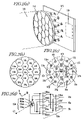
- FIG. 3 is a schematic configurational diagram of the deformable mirror 8 in this embodiment.
- the deformable mirror 8 in this embodiment comprises a substrate 21 , a reflective film (reflector) 32 which is supported by the substrate 21 and the shape of whose reflective surface is variable, and a plurality of drive units (actuators 33 ) for driving a plurality of regions of the reflective film 32 independently and thereby controlling the distances between the plurality of regions and the substrate 21 .
- actuators 33 a plurality of drive units for driving a plurality of regions of the reflective film 32 independently and thereby controlling the distances between the plurality of regions and the substrate 21 .
- the reflective film 32 functioning as a reflector has a plurality of light reflecting areas which can be individually driven.
- the reflector of the deformable mirror according to the invention can as well be configured of a plurality of micromirrors separated from one another. In this case, the mirror face of each micromirror functions as a light reflecting area.
- An embodiment of the present invention such a type of deformable mirror will be described in detail afterwards.
- Each of the actuators 33 includes a first fixed electrode 29 and a second fixed electrode 29 ′ provided over the substrate 21 , a rotating member (yoke 28 ) rotating around an axis of tilt, and an action member (coupling stub 30 a ) which varies the distance between a specific region of the reflective film 32 and the substrate 21 according to the motion of the yoke 28 .
- the yoke 28 has a supporting portion (supporting post 27 ) arranged on the axis of tilt and a planar portion coupled to the supporting post 27 .
- the planar portion has a first electroconductive portion (first portion 28 a ) and a second electroconductive portion (second portion 28 b ), which are symmetric with respect to the axis of tilt.
- the first portion 28 a and the second portion 28 b of the yoke 28 are respectively opposite the first fixed electrode 29 and the second fixed electrode 29 ′ with a gap in-between.
- Each of the actuators 33 is coupled to the corresponding region of the reflective film 32 , and can bidirectionally drive the position of a prescribed region of the reflective film 32 .
- the prescribed region of the reflective film 32 is coupled to either the first portion 28 a or the second portion 28 b of the corresponding yoke 28 by a coupling stub 30 a extending from the reflective film.
- the prescribed region of the reflective film 32 can be displaced by a stroke action in a direction substantially normal to the substrate. As the length of this stroke is no more than about twice the wavelength of the light, the phase of the reflected light can be modulated with a high degree of accuracy.
- the circumference of the reflective film 32 is formed of a deformable film fixed to the substrate 21 , and the reflective film 32 is given a tensile force in advance. For this reason, when the first fixed electrode 29 and the second fixed electrode 29 ′ become equal in electric potential, the reflective film 32 promptly returns to its original flat shape.
- the substrate 21 is formed from a silicon wafer, and a CMOS drive circuit 22 is integrated over the substrate 21 .
- FIG. 3 shows only the block configuration of the drive circuit 22 , but does not shown any specific sectional configuration of the n-channel MOSFET and the p-channel MOSFET constituting the CMOS.
- Al aluminum
- an insulating layer 24 is typically shown.
- insulating layer 24 is made of an SiO 2 -based or SiN-based material.
- the upper face of the insulating layer 24 is planarized by chemical mechanical polishing (CMP).
- the insulating layer 24 comprises openings (via holes) for bringing into electrical contact the electrodes above and the interconnection layer 23 underneath with each other.
- FIG. 3 illustrates only three actuators positioned near the periphery 26 of the substrate for the sake of simplicity.
- FIG. 4 is an exploded perspective view of the actuators 33 and the reflective film 32 in this embodiment of the present invention.
- the actuators 33 in this embodiment of the present invention have a base 34 formed over the insulating layer of the substrate not shown in FIG. 4 .
- the base 34 is formed of the same material as the first and second fixed electrodes 29 and 29 ′, and preferably should be fabricated together with the first and second fixed electrodes 29 and 29 ′ by patterning a film of metal, such as Al.
- the base 34 comprises supporting post fitting portions 34 a represented by one-dot chain lines and yoke contacting portions 34 b and 34 b ′ which come into contact with the yoke 28 when it has rotated to the maximum. This arrangement prevents the yoke 28 from coming into contact with the first and second fixed electrodes 29 and 29 ′.
- the first fixed electrode 29 and the second fixed electrode 29 ′ are provided in substantially symmetric positions around the tilt axis A of the yoke 28 formed by a supporting post 25 .
- the yoke 28 has a substantially planar shape, and is connected to the supporting post 25 via a hinge portion 28 b .
- the yoke 38 is rotatable a round the tilt axis A by a torsional deformation of the hinge portion 28 b.
- the yoke 28 has the first portion 28 a and a second portion 28 a ′ divided into right and left opposing positions with the tilt axis A in-between, the first portion 28 a in a position opposite the first fixed electrode 29 with a gap between them and the second portion 28 a ′ in a position opposite the second fixed electrode 29 ′ with a gap between them.
- the yoke 28 is also coupled to the coupling stub 30 a at a yoke free end 28 c represented by one-dot chain lines.
- the yoke free end 28 c is within the area of the first portion 28 a of the yoke 28 and in a position at a prescribed distance from the tilt axis A. As will be described afterwards, this distance can be differentiated from one actuator to another.
- the yoke 28 and the supporting post 25 can be formed by etching the same Al layer. Since the yoke 28 and the supporting post 25 , as well as the base 34 , are electroconductive and, moreover, electrically connected to one another, the electric potential of the yoke 28 is the same as that of the base 34 .
- the reflective film 32 in this embodiment of the present invention comprises a base film 30 made of an SiO 2 -based or an SiN-based insulator and a reflective layer 31 of an Al or Au material formed over its upper face.
- the reflective layer 31 can be fabricated by vapor-depositing a thin layer of metal over the base film 30 .
- the coupling stubs 30 a formed in the same film formation process as the base film 30 , have a function to couple the base film 30 to the yoke 28 . Elsewhere than in the positions where the coupling stubs 30 a are provided, a gap is provided between the yoke 28 and the base film 30 . The presence of this gap can prevent the base film 30 and the yoke 28 from coming into direct contact with each other elsewhere than the positions of the coupling stub 30 a even though the yoke 28 rotates.
- the gap between the yoke 28 and the base film 30 and that between the yoke 28 and the first and second fixed electrodes 29 and 29 ′ are produced in the following manner, for instance.
- the sacrificial layers are removed at the final step by plasma etching or otherwise.
- the reflective surface of the base film 30 is planarized by CMP before these sacrificial layers are removed.
- the first portion 28 a is attracted by an electrostatic force in the direction of approaching the first fixed electrode 29 with the result that the yoke 28 rotates in the counterclockwise (CCW) direction around the tilt axis A.
- the second portion 28 a ′ is attracted by an electrostatic force in the direction of approaching the second fixed electrode 29 ′, and the yoke 28 rotates in the clockwise (CW) direction around the tilt axis A.
- the tilts of the yoke 28 in the CCW direction and in the CW direction are transmitted via the coupling stub 30 a as driving forces to drive the reflective film 32 upwards and downwards; the reflective film 32 is provided to be deformable bidirectionally, in the direction of approaching the substrate and in the direction of moving away from the substrate.
- the yoke 28 comprises the first portion 28 a and the second portion 28 a ′ separated into opposing position with the tilt axis A in-between and, moreover, the first fixed electrode 29 is opposed to the first portion 28 a while the second fixed electrode 29 ′ is opposed to the second portion 28 a ′. Furthermore, the first portion 28 a is coupled to the reflective film 32 via the coupling stub 30 a .
- the use of this configuration makes it possible to bring prescribed regions of the reflective film 32 close to the substrate 21 or away from the substrate 21 , and to actively drive bidirectionally a plurality of localized regions of the reflective surface 3 . In this manner, this embodiment of the present invention can provide a deformable mirror having a high degree of symmetry of drives and excelling in control accuracy and responsiveness.
- the reflective film 32 holds a reflective fact having a high degree of planar accuracy obtained by the machining for CMP.
- the position of the reflective surface in the neutral state described above is deemed to be the neutral point, and the position of the reflective surface is driven bidirectionally with respect to this neutral point.
- the yoke contacting portions 34 b and 34 b ′ prevent the yoke 28 from coming into contact with the first and second fixed electrodes 29 and 29 ′, short-circuiting between them can be prevented without fail.
- FIG. 3 is referred to again.
- the yoke 28 is connected to the interconnection layer 23 by way of the supporting post 27 and via holes 25 , and the electric potential of the yoke 28 when in operation is always kept at the ground potential (hereinafter this electric potential will be referred to as “L”) all the time.
- L ground potential
- the electric potential of the first fixed electrode 29 is controlled to V 0 and that of the second fixed electrode 29 ′, to V 1 .
- the electric potentials of the first and second fixed electrodes 29 and 29 ′ can be switched between the ground potential L and a relatively high electric potential (electric potential H) by the drive circuit 22 .
- the “relatively high electric potential” can be set to, for instance, 5 V. Only one of the electric potentials V 0 and V 1 is controlled to the electric potential H.
- the yoke 28 is attracted by an electrostatic force towards the fixed electrode of the electric potential H with the result that a rotational force generates in the clockwise or the counterclockwise direction.
- the magnitude of the rotational force can be adjusted by controlling the length of time during which a state of H in electric potential is maintained at a plurality of levels (256 steps) expressed in eight bits. When no rotational force is let generate, the electric potentials V 0 and V 1 are set to the electric potential L.
- the gap between the base film 30 and the yoke 28 and the gap dg between the yoke 28 and the first and second fixed electrodes 29 and 29 ′ is set to about 2 trough 15 ⁇ m each.
- the designed width of the gap dg is set to 5 ⁇ m for both.
- the designed thickness in this embodiment of the present invention is 1.2 ⁇ m.
- the thickness of the reflective film 31 is set to, for instance, 0.1 ⁇ m or less.
- the drive circuit 22 receives the address Ain of each fixed electrode of each actuator and control data Din expressing driving force, and performs time control over H/L of the output voltages V 0 trough V 59 of each fixed electrode.
- the drive circuit 22 is configured of a memory 35 , an address counter 36 , a counter 37 , a comparator 38 , a shift register 39 and a latch 40 .
- the address counter 36 gives six-bit addresses to the memory 35 , and causes 60 sets of control data to be sent out serially.
- the address counter 36 is reset with an initialization (clr) signal, and counted up with a clock (clk) signal.
- the counter 37 is an eight-bit incremental counter which is reset with an initialization (clr) signal and counted up with a strobe (stb) signal after having read 60 sets of control data.
- the comparator 38 compares the output of the counter 37 with the eight-bit data of the memory 35 , and sends out to the shift register 39 one-bit serial data. If the data of the memory 35 are found greater than the output of the counter 37 , it will output 1 (H) or otherwise 0 (L).
- the shift register 39 is a 64-bit shift register operating in response to a clk signal, and validly uses 60 of the 64 bits.
- the latch 40 is a 64-bit latch which latches the value of the shift register 39 in response to a stb signal and, like the shift register 39 , validly uses 60 bits.
- This drive circuit 22 will be described. Eight-bit control data written in the memory 35 are read out, the 64 sets (of which 60 are valid) consecutively, according to six-bit addresses given by the address counter 36 .
- the address counter 36 has completed a round and all the control data in the memory 35 have been read, data accumulated in the shift register 39 are stored into the latch 40 in response to an stb signal, the output of the counter 37 is counted up at the same time, and the contents of the memory 35 are read out again from the beginning.
- This cycle being denoted by T, constitutes the minimum unit of the duration of electricity flow to the actuator.
- the control over the duration of electricity flow is accomplished by repeating this cycle T 256 times, which is determined by the number of steps of the counter 37 .
- each output of the comparator 38 becomes 0 as the corresponding output of the memory 35 becomes no greater than the count of the counter 37 because the count of the counter 37 increases every cycle. Therefore, the output of the latch 40 has come to permit control of the duration of electricity flow to the fixed electrodes of all the actuators at the minimum resolution T in proportion to the inputted control data Din.
- the ratio of the electricity flow duration Din ⁇ T to the control cycle 256 ⁇ T will be referred to as the electricity flow duration duty U, and U takes a value in the range of 0 trough 255/256.
- FIG. 5 are plans of the deformable mirror 8 in this embodiment of the present invention.
- FIG. 5( a ) Thirty points represented by black dots 8 a trough 8 ad are the drive points of the actuators.
- the drive points of the actuators correspond to the positions of the coupling stubs ( 30 a in FIG. 3) , the points where the reflective film is actually driven up or down.
- the x marks represent the positions corresponding to the 19 quadrisected photodetectors described with reference to the optical detector array, and are shown here as supplementary information. While only three points 15 a , 15 b and 15 s , which are to be taken up again in the subsequent description of the operation, are assigned reference numbers here to avoid complicating the illustration, they are arranged in positions reverse to those shown in FIG.
- the drive points 8 a trough 8 f are at the vertexes of a hexagon circumscribing a circle of the radius r 1 around the origin O, and the middle point between two adjoining vertexes substantially coincides with the central point of a quadrisected detector marked with x.
- the drive points 8 g trough 8 r are at the vertexes of a dodecagon circumscribing a circle of the radius r 2 around the origin O, and the middle point between two adjoining vertexes substantially coincides with the central point of a quadrisected detector marked with x.
- the 12 drive points 8 s trough 8 ad are configured on a circle of the radius r 3 around the origin O.
- the surface shape of the reflective film 32 is set.
- the reflective film 32 is integrated with the substrate on the circular periphery 26 and in an infinitesimal area near the origin O, and its displacement is thereby regulated.
- the radius r 3 here is set to a greater value than the radius of the light beam coming incident on the deformable mirror. The reason is to minimize the impact of the condition of displacement restriction by the fixation of the reflective film 32 on the periphery 26 upon the correction accuracy of the wave front phase. Further, there are bored holes 32 a in the reflective film 32 near the periphery 26 . They can serve to reduce the deterioration of correction accuracy due to the condition of restricting the displacement of the periphery 26 .
- the reflective film 32 comprises many small holes 32 b of 1 trough 2 ⁇ m in radius in order not to cause a significant drop in the luminous energy of the reflected light beams.
- the presence of the small holes 32 b provides the following two advnatagous effects.
- a first advantageous effect is improvement in control responsivity.
- the small holes 32 b constitute ventilation ports for air, the effect of the air around the reflective film 32 to obstruct the shifting of the reflective film 32 can be alleviated.
- a second advantagous effect is improvement in the productivity of the etching process as the small holes 32 b disperse the etchant inflow paths.
- the small holes 32 b work together with the holes 32 a to function as inlet holes for the etchant, effects to prevent incomplete removal of the sacrificial layer and to reduce the length of time required for the etching process can be achieved.
- FIG. 5( b ) shows a layout of planar arrangement of the actuators; this illustrated state corresponds to the state shown in FIG. 5( a ) minus the reflective film 32 .
- the actuators 33 a trough 33 ad are substantially rhombic, and have exactly the same dimensions and shape to one another except in the positions of the drive points 8 a trough 8 ad of the respective actuators.
- the shapes of the fixed electrode, the supporting post and the yoke are equal among the actuators.
- the vertical angles of the rhombus are substantially 60 degrees at acute vertexes and substantially 120 degrees at obtuse vertexes. Such a shape enables the actuators to be efficiently arranged when six of them are disposed around the origin O.
- the distance from the rotational center of the actuator to the drive point represented by a one-dot chain line is supposed to be set to L 1 in the actuators 33 a trough 33 f on the inner circumference, L 2 in the actuators 33 g trough 33 r on the middle circumference and L 3 in the actuators 33 s trough 33 ad on the outer circumference.
- L 1 ⁇ L 2 ⁇ L 3 holds.
- the range of displacement setting for the actuators is made variable by individually setting the distance from the axis of tilt to the drive point for each actuator instead of fixing it. It is relatively easy to provide each individual actuator a different planar shape because its planar shape is determined by the pattern of the mask in the manufacturing process for the actuators, which are fabricated as micromachines in this embodiment of the present invention.
- the dimension in the direction of the film thickness because of the nature of the process, is difficult to differentiate from one actuator to another. Therefore, where the range of displacement setting in the direction of the film thickness of the actuator is to be determined by the film thickness of the sacrificial layer, it is inevitable to set every actuator in the same range.
- the rotational motion of the actuator is converted into a motion to displace the distance from the substrate. For this reason, it is possible to set the displacement range of the distance from the substrate for each actuator by differentiating the distance from the rotational center of the actuator to the drive point.
- the reflective film 32 is fixed to the substrate in the vicinity of the origin O.
- the deformable mirror can control the shape of the reflective surface with high accuracy by smoothly deforming the reflective film 32 with reference to this origin O. For this reason, it is preferable for the displacement of the actuators towards the inner circumference closer to the origin O to be smaller and that of the actuators towards the outer circumference farther from the origin O to be greater, and this condition is met in this embodiment of the present invention by setting the aforementioned relationship of L 1 ⁇ L 2 ⁇ L 3 .
- FIG. 6 are diagrams for describing the action to deflect light beam wave fronts in Embodiment 1 of the present invention.
- the wave fronts of the backward emitted beams P i.e. the equi-phase surface of the electric field constitutes, in an overall outlook, a curved surface of a higher order consisting of a plane wave augmented with aberration components, it is possible to perform approximation in which that curved surface is divided into a plurality of localized units and higher-order components are ignored in each individual localized unit.
- the actual surface of the reflective film 32 is two-dimensional, it is necessary to control the local inclinations ⁇ of the two orthogonally crossing directions.
- the radial direction and tangential direction of the circle are selected as the two orthogonally crossing directions to match the divided shape of the quadrisected photodetectors of the optical detector array.
- This relationship between the two-dimensional inclination of the reflective film 32 and the displacements of the drive points will be explained with reference to FIG. 5( a ).
- the displacements of the reflective film 32 at the drive points 8 a trough 8 ad will be represented by Za trough Zad, respectively.
- the displacements Za trough Zad are zero, the reflective film 32 is substantially on the same plane at the drive points 8 a trough 8 ad , the origin O and all the points on the periphery 26 .
- the displacements Za trough Zad can take either positive or negative values; displacements in the direction towards the viewer of the drawing are supposed to be positive, and displacements in the direction towards behind the drawing, negative.
- a total of 38 values including radial direction components ⁇ ar trough ⁇ sr and tangential direction components ⁇ at trough ⁇ st are defined for the positions 15 a trough 15 s , marked with x, corresponding to the 19 quadrisected photodetectors as average inclinations near the x marks.
- the relationships among these displacements Za trough Zad and the radial and tangential local inclinations ⁇ ar trough ⁇ sr and ⁇ at trough ⁇ st will be described with respect to three typical points 15 b (inner circumference), 15 s (outer circumference) and 15 a (original) by way of example.
- the tangential direction ⁇ bt used here is the quotient of the difference in displacement between the drive points 8 d and 8 c by the distance between the two points as expressed in Equation 3.
- the radial direction ⁇ br used here is the average of the inclination formed by the middle point between the drive points 8 c and 8 d (i.e. the point 15 b itself) to the origin O and of the inclination formed by the middle point between the drive points 8 k and 8 l to the origin O as expressed in Equation 4.
- ⁇ t trough ⁇ gt and ⁇ cr trough ⁇ gr are given to the five other points 15 c trough 15 g on the inner circumference.
- ⁇ ⁇ ⁇ br - Zc + Zd 4 ⁇ r 1 - Zk + Zl 4 ⁇ r 2 ( Equation ⁇ ⁇ 4 )
- the tangential direction ⁇ st used here is the quotient of the difference in displacement between the drive points 8 n and 8 m by the distance between the two points as expressed in Equation 5.
- the radial direction ⁇ sr used here is the average of the inclination formed by the middle point between the drive points 8 m and 8 n (i.e. the point 15 s itself) to the drive point 8 z and of the inclination formed by the middle point between the drive points 8 d and 8 e to the drive point 8 z as expressed in Equation 6.
- ⁇ ht trough ⁇ rt and ⁇ hr trough ⁇ rr are given to the five other points 15 h trough 15 r on the outer circumference.
- ⁇ ⁇ ⁇ sr Zd + Ze - 2 ⁇ Zz 2 ⁇ ( r 3 - r 1 ) + Zm + Zn - 2 ⁇ Zz 2 ⁇ ( r 3 - r 2 ) ( Equation ⁇ ⁇ 6 )
- the tangential direction ⁇ at used here is the quotient of the difference in displacement between the drive points 8 d and 8 a by the distance between the two points as expressed in Equation 7.
- the radial direction ⁇ ar used here is the average of the inclination formed by the middle point between the drive points 8 b and 8 c to the origin O and of the inclination formed by the middle point between the drive points 8 e and 8 f to the origin O as expressed in Equation 8.
- ⁇ ⁇ ⁇ ar Ze + Zf - Zb - Zc 4 ⁇ r 1 ( Equation ⁇ ⁇ 8 )
- the relationships among these displacements Za trough Zad and the local inclinations Oar trough ⁇ sr and Oat trough ⁇ st are figured out. Further by expressing the wave front variations ⁇ of the backward emitted beams P in radial direction components ⁇ ar trough ⁇ sr and tangential direction components ⁇ at trough ⁇ st by using the same suffix expressions as for the local inclinations ⁇ , the relationships among the displacements Za trough Zad and the wave front variations ⁇ par trough ⁇ sr and ⁇ at trough ⁇ st can be figured by applying Equation 2.
- Equation 10 Equation 10
- the ratio Y/S between the difference signal and the sum signal can be approximated to a proportional relationship to the local wave front variations ⁇ .
- the difference signal/sum signal ratios Yar/Sa trough Ysr/Ss and Yat/Sa trough Yst/Ss of the 19 individual quadrisected photodetectors 15 a trough 15 s can be related to the local wave front variations ⁇ ar trough ⁇ sr and ⁇ at trough ⁇ st.
- Equation 2 trough Equation 11 and equivalent formulas whose statement is dispensed with, the difference signal/sum signal ratio Y/S of each quadrisected photodetector of the optical detector array is proportional to the local wave front variations ⁇ of the light beams P and, since these local wave front variations ⁇ can be expressed in a linear formula of the displacement Z of the reflective film 32 of the deformable mirror 8 , Y/S can be represented by a linear expression of Z by eliminating ⁇ from these equations.
- the driving forces of the actuators at the drive points 8 a trough 8 ad are represented by Fa trough Fad, respectively.
- the driving forces Fa trough Fad can take either positive or negative values; driving forces driving the reflective film 32 in the direction towards the viewer of the drawing are supposed to be positive, and driving forces in the direction towards behind the drawing, negative.
- a coefficient of a fixed value determined by the configuration of the reflective film 32 being represented by k, Equation 12 holds true of every the drive point as a basic idea.
- FIG. 7 are enlarged plans of the deformable mirror 8 in Embodiment 1 of the present invention. First will be explained the details of ⁇ Za/L regarding the drive point 8 a on the inner circumference with reference to FIG. 7( a ).
- Five points including the origin O and the drive points 8 b , 8 f , 8 g and 8 r will be taken up as points around the drive point 8 a , and the distances from these points to the drive point 8 a are supposed to be Lao, Lab, Laf, Lag and Lar, respectively.
- the angle resulting from equal bisecting of the angle formed by the drive points 8 r , 8 a and 8 g will be represented by a ⁇ 1 ; that resulting from equal bisecting of the angle formed by the drive points 8 g , 8 a and 8 b , by ⁇ 2 ; that resulting from equal bisecting of the angle formed by the drive point 8 b , the drive point 8 a and the origin O, by ⁇ 3 ; that resulting from equal bisecting of the angle formed by the origin O and the drive points 8 a and 8 f , by ⁇ 4 ; and that resulting from equal bisecting of the angle formed by the drive points 8 f , 8 a and 8 r , by ⁇ 5 .
- the average inclination between the drive point 8 g and the drive point 8 a is (Zg ⁇ Za)/Lag, and the angle of view ( ⁇ 1 + ⁇ 2 ) seen from the drive point 8 a approximates what this average inclination is applicable to. Considering other points around in the same way would give Equation 13.
- ⁇ ⁇ ⁇ Za L ⁇ 1 + ⁇ 2 2 ⁇ ⁇ ⁇ ⁇ Za - Zg Lag + ⁇ 2 + ⁇ 3 2 ⁇ ⁇ ⁇ ⁇ Za - Zb Lab + ⁇ 3 + ⁇ 4 2 ⁇ ⁇ ⁇ ⁇ Za Lao + ⁇ 4 + ⁇ 5 2 ⁇ ⁇ ⁇ ⁇ Za - Zf Laf + ⁇ 5 + ⁇ 1 2 ⁇ ⁇ ⁇ ⁇ Za - Zr Lar ( Equation ⁇ ⁇ 13 )
- All of Lao, Lab, Laf, Lag, Lar and ⁇ 1 trough ⁇ 5 are constants that can be figured out from the shape of the arrangement of the drive points, and can be represented by functions of r 1 and r 2 .
- the inclinations ⁇ Zb/L trough ⁇ Zf/L of the other drive points 8 b trough 8 f , respectively, on the inner circumference can be figured out in the same way.
- ⁇ Zg/L of the drive point 8 g on the middle circumference the way of thinking is exactly the same as concerning the drive point 8 a on the inner circumference.
- ⁇ Zg/L can be formulated by figuring out the distances between these points and the drive point 8 g and the angle of view seen from the drive point 8 g .
- the inclinations ⁇ Zh/L trough ⁇ Zr/L of the other drive points 8 h trough 8 r , respectively, on the middle circumference can be figured out in the same way.
- the angle formed by an end points P 1 and P 1 of the connecting portion 32 c between the two holes 32 a to the drive point 8 t will be represented by ⁇ 1 ; the angle formed by another end point P 3 and the drive points 8 t and 8 u , by ⁇ 1 ; that resulting from equal bisecting of the angle formed by the drive points 8 u , 8 t and 8 h , by ⁇ 3 ; that resulting from equal bisecting of the angle formed by the drive point 8 h , 8 t and 8 g , by ⁇ 4 ; that resulting from equal bisecting of the angle formed by the drive points 8 g , 8 t and 8 s , by ⁇ 5 ; and that formed by the drive points 8 s and 8 t and still another end point ⁇ 4 , by ⁇ 6 .
- Lt, Ltu, Lth, Ltg, Lts and ⁇ 1 trough ⁇ 6 like the drive points on the inner circumference, are constants can be figured out from the shape of the arrangement of the drive points, and can be represented by functions of r 2 and r 3 .
- the inclinations ⁇ Zu/L trough ⁇ Zad/L of the drive points 8 u trough 8 ad , respectively, on the outer circumference can be figured out in the same way.
- the driving forces Fa trough Fad of the actuators can be represented by the linear expressions of displacements Za trough Zad including the accelerations d 2 (Za)/dt 2 trough d 2 (Zad)/dt 2 of the drive points, the velocities d(Za)/dt trough d(Zad)/dt of the drive points, and the drive points around.
- the flow duration duty U is the quotient of the duration of electricity flow in the H state by the control cycle as described with reference to FIG. 3 .
- a fixed electrode 29 (or 29 ′) and a yoke 28 constitute a capacitor, whose electrostatic capacitance Ca is a function of its own displacement Z represented by the approximation of Equation 15, where ⁇ 0 is a vacuum dielectric constant; S, an effective area; and k′ is a positive constant of not greater than 1.
- the driving force F is approximated by Equation 16 as the product of multiplication of the partial differential of electrostatic energy CaV 2 /2 in the distance direction by the flow duration duty U.
- the time constant CaR which is the product of the electrostatic capacitance Ca and the resistance R of the current path, is great and shifting the electric charge takes time, the nonlinearity of F and U is great, but in any case it is possible to give the driving force F as a function of the flow duration duty U of the drive voltage for the fixed electrodes and of the displacement Z according to the drive direction.
- F ⁇ - ⁇ 0 ⁇ S ⁇ ⁇ V 2 ( d ⁇ ⁇ g ⁇ k ′ ⁇ Z ) 2 ⁇ U ( Equation ⁇ ⁇ 16 )
- the efficiency of computation needed for control is enhanced by using a method by which the relationship from the driving force to the output of the optical detector array is first figured out in a linear matrix expression and after that the driving force is individually converted into a flow duration duty on a nonlinear basis.
- the state vector x of the deformable mirror 8 is a column vector having 60 components including the displacements Za trough Zad and velocities d(Za)/dt trough d(Zad)/dt.
- x [ Za , Zb , ... ⁇ , Zad , d Za d t , d Zb d t , ... ⁇ , d Zad d t ] T ( Equation ⁇ ⁇ 18 )
- the driving force vector f of the actuator is a column vector having 30 components including the driving forces Fa trough Fad.
- f [fa, Fb, . . . , Fad] T (Equation 19)
- Equation 21 gives d, which is a disturbance vector, which is a column vector having 38 components generated by the wave front aberrations of the disk and other causes, and is subject to correction control.
- d [Dar, Dat, Dbr, Dbt, . . . Dsr, Dst] T (Equation 21)
- Matrix A is a 60 ⁇ 60 type matrix function
- matrix B is a 60 ⁇ 30 type one
- matrix C is a 38 ⁇ 60 type one
- the components of matrixes A, B and C are determined by Equation 2 trough Equation 14 already explained and equivalent formulas whose explanation has been dispensed with.
- the components of matrixes A, B and C contain many zeros and, to indicate this, expressions using submatrixes are represented by Equation 24 trough Equation 26.
- A [ A 1 0 ⁇ 1 I ] (Equation 24)
- B [ ⁇ 2 0 ] (Equation 25)
- C [C 1 0] (Equation 26) where 0 is a zero matrix; I, a 30 ⁇ 30 type unit matrix; A 1 , a 30 ⁇ 30 type non-diagonal matrix; ⁇ 1 , and ⁇ 2 , 30 ⁇ 30 type diagonal matrixes; and C 1 , a 38 ⁇ 30 type non-diagonal matrix.
- a vector x as indicated by Equation 27, consists of a displacement vector Z and a velocity vector V.
- X [ Z V ] ( Equation ⁇ ⁇ 27 )
- the purpose of wave front phase control is, if any disturbance d is cause to arise by a disk tilt, a variation in base thickness or the like, to provide appropriate driving forces f to the actuators of the deformable mirror, thereby vary the state x of the mirror to achieve conversion so that the output y be always a zero vector.
- the configuration to realize this control operation will be described with reference to FIG. 8 .
- FIG. 8 is a schematic configurational diagram of the control unit in Embodiment 1 of the present invention.
- the control unit 50 is configured of a target setting unit 51 , a steady deviation control unit 52 , a stabilizing compensation unit 53 and an f/u conversion unit 56 ; the output vector y of the wave front phase detector 16 is inputted, and the flow duration duty vector u of the actuator is outputted.
- the target setting unit 51 sets a target vector yr which serves as the target of the output vector y of the wave front phase detector 16 .
- the target vector yr is set to a zero vector.
- the target setting unit 51 carries out feed forward control by setting the target vector yr to that estimated vector.
- the method of setting the target vector yr in switching the in-focus layer of a two-layered optical disk will be described.
- the standard variation ⁇ d of the disturbance vector d arising at the time of an inter-layer jump is preset in an ROM.
- the target vector yr is set to a value calculated back in such a way that the predicted variation in the output vector y coincide with ⁇ d when the system is subjected to open loop control only for a prescribed length of time tj.
- the required length of time tj is set to a relatively large value in order to prevent overshooting, which is the length of time the objective lens requires to shift its focus, i.e. two to three times as long as the standard length of time taken from the time the shifting is started until the address of the header portion of another layer is read out.
- a predetermined value is set in an ROM.
- the steady deviation control unit 52 is an integral compensator configured to coupling p integrators in series, multiplying the outputs of the respective integrators by gain matrixes K 1 trough Kp and adding the resultant products in order to realize the number of types p required to comply with an error signal yr-y with no steady deviation.
- the number of types p and the values of the gain matrixes K 1 trough Kp are figured out in the design process in accordance with the relationship between the degree of the function of the vector y to be responded to and the matrix functions A, B and C, and set as predetermined functions.
- the stabilizing compensation unit 53 is a differential compensator for stabilizing a closed loop system asymptotically, and is configured here of an observer 54 and a regulator 55 .
- the observer 54 is a least-dimensional observer, to which the output vector y of the wave front phase detector 16 and the driving force vector f of the actuator are inputted, for outputting an estimated value x′ of the state vector x.
- the regulator 55 outputs the result of linear computation of the estimated state vector x′, which is inputted, according to a feedback gain matrix F. Values designed in advance so that the poles of the closed loop system be arranged in appropriate positions of a complex left plane to be stabilized asymptotically are set in the matrix F.
- the sum of the addition of the output the regulator 55 and the output of the steady deviation compensation unit 52 is the driving force vector f of the actuator.
- the f/u conversion unit 56 is a nonlinear conversion unit for converting the driving force vector f of the actuator into the flow duration duty vector u, which is the actual control signal.
- To the f/u conversion unit 56 are inputted driving force vector f and the estimated state vector x′, and the flow duration duty U is figured out with respect to 30 components corresponding to the individual actuators from the estimated values of the driving force F and the displacement Z in accordance with Equation 16.
- the f/u conversion unit 56 has a selector circuit for selecting either one of the two fixed electrodes each actuator has and a conversion table in which are stored values predetermined as nonlinear functions in a memory.
- the configuration is such that first the fixed electrode to be driven is selected according to the positive or negative sign of the driving force F, and then the flow duration duty U is obtained by inputting Z and F to the conversion table as addresses. This procedure is performed for the 30 actuators, and the flow duration duty vector u is obtained.
- the control unit 50 constitutes a closed loop system together with the deformable mirror 8 and the object of control of the wave front phase detector 16 mentioned above.
- the flow duration duty u is inputted to the deformable mirror 8 , and first the actuators 33 generate driving forces f.
- the state x of the reflective film 32 is varied by the driving forces f, and the wave front phase of the reflected light beams is thereby changed to vary the output y of the wave front phase detector 16 .
- the wave front phase of the light beams is also changed by a disk tilt, a variation in base thickness, sticking of a fingerprint or the like, and these affect the output y as the disturbance d.
- the control unit 50 outputs the flow duration duty u, corrects it in compliance with variations in the disturbance d, and performs control so as to keep the output vector y at zero all the time.
- the optical disk 10 is fitted to a disk motor (not shown) and rotated, and focusing of the objective lens 9 and tracking control over the target track are carried out.
- no drive voltage is given to the deformable mirror 8 as yet, and the mirror surface is flat, with no correction of the wave front phase being performed.
- the information recording device counts clock signals prepared from the VFO signals, and samples the output of the wave front phase detector 16 at a timing when the beam spot 17 is within the mirror portion 10 b.
- a control unit (not shown) sets the target vector yr to a zero vector, generates the flow duration duty u to the deformable mirror 8 so as to make this sampled output y zero, and performs control to correct the wave front phase by varying the shape of the mirror.
- the configuration is such that, in case of failure to validly sample the output of the wave front phase detector 16 on account of a failure in address reading or the like, the previous valid output can be held as it is. In this way, the detection of the wave front phase by the wave front phase detector 16 takes place in a state in which the beam spot 17 is securely within the mirror portion 10 b , and accurate wave front phase detection can be accomplished without being affected by any pre-pit or groove.
- the control band of the objective lens 9 is set sufficiently higher than the control band of the deformable mirror 8 in a configuration that can suppress deterioration in the accuracy of wave front phase detection due to control errors of the objective lens 9 .
- a rough seek is performed in a state in which the last valid output of the wave front phase detector 16 in the seek start position is held, and the output the wave front phase detector 16 is sampled from the mirror portion 10 b in which an address was first read in to control wave front phase correction.
- the target vector yr remains at a zero vector. If a state in which no address can be read after the rough seek continues for a prescribed length of time or longer, all the drive voltages to the deformable mirror 8 are reduced to zero, and the seek source is once released from its corrected state and the address reading action is tried again.
- the control unit first holds the last valid output vector y of the wave front phase detector 16 on the first layer, and then the target setting unit sets a prescribed target vector yr. Since a non-zero target vector yr is given with the output vector y held, error vectors yr-y increase and, along with a variation in the flow duration duty u to the deformable mirror 8 , the state vector x of the deformable mirror 8 is forcibly varied, and feed forward control is performed by an open loop in the direction of correcting wave front aberrations.
- the target setting unit After the address of the second layer is read in, the target setting unit again sets the target vector yr to a zero vector, and the last valid output vector of the wave front phase detector 16 on the first layer is released from the held state, and closed loop control is started on the basis of a newly sampled valid output vector of the second layer.
- the target setting unit By performing feed forward control by having the target setting unit provide an appropriate target vector yr where the occurrence of any wave front aberration is predictable, prompt control of wave front phase correction can be accomplished with little transient error.
- the target setting unit again returns the target vector yr to a zero vector after the lapse of the prescribed length of time tj, and interrupts the forced variation of the state vector x of the deformable mirror 8 . After preventing a hang-up in this way, address reading is tried again.
- the target vector yr is held at a zero vector, and the deformable mirror 8 is controlled by the closed loop system which the control unit 50 constitutes so that the output vector y of the wave front phase detector 16 be kept at a zero vector all the time even if there is a disturbance d.
- Equation 22 trough Equation 27 can be simplified like Equation 28 and Equation 29.
- f ⁇ 2 ⁇ 1 A 1 z (Equation 28)
- y C 1 z+d (Equation 29)
- Equation 30 is obtained from Equation 28 and Equation 29.
- f ⁇ 2 ⁇ 1 A 1 C 1 ⁇ ( y ⁇ d ) (Equation 30)
- Equation 29 itself is a formula which does not necessarily have an actual solution on account of a modeling error, measurement noise or the like, C 1 does exist, and it is possible to compute a displacement vector z that can give the optimal approximation, such as the above-mentioned.
- Equation 12 trough Equation 27, which constitute the basis of this approximation, cannot state wave front information on the whole backward light in such a simple expression, it is apparent that computation to reconstruct wave front information on the whole backward light is conducted.
- the wave front detector 16 detects local wave fronts of backward light and the control unit outputs to the deformable mirror 8 drive signals for reconstructing wave front information on the whole backward light on the basis of this detector output
- detection and correction of wave front aberrations can adapt to any wave front abberation instead of being limited to any specific type, and accurately correct complex wave front aberrations resulting from tilts, fluctuations in disk substrate thickness, double refraction, smear with fingerprints and the like.
- the areas of the individual lenses of the lens array 14 are made unequal and, in particular, the square measures of detection regions arranged in parts where the intensity of backward light is greater are made stronger than those of detection regions arranged in parts where the intensity of backward light is weaker, differences in condensed luminous energy from detector to detector ensuing from the uneven distribution of backward light intensity can be compensated for, and accordingly the accuracy of reconstruction of the whole wave fronts can be improved by uniformizing the S/N ratios of the output signals of individual optical detectors.
- the timing of detection by the wave front detector 16 is generated on the basis of the output of a medium information detecting part for detecting information stored by a medium, it is possible to securely detect wave fronts when the medium is in a suitable state for wave front detection, and accordingly accurate wave front phase detection can be accomplished.
- the yoke of the deformable mirror 8 has the first portion and the second portion separated to mutually opposite positions around the axis of tilt, with the first fixed electrode opposing the first portion and the second fixed electrode opposing the second portion, and the reflective film is coupled to the first portion via the coupling stubs, the reflective film can be actively driven in two directions, and the symmetry of the driving force can be improved to enhance control accuracy and responsiveness.
- the reflective film holds the reflective surface having a high degree of planar accuracy in a state in which no drive signal is given to either the first fixed electrode or the second fixed electrode, and bidirectional driving is performed with this state serving as the neutral point as it is, no initial deformation in advance to obtain the neutral point is required as according to the prior art, with the result that problems in the repeatability of the neutral point and the like due to fluctuations of drive sensitivity at the time of initial deformation and other causes, and accordingly the accuracy of correction can be improved.
- the setting range of displacement of the actuator can be made variable even if the dimension in the direction of film thickness is formed for every actuator in a uniform process.
- the displacements of actuators towards the inner circumference near the origin are set smaller, and the displacements of actuators towards the outer circumference farther from the origin are set greater, even if there is any erroneous operation in the control system over the actuators towards the inner circumference, the impact on the whole device can be suppressed because they are limited in displacement and, moreover the smaller range of displacement that is set facilitates improvement in actuator performance in terms of resolution and driving force, making possible highly response and accurate control.
- FIG. 9 shows a schematic configuration of this embodiment of the present invention.
- the deformable mirror 8 according to this embodiment of the present invention has the same configuration as that described with reference to Embodiment 1.
- the information device uses a plurality of light sources.
- a laser module 60 which integrates a photodetector and a GaN-based semiconductor laser of 405 nm in wavelength, which serves as a light source for a blue light recording disk.
- Blue light beams emitted from the laser module 60 are converted into parallel beams by a collimator lens 61 .
- a beam shaping prism 62 shape oval blue light beams into a circular shape.
- the shaped beams come incident on a polarization hologram 63 .
- the polarization hologram 63 which is a diffraction grating comprising a substrate of a birefringent material such as LiNbO 3 over which a hologram pattern is formed, does not provide any phase difference to extraordinary rays, but provide a phase difference to ordinary rays by adjusting refractive indexes in the groove parts of the pattern by proton exchange or otherwise.
- the polarization hologram 63 when being transmitted by the polarization hologram 63 , extraordinary rays are not diffracted, but ordinary rays are diffracted and deflected according to the hologram pattern.
- the groove depth is so designed to maximize the proportion of ⁇ 1st order beams for ordinary rays and to reduce that of zero-order beams substantially to zero.
- the extraordinary rays and the ordinary rays are linearly polarized beams polarized at a right angle to each other.
- the linearly polarized beams emitted from the polarization hologram 63 are converted into circularly polarized beams by a quarter-wave plate 64 , and brought to incidence on a dichroic prism 65 .
- the dichroic prism 65 comprises a blue light reflective surface 65 a and a red light reflective surface 65 b , and these surfaces selectively reflect or transmit beams according to the laser wavelength.
- the blue light reflective surface 65 a irrespective of the direction of polarization, almost totally reflect blue light of 405 nm in wavelength and almost totally transmit red to infrared light of 650 nm in wavelength.
- the red light reflective surface 65 b again irrespective of the direction of polarization, almost totally reflect infrared light of 780 nm in wavelength and almost totally transmit red to blue light of 650 nm in wavelength.
- the one other face is a usual face 65 c having no wavelength-selectivity.
- An the objective lens 67 made of a glass material having a high refractive index designed in a single lens configuration of 0.85 in NA.
- An optical disk 68 is provided to be able to accept a blue light recording disk, a DVD disk or CD disk permitting recording/reproduction by the laser module 60 and to record or reproduce thereon or therefrom.
- the blue light recording disk is a single-side two-layered recording disk provided with recording layers comprising a phase change recording material or dye-based recording material over a disk substrate of 0.6 mm in thickness, the two constituent substrates being stuck together with a transparent adhesive layer of 30 trough 50 ⁇ m in thickness in-between, and its format permits recording only in the grooves or on the lands.
- the groove pitch p i.e. the distance between adjoining grooves is prescribed as stated in Equation 32, so that the interference region between the zero-order and +1st order diffracted beams and the interference region between the zero-order and ⁇ 1st order diffracted beams of backward light in the grooves do not substantially overlap each other.
- the DVD laser module 69 is an integrated product of a GaInP/AlGaInP-based semiconductor laser of 650 nm in wavelength, which serves as the light source, and a photodetector.
- a lens 70 converts the red light beams emitted from the DVD laser module 69 into a finite optical system having a desired angle of expansion.
- a polarization hologram 71 has a similar configuration to the polarization hologram 63 .
- the polarization hologram 71 though not diffracting extraordinary rays, does diffract ordinary rays so as to maximize the proportion of ⁇ 1st order beams for ordinary rays and to reduce that of zero-order beams substantially to zero.
- Red light beams emitted from a quarter-wave plate 72 for converting linearly polarized beams into circularly polarized beams come incident, transmitted by the red light reflective surface 65 b of the dichroic prism 65 and, after being transmitted by the blue light reflective surface 65 a and emitted, are directed towards the deformable mirror 8 .
- the dichroic prism 65 performs the role of a beam shaping prism to shape oval blue light beams into circular beams.
- the CD laser module 73 is an integrated product of a GaAlAs-based semiconductor laser of 780 nm in wavelength, which serves as the light source, and a photodetector.
- a glass hologram 74 has a hologram pattern for making three beams for tracking control use on its face closer to the CD laser module 73 and, on the other face, another hologram pattern for deflecting backward light to the photodetector of the CD laser module 73 .
- a lens 75 converts light beams emitted from the CD laser module 73 into a finite optical system having a desired angle of convergence.
- FIG. 10 are schematic configurational diagrams of the laser module 60 and the polarization hologram 63 in this embodiment of the present invention.
- Blue light beams emitted from the light source 80 of the laser module 60 pass a collimator lens and a beam shaping prism not shown in FIG. 10 and come incident on the polarization hologram 63 .
- the polarization hologram 63 as shown in FIG. 10( b ), is divided into a total of 29 regions comprising 28 regions 63 a trough 63 ab for deflecting backward light to the photodetector and a region 63 xx for limiting the aperture to a certain size and in particular preventing backward light from returning to the light source. On each of these regions is formed the optimal diffraction grating pattern for deflecting backward light in each intended direction.
- the shapes of the regions 63 a trough 63 ab are designed in accordance with respective interference patterns formed by the grooves of the blue light recording disk.
- the regions 63 a , 63 n , 63 o and 63 ab correspond to the region of the zero-order reflected beams of the blue light recording disk.
- the regions 63 b trough 63 m correspond to the interference region between the zero-order reflected beams and the +1st order reflected beams, and the regions 63 p trough 63 aa correspond to the interference region between the zero-order reflected beams and the ⁇ 1st order reflected beams.
- the groove pitch p of the blue light recording disk is prescribed as stated in Equation 32, there is no interference region between the +1st order reflected beams and the ⁇ 1st order reflected beams, and no regions corresponding to the are provided on the polarization hologram 63 .
- Forward blue light beams having passed the polarization hologram 63 travel straight ahead without diffraction of extraordinary rays, but ordinary rays are diffracted and deflected.
- the deflected ordinary rays deviate out of the optical path to become invalid stray beams, and only extraordinary rays are reflected by the optical disk 68 as valid blue light beams to become backward light.
- backward light beams have become ordinary rays by passing a quarter-wave plate (not shown) twice, back and forth, almost the whole luminous energy is diffracted by the polarization hologram 63 , and ⁇ 1st order beams deflected to the photodetectors of the laser module 60 .
- the photodetectors of the laser module 60 consists of vertically divided photodetectors 81 bisected by a vertical dividing line corresponding to the recording track tangential direction of the blue light recording disk and horizontally divided photodetectors 82 bisected by a horizontal dividing line in a direction orthogonal thereto. There are 28 each of the vertically divided photodetectors 81 and the horizontally divided photodetectors 82 in a one-to-one correspondence to the respective regions 63 a trough 63 ab of the polarization hologram 63 .
- the hologram configuration regarding the focal position is not one of separating focal positions before and behind along the direction of the normal of the as is the usual practice by the SSD method, but one of positioning the focuses on the photodetector surface for both ⁇ 1st order beams.
- a relatively large spot diameter at the focus is provided, such as 50 trough 100 ⁇ m. This can be realized without strain because the division is very finely made into the 28 regions 63 a trough 63 ab , resulting in a small size of each region, and accordingly the NA as viewed from each photodetector is small. It will be explained afterwards that even such a configuration allows focusing error signals of the objective lens to be generated.
- L and R represent the left and right directions; U and D, the upward and downward direction; La trough Lab, the outputs of the left divided part of the vertically divided photodetectors 81 ; and Ra trough Rab, the outputs of the right divided part of the same.
- the small letters a trough ab respectively match the regions 63 a trough 63 ab of the polarization hologram 63 .
- Ua trough Uab represent the outputs of the upper divided part of the horizontally divided photodetectors 82 ; and Da trough Dab, the outputs of the lower divided part of the same.
- the outputs La trough Lab, Ra trough Rab, Ua trough Uab and Da trough Dab from the divided parts of the photodetectors are subjected to amplification, differential computation and adding computation by a preamplifier and a computing circuit (neither shown) to generate control signals and recording signals for the objective lens and the deformable mirror.
- a tracking error signal TE of the objective lens is generated as a luminous energy difference between right and left in the polarization hologram 63 by a push-pull method. Its contents are represented by Equation 33; where ⁇ ( ) is a sign denoting the total sum of the outputs in the parentheses.
- TE ⁇ ( La ⁇ L ⁇ ⁇ n , Ra ⁇ R ⁇ ⁇ n , Ua ⁇ Un , Da ⁇ Dn ) - ⁇ ( Lo ⁇ L ⁇ ⁇ ab , Ro ⁇ Rab , Uo ⁇ Uab , Do ⁇ Dab ) ( Equation ⁇ ⁇ 33 )
- FIG. 11 are diagrams for illustrating the principle of the relationship between focusing errors and the focal position on the photodetector in Embodiment 2.
- the explanation here is simplified by ignoring the effects of diffraction by the grooves in the optical disk and the like, but such a condition, if any, will make no difference to the basic concept. Also for the sake of simplification, the explanation refers to a one-dimensional mode, this can be easily expanded to a two-dimensional model.
- FIG. 11( a ) shows the positions of focusing on photodetectors in a state in which there are focusing errors in the direction in which the objective lens moves away from the optical disk.
- a wave front in which light beams 83 are in a state of parallel beams On the right-hand side of the drawing is typically shown a wave front in which light beams 83 are in a state of parallel beams. While a wave front W 0 in the absence of a focusing error is planar indicated by a one-dot chain line, a wave front W 1 in the presence of a focusing error as mentioned above presents a concave surface which is symmetric with respect to the optical axis as indicated by a solid line.
- regions of the polarization hologram 63 on which these parallel light beams 83 come incident are typically represented by wavy lines
- the distance between the center of each of these regions and the optical axis is represented by L.
- the distances L are predetermined values differing from region to region and, in an expansion to a two-dimensional model, constitute coordinates representing the central positions of the respective regions.
- the distances L may be either positive or negative, and here direction A in the drawing is supposed to be positive.
- This state is illustrated on the lefthand side of the drawing.
- the divided photodetectors can be treated in the same way, whether they are the vertically divided photodetectors 81 or the horizontally divided photodetectors 82 , and in the drawing a glimpse of dividing lines can be seen in the middle. Therefore, if FIG. 11( a ) is regarded as showing a view in the vertical direction, this will illustrate the vertically divided photodetectors 81 , or if it is regarded as showing a view in the horizontal direction, the horizontally divided photodetectors 82 .
- FIG. 11( b ) shows the positions, of focusing on photodetectors in a state in which there are focusing errors in the direction in which the objective lens approaches the optical disk.
- the constituent elements and signs in the drawing are the same as their respective counterparts in FIG. 11( a ).
- a wave front W 2 On the right-hand side of the drawing is shown a wave front W 2 in the presence of a focusing error as indicated by a solid line, and this presents a convex surface which is symmetric with respect to the optical axis.
- sign ⁇ denoting a deviation of the focusing position has a positive correlation with the sign of the distance L in this state, this correlation is due to the convex shape of the wave front W 2 .
- This value is stored in advance in a ROM as an offset value to be used as a compensator in computing the inclination k.
- a line having x marks plots a state corresponding to the wave front W 1 , i.e. a state in which there are focusing errors in the direction in which the objective lens moves away from the optical disk, and has a negative inclination k 1 indicated by a two-dot chain line.
- a line having; marks plots a state corresponding to the wave front W 2 , i.e. a state in which there are focusing errors in the direction in which the objective lens approaches the optical disk, and has a positive inclination k 2 indicated by a wavy line.
- a focusing error signal FE is generated by using an inclination k, and the objective lens is so controlled as to reduce this to zero after an offsetting correction.
- Generating focusing error signals in this way provides the following advantages over the prior art. While there are a number of focusing error detecting methods according to the prior art including the knife edge method, the SSD method and the astigmatism method, every one of them basically uses the whole wave front of backward light and detects focusing errors on the basis of variations in the curvature of this whole wave front. Thus, whereas the curvature of the whole wave front varies and the focal position shifts between before and behind the photodetector surface along with the movement of the objective lens towards or away from the optical disk, an optical design is contrived to detect this back and forth shifting of the focal position as a difference in divided photodetector output.
- the dividing line is so provided as to pass the optical axis and the luminous energy is made asymmetric; by the SSD method, and at the same time between the right and left of the dividing line; and by the astigmatism method, focal positions are also separated before and behind the photodetector surface according to the direction of the lens.
- Equation 34 The principle of the capability to generate focusing error signals FE is as explained above, and this is expressed in Equation 34 in a somewhat simplified way.
- Xa, Ya and Sa corresponding to the region 63 a are given as represented by Equation 35 trough Equation 37.
- signals for controlling the deformable mirror signals resulting from processing of the aforementioned output signals Xa trough Xab, Ya trough Yab and Sa trough Sab with a low pass filter will be used.
- the cut-off frequency of the low pass filter is set to a sufficiently lower value than the band of the reproduced signals of recording marks to avoid the effect of the modulation of the recording marks. It is even more preferable to set this cut-off frequency to a sufficiently lower value than the response frequency of the objective lens. The reason is that in this way wave front variation noises due to focusing errors and tracking errors can be averaged and thereby substantially reduce the effects of those noises.
- the output signals Xa trough Xab, Ya trough Yab and Sa trough Sab all mean such signals having undergone processing with the low pass filter.
- standardized outputs Xa/Sa trough Xab/Sab and Ya/Sa trough Yab/Sab are generated, a servo filter is figured out from state formulas in a matrix form as described with reference to Embodiment 1 of the invention, and the deformable mirror is so controlled as to make these outputs Xa/Sa trough Xab/Sab and Ya/Sa trough Yab/Sab to zero.
- the outer circumferential region 63 xx of the polarization hologram 63 performs the role of prescribing the aperture at a fixed value even if the angle of expansion from the light source 80 fluctuates, and the pattern of the hologram is so designed as to deflect ordinary rays in forward light outside the optical path to make them invalid stray light and, if transmitted extraordinary rays are reflected by the disk and come incident again as backward ordinary rays, to deflect them into positions where they would not affect the vertically divided photodetectors 81 and the horizontally divided photodetectors 82 .
- the detailed configurations of the photodetectors of the DVD laser module 69 and the polarization hologram 71 substantially the same as the contents described with reference to the laser module 60 and the polarization hologram 63 .
- the differences between them are little, if at all, than that the optical path of red light beams are composed of a finite system, beams are brought to incidence on the polarization hologram 71 in the oval form before they are shaped into a circular form and a difference in specific design dimensions corresponding to the difference in laser wavelength.
- the configurations of the photodetectors of the CD laser module 73 and the glass hologram 74 are basically the same as the contents described above.
- the differences from the configuration described above include a reduced number of localized areas into which the hologram pattern is divided for wave front phase detection on account of less exactness about the accuracy of correction, and the absence of a hologram pattern for wave front phase detection in positions where side beams are emitted or come incident with a view to compatibility with three-beam tracking detection.
- a glass hologram not a polarization hologram, is used, there is no difference in behavior attributable to the direction of polarization.
- Infrared light beams which are forward incident beams from the CD laser module 73 are first branched on the surface closer to the CD laser module 73 into three beams for tracking control use. Next, on the other surface, beams of the first and higher orders are deflected by a hologram pattern for deflection to photodetectors out of the optical path to become invalid stray light, and only zero-order beams are reflected by the optical disk 68 as valid infrared light beams to become backward light. Of the backward light beams, the +1st order beams are deflected by the photodetectors of the CD laser module 73 .
- the zero-order backward light beams, which feedback light to the semiconductor laser have no adverse effects, such as significant scooping, partly because of the relatively large quantity of feedback light.
- FIG. 12 are schematic diagrams of optical systems of information recording devices, differentiated by the disk type, in Embodiment 2 of the present invention.
- FIG. 12( a ) shows a blue light optical system for recording and reproducing onto or from blue light recording disks
- FIG. 12( b ) a red light optical system for recording and reproducing onto or from DVD disks
- FIG. 12( c ) an infrared optical system for reproducing from CD disks.
- the blue light optical system is an infinite system, while the red light optical system and the infrared optical system are finite systems; in particular, the infrared optical system is so disposed that the point of imaging by the lens 75 exist before the objective lens 67 , i.e. between the lens 75 and the objective lens 67 .
- the optical system of every color is so designed as to minimize wave front aberrations anticipated in the design in a state in which the deformable mirror 8 is not operated, i.e. in a state in which the reflective surface is flat.
- the finite red light optical system and infrared optical system are more subject to wave front aberrations due to deviations from the ideal design state, such as changes in focusing position resulting from lens shifting or face imbalance
- the stroke range of the actuators of the deformable mirror 8 is so prescribed that, even in the worst state of deviation, wave front aberrations at least may not go beyond the correctable range of the deformable mirror 8 .
- the optical disk 68 When the optical disk 68 is inserted by a loading mechanism and fitted to a disk motor (not shown), first the CD laser module 73 is caused to emit light, the objective lens 67 is shifted upwards for focusing, and it is judged whether or not the optical disk 68 is a CD disk. If the control track data of the optical disk 68 can be read and the optical disk 68 is judged to be a CD disk, the procedure shifts to the operation of usual CD reproduction. In any other case, the optical disk 68 is judged not to be a CD disk; next the DVD laser module 69 is caused to emit light for focusing, and it is judged whether or not the disk is a DVD disk.
- the procedure shifts to the operation of DVD recording/reproduction; in any other case, the optical disk 68 is judged to be a blue light recording disk, the laser module 60 is caused to emit light for focusing, and the procedure shifts to the operation of recording onto or reproducing from a blue light recording disk.
- the CD laser module 73 By causing the CD laser module 73 , the DVD laser module 69 and the laser module 60 to emit light in sequence and thereby identifying the type of the disk, it can be reliably prevent in the focusing operation the objective lens 67 from hitting against the optical disk 68 .
- the above-described operation is particularly effective where the following conditions hold.
- the collision focal distance f is defined as the distance from the disk surface to the focal point when the objective lens 67 has hit against the surface of the optical disk 68 .
- n is the refractive index of the disk substrate, which is given as a typical value 1.55 for polycarbonate resin, for example;
- r the pupil radius at the peak of the objective lens 67 , i.e. in its nearest position to the optical disk 68 , a value determined in the design of the optical system.
- the disk substrate thickness t of the optical disk 68 is greater than the collision focal distance f
- no detection can be done from the recording face of the disk, and in the focusing operation the objective lens 67 will hit against the surface of the optical disk 68 .
- the information recording device drives a laser module in accordance with the result of identification.
- the subsequent part of the operation is similar to what was described of the configuration and the contents of description of the operation of Embodiment 1 for the invention.
- the detected wave fronts are corrected with the deformable mirror 8 and recording/reproduction is carried out by using a common objective lens 67 , enabling interchanges among a plurality of types of optical disk 68 to be accurately accomplished with a simple configuration.
- various wave front aberrations including chromatic aberrations due to wavelength differences and spherical abberation ensuing from base thickness differences of the optical disk 68 are contained within a prescribed range by an appropriate optical design in advance, the remaining aberrations can be eliminated by wave front correction, making it possible to substantially enlarge the margins of designing against aberrations.
- the polarization hologram 63 deflects backward light in two directions differing from one to another of the regions 63 a trough 63 ab , and light is received by the vertically divided photodetectors 81 and the horizontally divided photodetectors 82 differing from each other in the direction of the dividing line, wave front components in two directions can be detected with effective utilization of diffracted beams, adjusting ease of detector positions, a low wiring density for outputs from the detectors and ease in wiring design.
- backward light is divided into a plurality of regions 63 a trough 63 ab according to the conditions of interference by the grooves of the optical disk 68 , and the conditions of interference are made substantially the same in the same region, accurate wave front detection can be accomplished even from backward light where the light intensity pattern is made complex by the interference of grooves.
- the accuracy of detecting focusing errors can be prevented from deterioration even if the detection regions of the polarization hologram 63 are multi-sected to reduce the area of each region. Also, the operation by the discrimination unit for the optical disk 68 to identify the disk type in the sequence of a CD disk, DVD disk and a blue light recording disk makes it possible to prevent the objective lens 67 from hitting against the optical disk 68 in the focusing action.
- FIG. 13 shows a schematic configuration of this embodiment of the present invention.
- common members with the first embodiment of the present invention are denoted by the same reference signs as their respective counterparts in FIG. 3 .
- the substrate 21 is formed of an Si material, whose thermal expansion coefficient is 2.8 trough 7.3 ⁇ 10 ⁇ 6 .
- a reflective film 83 is formed by sputter-vapor deposition of a metallic material having a greater thermal expansion coefficient than the substrate 21 . Where the material of the reflective film 83 is Al, its thermal expansion coefficient is about 23.6 ⁇ 10 ⁇ 6 .
- the reflective film 83 As the reflective film 83 is formed in a high temperature condition of about 450° C. and moreover is coupled to the substrate 21 at its periphery 84 , because of the difference in thermal expansion coefficient, the reflective film 83 behaves to contract more than the substrate 21 does at 80° C., which is the temperature condition of actual use, to create an internal stress in the direction of tension. This securely keeps the reflective film 83 under tension all the time, thereby enabling the planar accuracy of the reflective surface 85 a flattened by CMP to be maintained.
- Coupling stubs 83 b which couple the actuators 33 and the reflective film 83 to each other are formed of an Al material integrally with the reflective film 83 to establish electrical continuity between the yoke 28 and the reflective film 83 .
- the reflective film 83 is coupled the periphery 84 of the same Al material, and communicates with the interconnection layer 23 of the substrate 21 by way of via holes 85 bored in the insulating layer 24 , being dropped to the ground potential from the interconnection layer.
- FIG. 14( a ) schematically shows a section of the deformable mirror
- FIG. 14( b ) an exploded perspective view of actuators 94 and reflectors 93 .
- a substrate 86 , a interconnection layer 87 , an insulating layer 88 , and via holes 89 , 89 ′ and 89 ′′ have substantially the same configurations as the substrate 21 , the interconnection layer 23 , the insulating layer 24 , and the via holes 25 , 25 ′ and 25 ′′, respectively, in Embodiment 1, but are different in the positions of arrangement and some other respects.
- the configuration in this embodiment of the present invention differs from that in Embodiment 1 mainly in that the reflectors 93 consist of a plurality of micromirrors separated from one another, and an actuator 94 is coupled to each of the reflectors 93 .
- a base 95 in this embodiment of the present invention has a substantially rectangular shape of a length La and a width Wa.
- La and Wa determine the dimensions of a unit cell one actuator 94 occupies.
- Such a unit cell matches the area occupied by each actuator where the actuators 94 are laid with no blank space in-between, but is not identical with the dimensions of a yoke 91 .
- the length La and the width Wa of the actuators 94 will be used in this sense.
- the length La is set to be greater than the width Wa
- the lengthwise direction the actuators 94 crosses the tilt axis A orthogonally.
- the base 95 comprises supporting post fitting portions 95 a and yoke contacting portions 95 b and 95 b ′. Their functions are the same as their counterparts described with reference to Embodiment 1.
- the yoke 91 is connected to supporting posts 90 via hinge portions 91 b , and can be rotated round the tilt axis A by twist deformations of the hinge portions 91 b.
- the reflectors 93 operate independently of one another. It is possible to make the hinge portions 91 b as much more rigid than their counterparts in Embodiment 1 as the load which would otherwise result from the deformation of these reflectors 93 but are absent here.
- the yoke 91 has a first portion 91 a and a second portion 91 a ′ separated right and left with the tilt axis A in-between, and the first portion 91 a is in a position opposite a first fixed electrode 92 with a gap between them while the second portion 91 a ′ is in a position opposite a second fixed electrode 92 ′ with a gap between them.
- the yoke 91 is coupled to a coupling stub 93 b at a yoke's free end 91 c indicated by one-dot chain lines.
- the yoke's free end 91 c is within the region of the first portion 91 a of the yoke 91 , and positioned at a prescribed distance from the tilt axis A. As was stated with reference to Embodiment 1, this distance can be differentiated from actuator to actuator.
- the yoke 91 , the supporting posts 90 and the base 95 are all formed of an Al material and have the same electric potential.
- the reflectors 93 differ from the actuators 94 in the lengthwise direction, and are in a substantially rectangular shape having the tilt axis A as their lengthwise direction, with the width Wm greater than the length Lm.
- the reflectors 93 also formed of an Al material, are substantially rigid bodies, each having on its surface a reflective surface 93 a .
- the coupling stubs 93 b are formed in the same Al sputter-vapor deposition process as the reflectors 93 are.
- the reflectors 93 do not only move in purely vertical directions but also are inclined by the same angle as the inclination of the yoke 91 , the angle of inclination relative to the displacement can be kept very small because the shape of the actuators 94 has the direction normal to the tilt axis A as its lengthwise direction and the shape of the reflectors 93 has the direction of the tilt axis A as its lengthwise direction. Furthermore, the area Lm ⁇ Wa of the reflectors 93 is as large as 90% or more of the area La ⁇ Wa of the actuators to prevent the reflected luminous energy from decreasing.
- the width Wm of the reflectors is greater than the width Wa of the actuators, and the projective dimensions of the reflectors 93 are so provided as to partly overrun the dimensions of the actuators 94 .
- FIG. 15 is a diagram showing the arrangement of the actuators 94 and the reflectors 93 in Embodiment 4 of the present invention. Although each base 95 is depicted noticeably apart from the adjoining bases 95 in the drawing to make their boundaries readily recognizable, actually these gaps are either extremely narrow or zero.
- the length Lm and the width Wm of the reflectors 93 are determined to satisfy the conditions of Equation 40 and Equation 41. Lm ⁇ p (Equation 40) Wa ⁇ Wm ⁇ k ⁇ Wa (Equation 41)
- the length Lm and the width Wm of the reflectors 93 determined to satisfy these conditions make it possible suppress interference between the reflectors 93 themselves and their inclinations accompanying displacements in the vertical directions and at the same time to enhance the efficiency of reflection.
- the reflectors 93 consist of a plurality of micromirrors separated from one another and an actuator 94 is coupled to each of the reflectors 93 in this embodiment, the displacements of the reflectors 93 can be controlled for each actuator 94 in complete independence, and accordingly the control operation can be simplified and improved in responsiveness.
- FIGS. 16( a ) and 16 ( b ) show a schematic section of the deformable mirror
- FIG. 16( b ) shows an exploded perspective view of an actuator 104 and a reflector 105 .
- This configuration particularly differs from Embodiment 4 in that the reflector 105 is coupled at two points, i.e. the actuator 104 including a pair of yokes 101 and 102 and coupling stubs 105 a and 105 b , and thereby enable to shift up and down in parallel (in stroke actions).
- FIG. 16 details of supporting posts 100 and 110 , the yokes 101 and 102 , first fixed electrodes 106 and 107 , second fixed electrodes 106 ′ and 107 ′, a base 115 , a the substrate 116 , a interconnection layer 117 , an insulating layer 118 , via holes 119 , 119 ′ and 119 ′′ are substantially the same as what was described with reference to Embodiment 4.
- first and second fixed electrodes 106 and 106 ′ In positions opposite first and second portions 101 a and 110 a ′ of the yoke 101 are arranged the first and second fixed electrodes 106 and 106 ′, and in positions opposite first and second portions 102 a and 102 a ′ of the other yoke 102 are arranged the first and second fixed electrodes 107 and 107 ′.
- the first fixed electrodes 106 and 107 are electrically connected and provided to be equal in electric potential
- the second fixed electrodes 106 ′ and 107 ′ are electrically connected and provided to be equal in electric potential.
- the reflector 105 is coupled to the first portion 111 a of the yoke 101 via the coupling stub 105 a and to the first portion 102 a of the yoke 102 via the coupling stub 105 b.
- the shape and dimensions of the reflector 105 are so determined as to make its rigidity sufficiently greater than that of the coupling stubs 105 a and 105 b.
- FIG. 16( a ) the state of the reflector 105 when drive voltages are given to the second fixed electrodes 106 ′ and 107 ′ from the drive circuit 22 is shown on the left side.
- the second portion 110 a ′ of the yoke 101 and the second portion 102 a ′ of the yoke 102 are attracted towards the fixed electrodes, and the reflector 105 , while keeping its parallel state, shifts in the direction of going away from the substrate 116 .
- the state of the reflector 105 when, conversely, drive voltages are given to the first fixed electrodes 106 and 107 from the drive circuit 22 is shown on the right side.
- the first portion 110 a of the yoke 101 and the first portion 102 a of the yoke 102 are attracted towards the fixed electrodes, and the reflector 105 , while keeping its parallel state, shifts in the direction of approaching the substrate 116 .
- the reflector 105 can shift in the direction normal to the substrate while keeping its parallel state in this embodiment of the present invention, and adverse effects accompanying any inclination of the reflector 105 can be averted.
- a deformable mirror 202 , a hologram 203 and an optical detector 204 is integrated over a semiconductor substrate 201 of silicon or the like in this embodiment. Also integrated over the semiconductor substrate 201 are circuits concerned with amplification and arithmetic processing of the output signals of the optical detector 204 and the driving of the deformable mirror 202 .
- a flat glass sheet 205 is mounted over the semiconductor substrate 201 ; on one part of the top face of the flat glass sheet 205 is formed an antireflection film 205 a is formed, and on another part is formed a polarizing splitter film 5 b which transmits P polarized beams and reflects S polarized beams.
- Incident light 206 whose wave fronts of are still uncorrected, come incident on the flat glass sheet 205 through the antireflection film 205 a and are reflected by the deformable mirror 202 to undergo wave front correction.
- P polarized beams become emitted light 207 which are emitted outside through the polarizing splitter film 205 a .
- S polarized beams are reflected by the polarizing splitter film 205 a to be directed to the semiconductor substrate 201 again, and come incident on the hologram 203 .
- the hologram 203 divides these S polarized beams into a plurality of detection regions, and deflects the beams on focal points differing from one detection region to another. The light beams of the different detection regions deflected by the hologram 203 are again reflected by the polarizing splitter film 205 a and focus on the semiconductor substrate 201 .
- a quadrisected optical detector 204 On each of these focuses is provided a quadrisected optical detector 204 , and variations in focal position can be detected by comparing the output signals of the divided parts. These output signals of the optical detector 204 undergo computation and reconstruction of the wave fronts of the incident light 206 by a wave front reconstructing unit (not shown) provided over the semiconductor substrate 201 , and the deformable mirror 202 is controlled on this basis.
- Reference numeral 208 denotes posts wire-bonded to leads when the semiconductor substrate 201 is to be packaged.
- FIG. 18 is an enlarged exploded perspective view of the deformable mirror 202 in this embodiment of the present invention.
- a base 210 formed over an insulating layer (not shown) of the semiconductor substrate 201 , is formed by etching from the same Al layer as first and second electrodes 211 and 211 ′.
- a supporting post 212 is fitted to the base 210 at a supporting post fitting portion 210 a , and supports a yoke 214 via a pair of hinges 213 .
- the supporting post 212 , the hinges 213 and the yoke 214 are also formed by etching from the same Al layer, and the base 210 and the yoke 214 are equal in electric potential.
- the yoke 214 which is in a planar shape of 1 ⁇ m in thickness, opposes a first electrode 211 and a second electrode 211 ′ with a gap of a few ⁇ m in-between; if a difference in electric potential is provided between one of the electrodes and the base 210 , the yoke 214 will be tilted by an electrostatic force either clockwise or counterclockwise.
- To the free end 214 a of the yoke 214 is fitted a reflector 215 via a coupling stub 215 a.
- the reflector 215 is configured-of polycrystalline silicon, and its top surface is a flat reflective surface.
- Reference sign 215 b denotes holes penetrating the reflector 15 ; 215 c , a reflector main body demarcated by the holes 215 b in a substantially square shape; and 215 d , links linking the reflector main body 215 c at four corners.
- the film thicknesses of the reflector main body 215 c and the links 215 d are 1 ⁇ m and 0.2 ⁇ m, respectively, and the film thickness of the reflector main body 215 c is greater than that of the links 215 d . This serves to increase rigidity within each reflector main body 215 c , to prevent the residual stresses of films from inviting unnecessary deformations to deteriorate mirror surface accuracy, and to enhance drive responsiveness by utilizing the flexibility of the links 215 d.
- This gap and the gaps between the yoke 214 and the first and second electrodes 211 and 211 ′ are provided by, after forming in advance a sacrificial layer made of an organic material where the gaps are to exist, removing finally this layer by plasma etching.
- the reflector 215 is planarized, before this sacrificial layer is removed, by subjecting the reflective surface to CMP processing.
- the yoke 214 rotates counterclockwise, and the reflector 215 is driven upwards, i.e. in the direction of moving away from the semiconductor substrate 201 .
- the yoke 214 rotates clockwise, and the reflector 215 is driven downwards, i.e. in the direction of approaching the semiconductor substrate.
- Such a configuration enables the deformable mirror 202 to control the reflector 215 in any desired shape with drive voltages applied to the first electrode 211 and the second electrode 211 ′ corresponding to each yoke 214 .
- FIG. 19 is a schematic configurational diagram of the deformable mirror 202 in this embodiment of the present invention.
- the drive circuit 220 of the deformable mirror is configured of a CMOS formed over a semiconductor substrate 1 .
- FIG. 19 only the block configuration, to be described afterwards, of the drive circuit 220 is shown, and detailed sections of n- and p-channel MOSFETs are dispensed with.
- An Al interconnection layer 217 which is the top layer, is typically illustrated. Over this Al interconnection layer 217 is provided an SiO 2 -based insulating layer 18 , and the top layer of the insulating layer 218 is planarized by CMP. In the insulating layer 218 are bored via holes 219 , 219 ′ and 219 ′′ for establishing electrical contacts with required parts of the interconnection layer 217 .
- the yoke 214 is connected to the interconnection layer 217 via the supporting post 212 and the via holes 219 , and kept at the ground potential (hereinafter this electric potential will be denoted by L) all the time.
- the first and second electrodes 211 and 211 ′ are connected to the interconnection layer 217 through the via holes 219 ′ and 219 ′′, respectively, and controlled to electric potentials V 1 and V 2 .
- V 1 and V 2 are switched over between the ground potential L and a high electric potential (5 V here; hereinafter this electric potential will be denoted by the drive circuit 220 .
- V 1 or V 2 is controlled to H, and the attraction of the yoke 214 towards the electrode in the H state by an electrostatic force causes the yoke 214 to generate a rotational force either clockwise or counterclockwise.
- the magnitude of the rotational force can be adjusted by controlling the duration of holding the H sate with k bits (at 2 k steps).
- both V 1 and V 2 are set to the L electric potential.
- the set of the yoke 214 and the first and second electrodes 211 and 211 ′ supported by the supporting post 212 will hereinafter be referred to as the actuator.
- the drive circuit 220 is intended to perform the H/L time control of output voltages V 1 trough V 2 n to the electrodes by inputting control data Din representing the address Ain and the drive force of each electrode of the actuator.
- the drive circuit 220 is configured of a memory 221 , an address counter 222 , a counter 223 , a comparator 224 , a shift register 225 and a latch 226 .
- the address Ain is supposed to be in m bits; the control data Din, in k bits; the number of actuators, n; and the number of electrodes, 2n.
- the memory 221 is a memory for storing control data Din corresponding to each of the addresses Ain.
- the address counter 222 gives m-bit addresses to the memory 221 , and causes 2n sets of control data to be sent out serially.
- the address counter 222 is reset with an initialization (clr) signal, and counted up with a clock (clk) signal.
- the counter 223 a k-bit incremental counter which is reset with an initialization (clr) signal and, after having read out 2n sets of control data, is counted up with a strobe (stb) signal.
- the comparator 224 compares the output of the counter 223 and the k-bit data in the memory 221 , and sends out one-bit serial data to the shift register 225 . If the data in the memory 221 are found greater than the output of the counter 223 , it will output 1(H) or otherwise, 0(L).
- the shift register 225 is a 2n-bit shift register operating in response to the clk signal
- the latch 26 is a 2n-bit latch which latches the value of the shift register 225 in response to the stb signal.
- the operation of this drive circuit 220 will be described.
- the k-bit control data written in the memory 221 are read out at a rate of 2n sets consecutively according to an m-bit address provided by the address counter 222 .
- the address counter 22 When the address counter 22 has run a round and all the control data in the memory 221 have been read out, it stores the data accumulated in the shift register 225 into the latch 226 at the stb signal, at the same time counts up the output of the counter 223 , and again reads out the contents of the memory 221 from the beginning. To refer to this cycle as T, this constitutes the smallest unit of electricity flow duration to the actuator.
- the electricity flow duration is controlled by repeating this cycle T 2 k times, 2 k being determined by the number of steps of the counter 223 .
- the output of the comparator 224 is reduced to 0 along with the drop of the output of the memory 221 to or below the count of the counter 223 because the count of the counter 223 increases every cycle. Therefore, the output of the latch 226 can be controlled in proportion to the inputted control data Din at the minimum resolution in parallel with the control of the duration of electricity flow to the fixed electrodes of all the actuators.
- FIG. 20 are schematic configurational diagrams of a hologram in Embodiment 1 of the invention.
- FIG. 20( a ) shows a plan of a hologram 3 .
- the hologram 3 is divided into 19 detection regions, i.e. areas 3 a trough 3 s , and in each detection region is formed a hologram pattern for deflecting incident light beams onto a prescribed focal point. While a different detection region has a different focal point, it is so designed that all the focal points, when reflected by a polarizing splitter film on a planar glass sheet (not shown), be positioned on the surface of the semiconductor substrate.
- the hologram pattern is formed by using as a mask image a zone plate computed by a computer as the interference pattern between a plane wave, which is incident light, and a spherical wave, which is emitted light, and transferring it onto the semiconductor substrate 1 by photolithography.
- the focal points are designed and arranged so that higher-order light from each detection region may not substantially overlap focal points in other detection regions.
- FIG. 20( b ) shows an enlarged section of the hologram 203 .
- a hologram pattern layer 228 is formed over the SiO 2 -based insulating layer 218 .
- the insulating layer 218 is formed over a circuit formation layer 227 formed over the semiconductor substrate 201 for control circuits and the like, and its top face is planarized by CMP as described with reference to FIG. 19 .
- the hologram pattern layer 228 is produced by using as the mask shape an interference pattern generated by a computer hologram and selectively etching by photolithography a polycrystalline silicon film grown to a depth of about 1 ⁇ 4 of the detection wavelength.
- the etching is accomplished with a magnetron RIE using chlorine gas, and a high selection ratio to the SiO 2 insulating layer 218 is achieved.
- a thin film of Al or the like is formed by sputtering as a reflective film 229 with a view to enhancing the reflection factor.
- FIG. 21 are schematic configurational diagrams of the optical detector 204 in this embodiment of the present invention.
- 19 quadrisected photodiodes 204 a trough 204 s are arranged in the optical detector 204 in positions corresponding to focal points in the hologram. Deviations of focal points are detected from the outputs of these quadrisected photodiodes 204 a trough 204 s , and local variations in the wave fronts of incident light are thereby detected.
- the configuration for generating output signals will be explained with reference to FIG. 21( b ).
- FIG. 21 are schematic configurational diagrams of the optical detector 204 in this embodiment of the present invention.
- 19 quadrisected photodiodes 204 a trough 204 s are arranged in the optical detector 204 in positions corresponding to focal points in the hologram. Deviations of focal points are detected from the outputs of these quadrisected photodiodes 204 a trough 204 s , and local variations in the wave front
- 21( b ) is a configurational diagram of the quadrisected photodiode 204 a and a preamplifier 231 a .
- the quadrisected photodiode 204 a is divided into areas 204 aa trough 204 ad by a dividing line extending in the horizontal direction and another dividing line extending in the vertical direction.
- the preamplifier 231 a consists of a group of seven amplifiers in total including four former stage preamplifiers 231 aa trough 231 ad , two latter stage differential amplifiers 231 ae and 231 af , and one amplifier 231 ag.
- the output of the area 204 aa is inputted to the preamplifiers 231 aa and 231 ac ; the output of the area 4 ab , to the preamplifiers 231 ac and 231 ad ; the output of the area 4 ac , to the preamplifiers 231 ab and 231 ad ; and the output of the area 4 ad , to the preamplifiers 231 aa and 231 ab , these outputs being amplified and added.
- the output of the preamplifier 231 aa is inputted to the + side of the differential amplifier 231 ae and the amplifier 231 ag ; the output of the preamplifier 231 ab to the + side of the differential amplifier 231 af ; the output of the preamplifier 231 ac to the ⁇ side of the differential amplifier 231 af ; and the output of the preamplifier 231 ad , to the ⁇ side of the differential amplifier 231 ae and the amplifier 231 ag .
- the output Yay here is a signal pertaining to the displacement of focal points in the vertical direction, and will be represented by ( 204 aa + 204 ad ) ⁇ ( 204 ab + 204 ac ) as a simplified expression.
- the output Yax is a signal pertaining to the displacement of focal points in the horizontal direction, and this also will be represented by ( 204 ac + 204 ad ) ⁇ ( 204 aa + 204 ab ) as a simplified expression.
- the output Sa is a signal representing the total sum of luminous engine in the four areas, and will be represented by ( 204 aa + 204 ab + 204 ac + 204 ad ).
- preamplifiers 231 a trough 231 s are provided for all of the quadrisected photodiodes 204 a trough 204 s , and the respective input/output relationships are set similar to the aforementioned relationship between 204 a and 231 a . This enables the preamplifier 231 to output difference signals Yax trough Ysx and Yay trough Ysy and sum signals Sa trough Ss.
- the difference signals Yax trough Ysx and Yay trough Ysy and the sum signals Sa trough Ss are converted by a standardizing unit (not shown) into standardized outputs Yax/Sa trough Ysx/Ss and Yay/Sa trough Ysy/Ss. These 38 signals constitute the output vector y of the optical detector 4 .
- FIG. 21( c ) An enlarged section of a photodiode is shown in FIG. 21( c ).
- a circuit formation layer 232 including the preamplifier 231 is formed over the semiconductor substrate 201 , and over it is formed the insulating layer 218 . Further over it is formed electrodes an Al interconnection layer 233 , and a pin structure is formed by growing an n region 234 which is an n-doped silicon layer, an i-region 235 which is a high resistance intrinsic semiconductor layer, and a p-region 236 which is a p-doped silicon layer. Finally an Al interconnection layer 237 , which is to constitute an electrode to the p-region 236 is formed by sputtering to configure a photodiode.
- interconnection layer 233 and the interconnection layer 237 are bored via holes 239 and 239 ′, respectively, for establishing electrical contacts with the circuit formation layer 232 .
- a reverse bias voltage is given from the circuit formation layer 232 to between the interconnection layer 233 and the interconnection layer 237 , an output signal according to the incident luminous energy from an opening 238 is obtained.
- FIG. 22 is a schematic configurational diagram of the control unit in this embodiment of the present invention.
- a control unit 240 in this embodiment of the present invention comprises a target setting unit 241 , a steady deviation control unit 242 , a stabilizing compensation unit 243 and an f/u conversion unit 246 ; receiving the inputting of the output vector y of the optical detector 204 , it outputs the flow duration duty vector u of the actuator.
- the target setting unit 241 sets the target vector yr, which is to serve as the target of the output vector y of the optical detector 204 .
- the target vector yr is set to a prescribed fixed vector.
- a zero vector may be set as this fixed vector with an ideal state being supposed, but a vector value obtained in advance by calibration may as well be stored into and read out of a memory.
- the steady deviation control unit 242 is an integral compensator which, with an eye to realizing the number p of types required for complying with an error signal yr-y without steady deviation, has p integrators coupled in series, multiplies the outputs of the integrators by gain matrixes K 1 trough Kp and adds the products of multiplication.
- the number p of types and the values of the gain matrixes K 1 trough Kp are figured out in the design process on the basis of the relationship between the order of the function of the vector y to be responded to and the matrix functions A, B and C to be described afterwards, and set as predetermined functions.
- the stabilizing compensation unit 243 is a differential compensator for stabilizing a closed loop system asymptotically, and is configured here of an observer 244 and a regulator 245 .
- the observer 44 is a least-dimensional observer, to which the output vector y of the optical detector 204 and the drive force vector f of the actuator are inputted, for outputting the estimated vector x′ of a state vector x.
- the regulator 45 to which the estimated vector x′ of a state is entered according to a feedback gain matrix F, and outputs the result of its linear computation.
- In the matrix F are set values figured out in advance in the design process so that poles of the closed loop system be arranged in appropriate positions of a complex left plane to be stabilized asymptotically.
- the sum of the output of the regulator 245 and the output of the steady deviation compensation unit 242 is the drive force vector f of the actuator.
- the f/u conversion unit 246 is a nonlinear conversion unit for converting the drive force vector f of the actuator into the flow duration duty vector u.
- the flow duration duty is the quotient of the division of the duration of electricity flow to the actuator by the control cycle time, and this constitutes the quantity of manipulation in actual control.
- To the f/u conversion unit 246 are inputted the drive force vector f and the estimated state vector x′, and the flow duration duty U is calculated back for every actuator from the drive force F and the estimated value of the displacement Z in accordance with Equation 1; where ⁇ and ⁇ are constants and V, the drive voltage.
- the f/u conversion unit 246 has a selector circuit for selecting either one of the two fixed electrodes each actuator has and a conversion table in which are stored values predetermined as nonlinear functions in a memory.
- F ⁇ ⁇ ⁇ ⁇ V 2 ( 1 ⁇ ⁇ ⁇ Z ) 2 ⁇ U ( Equation ⁇ ⁇ 42 )
- the control unit 240 configured as described above constitutes a closed loop system between the objects of control of the deformable mirror 202 and of the optical detector 204 .
- the flow duration duty vector u which is the output of the control unit 240 , is inputted to the deformable mirror 202 ; the actuator generates a drive force f to vary the state x of the reflector 215 ; and the wave front phase of the light beams reflected by it varies.
- the sum of these variations in wave front caused by the reflector 215 and variations in wave front due to disturbances d is observed, and becomes an input to the control unit 240 as the output vector y of the optical detector 204 .
- A, B and C stated in the drawing here are fixed matrixes determined by the configurations of the deformable mirror 202 and of the optical detector 204 . In this way, the output vector y of the optical detector 204 is so controlled as to comply with the target vector yr.
- the optical detector 204 which is the wave front detector and the deformable mirror 202 which is the wave front corrector are integrally formed over the semiconductor substrate 201 in this embodiment of the present invention, semiconductor process technology can be taken full advantage of to realize a high level of positional accuracy for both. Moreover, as these wave front detector and wave front corrector are formed over a common substrate under common manufacturing conditions, fluctuations in substrate characteristics including the thermal expansion coefficient and dimensional errors due to the combination of components belonging to different production lots or similar causes can be reduced.
- the wiring for transmitting the output of the wave front detector to the wave front corrector is formed as a planar wiring pattern over the semiconductor substrate 201 , complex wiring for connection in a three-dimensional space is unnecessary, making it possible to reduce the number of man-hours spent in assembly and to make the device more compact. Furthermore, since the control unit for controlling the wave front corrector on the basis of the output of the wave front detector are formed over the same substrate together with the wave front detector and the wave front corrector, the device can be further reduced in size and the wiring simplified.
- the hologram 203 which is the deflector, and the optical detector 204 are integrally formed over the semiconductor substrate 1 , semiconductor process technology can be taken advantage of to realize a high level of positional accuracy for both.
- FIG. 23 is a schematic configurational diagram of an optical compensation device in this embodiment of the present invention. Here is described in this embodiment of the present invention an example of configuration in which the optical compensation device is applied to an optical disk device.
- the semiconductor substrate 201 , the deformable mirror 202 and the posts 208 in this embodiment of the present invention have respectively the same structures as their counterparts in Embodiment 6. While a the hologram 250 and an optical detector 251 are substantially the same as their respective counterparts in Embodiment 6 in basic configuration, the arrangement is differentiated with focal points in the detection regions to address interfering wave fronts due to track grooves in an optical disk 255 .
- a microprism 252 provided over the semiconductor substrate 201 has a polarizing splitter film 252 a on its top face and an inclined face 252 b in some part.
- the inclined face 252 b performs the role of a beam shaping prism for shaping oval beams into circular beams.
- a semiconductor laser 253 is fixed integrally with the semiconductor substrate 201 by a holding mechanism (not shown). Light beams emitted by the semiconductor laser 253 are converted into parallel beams by a collimator lens (not shown).
- Light beams emitted from the semiconductor laser 253 are converted into oval parallel beams by the collimator lens; only their p polarized components are brought to incidence on the microprism 252 as forward incident beams 256 through the polarizing splitter film 252 a and, after they are reflected by the deformable mirror 202 to undergo wave front correction, are emitted from the inclined face 252 b as circular beams.
- This emitted light is converted by a quarter-wave plate 254 into circular beams, travel towards the optical disk 255 as forward reflected beams 257 , and focused by an objective lens on a recording spot 255 a . Reflected beams from the recording spot 255 a go through the objective lens again to become backward incident beams 258 , which are converted by the quarter-wave plate 254 into S polarized beams.
- These backward incident beams 258 come incident on the microprism 252 from the inclined face 252 b , and are reflected by the deformable mirror 202 to undergo wave front correction. These reflected beams are reflected by the polarizing splitter film 252 a to come incident on the hologram 250 .
- the hologram 203 divides these light beams into a plurality of detection regions to be deflected to different focal points, and the light beams are again reflected by the polarizing splitter film 252 a to be received by the optical detector 251 .
- the output signal of the optical detector 204 is inputted to a control unit (not shown) provided over the semiconductor substrate 201 , and the deformable mirror 202 is controlled on the basis of this signal.
- the positional accuracy of focal points on the hologram 250 can be maintained irrespective of the positional accuracy of the microprism 252 in the x and y directions.
- a configuration in which beams from a light source is reflected by the deformable mirror 202 to be emitted outside the optical compensation device, and beams again coming incident on the optical compensation device are again reflected by the deformable mirror 202 to be guided to the optical detector 251 can be realized with a simple device in which the microprism 252 provided with the polarizing splitter film 252 a is arranged over the semiconductor substrate 201 .
- the microprism 252 by providing the microprism 252 with the inclined face 252 b and using this inclined face 252 b as the incident face or emitting face for light beams, it is made possible to give the effect of a beam shaping prism to the microprism 252 and at the same time to delete the polarizing splitter film 252 a collectively with the formation of the inclined face 252 b , with the result that no masking is needed at the time of forming the polarizing splitter film 252 a and the number of man-hours required can be reduced correspondingly.
- the required positional accuracy of the microprism 252 can be substantially eased.
- FIG. 24 is a schematic configurational diagram of an optical compensation device in this embodiment of the present invention.
- This embodiment of the present invention differs from Embodiment 6 in that no all the constituent elements are integrated over the same semiconductor substrate but are divided into a number of chips as in a multi-chip module (MCM) and that a planar glass sheet 267 is configured as part of package case.
- MCM multi-chip module
- Other aspects of the configuration and other functions are the same as their respective counter parts in Embodiment 6.
- a ceramic substrate 260 consists of an insulating substrate of alumina or the like over which a wiring pattern is formed of a metallic film.
- Reference sign “ 261 ” denotes a deformable mirror unit comprising a Silicon substrate and a deformable mirror and a control circuit for controlling it, both formed integrally over the substrate.
- Reference sign “ 262 ” denotes a hologram made of a glass material over which a diffraction pattern is formed for deflection to focal points differing from one detection region to another
- reference sign “ 263 ” denotes an optical detector unit 263 comprising a GaAs substrate over which a quadrisected photodiode and an analog signal processing circuit for amplifying the output of the photodiode and performing signal processing including differential computation are integrated.
- deformable mirror unit 261 , hologram 262 and optical detector unit 263 are packaged over the ceramic substrate 260 , and wiring connection between the deformable mirror unit 261 and the optical detector unit 263 is accomplished with a wiring pattern formed on the ceramic substrate 260 .
- the ceramic substrate 260 is adhered to a package base 264 and connected to a lead 265 . This wiring connection is accomplished by bonding with an Au line 266 .
- the planar glass sheet 267 adhered to the top face of the package base 264 constitutes an optical path for incident beams 268 and emitted beams 269 , treated with an anti-reflection film 267 a and a polarizing splitter film 267 b , and also makes up part of a package case together with the package base 264 .
- the operation to detect the wave fronts of the incident beams 268 with the optical detector unit 263 and to correct these wave fronts with the deformable mirror unit 261 is the same in contents as what was described with reference to Embodiment 6, and the emitted beams 269 compensated for the wave fronts are thereby obtained.
- this embodiment of the present invention makes it possible to provide a compact optical compensation device with relative ease even where consistency in semiconductor process formation is made rather difficult to achieve by the use of different kinds of semiconductor substrates.
- the deformable mirror unit 261 and the optical detector unit 263 are disposed over the same ceramic substrate 260 , adjustment of the relative positions of the two units requires only two-dimensional positional adjustment in the same plane, and the number of man-hours spent on adjustment can be remarkably reduced because only three-degree-of-freedom adjustment is needed unlike the prior art which requires six-degree-of-freedom adjustment in a three-dimensional space.
- the wiring for transmitting the output of the optical detector unit 263 to the deformable mirror unit 261 is formed of a planar wiring pattern over the ceramic substrate 260 , complex wiring required for connections in a three-dimensional space is unnecessary, making it possible to reduce the number of man-hours spent on assembly and to make the device more compact.
- planar glass sheet 267 is assigned dual functions of constituting an optical path for detecting and correcting wave fronts of light beams and of a package case, the number of components can be reduced and the device can be built more compact.
- Embodiments 6 trough 8 though configurations in which variations in the positions of focal points are detected by quadrisected detectors as wave front detectors have been described, the invention is not limited to these, but can as well be applied to other configurations in which, for instance, incident beams and reference beams are caused to interfere with each other and wave fronts are detected from the interference pattern.
- the invention is not limited to these, but can as well be applied to other configurations in which, for instance, the wave fronts are corrected by utilizing variations in the refractive index of liquid crystals.
- FIG. 25( a ) is a schematic configurational diagram of an information device according to Embodiment 9 of the invention
- FIG. 25( b ) is a perspective view of an optical compensation device for use in the information device.
- the information device in this embodiment of the present invention comprises two types of lasers as light sources including an HD-DVD laser (blue light laser) 270 and a DVD-RAM laser (red light laser) 271 .
- Beams emitted from each laser come incident on an optical compensation device 274 via a dichroic prism 273 .
- the beams emitted from the HD-DVD laser (blue light laser) 270 come incident on the dichroic prism 273 via a lens 272 .
- the optical compensation device 274 in this embodiment of the present invention is a device comprising a common substrate (e.g. a semiconductor substrate such as a silicon substrate) over which a deformable mirror 274 a and an optical detector 274 b are integrally formed.
- a common substrate e.g. a semiconductor substrate such as a silicon substrate
- a deformable mirror 274 a and an optical detector 274 b are integrally formed.
- a disk HD-DVD disk or DVD-RAM disk
- the beams reflected by the disk 278 after being transmitted by the objective lens 277 and the quarter-wave plate 276 , are deflected by the polarization hologram 275 , and come incident on the optical detector 274 b on the optical compensation device 274 .
- the functioning of the polarization hologram 275 is to deflect beams whose polarized face has been rotated 90° by being transmitted by the quarter-wave plate 276 twice, back and forth, to a desired position on the optical compensation device 274 .
- the configuration and operation of the deformable mirror 274 a are similar to those of deformable mirrors in other embodiments of the present invention.
- the deformable mirror 274 a and the optical detector 274 b are integrated into a single chip.
- the information device in this embodiment of the present invention differs from the information device according to Embodiment 2.
- the optical compensation device 274 in which the optical detector 274 b is integrated with the deformable mirror 274 a in this embodiment of the present invention is to be applied to an information device, most of the light sources can be shared between an information device operating on a single light source and an information device operating on a plurality of light sources.
- an information device operating on a single light source is to be improved to design an information device operating on two different light sources, it will be sufficient to add another light source of a different wavelength band. Therefore, it will be easy to enhance the compatibility of disks with different formats, and be made possible to provide at low cost an information device capable of reproducing from many different types of disks and therefore excelling in compatibility.
- the polarization hologram 275 is not integrated with the optical compensation device 274 in the illustrated example, the polarization hologram 275 and/or the quarter-wave plate 276 can be integrated with the optical compensation device.
- a deformable mirror that can address many different types of aberrations, excel in accuracy, has a wide range of correctability, is highly responsive and capable of correcting wave front aberrations, and an information device using such a mirror is provided. Further according to the invention, an optical compensation device and a wave front detection device which can be easily reduced in size and cost and excels in the accuracy of relative positions is provided.
Abstract
Description
lm>λ/NA (Equation 1)
Δφ=4θ=4ΔZ/L (Equation 2)
∈=f·Δφ (Equation 9)
ω=f·λ/(π·d) (Equation 10)
Y/S=∈/ω=(λ·d)/λ·Δφ (Equation 11)
f=[fa, Fb, . . . , Fad]T (Equation 19)
u=[Ua, Ub, . . . , Uad]T (Equation 20)
d=[Dar, Dat, Dbr, Dbt, . . . Dsr, Dst]T (Equation 21)
A=[A
B=[λ
C=[C10] (Equation 26)
where 0 is a zero matrix; I, a 30×30 type unit matrix; A1, a 30×30 type non-diagonal matrix; λ1, and λ2, 30×30 type diagonal matrixes; and C1, a 38×30 type non-diagonal matrix. It is further expressly shown that a vector x, as indicated by
f=−λ 2 −1 A 1 z (Equation 28)
y=C 1 z+d (Equation 29)
f=−λ 2 −1 A 1 C 1 −(y−d) (Equation 30)
f=λ 2 −1 A 1 C 1 − y (Equation 31)
p<λ/NA (Equation 32)
Ya=Ua−Da (Equation 36)
Sa=Ra+La+Ua+Da (Equation 37)
t max<fmin (Equation 39)
Lm<p (Equation 40)
Wa<Wm<k·Wa (Equation 41)
Claims (22)
Priority Applications (1)
| Application Number | Priority Date | Filing Date | Title |
|---|---|---|---|
| US11/088,207 US6995897B2 (en) | 2001-01-30 | 2005-03-23 | Deformable mirror and information device having the deformable mirror |
Applications Claiming Priority (7)
| Application Number | Priority Date | Filing Date | Title |
|---|---|---|---|
| JP2001-021143 | 2001-01-30 | ||
| JP2001021143 | 2001-01-30 | ||
| JP2001117845 | 2001-04-17 | ||
| JP2001-117845 | 2001-04-17 | ||
| US10/470,685 US6952304B2 (en) | 2001-01-30 | 2002-01-29 | Variable mirror and information apparatus comprising variable mirror |
| PCT/JP2002/000676 WO2002061488A1 (en) | 2001-01-30 | 2002-01-29 | Variable mirror and information apparatus comprising variable mirror |
| US11/088,207 US6995897B2 (en) | 2001-01-30 | 2005-03-23 | Deformable mirror and information device having the deformable mirror |
Related Parent Applications (3)
| Application Number | Title | Priority Date | Filing Date |
|---|---|---|---|
| PCT/JP2002/000676 Division WO2002061488A1 (en) | 2001-01-30 | 2002-01-29 | Variable mirror and information apparatus comprising variable mirror |
| US10470685 Division | 2002-01-29 | ||
| US10/470,685 Division US6952304B2 (en) | 2001-01-30 | 2002-01-29 | Variable mirror and information apparatus comprising variable mirror |
Publications (2)
| Publication Number | Publication Date |
|---|---|
| US20050168798A1 US20050168798A1 (en) | 2005-08-04 |
| US6995897B2 true US6995897B2 (en) | 2006-02-07 |
Family
ID=26608491
Family Applications (2)
| Application Number | Title | Priority Date | Filing Date |
|---|---|---|---|
| US10/470,685 Expired - Fee Related US6952304B2 (en) | 2001-01-30 | 2002-01-29 | Variable mirror and information apparatus comprising variable mirror |
| US11/088,207 Expired - Lifetime US6995897B2 (en) | 2001-01-30 | 2005-03-23 | Deformable mirror and information device having the deformable mirror |
Family Applications Before (1)
| Application Number | Title | Priority Date | Filing Date |
|---|---|---|---|
| US10/470,685 Expired - Fee Related US6952304B2 (en) | 2001-01-30 | 2002-01-29 | Variable mirror and information apparatus comprising variable mirror |
Country Status (6)
| Country | Link |
|---|---|
| US (2) | US6952304B2 (en) |
| EP (1) | EP1365270B1 (en) |
| JP (1) | JP3657259B2 (en) |
| KR (1) | KR100863850B1 (en) |
| CN (2) | CN100504496C (en) |
| WO (1) | WO2002061488A1 (en) |
Cited By (15)
| Publication number | Priority date | Publication date | Assignee | Title |
|---|---|---|---|---|
| US20050057826A1 (en) * | 2003-09-04 | 2005-03-17 | Matsushita Electric Industrial Co., Ltd. | Optical pick-up aberration correcting mirror, aberration correcting method and optical pick-up |
| US20060262414A1 (en) * | 2005-05-23 | 2006-11-23 | Hisashi Goto | Image pickup apparatus |
| US20060291362A1 (en) * | 2005-06-23 | 2006-12-28 | Matsushita Electric Industrial Co., Ltd. | Optical semiconductor device and method of manufacture thereof |
| US20080002555A1 (en) * | 2006-06-06 | 2008-01-03 | Sony Corporation | Optical pickup and optical disc apparatus |
| US20080049291A1 (en) * | 2004-11-08 | 2008-02-28 | Stereo Display, Inc. | Micromirror arry lens with optical surface profiles |
| US20080309190A1 (en) * | 2007-06-13 | 2008-12-18 | Stereo Display, Inc. | Mems actuator with discretely controlled multiple motions |
| US20090027780A1 (en) * | 2007-07-23 | 2009-01-29 | Stereo Display, Inc. | Compact image taking lens system with a lens-surfaced prism |
| US7489434B2 (en) | 2007-05-02 | 2009-02-10 | Angstrom, Inc. | Hybrid micromirror array lens for reducing chromatic aberration |
| US20090040586A1 (en) * | 2007-08-10 | 2009-02-12 | Stereo Display, Inc. | Micromirror arry with iris function |
| US20090185067A1 (en) * | 2007-12-21 | 2009-07-23 | Stereo Display, Inc. | Compact automatic focusing camera |
| US20090237783A1 (en) * | 2008-03-18 | 2009-09-24 | Stereo Display, Inc. | Binoculars with micromirror array lenses |
| US20090290244A1 (en) * | 2008-05-20 | 2009-11-26 | Stereo Display, Inc. | Micromirror array lens with self-tilted micromirrors |
| US20090303569A1 (en) * | 2008-05-20 | 2009-12-10 | Stereo Didplay, Inc. | Self-tilted micromirror device |
| US20110110204A1 (en) * | 2009-11-12 | 2011-05-12 | Hitachi Consumer Electronics Co., Ltd. | Variable mirror actuator and optical disc drive |
| US8610997B2 (en) * | 2009-04-30 | 2013-12-17 | Toshiyuki Kaeriyama | Micro-electromechanical device |
Families Citing this family (72)
| Publication number | Priority date | Publication date | Assignee | Title |
|---|---|---|---|---|
| JP2002208541A (en) * | 2001-01-11 | 2002-07-26 | Shiro Sakai | Nitride-based semiconductor device and its manufacturing method |
| JP2002277736A (en) * | 2001-03-21 | 2002-09-25 | Olympus Optical Co Ltd | Image pickup device |
| JP3548735B2 (en) | 2001-06-29 | 2004-07-28 | 士郎 酒井 | Method of manufacturing gallium nitride based compound semiconductor |
| EP1471372B1 (en) | 2002-01-29 | 2010-01-27 | Panasonic Corporation | Shape-variable mirror and light control device having the shape-variable mirror |
| US7781850B2 (en) | 2002-09-20 | 2010-08-24 | Qualcomm Mems Technologies, Inc. | Controlling electromechanical behavior of structures within a microelectromechanical systems device |
| US7368846B2 (en) * | 2002-11-06 | 2008-05-06 | Matsushita Electric Industrial Co., Ltd. | Microactuator with displacement sensing function and deformable mirror including the microactuator |
| WO2004077819A1 (en) * | 2003-02-25 | 2004-09-10 | Matsushita Electric Industrial Co., Ltd. | Optical sensor |
| US6995889B2 (en) * | 2003-04-22 | 2006-02-07 | Motorola, Inc. | Optical reflecting device |
| TW570896B (en) * | 2003-05-26 | 2004-01-11 | Prime View Int Co Ltd | A method for fabricating an interference display cell |
| US7221495B2 (en) * | 2003-06-24 | 2007-05-22 | Idc Llc | Thin film precursor stack for MEMS manufacturing |
| JP2005032286A (en) * | 2003-07-07 | 2005-02-03 | Matsushita Electric Ind Co Ltd | Optical pickup device and optical disk device |
| EP2287844A3 (en) | 2003-07-07 | 2011-04-13 | Panasonic Corporation | Objective lens, optical pick-up device, and optical disk device |
| TWI231865B (en) | 2003-08-26 | 2005-05-01 | Prime View Int Co Ltd | An interference display cell and fabrication method thereof |
| CN1601625A (en) * | 2003-09-24 | 2005-03-30 | 松下电器产业株式会社 | Information device and optical pickup |
| TW593126B (en) * | 2003-09-30 | 2004-06-21 | Prime View Int Co Ltd | A structure of a micro electro mechanical system and manufacturing the same |
| US7835062B2 (en) * | 2006-08-30 | 2010-11-16 | Silicon Quest Kabushiki-Kaisha | Mircromirror device having a vertical hinge |
| JP4155166B2 (en) * | 2003-11-10 | 2008-09-24 | コニカミノルタオプト株式会社 | Optical pickup device |
| US7898144B2 (en) * | 2006-02-04 | 2011-03-01 | Angstrom, Inc. | Multi-step microactuator providing multi-step displacement to a controlled object |
| JPWO2005085125A1 (en) * | 2004-03-08 | 2007-12-06 | 松下電器産業株式会社 | Microactuator and device equipped with microactuator |
| US7199915B2 (en) * | 2004-03-26 | 2007-04-03 | Avago Technologies Fiber Ip (Singapore) Pte. Ltd. | Buffers for light modulation elements in spatial light modulators |
| US7667896B2 (en) * | 2004-05-27 | 2010-02-23 | Angstrom, Inc. | DVD recording and reproducing system |
| US7315503B2 (en) * | 2004-09-03 | 2008-01-01 | Angstrom, Inc. | Optical pick-up device using micromirror array lens |
| CN100432742C (en) * | 2004-07-30 | 2008-11-12 | 索尼株式会社 | Deformable mirror device, deformable mirror plate |
| EP1805756B1 (en) | 2004-09-16 | 2009-07-08 | Koninklijke Philips Electronics N.V. | Optical scanning device |
| US7684104B2 (en) | 2004-09-27 | 2010-03-23 | Idc, Llc | MEMS using filler material and method |
| US7161730B2 (en) * | 2004-09-27 | 2007-01-09 | Idc, Llc | System and method for providing thermal compensation for an interferometric modulator display |
| US7369296B2 (en) | 2004-09-27 | 2008-05-06 | Idc, Llc | Device and method for modifying actuation voltage thresholds of a deformable membrane in an interferometric modulator |
| US20060203195A1 (en) * | 2005-03-10 | 2006-09-14 | Squire Bret C | Integrated ocular examination device |
| CN101137923A (en) | 2005-04-11 | 2008-03-05 | 松下电器产业株式会社 | Micromachine structure |
| JP4473768B2 (en) * | 2005-04-14 | 2010-06-02 | 株式会社東芝 | Information storage medium, reproducing method and recording method |
| WO2006112387A1 (en) * | 2005-04-15 | 2006-10-26 | Matsushita Electric Industrial Co., Ltd. | Micromachine structure system and method for manufacturing same |
| US7400382B2 (en) * | 2005-04-28 | 2008-07-15 | Asml Holding N.V. | Light patterning device using tilting mirrors in a superpixel form |
| US7746935B2 (en) | 2005-05-13 | 2010-06-29 | Xienetics, Inc. | Digital amplifier system for driving a capacitive load |
| US8031578B2 (en) * | 2005-08-26 | 2011-10-04 | Panasonic Corporation | Microarray with actuators inside and outside of light-irradiated region, and optical head device and optical information device incorporating the same |
| US7630114B2 (en) | 2005-10-28 | 2009-12-08 | Idc, Llc | Diffusion barrier layer for MEMS devices |
| US7795061B2 (en) | 2005-12-29 | 2010-09-14 | Qualcomm Mems Technologies, Inc. | Method of creating MEMS device cavities by a non-etching process |
| US20070181173A1 (en) * | 2006-02-09 | 2007-08-09 | Neubauer Jeffrey B | Solar electric power generator |
| US7528933B2 (en) * | 2006-04-06 | 2009-05-05 | Asml Netherlands B.V. | Lithographic apparatus and device manufacturing method utilizing a MEMS mirror with large deflection using a non-linear spring arrangement |
| US7643203B2 (en) * | 2006-04-10 | 2010-01-05 | Qualcomm Mems Technologies, Inc. | Interferometric optical display system with broadband characteristics |
| US7417784B2 (en) * | 2006-04-19 | 2008-08-26 | Qualcomm Mems Technologies, Inc. | Microelectromechanical device and method utilizing a porous surface |
| US7711239B2 (en) * | 2006-04-19 | 2010-05-04 | Qualcomm Mems Technologies, Inc. | Microelectromechanical device and method utilizing nanoparticles |
| US7321457B2 (en) * | 2006-06-01 | 2008-01-22 | Qualcomm Incorporated | Process and structure for fabrication of MEMS device having isolated edge posts |
| US20080101748A1 (en) * | 2006-10-26 | 2008-05-01 | Hewlett-Packard Development Company Lp | Mems device lever |
| JP4920461B2 (en) * | 2007-03-14 | 2012-04-18 | 株式会社トプコン | Wavefront aberration correction device |
| US7719752B2 (en) | 2007-05-11 | 2010-05-18 | Qualcomm Mems Technologies, Inc. | MEMS structures, methods of fabricating MEMS components on separate substrates and assembly of same |
| EP2153282B1 (en) * | 2007-06-07 | 2013-04-03 | Carl Zeiss SMT GmbH | Catoptric illumination system for microlithography tool |
| JP2009042456A (en) * | 2007-08-08 | 2009-02-26 | Toshiba Corp | Shape variable mirror device and eyegrounds observing device using shape variable device |
| EP2454636B1 (en) * | 2009-07-17 | 2013-06-05 | Carl Zeiss SMT GmbH | Microlithographic projection exposure apparatus and method of measuring a parameter related to an optical surface contained therein |
| JP2011065689A (en) * | 2009-09-15 | 2011-03-31 | Jvc Kenwood Holdings Inc | Optical disk drive device |
| CN101840193B (en) * | 2010-03-25 | 2013-03-06 | 苏州大学 | Method for manufacturing holographic grating |
| FR2973168B1 (en) * | 2011-03-24 | 2013-05-17 | Thales Sa | ACTUATING SYSTEM FOR ANTENNA REFLECTOR WITH DEFORMABLE REFLECTIVE SURFACE |
| US9509956B2 (en) * | 2011-11-07 | 2016-11-29 | The Regents Of The University Of Colorado, A Body Corporate | High-speed wavefront optimization |
| WO2013187259A1 (en) * | 2012-06-15 | 2013-12-19 | 三菱電機株式会社 | Laser processing device |
| JP6077830B2 (en) * | 2012-11-07 | 2017-02-08 | キヤノン株式会社 | Method for manufacturing deformable mirror |
| JP6308790B2 (en) | 2013-02-18 | 2018-04-11 | キヤノン株式会社 | Deformable mirror and manufacturing method thereof |
| JP2014182226A (en) | 2013-03-18 | 2014-09-29 | Seiko Epson Corp | Optical scanner, actuator, image display device, and head-mounted display |
| JP2014182225A (en) | 2013-03-18 | 2014-09-29 | Seiko Epson Corp | Optical scanner, actuator, image display device, and head-mounted display |
| US9314980B2 (en) * | 2013-03-19 | 2016-04-19 | Goodrich Corporation | High correctability deformable mirror |
| FR3010805A1 (en) * | 2013-09-13 | 2015-03-20 | Airbus Operations Sas | METHOD AND DEVICE FOR AIDING THE CONTROL OF AN AIRCRAFT ON A PARABOLIC FLIGHT TO GENERATE AN IMPERATIVE IN THE AIRCRAFT. |
| JP2015066611A (en) | 2013-09-27 | 2015-04-13 | セイコーエプソン株式会社 | Actuator drive system, optical module, and electronic equipment |
| JP6371576B2 (en) | 2014-05-02 | 2018-08-08 | キヤノン株式会社 | Optical apparatus, projection optical system, exposure apparatus, and article manufacturing method |
| JP6519284B2 (en) * | 2015-04-01 | 2019-05-29 | セイコーエプソン株式会社 | Electro-optical device, method of manufacturing electro-optical device, and electronic apparatus |
| CN104793333B (en) * | 2015-04-29 | 2017-04-12 | 中国科学院光电技术研究所 | Large stroke high-speed multi-stage drive inclined mirror |
| JP6808381B2 (en) * | 2016-07-07 | 2021-01-06 | キヤノン株式会社 | Holding device, projection optical system, exposure device, and article manufacturing method |
| GB201704770D0 (en) * | 2017-01-05 | 2017-05-10 | Illumina Inc | Predictive focus tracking apparatus and methods |
| CN108007396A (en) * | 2018-01-09 | 2018-05-08 | 常州华达科捷光电仪器有限公司 | A kind of Laser Measuring Barebone |
| KR102130100B1 (en) * | 2018-09-07 | 2020-07-03 | 주식회사 더웨이브톡 | Optical detecting system |
| CN109656016B (en) * | 2019-02-22 | 2023-09-01 | 中国工程物理研究院激光聚变研究中心 | Tubular deformable mirror and use method thereof |
| CN110308552B (en) * | 2019-08-06 | 2021-12-03 | 京东方科技集团股份有限公司 | Dimming device and display assembly |
| CN110780164B (en) * | 2019-11-04 | 2022-03-25 | 华北电力大学(保定) | Insulator infrared fault positioning diagnosis method and device based on YOLO |
| CN113857839B (en) * | 2020-06-30 | 2023-02-21 | 宁波舜宇光电信息有限公司 | Optical element assembling method and assembling machine |
| KR20220005361A (en) * | 2020-07-06 | 2022-01-13 | 삼성전자주식회사 | Metrology apparatus and method based on diffraction using oblique illumination, and method for manufacturing semiconductor device using the metrology method |
Citations (19)
| Publication number | Priority date | Publication date | Assignee | Title |
|---|---|---|---|---|
| US4737621A (en) | 1985-12-06 | 1988-04-12 | Adaptive Optics Assoc., Inc. | Integrated adaptive optical wavefront sensing and compensating system |
| JPH01253841A (en) | 1988-03-31 | 1989-10-11 | Matsushita Electric Ind Co Ltd | Light-receiving device using hologram and optical head device |
| US5079544A (en) | 1989-02-27 | 1992-01-07 | Texas Instruments Incorporated | Standard independent digitized video system |
| JPH0784196A (en) | 1993-09-13 | 1995-03-31 | Canon Inc | Optical deflector and display device using the same |
| EP0790604A2 (en) | 1996-02-13 | 1997-08-20 | Kabushiki Kaisha Toshiba | Reproduction device for optical disks |
| JPH09237425A (en) | 1995-12-28 | 1997-09-09 | Olympus Optical Co Ltd | Optical disk device |
| JPH10222856A (en) | 1997-02-07 | 1998-08-21 | Olympus Optical Co Ltd | Optical information recording/reproducing device |
| JPH10289468A (en) | 1997-04-10 | 1998-10-27 | Konica Corp | Optical pickup device and light source unit for the device |
| JPH1114918A (en) | 1997-06-23 | 1999-01-22 | Toshiba Corp | Focus controller and optical disk device using the focus controller |
| JPH11231234A (en) | 1998-02-12 | 1999-08-27 | Asahi Optical Co Ltd | Reflection mirror |
| JPH11305159A (en) | 1998-04-17 | 1999-11-05 | Seiko Instruments Inc | Fine oscillation mirror element and laser scanner using the element |
| US6057913A (en) | 1997-02-05 | 2000-05-02 | Mems Optical Inc. | Compact shearing wavefront sensor and method |
| JP2000182268A (en) | 1998-12-11 | 2000-06-30 | Pioneer Electronic Corp | Aberration corrector and optical pickup device using the same |
| JP2000235715A (en) | 1999-02-15 | 2000-08-29 | Sony Corp | Optical head |
| US6185167B1 (en) | 1997-06-30 | 2001-02-06 | Matsushita Electric Industrial Co., Ltd. | Optical head and information recording and reproduction apparatus |
| US6220707B1 (en) | 2000-02-25 | 2001-04-24 | 20/10 Perfect Vision Optische Geraete Gmbh | Method for programming an active mirror to mimic a wavefront |
| US6411576B1 (en) | 1998-10-29 | 2002-06-25 | Pioneer Corporation | Aberration compensation device, and an optical pickup and an information reproducing/recording apparatus employing the same |
| US6430137B1 (en) | 1998-09-04 | 2002-08-06 | Matsushita Electric Industrial Co., Ltd | Aberration detection device and optical information recording and reproducing apparatus |
| US20050063285A1 (en) * | 2003-09-24 | 2005-03-24 | Matsushita Electric Industrial Co., Ltd. | Optical disc drive and optical pickup |
Family Cites Families (4)
| Publication number | Priority date | Publication date | Assignee | Title |
|---|---|---|---|---|
| KR100224621B1 (en) * | 1996-09-16 | 1999-10-15 | 윤종용 | OPTICAL PICK UP FOR RECORD PLAYING TO COMkpoIBILITY BETWEEN OTHER DISKS |
| US6028689A (en) * | 1997-01-24 | 2000-02-22 | The United States Of America As Represented By The Secretary Of The Air Force | Multi-motion micromirror |
| KR19980069199A (en) * | 1997-02-27 | 1998-10-26 | 배순훈 | Thin film type optical path adjusting device and its manufacturing method which can improve the light efficiency |
| JP3953645B2 (en) | 1997-06-30 | 2007-08-08 | 松下電器産業株式会社 | Optical head |
-
2002
- 2002-01-29 JP JP2002561998A patent/JP3657259B2/en not_active Expired - Fee Related
- 2002-01-29 CN CNB028043235A patent/CN100504496C/en not_active Expired - Fee Related
- 2002-01-29 WO PCT/JP2002/000676 patent/WO2002061488A1/en active Application Filing
- 2002-01-29 CN CN2009101371239A patent/CN101546575B/en not_active Expired - Fee Related
- 2002-01-29 US US10/470,685 patent/US6952304B2/en not_active Expired - Fee Related
- 2002-01-29 EP EP02710376A patent/EP1365270B1/en not_active Expired - Lifetime
- 2002-01-29 KR KR1020037010035A patent/KR100863850B1/en active IP Right Grant
-
2005
- 2005-03-23 US US11/088,207 patent/US6995897B2/en not_active Expired - Lifetime
Patent Citations (19)
| Publication number | Priority date | Publication date | Assignee | Title |
|---|---|---|---|---|
| US4737621A (en) | 1985-12-06 | 1988-04-12 | Adaptive Optics Assoc., Inc. | Integrated adaptive optical wavefront sensing and compensating system |
| JPH01253841A (en) | 1988-03-31 | 1989-10-11 | Matsushita Electric Ind Co Ltd | Light-receiving device using hologram and optical head device |
| US5079544A (en) | 1989-02-27 | 1992-01-07 | Texas Instruments Incorporated | Standard independent digitized video system |
| JPH0784196A (en) | 1993-09-13 | 1995-03-31 | Canon Inc | Optical deflector and display device using the same |
| JPH09237425A (en) | 1995-12-28 | 1997-09-09 | Olympus Optical Co Ltd | Optical disk device |
| EP0790604A2 (en) | 1996-02-13 | 1997-08-20 | Kabushiki Kaisha Toshiba | Reproduction device for optical disks |
| US6057913A (en) | 1997-02-05 | 2000-05-02 | Mems Optical Inc. | Compact shearing wavefront sensor and method |
| JPH10222856A (en) | 1997-02-07 | 1998-08-21 | Olympus Optical Co Ltd | Optical information recording/reproducing device |
| JPH10289468A (en) | 1997-04-10 | 1998-10-27 | Konica Corp | Optical pickup device and light source unit for the device |
| JPH1114918A (en) | 1997-06-23 | 1999-01-22 | Toshiba Corp | Focus controller and optical disk device using the focus controller |
| US6185167B1 (en) | 1997-06-30 | 2001-02-06 | Matsushita Electric Industrial Co., Ltd. | Optical head and information recording and reproduction apparatus |
| JPH11231234A (en) | 1998-02-12 | 1999-08-27 | Asahi Optical Co Ltd | Reflection mirror |
| JPH11305159A (en) | 1998-04-17 | 1999-11-05 | Seiko Instruments Inc | Fine oscillation mirror element and laser scanner using the element |
| US6430137B1 (en) | 1998-09-04 | 2002-08-06 | Matsushita Electric Industrial Co., Ltd | Aberration detection device and optical information recording and reproducing apparatus |
| US6411576B1 (en) | 1998-10-29 | 2002-06-25 | Pioneer Corporation | Aberration compensation device, and an optical pickup and an information reproducing/recording apparatus employing the same |
| JP2000182268A (en) | 1998-12-11 | 2000-06-30 | Pioneer Electronic Corp | Aberration corrector and optical pickup device using the same |
| JP2000235715A (en) | 1999-02-15 | 2000-08-29 | Sony Corp | Optical head |
| US6220707B1 (en) | 2000-02-25 | 2001-04-24 | 20/10 Perfect Vision Optische Geraete Gmbh | Method for programming an active mirror to mimic a wavefront |
| US20050063285A1 (en) * | 2003-09-24 | 2005-03-24 | Matsushita Electric Industrial Co., Ltd. | Optical disc drive and optical pickup |
Non-Patent Citations (3)
| Title |
|---|
| Ariga, "Hosho Kogaku no Tsushin-Keisoku eno Oyo", The Journal of the Institute of Electronics, Information And Communication Engineers, vol. 80, No. 12, pp. 1237-1241, (1997). |
| Hornbeck, "Digital Light Processing(TM) for High-Brightness, High-Resolution Applications", pp. 1-14, 1996 best avail. |
| Mali, et al., "Development of microelectromec hanical deformable mirrors for phase modulation of light", Optical Engineering, vol. 36, No. 2, pp. 542-548, (1997). |
Cited By (26)
| Publication number | Priority date | Publication date | Assignee | Title |
|---|---|---|---|---|
| US20050057826A1 (en) * | 2003-09-04 | 2005-03-17 | Matsushita Electric Industrial Co., Ltd. | Optical pick-up aberration correcting mirror, aberration correcting method and optical pick-up |
| US7369482B2 (en) * | 2003-09-04 | 2008-05-06 | Matsushita Electric Industrial Co., Ltd. | Optical pick-up aberration correcting mirror, aberration correcting method and optical pick-up |
| US20080049291A1 (en) * | 2004-11-08 | 2008-02-28 | Stereo Display, Inc. | Micromirror arry lens with optical surface profiles |
| US7619807B2 (en) | 2004-11-08 | 2009-11-17 | Angstrom, Inc. | Micromirror array lens with optical surface profiles |
| US20090185279A1 (en) * | 2005-05-23 | 2009-07-23 | Hisashi Goto | Image Pickup apparatus |
| US7379247B2 (en) * | 2005-05-23 | 2008-05-27 | Olympus Imaging Corp. | Image pickup apparatus |
| US7787188B2 (en) | 2005-05-23 | 2010-08-31 | Olympus Imaging Corp. | Image pickup apparatus |
| US20060262414A1 (en) * | 2005-05-23 | 2006-11-23 | Hisashi Goto | Image pickup apparatus |
| US20060291362A1 (en) * | 2005-06-23 | 2006-12-28 | Matsushita Electric Industrial Co., Ltd. | Optical semiconductor device and method of manufacture thereof |
| US20080002555A1 (en) * | 2006-06-06 | 2008-01-03 | Sony Corporation | Optical pickup and optical disc apparatus |
| US7489434B2 (en) | 2007-05-02 | 2009-02-10 | Angstrom, Inc. | Hybrid micromirror array lens for reducing chromatic aberration |
| US20080309190A1 (en) * | 2007-06-13 | 2008-12-18 | Stereo Display, Inc. | Mems actuator with discretely controlled multiple motions |
| US9505606B2 (en) | 2007-06-13 | 2016-11-29 | Angstrom, Inc. | MEMS actuator with discretely controlled multiple motions |
| US7605988B2 (en) | 2007-07-23 | 2009-10-20 | Angstrom, Inc. | Compact image taking lens system with a lens-surfaced prism |
| US20090027780A1 (en) * | 2007-07-23 | 2009-01-29 | Stereo Display, Inc. | Compact image taking lens system with a lens-surfaced prism |
| US20090040586A1 (en) * | 2007-08-10 | 2009-02-12 | Stereo Display, Inc. | Micromirror arry with iris function |
| US7589916B2 (en) | 2007-08-10 | 2009-09-15 | Angstrom, Inc. | Micromirror array with iris function |
| US20090185067A1 (en) * | 2007-12-21 | 2009-07-23 | Stereo Display, Inc. | Compact automatic focusing camera |
| US20090237783A1 (en) * | 2008-03-18 | 2009-09-24 | Stereo Display, Inc. | Binoculars with micromirror array lenses |
| US8810908B2 (en) | 2008-03-18 | 2014-08-19 | Stereo Display, Inc. | Binoculars with micromirror array lenses |
| US20090290244A1 (en) * | 2008-05-20 | 2009-11-26 | Stereo Display, Inc. | Micromirror array lens with self-tilted micromirrors |
| US20090303569A1 (en) * | 2008-05-20 | 2009-12-10 | Stereo Didplay, Inc. | Self-tilted micromirror device |
| US8622557B2 (en) | 2008-05-20 | 2014-01-07 | Stereo Display, Inc. | Micromirror array lens with self-tilted micromirrors |
| US8610997B2 (en) * | 2009-04-30 | 2013-12-17 | Toshiyuki Kaeriyama | Micro-electromechanical device |
| US20110110204A1 (en) * | 2009-11-12 | 2011-05-12 | Hitachi Consumer Electronics Co., Ltd. | Variable mirror actuator and optical disc drive |
| US8320229B2 (en) * | 2009-11-12 | 2012-11-27 | Hitachi Consumer Electronics Co., Ltd. | Variable mirror actuator and optical disc drive |
Also Published As
| Publication number | Publication date |
|---|---|
| CN1489716A (en) | 2004-04-14 |
| US20050168798A1 (en) | 2005-08-04 |
| JPWO2002061488A1 (en) | 2004-06-03 |
| CN101546575B (en) | 2012-11-07 |
| US20040061917A1 (en) | 2004-04-01 |
| KR100863850B1 (en) | 2008-10-15 |
| WO2002061488A1 (en) | 2002-08-08 |
| EP1365270A4 (en) | 2007-11-28 |
| EP1365270A1 (en) | 2003-11-26 |
| CN101546575A (en) | 2009-09-30 |
| KR20030072395A (en) | 2003-09-13 |
| CN100504496C (en) | 2009-06-24 |
| US6952304B2 (en) | 2005-10-04 |
| JP3657259B2 (en) | 2005-06-08 |
| EP1365270B1 (en) | 2012-01-18 |
Similar Documents
| Publication | Publication Date | Title |
|---|---|---|
| US6995897B2 (en) | Deformable mirror and information device having the deformable mirror | |
| US7142497B2 (en) | Optical pickup and optical information processing apparatus with light sources of three different wavelengths | |
| US6587481B1 (en) | Light emitting module and compatible optical pickup device adopting the same | |
| KR900008380B1 (en) | Optical head apparatus | |
| EP0322714A2 (en) | Polarizing optical element and device using the same | |
| KR20030030926A (en) | Objective lens and optical pickup apparatus | |
| GB2288483A (en) | An opto-magnetic head aparatus | |
| US5602383A (en) | Optical apparatus for optically reading and recording information | |
| EP1524654A2 (en) | Optical head apparatus and optical information recording or reproducing apparatus | |
| EP1995725B1 (en) | Optical pickup device | |
| US6496466B1 (en) | Folding mirror structure | |
| US20010046201A1 (en) | Objective lens and optical head for optical disc drive | |
| US6816450B2 (en) | Optical pickup apparatus that emits two light beams having two different wavelengths | |
| US7903528B2 (en) | Optical pick-up apparatus | |
| US20020071360A1 (en) | Optical pickup device | |
| JP2001318231A (en) | Polarization phase compensating element and optical head device | |
| JP4218096B2 (en) | Optical head | |
| US20050078384A1 (en) | Objective lens for DVD/CD compatible optical pickup | |
| US20050063285A1 (en) | Optical disc drive and optical pickup | |
| EP0848380B1 (en) | Light Pickup | |
| EP1324325A2 (en) | Objective lens for optical pick-up apparatus and optical pick-up apparatus | |
| US8264938B2 (en) | Optical pickup device | |
| JPH09161307A (en) | Optical head and optical information reproducing device | |
| US20040208109A1 (en) | Objective optical system for correcting aberration and optical head employing the same | |
| WO2011033786A1 (en) | Light pickup optical system |
Legal Events
| Date | Code | Title | Description |
|---|---|---|---|
| STCF | Information on status: patent grant |
Free format text: PATENTED CASE |
|
| FPAY | Fee payment |
Year of fee payment: 4 |
|
| REMI | Maintenance fee reminder mailed | ||
| FEPP | Fee payment procedure |
Free format text: PETITION RELATED TO MAINTENANCE FEES GRANTED (ORIGINAL EVENT CODE: PMFG); ENTITY STATUS OF PATENT OWNER: LARGE ENTITY Free format text: PETITION RELATED TO MAINTENANCE FEES FILED (ORIGINAL EVENT CODE: PMFP); ENTITY STATUS OF PATENT OWNER: LARGE ENTITY |
|
| PRDP | Patent reinstated due to the acceptance of a late maintenance fee |
Effective date: 20140304 |
|
| FPAY | Fee payment |
Year of fee payment: 8 |
|
| SULP | Surcharge for late payment | ||
| FEPP | Fee payment procedure |
Free format text: PAYOR NUMBER ASSIGNED (ORIGINAL EVENT CODE: ASPN); ENTITY STATUS OF PATENT OWNER: LARGE ENTITY |
|
| FPAY | Fee payment |
Year of fee payment: 12 |