US6920471B2 - Compensation scheme for reducing delay in a digital impedance matching circuit to improve return loss - Google Patents
Compensation scheme for reducing delay in a digital impedance matching circuit to improve return loss Download PDFInfo
- Publication number
- US6920471B2 US6920471B2 US10/123,677 US12367702A US6920471B2 US 6920471 B2 US6920471 B2 US 6920471B2 US 12367702 A US12367702 A US 12367702A US 6920471 B2 US6920471 B2 US 6920471B2
- Authority
- US
- United States
- Prior art keywords
- filter
- dac
- compensation system
- inverse
- delay compensation
- Prior art date
- Legal status (The legal status is an assumption and is not a legal conclusion. Google has not performed a legal analysis and makes no representation as to the accuracy of the status listed.)
- Expired - Lifetime, expires
Links
- 230000001934 delay Effects 0.000 claims abstract description 29
- 230000004044 response Effects 0.000 claims abstract description 24
- 238000012546 transfer Methods 0.000 claims description 16
- 230000003068 static effect Effects 0.000 claims description 13
- 238000000034 method Methods 0.000 claims description 9
- 238000001914 filtration Methods 0.000 claims description 8
- 230000015572 biosynthetic process Effects 0.000 claims description 6
- 238000003786 synthesis reaction Methods 0.000 claims description 6
- 230000008569 process Effects 0.000 claims description 4
- 238000005070 sampling Methods 0.000 abstract description 5
- 238000010586 diagram Methods 0.000 description 8
- 238000012937 correction Methods 0.000 description 3
- 238000012986 modification Methods 0.000 description 2
- 230000004048 modification Effects 0.000 description 2
- 238000012545 processing Methods 0.000 description 2
- 230000004075 alteration Effects 0.000 description 1
- 238000013459 approach Methods 0.000 description 1
- 239000003990 capacitor Substances 0.000 description 1
- 230000015556 catabolic process Effects 0.000 description 1
- 238000006243 chemical reaction Methods 0.000 description 1
- 238000010276 construction Methods 0.000 description 1
- 238000006731 degradation reaction Methods 0.000 description 1
- 230000001419 dependent effect Effects 0.000 description 1
- 238000006467 substitution reaction Methods 0.000 description 1
- 230000007704 transition Effects 0.000 description 1
Images


Classifications
-
- H—ELECTRICITY
- H03—ELECTRONIC CIRCUITRY
- H03H—IMPEDANCE NETWORKS, e.g. RESONANT CIRCUITS; RESONATORS
- H03H17/00—Networks using digital techniques
- H03H17/0045—Impedance matching networks
Landscapes
- Networks Using Active Elements (AREA)
Abstract
A simple, power efficient and inexpensive digital compensation scheme for reducing delay in a digital impedance matching circuit to improve return loss. The scheme employs a digital filter to compensate for the absolute sampling and digital delays associated with a digital impedance matching circuit. The digital filter is based on the low-pass function of a DAC response, and can easily be modified to correct for not only the DAC response delay, but also other delays in the digital impedance matching circuit. The digital filter is very simple to implement and can add or subtract delays from the overall system.
Description
1. Field of the Invention
This invention relates generally to impedance matching circuits, and more particularly, to a digital compensation scheme for reducing delay in a digital impedance matching circuit to improve return loss.
2. Description of the Prior Art
Impedance matching is a critical function for telephone equipment. The trend for telephone line impedance matching has been from hybrid transformer to discrete opamp circuits, to integrated analog/digital implementations used to synthesize the required matching impedance.
Digital implementations of impedance matching networks are problematic due to the delay(s) through the digital processor(s). These delays cause a phase difference between the incident and synthesized signals which results in an amplitude difference that worsens the Return Loss. This problem is generally alleviated by using a faster, but more costly and higher power consuming digital converter and processor.
In view of the foregoing, it would be desirable and advantageous to provide a simple, power efficient and inexpensive digital compensation scheme for reducing delay in a digital impedance matching circuit to improve return loss.
The present invention is directed to a simple, power efficient and inexpensive digital compensation scheme for reducing delay in a digital impedance matching circuit to improve return loss. The scheme employs a digital filter to compensate for the absolute sampling and digital delays associated with a digital impedance matching circuit. The digital filter is based on the low-pass function of a DAC response, and can easily be modified to correct for not only the DAC response delay, but also other delays in the digital impedance matching circuit. This digital filter is very simple to implement and can add or subtract delays from the overall system.
In one aspect of the invention, a digital compensation scheme for reducing delay in a digital impedance matching circuit to improve return loss is implemented to allow for correction of delays which could compromise performance of an impedance matching system.
In another aspect of the invention, an all-digital compensation scheme is implemented for reducing delay in a digital impedance matching circuit to improve return loss.
In yet another aspect of the invention, a digital compensation scheme for reducing delay in a digital impedance matching circuit to improve return loss is implemented without use of high order filters.
In still another aspect of the invention, a digital compensation scheme for reducing delay in a digital impedance matching circuit to improve return loss is implemented to correct for phase lag in voice band codecs to provide better impedance matching.
In still another aspect of the invention, a small, integratable, all-digital compensation scheme is user adjustable to implement different compensation scenarios for reducing delay in a digital impedance matching circuit to improve return loss.
One embodiment of the invention is directed to a digital impedance matching circuit delay compensation system comprising a low-order, low-pass filter cascaded with an inverse DAC filter, wherein each filter is characterized by a respective transfer function having selectable coefficients such that the delay compensation system operates to reduce delays associated with a digital impedance matching circuit to improve return loss.
Another embodiment of the invention is directed to a phase delay compensation system comprising filtering means for digitally passing a low frequency signal; and an inverse DAC filter configured to process the filtered low frequency signal, wherein the delay compensation system is characterized by a plurality of transfer functions having selectable coefficients such that the delay compensation system operates to reduce static delays associated with a digital impedance matching circuit to improve return loss.
Still another embodiment of the invention is directed to a method of compensating a digital impedance matching circuit to improve return loss comprising the steps of providing a phase delay compensation system having means for digitally filtering a low frequency signal and an inverse DAC filter configured to process the filtered low frequency signal; placing the phase delay compensation system into a desired digital impedance matching circuit; and setting transfer function coefficients associated with the digital filtering means and the inverse DAC filter such that the delay compensation system operates to reduce static delays associated with the digital impedance matching circuit to improve return loss.
Other aspects, features and advantages of the present invention will be readily appreciated, as the invention becomes better understood by reference to the following detailed description, when considered in connection with the accompanying drawing figures wherein:
While the above-identified drawing figures set forth particular embodiments, other embodiments of the present invention are also contemplated, as noted in the discussion. In all cases, this disclosure presents illustrated embodiments of the present invention by way of representation and not limitation. Numerous other modifications and embodiments can be devised by those skilled in the art which fall within the scope and spirit of the principles of this invention.
The embodiments described herein below are directed to techniques including structures and methods for correcting the phase delay through a digital impedance matching system. These techniques allow digital circuits to synthesize a more accurate matching impedance to improve return loss. It will also be shown that the return loss of a system is dependent on both the amplitude matching and also the delay in the system. Even if the amplitude of the return signal is matched correctly to the incident signal therefore, a significant delay in the signal will cause a significant degradation in the return loss.
The return loss can be affected by a phase difference between the incident and reflected voltages, which translates to reactive differences in the line impedance and the matching impedance. For a given return loss then, there will be a specific phase difference. The amplitude variation and the phase variation must be kept to a minimum on all components to ensure an effective impedance matching circuit. The amplitude variation is fairly easy to control with gain and filter settings. Digital processing of the input signal to synthesize a matching impedance however, requires some finite amount of time. This delay in time or phase angle will result in an amplitude mismatch that translates directly into a worse return loss number. One way to lessen the phase difference is to correct for any phase delay caused by sampling and digital filters.
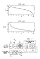
One phase delay compensation circuit may be implemented using the inverse of the low pass response of the Digital to Analog Converter (DAC). This DAC low pass function is generally implemented using a bank of switched capacitors for performing the digital to analog conversion and also for removing some of the high frequency images. The DAC low pass function may be a filter, for example, with a transfer function such as
where values for K, A and B can arbitrarily be chosen, for example, to emulate a real DAC operating at 2.048E6 Hz. In this case, K=1.1248, A=18.755 and B=17.63. The frequency and phase response associated with this DAC low pass filter are illustrated in FIG. 1. From the phase response shown in the lower plot, it can be seen there is a significant phase delay as indicated by the steep negative phase plot in the low frequency voice band; wherein the phase delay can be determined by looking at the phase divided by the frequency.
where values for K, A and B can arbitrarily be chosen, for example, to emulate a real DAC operating at 2.048E6 Hz. In this case, K=1.1248, A=18.755 and B=17.63. The frequency and phase response associated with this DAC low pass filter are illustrated in FIG. 1. From the phase response shown in the lower plot, it can be seen there is a significant phase delay as indicated by the steep negative phase plot in the low frequency voice band; wherein the phase delay can be determined by looking at the phase divided by the frequency.
Any DAC amplitude and phase changes can be fully corrected theoretically by applying the inverse of the DAC low pass function. In the case described above with reference to FIG. 1 , the inverse filter is a simple high pass Finite Impulse Response (FIR) filter defined as
The frequency and phase response of the high pass FIR filter defined by equation (2) are illustrated in FIG. 2. An examination of the plots depicted inFIGS. 1 and 2 reveals that the cascaded response of the two filters would be 1.
The frequency and phase response of the high pass FIR filter defined by equation (2) are illustrated in FIG. 2. An examination of the plots depicted in
The positive phase of the inverse filter provides some phase advancement (i.e. output predictive circuit) which predicts the next output value before it occurs. When this is combined with the exact negative phase of the DAC low pass filter, the result is a 0 phase response and a completely delay-corrected output signal. The present inventors have found that although this approach works in theory, the high gain of the inverse filter at higher frequencies can pose a problem for any high frequency noise components that exist in real systems, and that this is especially true for quantizer bit noise. A high frequency gain of over 30 dB, for example, will cause a real system to clip and compromise the Signal to Noise Ratio (SNR).
The present inventors found the foregoing problems could be solved by cascading the inverse filter with a simple low-order, low pass filter with a fairly wide bandwidth. This structure will then control the gain of the higher frequency bands by providing further attenuation for high frequency noise. This filter will however, add a small delay, but the inventors found that the small additional delay could be compensated for by adjusting the inverse filter response.
The present inventors also found that by varying the values of C and D, the high pass corner of the inverse filter could be scaled in the frequency domain. This will then scale the slope of the positive phase response of the inverse filter to provide the proper compensation for the extra delay of the cascaded low pass filter. The values can then be arbitrarily chosen to achieve any desired realizable magnitude and phase response. With continued reference to FIGS. 1 and 2 , and equations (1) and (2) discussed herein before, the inverse filter was simply the inverse of the DAC low pass filter, and was magnitude scaled to provide the desired phase response in order to match the DAC low pass filter. It can be seen from FIG. 2 however, that the phase slope of the inverse filter eventually becomes 0 and starts to become negative. This characteristic demonstrates that this filter scheme for delay correction is only good up to the frequency when the slope becomes negative (i.e. adds time delay), and that the predictive nature of the filter is limited up to that frequency. This filter scheme is perfectly fine as the phase slope transition frequency is well above about 4 kHz (closer to 100 kHz), and the slope in the voice band is almost linear regarding voice band codecs.
The present inventors also found the low pass filter 12 can be any desired low pass filter. One embodiment described herein below employed a 2nd order Chebyshev filter with a ripple of 0.1 dB and a corner frequency at 50 kHz. The combination of the 2nd order Chebyshev low pass filter and the inverse DAC filter 100 was found to provide the frequency response shown in FIG. 6.
Many other fixed processing delays exist in a digital impedance matching system which may also be corrected simply by adjusting the inverse DAC filter 100 coefficients to achieve the proper phase slope to correct for all of these static delays. These other static delays include the fixed Anti-Alias Filter (AAF) delay, Analog to Digital Converter (ADC) delays, digital impedance synthesis filter, and the image reject filter (IRF) on the output of the DAC low pass filter 12.
In summary explanation, a simple, power efficient and inexpensive digital compensation scheme is implemented for reducing delay in a digital impedance matching circuit to improve return loss. The scheme employs a digital filter to compensate for the absolute sampling and digital delays associated with a digital impedance matching circuit. The digital filter is based on the low-pass function of a DAC response, and can easily be modified to correct for not only the DAC response delay, but also other delays in the digital impedance matching circuit. The digital filter is very simple to implement and can add or subtract delays from the overall system.
Although the idea of phase and amplitude compensation is not new, the present invention described with reference to particular embodiments set forth herein before provides the first application of such concepts to improve digital impedance synthesis schemes. Known equalization schemes associated with other systems have been generally more concerned with phase equalization, where the phase response is modified to be linear over frequency, i.e. same delay. In contradistinction, the present invention implements phase correction circuits to actually reduce the overall signal delay.
In view of the above, it can be seen the present invention presents a significant advancement in the art of digital impedance matching circuits and systems. In view of the foregoing descriptions, it should be apparent that the present invention also represents a significant departure from the prior art in construction and operation. However, while particular embodiments of the present invention have been described herein in detail, it is to be understood that various alterations, modifications and substitutions can be made therein without departing in any way from the spirit and scope of the present invention, as defined in the claims which follow.
Claims (21)
1. A digital impedance matching circuit delay compensation system comprising:
a low-order low pass filter cascaded with an inverse DAC filter, wherein each filter is characterized by a respective transfer function having selectable coefficients such that the delay compensation system operates to reduce delays associated with a digital impedance matching circuit to improve return loss.
2. The delay compensation system according to claim 1 wherein the inverse DAC filter is an FIR filter.
3. The delay compensation system according to claim 1 wherein the inverse DAC filter is configured to provide a predicted output signal based on a previous input sample.
4. The delay compensation system according to claim 1 wherein the low-order low-pass filter is characterized by a transfer function defined by
5. The delay compensation system according to claim 1 wherein the inverse DAC filter is characterized by a transfer function defined by
6. The delay compensation system according to claim 1 wherein the inverse DAC filter is characterized by transfer function coefficients that are selectable to configure the inverse DAC filter to correct a plurality of static delays associated with an impedance matching circuit.
7. The delay compensation system according to claim 6 wherein the plurality of static delays are selected from the group consisting of a fixed anti-alias filter delay, an ADC delay, a digital impedance synthesis filter delay, a DAC delay, and an image reject filter delay.
8. The delay compensation system according to claim 1 wherein the low-pass filter is characterized by transfer function coefficients that are selectable to configure the low-pass filter to attenuate any high frequency noise such that large gains in the high frequency band of the inverse DAC filter will not cause signal clipping.
9. The delay compensation system according to claim 1 further comprising:
an anti-alias filter in communication with a tip/ring sense amplifier to generate an output signal;
an ADC operational to receive the anti-alias filter output signal and generate an ADC output signal;
a digital impedance synthesis filter operational to receive the ADC output signal and generate an input signal to the low-order low-pass filter;
a DAC operational to receive a signal generated by the inverse DAC filter;
a DAC low-pass filter operational to receive a signal generated by the DAC in response to the signal generated by the inverse DAC filter; and
an image reject filter operational to receive a signal generated by the DAC and generate an input signal to an analog impedance circuit.
10. The delay compensation system according to claim 1 wherein the low-order low-pass filter is a digital filter.
11. The delay compensation system according to claim 1 wherein the delay compensation system is devoid of purely analog devices.
12. A phase delay compensation system comprising:
filtering means for digitally passing a low frequency signal; and
an inverse DAC filter configured to process the filtered low frequency signal, wherein the delay compensation system is characterized by a plurality of transfer functions having selectable coefficients such that the delay compensation system operates to reduce static delays associated with a digital impedance matching circuit to improve return loss.
13. The phase delay compensation system according to claim 12 wherein the filtering means is a low-order, low-pass filter.
14. The delay compensation system according to claim 13 wherein the low-order low-pass filter is characterized by a transfer function defined by
15. The phase delay compensation system according to claim 12 wherein the inverse DAC filter is an FIR filter.
16. The phase delay compensation system according to claim 15 wherein the inverse DAC filter is characterized by a transfer function defined by
17. The phase delay compensation system according to claim 12 wherein the inverse DAC filter is configured to provide a predicted output signal based on a previous input sample.
18. The phase delay compensation system according to claim 12 wherein the inverse DAC filter is characterized by transfer function coefficients that are selected to configure the inverse DAC filter to correct a plurality of static delays associated with an impedance matching circuit.
19. The phase delay compensation system according to claim 18 wherein the plurality of static delays are selected from the group consisting of a fixed anti-alias filter delay, an ADC delay, a digital impedance synthesis filter delay, a DAC delay, and an image reject filter delay.
20. The phase delay compensation system according to claim 12 wherein the filtering means is characterized by transfer function coefficients that are selected to configure a low-order, low-pass filter to attenuate any high frequency noise such that large gains in the high frequency band associated with the inverse DAC filter will not cause signal clipping.
21. A method of compensating a digital impedance matching circuit to improve return loss comprising the steps of:
providing a phase delay compensation system having means for digitally filtering a low frequency signal and an inverse DAC filter configured to process the filtered low frequency signal;
placing the phase delay compensation system into a desired digital impedance matching circuit; and
setting transfer function coefficients associated with the digital filtering means and the inverse DAC filter such that the delay compensation system operates to reduce static delays associated with the digital impedance matching circuit to improve return loss.
Priority Applications (1)
| Application Number | Priority Date | Filing Date | Title |
|---|---|---|---|
| US10/123,677 US6920471B2 (en) | 2002-04-16 | 2002-04-16 | Compensation scheme for reducing delay in a digital impedance matching circuit to improve return loss |
Applications Claiming Priority (1)
| Application Number | Priority Date | Filing Date | Title |
|---|---|---|---|
| US10/123,677 US6920471B2 (en) | 2002-04-16 | 2002-04-16 | Compensation scheme for reducing delay in a digital impedance matching circuit to improve return loss |
Publications (2)
| Publication Number | Publication Date |
|---|---|
| US20030195909A1 US20030195909A1 (en) | 2003-10-16 |
| US6920471B2 true US6920471B2 (en) | 2005-07-19 |
Family
ID=28790784
Family Applications (1)
| Application Number | Title | Priority Date | Filing Date |
|---|---|---|---|
| US10/123,677 Expired - Lifetime US6920471B2 (en) | 2002-04-16 | 2002-04-16 | Compensation scheme for reducing delay in a digital impedance matching circuit to improve return loss |
Country Status (1)
| Country | Link |
|---|---|
| US (1) | US6920471B2 (en) |
Cited By (3)
| Publication number | Priority date | Publication date | Assignee | Title |
|---|---|---|---|---|
| US20060267677A1 (en) * | 2003-08-28 | 2006-11-30 | Koninklijke Philips Electronics N. V. | Method and system for passband ripple cancellation in cascading filters |
| US20070206775A1 (en) * | 2006-03-06 | 2007-09-06 | Winbond Electronics Corporation | Programmable plain old telephone line impedance matching circuits |
| US20090325632A1 (en) * | 2008-06-30 | 2009-12-31 | Simone Gambini | Loop delay compensation for continuous time sigma delta analog to digital converter |
Families Citing this family (2)
| Publication number | Priority date | Publication date | Assignee | Title |
|---|---|---|---|---|
| US9461660B2 (en) * | 2015-01-20 | 2016-10-04 | Mediatek Inc. | Digitally-corrected analog-to-digital converters |
| DE102021201202A1 (en) * | 2021-02-09 | 2022-08-11 | Carl Zeiss Smt Gmbh | Filter arrangement, in particular for a control loop for controlling the position of at least one element |
Citations (7)
| Publication number | Priority date | Publication date | Assignee | Title |
|---|---|---|---|---|
| US4677671A (en) * | 1982-11-26 | 1987-06-30 | International Business Machines Corp. | Method and device for coding a voice signal |
| US4720861A (en) * | 1985-12-24 | 1988-01-19 | Itt Defense Communications A Division Of Itt Corporation | Digital speech coding circuit |
| US4790015A (en) * | 1982-04-30 | 1988-12-06 | International Business Machines Corporation | Multirate digital transmission method and device for implementing said method |
| US4860317A (en) * | 1985-03-26 | 1989-08-22 | Devon County Council | Noise-reduction signal processing arrangement |
| US6047254A (en) * | 1996-05-15 | 2000-04-04 | Advanced Micro Devices, Inc. | System and method for determining a first formant analysis filter and prefiltering a speech signal for improved pitch estimation |
| US20030074192A1 (en) * | 2001-07-26 | 2003-04-17 | Hung-Bun Choi | Phase excited linear prediction encoder |
| US20040102967A1 (en) * | 2001-03-28 | 2004-05-27 | Satoru Furuta | Noise suppressor |
-
2002
- 2002-04-16 US US10/123,677 patent/US6920471B2/en not_active Expired - Lifetime
Patent Citations (7)
| Publication number | Priority date | Publication date | Assignee | Title |
|---|---|---|---|---|
| US4790015A (en) * | 1982-04-30 | 1988-12-06 | International Business Machines Corporation | Multirate digital transmission method and device for implementing said method |
| US4677671A (en) * | 1982-11-26 | 1987-06-30 | International Business Machines Corp. | Method and device for coding a voice signal |
| US4860317A (en) * | 1985-03-26 | 1989-08-22 | Devon County Council | Noise-reduction signal processing arrangement |
| US4720861A (en) * | 1985-12-24 | 1988-01-19 | Itt Defense Communications A Division Of Itt Corporation | Digital speech coding circuit |
| US6047254A (en) * | 1996-05-15 | 2000-04-04 | Advanced Micro Devices, Inc. | System and method for determining a first formant analysis filter and prefiltering a speech signal for improved pitch estimation |
| US20040102967A1 (en) * | 2001-03-28 | 2004-05-27 | Satoru Furuta | Noise suppressor |
| US20030074192A1 (en) * | 2001-07-26 | 2003-04-17 | Hung-Bun Choi | Phase excited linear prediction encoder |
Cited By (5)
| Publication number | Priority date | Publication date | Assignee | Title |
|---|---|---|---|---|
| US20060267677A1 (en) * | 2003-08-28 | 2006-11-30 | Koninklijke Philips Electronics N. V. | Method and system for passband ripple cancellation in cascading filters |
| US20070206775A1 (en) * | 2006-03-06 | 2007-09-06 | Winbond Electronics Corporation | Programmable plain old telephone line impedance matching circuits |
| US7957522B2 (en) | 2006-03-06 | 2011-06-07 | Winbond Electronics Corporation | Programmable plain old telephone line impedance matching circuits |
| US20090325632A1 (en) * | 2008-06-30 | 2009-12-31 | Simone Gambini | Loop delay compensation for continuous time sigma delta analog to digital converter |
| US8195221B2 (en) * | 2008-06-30 | 2012-06-05 | Intel Corporation | Loop delay compensation for continuous time sigma delta analog to digital converter |
Also Published As
| Publication number | Publication date |
|---|---|
| US20030195909A1 (en) | 2003-10-16 |
Similar Documents
| Publication | Publication Date | Title |
|---|---|---|
| US6570514B1 (en) | Linearity error compensator | |
| US20060083297A1 (en) | Filters for communication systems | |
| US5633863A (en) | Echo canceler | |
| US5263191A (en) | Method and circuit for processing and filtering signals | |
| JP3122793B2 (en) | Method and nonlinear filter for reducing co-channel interference | |
| US8660820B2 (en) | Distortion cancellation using adaptive linearization | |
| JP2985675B2 (en) | Method and apparatus for identifying unknown system by band division adaptive filter | |
| KR20050121606A (en) | Digital sampling rate converter for compensating signal droop in band | |
| US7688235B2 (en) | Composite analog to digital receiver with adaptive self-linearization | |
| US4882547A (en) | Linearizer control system | |
| US7693672B2 (en) | Adaptive self-linearization | |
| AU767997B2 (en) | Arrangement and method for interference cancelling | |
| US5825826A (en) | Method and apparatus for frequency domain ripple compensation for a communications transmitter | |
| US6920471B2 (en) | Compensation scheme for reducing delay in a digital impedance matching circuit to improve return loss | |
| CN110808750B (en) | Method and device for suppressing adjacent channel interference based on inverse filtering | |
| US5428834A (en) | Method and circuit for processing and filtering signals | |
| CN109327768B (en) | Active noise reduction system | |
| US8379740B2 (en) | Wide-band signal processor | |
| JP3902498B2 (en) | Image signal suppressor | |
| Barcellos et al. | Design of FIR filters combining the frequency-response masking and the WLS-Chebyshev approaches | |
| US20030130751A1 (en) | New filter bank for graphics equalizer implementation | |
| JPH0557767B2 (en) | ||
| Lim et al. | Digital compensation in IQ modulators using adaptive FIR filters | |
| JP2006505211A (en) | Multistage nonlinear echo canceller for digital communication systems with or without frequency division duplexing. | |
| US6507300B1 (en) | Variable rate decimator |
Legal Events
| Date | Code | Title | Description |
|---|---|---|---|
| AS | Assignment |
Owner name: TEXAS INSTRUMENTS INCORPORATED, TEXAS Free format text: ASSIGNMENT OF ASSIGNORS INTEREST;ASSIGNORS:CHAN, WING K.;NABICHT, JOSEPH T.;REEL/FRAME:012834/0985 Effective date: 20020405 |
|
| STCF | Information on status: patent grant |
Free format text: PATENTED CASE |
|
| FPAY | Fee payment |
Year of fee payment: 4 |
|
| FPAY | Fee payment |
Year of fee payment: 8 |
|
| FPAY | Fee payment |
Year of fee payment: 12 |