US6829666B1 - Modular computing architecture having common communication interface - Google Patents
Modular computing architecture having common communication interface Download PDFInfo
- Publication number
- US6829666B1 US6829666B1 US09/408,874 US40887499A US6829666B1 US 6829666 B1 US6829666 B1 US 6829666B1 US 40887499 A US40887499 A US 40887499A US 6829666 B1 US6829666 B1 US 6829666B1
- Authority
- US
- United States
- Prior art keywords
- communication interface
- common communication
- node
- interface
- level
- Prior art date
- Legal status (The legal status is an assumption and is not a legal conclusion. Google has not performed a legal analysis and makes no representation as to the accuracy of the status listed.)
- Expired - Lifetime
Links
Images


Classifications
-
- G—PHYSICS
- G06—COMPUTING; CALCULATING OR COUNTING
- G06F—ELECTRIC DIGITAL DATA PROCESSING
- G06F15/00—Digital computers in general; Data processing equipment in general
- G06F15/16—Combinations of two or more digital computers each having at least an arithmetic unit, a program unit and a register, e.g. for a simultaneous processing of several programs
- G06F15/163—Interprocessor communication
- G06F15/173—Interprocessor communication using an interconnection network, e.g. matrix, shuffle, pyramid, star, snowflake
- G06F15/17337—Direct connection machines, e.g. completely connected computers, point to point communication networks
- G06F15/17343—Direct connection machines, e.g. completely connected computers, point to point communication networks wherein the interconnection is dynamically configurable, e.g. having loosely coupled nearest neighbor architecture
-
- G—PHYSICS
- G06—COMPUTING; CALCULATING OR COUNTING
- G06F—ELECTRIC DIGITAL DATA PROCESSING
- G06F15/00—Digital computers in general; Data processing equipment in general
- G06F15/16—Combinations of two or more digital computers each having at least an arithmetic unit, a program unit and a register, e.g. for a simultaneous processing of several programs
- G06F15/163—Interprocessor communication
- G06F15/173—Interprocessor communication using an interconnection network, e.g. matrix, shuffle, pyramid, star, snowflake
- G06F15/17356—Indirect interconnection networks
- G06F15/17368—Indirect interconnection networks non hierarchical topologies
- G06F15/17381—Two dimensional, e.g. mesh, torus
Definitions
- This invention is generally related to the field of high-speed computing systems and, more particularly, to a computer architecture having an flexible and incrementally scalable common communication interface that facilitates a wide variety of modular computing topologies.
- the present invention is directed to a distributed, shared memory computer architecture that is organized into a number of nodes, where each node has at least one processor.
- each node includes a common communication interface that facilitates the ability to incrementally build and swap the nodes of the system without disrupting the overall computing resources of the system. More specifically, the common communication interface within each node connects local memory to the local processors, provides a port for communicating with a system-wide routing network and a port for communicating with an I/O subsystem.
- each computing topology is a superset of smaller topologies supported by the architecture. As such, computing systems based upon the architecture may be easily and incrementally scaled without reconfiguring the existing components.
- FIGS. 1A and 1B are logical block diagrams that illustrate various embodiments of how the functionally independent modules of the inventive architecture may be combined in various topologies to form a high-speed computing systems.
- FIG. 1C illustrates three high-speed computing systems constructed using the flexible and scalable modular system described herein.
- FIG. 1D illustrates a high-performance processing system 140 having six vertical racks suitable for the modules described herein.
- FIG. 2A illustrates one embodiment of a C-Brick. This module contains four CPUs and eight memory slots.
- FIG. 3 illustrates an isometric view of a router module 300 herein referred to as the R-Brick.
- FIG. 4 illustrates an isometric view of an I/O module referred to herein as an X-Brick.
- FIG. 5 is an isometric view of an input/output module 500 herein referred to as an I-Brick.
- FIG. 6 illustrates one embodiment of an output module 600 referred to herein as a P-Brick, which is a more powerful input/output module than the I-Brick 500 .
- FIG. 7 illustrates a computer rack 700 suitable for receiving one or more independent modules as described in this application.
- FIG. 8 is an isometric view illustrating a power module 800 herein referred to as a P-Bay.
- FIG. 9 illustrates a wiring diagram for a typical high-speed computing system comprising the flexible and scalable independently functional modules described herein.
- FIGS. 10, 11 and 12 illustrate possible topologies based on the above discussed interconnect rules.
- FIG. 13 illustrates one embodiment of a common communication interface present within each node of the architecture, thereby facilitating their flexible and scalable interconnection.
- FIG. 14 illustrates one embodiment of an internal message format used by the common communication interface of FIG. 13 .
- FIG. 15 is a block diagram illustrating one embodiment of an internal, high-speed crossbar of the common communication interface.
- the present invention is directed to a distributed, shared memory computer architecture that is organized into a number of nodes, where each node has at least one processor.
- each node includes a common communication interface that facilitates the ability to incrementally build and swap the nodes of the system without disrupting the overall computing resources of the system. More specifically, the common communication interface within each node connects local memory to the local processors, provides a port for communicating with a system-wide routing network and a port for communicating with an I/O subsystem.
- independent routing modules are used within the architecture to communicatively couple the nodes in a wide variety of topologies.
- highly flexible and scalable high-speed computers may easily be constructed.
- the computer architecture is especially useful in constructing computing systems having a large number of processors, such as up to 4096, that share a single address space and require cache coherence across all of the nodes of the high-speed computer.
- processing nodes and the routing modules are the basic building blocks for configuring a high-speed computing system and, therefore, are collectively referred to as bricks that may readily be interconnected in a variety of topologies.
- the computing system may include an arbitrary combination of processing nodes and other modules such that there need not be a fixed relation between the number of processing nodes and the other modules.
- each topology supported by the architecture is a superset of the smaller topologies supported by the architecture. Table 1 illustrates the various modules used within the computer architecture.
- C-Brick-MIPS A CPU node populated with the MIPS processors.
- C-Brick-Merced A CPU brick populated Merced processors.
- R-Brick A routing node providing eight routing ports.
- Power Bay A power bay providing power to a given rack of modules.
- D-Brick A diskette or disc drive module also referred to as a disc box.
- FIGS. 1A and 1B are logical block diagrams that illustrate various embodiments of how the functionally independent bricks described above may be combined in various topologies to form high-speed computing systems.
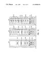
- FIG. 1A illustrates three computer topologies 10 , 15 and 20 .
- Topology 10 illustrates a single node having four processors (P) connected by a single common communication interface (BR).
- Topology 20 illustrates an eight processor topology in which two nodes are communicatively coupled via their respective common communication interfaces.
- Topology 30 illustrates a sixteen processor topology in which four nodes are communicatively coupled via a single routing module.
- FIG. 1B illustrates an extended hypercube computer topology in which nodes having 512 processors are interconnected according to the flexible architecture described herein.
- each computing topology is a superset of smaller topologies supported by the architecture. More specifically, topology 15 is a superset that includes two topologies 10 . Similarly, topology 20 is a superset that includes four topologies 10 , or two topologies 15 . As such, computing systems based upon the inventive architecture described herein may be easily and incrementally scaled without reconfiguring the existing components.
- FIG. 1C illustrates an isometric view of three high-speed, rack-mounted computing systems constructed using functionally independent bricks and architecture of the present invention. More specifically, high-speed computing system 100 illustrates a low-cost entry into high-speed computing and includes power bay modules (Pwr Bay) 102 , two processing nodes (C-Bricks) 104 that include multiple processors, a single routing module (R-Brick) 106 and a single input/output module (I-Brick) 108 .
- Pwr Bay power bay modules
- C-Bricks processing nodes
- R-Brick routing module
- I-Brick input/output module
- High-speed computing system 120 illustrates an intermediate system with two processing nodes (C-Brick 124 ), a single routing module (R-Brick) 126 , a single I/O module (I-Brick) 128 , two power modules (Pwr Bay) 122 and three drive bays (D-Bricks) 129 .
- High-speed computing system 130 illustrates a higher end computer having power modules (Pwr Bay) 132 and network connection module 133 , four processing nodes (C-Bricks) 134 and routing module (R-Brick) 136 .
- the four remaining I/O modules can be any combination of P-Bricks, I-Bricks and X-Bricks.
- FIG. 1D illustrates one quarter of a high-performance processing system 140 .
- Six vertical racks of the twenty-four are illustrated.
- computing system 140 can have up to eight C-Bricks per rack, up to 16 racks for a total of 512 CPUs.
- system 140 can have two or three routing modules per rack and multiple power bays per rack.
- Computing system 140 further includes multiple I/O racks 142 that may comprise one to eight P, I or X Bricks.
- FIG. 2 illustrates one embodiment of a processing node 200 of the present invention.
- the processing node 200 referred to as a C-Brick, is a functionally independent module containing four local CPUs, local memory and the associated electronics required to operate as an independent distributed module.
- a C-Brick provides the following: 1) a high-speed serial channel to communicate between a system controller and the brick, 2) a high-speed serial channel to communicate with an internal level one (L1) system controller, 3) an external high-speed serial console port for a serial channel to communicate with an L1 system controller in an I/O-Brick.
- the illustrated embodiment contains four CPUs 215 and eight memory slots 222 .
- Memory slots 222 are designed to accept DIMM modules which support two rows of ten SDRAM chips.
- Front-mounted fans 228 are removable from the front, redundant and hot-swappable.
- External connectors 230 at the rear of the C-Brick 200 provide connections for power, routing network, I/O, and Universal Serial Bus (USB). As described below, the USB connector is used for connection to an optional level two (L2) system controller in small systems that do not have a routing module.
- L2 level two
- Processing node 200 includes a common communications interface 235 that facilitates the ability to incrementally build and swap the nodes of the system without disrupting the overall computing resources of the system. More specifically, the common communications interface 235 within node 200 connects local memory present in slots 222 to local processors 215 and, as discussed in detail below, provides a intelligent, high-speed interface to connectors 230 .
- FIG. 3 is a block diagram illustrating a routing module 300 herein referred to as an R-Brick.
- the R-Brick provides the following: 1) a high-speed serial channel to communicate between an internal L1 system controller and an internal router ASIC, 2) a USB slave port to communicate with a level two (L2) system controller and a level three (L3) system controller, 3) a USB hub with five master ports.
- R-Brick 300 contains a single router ASIC 310 , power circuitry 312 , interface connectors 320 and 322 , a level two (L2) system controller 315 , USB hub 325 and USP upstream connector 327 .
- Connectors 320 and 322 are D-Net connectors that, according to the invention, allow various modules to easily be interconnected and interchanged.
- Four of the D-Net connectors 320 of R-Brick 300 carry L2 system controller USB signaling.
- Another four D-Net connectors 322 carry all router-to-router communications.
- four C-Bricks may be coupled to R-Brick 300 via connectors 320 while four other routing modules may be connected to R-Brick 300 via connectors 322 .
- router module 300 has only six ports.
- I/O modules are provided by the inventive computer architecture: an I-Brick, an X-Brick and a P-Brick.
- the I-Brick is intended to provide all of the IO needs for a basic system or to provide the boot requirements of a larger, more complex system.
- the P-brick provides twelve 64 bit PCI slots.
- the X-Brick is an IO expansion brick that provides four half-height XIO slots.
- FIG. 4 illustrates an isometric view of an I/O module referred to herein as an X-Brick.
- the X-Brick provides the following functionality: 1) a serial channel to communicate with an internal L1 system controller within a C-Brick, and 2) a means for reading and reporting the population of the I/O cards. More specifically, X-Brick 400 includes four I/O cards 404 that plug horizontally from the rear of box 402 . A single host interface card also plugs horizontally from the rear. A mid-plane PCA 410 mounted vertically in the center of X-Brick 400 contains a single X-Bridge ASIC 412 for controlling I/O.
- FIG. 5 is an isometric view of an input/output module 500 herein referred to as an I-Brick.
- the I-Brick and the P-Brick provides the following: 1) a serial channel to communicate with the internal L1 controller within a C-Brick, 2) a means for reading and reporting the population of PCI cards, 3) a means for controlling the powering of PCI slots, 4) a means for controlling and monitoring the status of the power bay.
- I-Brick 500 includes six PCI input/output boards 512 and a CDROM/DVD player 510 .
- Power board 522 houses a single X-Bridge ASIC for controlling I/O.
- a pair of XTalk I/O ports are located on the rear of I/O module 500 and connect I-Brick 500 to one or two C-Bricks.
- I-Brick 500 contains two removable fiber channel hard drives and a single removable media drive 510 .
- Power board 522 mounts horizontally from the front of I-Brick 500 and accepts 48 volts DC as input and generates the required DC voltages for the system board, the PCI slots 512 , disc drives 510 .
- FIG. 6 illustrates one embodiment of an output module 600 referred to herein as a P-Brick, which is a more powerful input/output module than the I-Brick 500 . More specifically, P-Brick 600 houses three X-Bridge ASICs and provides 12 PCI slots 602 .
- FIG. 7 is an isometric view of a computer rack 700 suitable for receiving one or more independent modules as described in this application.
- rack 700 can receive one or more C-Bricks, P-Bricks, I-Bricks or X-Bricks. In this manner, a scalable computer may easily be manufactured.
- Other embodiments of rack 700 are possible, such as a short rack or a dual-column rack.
- FIG. 8 is an isometric view illustrating a power module 800 herein referred to as a Pwr-Bay.
- Pwr-Bay 800 holds up to six power supplies that are single-phase AC input and 950 watts at 48 VDC output each.
- Pwr-Bay 800 includes eight connectors 804 on the rear of the module. These connectors carry the 48 VDC power along with monitoring signals.
- P-Bay 804 further includes eight serial interfaces for monitoring each power supply.
- the distributed architecture described herein requires, in one embodiment, a 48 volt supply.
- the distributed architecture of the present invention has a three-level hierarchy for system management.
- the heart of the architecture is an L1 system controller (not illustrated) that exists within each brick of the inventive architecture except the D-brick.
- This controller includes a microcontroller, a system monitoring chip, a scan interface chip, plus a collection of serial EPROMs, bus expanders and communication interfaces which are specific to the device it controls.
- the L1 system controller is responsible for power control and sequencing, environmental control and monitoring, initiation of reset, and the storage of identification and configuration information for its host brick.
- the L1 system controller also provides console/diagnostic and scanned interfaces to the user.
- FIG. 9 illustrates a wiring diagram for a typical high-speed computing system comprising the functional modules described herein.
- An L2 system controller 904 provides rack-level system control, i.e., there is one L2 system controller 904 for each rack having C-Bricks. Moreover, the L2 system controller 904 acts as a central communications clearinghouse for the rack and controls all of the bricks in that particular rack and associated I/O racks.
- each L2 system controller 904 is equipped with a touch screen display and ethernet and modem ports, and can be used as a central point of control for the system.
- a third level of control is the L3 system controller 906 that provides a central point of control for the entire system and, in one embodiment, is a standalone workstation or laptop.
- Computing system 900 includes a first rack 902 that contains two routing modules 910 (R-Bricks) and eight processing nodes 914 (C-Bricks). Because each routing modules 910 has four ports, four C-Bricks may be coupled to the router. Each C-Brick 914 is connected to one of the routing modules 910 via a single high-speed USB cable. Similarly, each routing module 914 is connected to the L2 system controller 904 via USB cables. Computing system 900 further includes a meta-router 912 .
- the first CPU rack 902 also includes a single ethernet hub 914 that connects to additional CPU racks via local network 920 . In addition, the L3 system controller may connect to other computers via network 925 .
- the L1 system controller within each brick provides direct low-level communications and control for all of the functions within a brick. In most systems, it acts as a slave to upstream L2 system controller 904 . In one embodiment, however, which are limited to a smaller number of processing modules C-Bricks, one L1 system controller may act as a master controller for the entire system if no L2 system controller 904 is present.
- an L3 system controller may communicate directly to the L1 system controller of a C-Brick. Because a C-Brick has a standard upstream USB port, it is possible for the L3 to interface directly to the system without an L2. If there is an L2, then the upstream USB port of the C-Brick will be made inaccessible because the L1 of the C-Brick will already be using that USB channel to communicate with an R-Brick L1. It is also possible for an L3 system controller to communicate directly to an L2 system controller. As discussed above, this is typically via a network connection through a network hub. Otherwise, an L3 system controller can be connected directly to an L2 with a cross over twisted pair cable. If a routing module is included in the computing system, a L2 system controller is required.
- the L2 system controller will act as a USB host for the particular rack.
- the L1 controller of the routing module contains a USB hub which drives the USB signaling to the local L1 and out on the four ports which are connected to the C-Bricks. It is therefore possible for an R-Brick to be coupled directly to a C-Brick.
- An R-Brick has a USB hub whose downstream ports will be routed in a shielded pair to the L1 system controller of the C-Brick.
- the L1 system controller of the bricks communicate with each other via RS422 over cables.
- the L1 system controller of a C-Brick it is possible for the L1 system controller of a C-Brick to be coupled directly to the L1 system controller of an I/O-Brick. Since the C-Bricks and I/O-Bricks need to communicate in routerless systems, they are configured to communicate via RS422 over cables as well.
- FIGS. 10, 11 and 12 illustrate possible topologies based on the above discussed possible interconnections.
- Interconnections 1005 illustrate computing systems that do not have a routing module and therefore C-Bricks are connected directly to I-Bricks. As illustrated, these interconnects use a serial 422 connection over a standard cable.
- Topologies 1010 illustrate computing systems having an L3 system controller and no L2 system controller. Here the L3 system controller uses a USB connection directly to the C-Bricks.
- interconnections 1115 illustrate computing systems having three or more C-Bricks which, therefore, require a routing module, in which case an L2 system host is required.
- the L2 system controller is a USB host and the routing modules are USB hubs.
- interconnection topology 1208 illustrates a computing system having multiple L2 system controllers connected via a 10-base T hub.
- an L3 system controller is optionally connected to the 10-base T hub.
- FIG. 13 illustrates one embodiment of an inventive high-speed common communication interface 1300 for interconnecting the various independent modules described herein.
- common communication interface 1300 provides connectivity between the various modules in a fair and efficient manner.
- Each node within the computing system includes a common communication interface 1300 that, as discussed in detail below, extends a “virtual” system bus throughout the distributed modules of the high-speed computing system. In this manner, processing nodes and other modules may be easily added and removed from the computing system.
- Common communication interface 1300 includes four distinct interfaces.
- a A processor interface 1305 interfaces to one or more processing modules.
- Memory interface 1310 for interfacing to a portion of the global memory and for maintaining cache coherency across the computing system.
- I/O interface 1315 for communicating with an I/O subsystem.
- Common communication interface 1300 further includes a router interface 1320 for interfacing to a router module.
- common communication interface 1300 includes five interface control units for managing its interfaces. More specifically, common communication interface 1300 includes a processor interface unit 1325 , a memory interface unit 1330 , an I/O interface unit 1335 , a network interface unit 1340 , and a local block 1345 for interfacing with the local chip resources. In this manner, common communication interface 1300 provides standard connectivity between four types of external interfaces and an interface to local chip resources.
- common communication interface 1300 facilitates distributed modular computing systems that share a single address space.
- common communication interface 1300 supports up to 256 processing nodes which, in one embodiment, comprise up to four processors each.
- Each interface control unit within common communication interface 1300 communicates by forwarding messages through, and receiving sending messages from, crossbar 1350 .
- the messages used by the modules conform to a packetized network protocol.
- two types of messages are supported: requests and replies. This configuration helps the computing system avoid system deadlock situations and promotes cache coherence.
- I/O interface 1335 or network interface 1330 the message is converted to an internal format. The reverse occurs when a message is sent via one of these interfaces.
- the internal message format for common communication interface 1300 consists of a header frame that is a group of bits that is conceptually and logically a single unit. This header frame is optionally followed by one or more data frames carrying a total of 64-1,024 bits of data for the message. As each frame is received by or transmitted from common communication interface 1300 . Control signals embedded within the frame indicate all or some of the following information: 1) to which interface control unit the frame is destined, 2) whether the frame is a request or reply, and 3) whether the frame concludes the current message.
- FIG. 14 illustrates one embodiment of an internal message format for common communication interface 1300 . More specifically, FIG. 14 illustrates control bits, header format and data formats. Within the header, a source is indicated via the most significant 11 bits. In one embodiment, the source identifies a device and a node.
- Crossbar 1350 of common communication interface 1300 supports the flow of messages in the internal format discussed above along two virtual channels, multiplexed across physical channels connecting each unit of common communication interface 1300 to crossbar 1350 .
- Crossbar 1350 is designed for minimal latency under light loads by means of a buffer queue bypass paths and maximum throughput under heavy loads by means of per virtual channel arbitration requests. It is in this manner that a plurality of nodes 135 may by used to interconnect the computing modules discussed herein in a variety of topologies.
- FIG. 15 is a block diagram of one embodiment of crossbar 1350 of common communication interface 1300 .
- a dual-FIFO refers to two virtual channel FIFOs within a single buffer memory structure.
- a quad-FIFO refers to four virtual channels in an analogous structure.
- Data path crossbar 1505 contains an 8-input by 6-output crossbar.
- the crossbar data path is 67 bits wide for all inputs and outputs and provides a 1.6 GB/s of data bandwidth per port at a 5 NS clock.
- the output queues provide buffering for outgoing unit messages and arbitrate for data path resources.
- the input queues provide buffering for data that has traversed the crossbar 1350 but has not yet been processed by its destination unit. Their primary role, therefore, is to provide rate matching and synchronization between crossbar 1350 and the receiving unit.
- Arbiter 1510 provides low-latency arbitration for uncontested ports via bypass arbitration and efficient high utilization via wave front arbitration as resources become saturated.
Abstract
Description
| TABLE 1 | |
| Brick | Description |
| C-Brick-MIPS | A CPU node populated with the MIPS processors. |
| C-Brick-Merced | A CPU brick populated Merced processors. |
| P-Brick | An IO brick that provides 14 PCI slots. |
| I-Brick | An I/O brick that supports complete IO needs |
| of an entry level system. | |
| X-Brick | An IO brick that provides four XIO slots. |
| R-Brick | A routing node providing eight routing ports. |
| Power Bay | A power bay providing power to a given rack |
| of modules. | |
| D-Brick | A diskette or disc drive module also referred |
| to as a disc box. | |
Claims (25)
Priority Applications (4)
| Application Number | Priority Date | Filing Date | Title |
|---|---|---|---|
| US09/408,874 US6829666B1 (en) | 1999-09-29 | 1999-09-29 | Modular computing architecture having common communication interface |
| EP00967100A EP1222550A2 (en) | 1999-09-29 | 2000-09-29 | Modular computing architecture having common communication interface |
| PCT/US2000/026824 WO2001024017A2 (en) | 1999-09-29 | 2000-09-29 | Modular computing architecture having common communication interface |
| JP2001526717A JP2003510719A (en) | 1999-09-29 | 2000-09-29 | Modular computing architecture with common communication interface |
Applications Claiming Priority (1)
| Application Number | Priority Date | Filing Date | Title |
|---|---|---|---|
| US09/408,874 US6829666B1 (en) | 1999-09-29 | 1999-09-29 | Modular computing architecture having common communication interface |
Publications (1)
| Publication Number | Publication Date |
|---|---|
| US6829666B1 true US6829666B1 (en) | 2004-12-07 |
Family
ID=23618133
Family Applications (1)
| Application Number | Title | Priority Date | Filing Date |
|---|---|---|---|
| US09/408,874 Expired - Lifetime US6829666B1 (en) | 1999-09-29 | 1999-09-29 | Modular computing architecture having common communication interface |
Country Status (4)
| Country | Link |
|---|---|
| US (1) | US6829666B1 (en) |
| EP (1) | EP1222550A2 (en) |
| JP (1) | JP2003510719A (en) |
| WO (1) | WO2001024017A2 (en) |
Cited By (14)
| Publication number | Priority date | Publication date | Assignee | Title |
|---|---|---|---|---|
| US20020080775A1 (en) * | 2000-11-22 | 2002-06-27 | International Business Machines Corporation | Switching nodes and interface modules for data networks |
| US20050071843A1 (en) * | 2001-12-20 | 2005-03-31 | Hong Guo | Topology aware scheduling for a multiprocessor system |
| US20090198918A1 (en) * | 2008-02-01 | 2009-08-06 | Arimilli Lakshminarayana B | Host Fabric Interface (HFI) to Perform Global Shared Memory (GSM) Operations |
| US20090199209A1 (en) * | 2008-02-01 | 2009-08-06 | Arimilli Lakshminarayana B | Mechanism for Guaranteeing Delivery of Multi-Packet GSM Message |
| US20090199182A1 (en) * | 2008-02-01 | 2009-08-06 | Arimilli Lakshminarayana B | Notification by Task of Completion of GSM Operations at Target Node |
| US20090199200A1 (en) * | 2008-02-01 | 2009-08-06 | Arimilli Lakshminarayana B | Mechanisms to Order Global Shared Memory Operations |
| US20090199195A1 (en) * | 2008-02-01 | 2009-08-06 | Arimilli Lakshminarayana B | Generating and Issuing Global Shared Memory Operations Via a Send FIFO |
| US20090199194A1 (en) * | 2008-02-01 | 2009-08-06 | Arimilli Lakshminarayana B | Mechanism to Prevent Illegal Access to Task Address Space by Unauthorized Tasks |
| US20090199191A1 (en) * | 2008-02-01 | 2009-08-06 | Arimilli Lakshminarayana B | Notification to Task of Completion of GSM Operations by Initiator Node |
| US20100008038A1 (en) * | 2008-05-15 | 2010-01-14 | Giovanni Coglitore | Apparatus and Method for Reliable and Efficient Computing Based on Separating Computing Modules From Components With Moving Parts |
| US20130184840A1 (en) * | 2012-01-12 | 2013-07-18 | Rockwell Automation Asia Pacific Business Center Pte. Ltd. | System and method for coupling an automation controller and scaleable module |
| US20160139880A1 (en) * | 2014-11-14 | 2016-05-19 | Cavium, Inc. | Bypass FIFO for Multiple Virtual Channels |
| US20190303326A1 (en) * | 2018-03-30 | 2019-10-03 | Provino Technologies, Inc. | Arbitrating portions of transactions over virtual channels associated with an interconnect |
| US11340671B2 (en) | 2018-03-30 | 2022-05-24 | Google Llc | Protocol level control for system on a chip (SOC) agent reset and power management |
Families Citing this family (1)
| Publication number | Priority date | Publication date | Assignee | Title |
|---|---|---|---|---|
| US6829697B1 (en) * | 2000-09-06 | 2004-12-07 | International Business Machines Corporation | Multiple logical interfaces to a shared coprocessor resource |
Citations (8)
| Publication number | Priority date | Publication date | Assignee | Title |
|---|---|---|---|---|
| US5339396A (en) * | 1987-11-18 | 1994-08-16 | Hitachi, Ltd. | Interconnection network and crossbar switch for the same |
| US5504874A (en) | 1993-09-29 | 1996-04-02 | Silicon Graphics, Inc. | System and method of implementing read resources to maintain cache coherency in a multiprocessor environment permitting split transactions |
| US5509125A (en) | 1993-09-29 | 1996-04-16 | Silicon Graphics, Inc. | System and method for fair arbitration on a multi-domain multiprocessor bus |
| US5682479A (en) * | 1995-05-05 | 1997-10-28 | Silicon Graphics, Inc. | System and method for network exploration and access |
| US5721819A (en) * | 1995-05-05 | 1998-02-24 | Silicon Graphics Corporation | Programmable, distributed network routing |
| US5878241A (en) | 1990-11-13 | 1999-03-02 | International Business Machine | Partitioning of processing elements in a SIMD/MIMD array processor |
| WO1999026429A2 (en) | 1997-11-17 | 1999-05-27 | Cray Research, Inc. | Hybrid hypercube/torus architecture |
| US6055599A (en) * | 1995-09-11 | 2000-04-25 | Electronics & Telecommunications Research Institute | Hierarchical crossbar interconnection network for a cluster-based parallel processing computer |
-
1999
- 1999-09-29 US US09/408,874 patent/US6829666B1/en not_active Expired - Lifetime
-
2000
- 2000-09-29 WO PCT/US2000/026824 patent/WO2001024017A2/en active Application Filing
- 2000-09-29 JP JP2001526717A patent/JP2003510719A/en active Pending
- 2000-09-29 EP EP00967100A patent/EP1222550A2/en not_active Withdrawn
Patent Citations (9)
| Publication number | Priority date | Publication date | Assignee | Title |
|---|---|---|---|---|
| US5339396A (en) * | 1987-11-18 | 1994-08-16 | Hitachi, Ltd. | Interconnection network and crossbar switch for the same |
| US5878241A (en) | 1990-11-13 | 1999-03-02 | International Business Machine | Partitioning of processing elements in a SIMD/MIMD array processor |
| US5504874A (en) | 1993-09-29 | 1996-04-02 | Silicon Graphics, Inc. | System and method of implementing read resources to maintain cache coherency in a multiprocessor environment permitting split transactions |
| US5509125A (en) | 1993-09-29 | 1996-04-16 | Silicon Graphics, Inc. | System and method for fair arbitration on a multi-domain multiprocessor bus |
| US5664151A (en) | 1993-09-29 | 1997-09-02 | Silicon Graphics, Inc. | System and method of implementing read resources to maintain cache coherency in a multiprocessor environment permitting split transactions |
| US5682479A (en) * | 1995-05-05 | 1997-10-28 | Silicon Graphics, Inc. | System and method for network exploration and access |
| US5721819A (en) * | 1995-05-05 | 1998-02-24 | Silicon Graphics Corporation | Programmable, distributed network routing |
| US6055599A (en) * | 1995-09-11 | 2000-04-25 | Electronics & Telecommunications Research Institute | Hierarchical crossbar interconnection network for a cluster-based parallel processing computer |
| WO1999026429A2 (en) | 1997-11-17 | 1999-05-27 | Cray Research, Inc. | Hybrid hypercube/torus architecture |
Non-Patent Citations (1)
| Title |
|---|
| Laudon, J., et al., "The SGI Origin: A ccNUMA Highly Scalable Server", Computer ARchitecture News, vol. 25, No. 2, XP000656582, 241-251, (May 1997). |
Cited By (30)
| Publication number | Priority date | Publication date | Assignee | Title |
|---|---|---|---|---|
| US20020080775A1 (en) * | 2000-11-22 | 2002-06-27 | International Business Machines Corporation | Switching nodes and interface modules for data networks |
| US6996116B2 (en) * | 2000-11-22 | 2006-02-07 | International Business Machines Corporation | Switching nodes and interface modules for data networks |
| US20050071843A1 (en) * | 2001-12-20 | 2005-03-31 | Hong Guo | Topology aware scheduling for a multiprocessor system |
| US8239879B2 (en) | 2008-02-01 | 2012-08-07 | International Business Machines Corporation | Notification by task of completion of GSM operations at target node |
| US8484307B2 (en) | 2008-02-01 | 2013-07-09 | International Business Machines Corporation | Host fabric interface (HFI) to perform global shared memory (GSM) operations |
| US20090199182A1 (en) * | 2008-02-01 | 2009-08-06 | Arimilli Lakshminarayana B | Notification by Task of Completion of GSM Operations at Target Node |
| US20090199200A1 (en) * | 2008-02-01 | 2009-08-06 | Arimilli Lakshminarayana B | Mechanisms to Order Global Shared Memory Operations |
| US20090199195A1 (en) * | 2008-02-01 | 2009-08-06 | Arimilli Lakshminarayana B | Generating and Issuing Global Shared Memory Operations Via a Send FIFO |
| US20090199194A1 (en) * | 2008-02-01 | 2009-08-06 | Arimilli Lakshminarayana B | Mechanism to Prevent Illegal Access to Task Address Space by Unauthorized Tasks |
| US20090199191A1 (en) * | 2008-02-01 | 2009-08-06 | Arimilli Lakshminarayana B | Notification to Task of Completion of GSM Operations by Initiator Node |
| US20090199209A1 (en) * | 2008-02-01 | 2009-08-06 | Arimilli Lakshminarayana B | Mechanism for Guaranteeing Delivery of Multi-Packet GSM Message |
| US8146094B2 (en) | 2008-02-01 | 2012-03-27 | International Business Machines Corporation | Guaranteeing delivery of multi-packet GSM messages |
| US8200910B2 (en) | 2008-02-01 | 2012-06-12 | International Business Machines Corporation | Generating and issuing global shared memory operations via a send FIFO |
| US8214604B2 (en) | 2008-02-01 | 2012-07-03 | International Business Machines Corporation | Mechanisms to order global shared memory operations |
| US20090198918A1 (en) * | 2008-02-01 | 2009-08-06 | Arimilli Lakshminarayana B | Host Fabric Interface (HFI) to Perform Global Shared Memory (GSM) Operations |
| US8255913B2 (en) | 2008-02-01 | 2012-08-28 | International Business Machines Corporation | Notification to task of completion of GSM operations by initiator node |
| US8275947B2 (en) | 2008-02-01 | 2012-09-25 | International Business Machines Corporation | Mechanism to prevent illegal access to task address space by unauthorized tasks |
| US20100008038A1 (en) * | 2008-05-15 | 2010-01-14 | Giovanni Coglitore | Apparatus and Method for Reliable and Efficient Computing Based on Separating Computing Modules From Components With Moving Parts |
| US20130184840A1 (en) * | 2012-01-12 | 2013-07-18 | Rockwell Automation Asia Pacific Business Center Pte. Ltd. | System and method for coupling an automation controller and scaleable module |
| US9459595B2 (en) * | 2012-01-12 | 2016-10-04 | Rockwell Automation Asia Pacific Business Center Pte. Ltd. | System and method for coupling an automation controller and scaleable module |
| US20160139880A1 (en) * | 2014-11-14 | 2016-05-19 | Cavium, Inc. | Bypass FIFO for Multiple Virtual Channels |
| US9824058B2 (en) * | 2014-11-14 | 2017-11-21 | Cavium, Inc. | Bypass FIFO for multiple virtual channels |
| US20190303326A1 (en) * | 2018-03-30 | 2019-10-03 | Provino Technologies, Inc. | Arbitrating portions of transactions over virtual channels associated with an interconnect |
| US20190303325A1 (en) * | 2018-03-30 | 2019-10-03 | Provino Technologies, Inc. | Arbitrating portions of transactions over virtual channels associated with an interconnect |
| US10838891B2 (en) * | 2018-03-30 | 2020-11-17 | Provino Technologies, Inc. | Arbitrating portions of transactions over virtual channels associated with an interconnect |
| US10853282B2 (en) * | 2018-03-30 | 2020-12-01 | Provino Technologies, Inc. | Arbitrating portions of transactions over virtual channels associated with an interconnect |
| US11003604B2 (en) | 2018-03-30 | 2021-05-11 | Provino Technologies, Inc. | Procedures for improving efficiency of an interconnect fabric on a system on chip |
| US11340671B2 (en) | 2018-03-30 | 2022-05-24 | Google Llc | Protocol level control for system on a chip (SOC) agent reset and power management |
| US11640362B2 (en) | 2018-03-30 | 2023-05-02 | Google Llc | Procedures for improving efficiency of an interconnect fabric on a system on chip |
| US11914440B2 (en) | 2018-03-30 | 2024-02-27 | Google Llc | Protocol level control for system on a chip (SoC) agent reset and power management |
Also Published As
| Publication number | Publication date |
|---|---|
| EP1222550A2 (en) | 2002-07-17 |
| WO2001024017A3 (en) | 2001-08-16 |
| JP2003510719A (en) | 2003-03-18 |
| WO2001024017A2 (en) | 2001-04-05 |
Similar Documents
| Publication | Publication Date | Title |
|---|---|---|
| US6829666B1 (en) | Modular computing architecture having common communication interface | |
| US8116332B2 (en) | Switch arbitration | |
| US7533210B2 (en) | Virtual communication interfaces for a micro-controller | |
| US9965442B2 (en) | Node card management in a modular and large scalable server system | |
| US6633946B1 (en) | Flexible switch-based I/O system interconnect | |
| JPH0713945A (en) | Bus structure of multiprocessor system with separated arithmetic processing part and control/storage part | |
| US20120170492A1 (en) | Serial memory and io access architecture and system for switched telecommunication and computing platforms | |
| CN100484003C (en) | Server | |
| CN100445981C (en) | Computer system using serial connect bus, and method for interconnecting a plurality of CPU using serial connect bus | |
| EP2230606A2 (en) | System having a plurality of nodes connected in multi-dimensional matrix, method of controlling system and apparatus | |
| US5533201A (en) | Method and apparatus for simultaneous interconnection of multiple requestors to multiple memories | |
| WO2006058288A2 (en) | Disaggregated star platform management bus architecture system | |
| CN213338710U (en) | Heterogeneous computing server based on full connection of multiple FPGA board cards | |
| CN1901530B (en) | Server system | |
| US20060294317A1 (en) | Symmetric multiprocessor architecture with interchangeable processor and IO modules | |
| CN112347033A (en) | Multi-unit server implementation method based on VPX architecture | |
| US6701387B1 (en) | Adaptive data fetch prediction algorithm | |
| CN216352292U (en) | Server mainboard and server | |
| US20050038949A1 (en) | Apparatus for enabling distributed processing across a plurality of circuit cards | |
| US20070226456A1 (en) | System and method for employing multiple processors in a computer system | |
| US20060129709A1 (en) | Multipurpose scalable server communication link | |
| Gustavson | Introduction to the Fastbus | |
| US6804737B2 (en) | Methods and systems for intelligent I/O controller with channel expandability via master/slave configuration | |
| US20070101169A1 (en) | IC with dual communication interfaces | |
| Kwon et al. | Microserver architecture with high-speed interconnected network |
Legal Events
| Date | Code | Title | Description |
|---|---|---|---|
| AS | Assignment |
Owner name: SILICON GRAPHICS, INC., CALIFORNIA Free format text: ASSIGNMENT OF ASSIGNORS INTEREST;ASSIGNORS:DENEROFF, MARTIN M.;DEAN, STEVE;MCCANN, TIMOTHY S.;AND OTHERS;REEL/FRAME:010482/0899;SIGNING DATES FROM 19991123 TO 19991221 |
|
| STCF | Information on status: patent grant |
Free format text: PATENTED CASE |
|
| CC | Certificate of correction | ||
| AS | Assignment |
Owner name: WELLS FARGO FOOTHILL CAPITAL, INC.,CALIFORNIA Free format text: SECURITY AGREEMENT;ASSIGNOR:SILICON GRAPHICS, INC. AND SILICON GRAPHICS FEDERAL, INC. (EACH A DELAWARE CORPORATION);REEL/FRAME:016871/0809 Effective date: 20050412 Owner name: WELLS FARGO FOOTHILL CAPITAL, INC., CALIFORNIA Free format text: SECURITY AGREEMENT;ASSIGNOR:SILICON GRAPHICS, INC. AND SILICON GRAPHICS FEDERAL, INC. (EACH A DELAWARE CORPORATION);REEL/FRAME:016871/0809 Effective date: 20050412 |
|
| AS | Assignment |
Owner name: GENERAL ELECTRIC CAPITAL CORPORATION,CALIFORNIA Free format text: SECURITY INTEREST;ASSIGNOR:SILICON GRAPHICS, INC.;REEL/FRAME:018545/0777 Effective date: 20061017 Owner name: GENERAL ELECTRIC CAPITAL CORPORATION, CALIFORNIA Free format text: SECURITY INTEREST;ASSIGNOR:SILICON GRAPHICS, INC.;REEL/FRAME:018545/0777 Effective date: 20061017 |
|
| AS | Assignment |
Owner name: MORGAN STANLEY & CO., INCORPORATED, NEW YORK Free format text: ASSIGNMENT OF ASSIGNORS INTEREST;ASSIGNOR:GENERAL ELECTRIC CAPITAL CORPORATION;REEL/FRAME:019995/0895 Effective date: 20070926 Owner name: MORGAN STANLEY & CO., INCORPORATED,NEW YORK Free format text: ASSIGNMENT OF ASSIGNORS INTEREST;ASSIGNOR:GENERAL ELECTRIC CAPITAL CORPORATION;REEL/FRAME:019995/0895 Effective date: 20070926 |
|
| FPAY | Fee payment |
Year of fee payment: 4 |
|
| REMI | Maintenance fee reminder mailed | ||
| AS | Assignment |
Owner name: SILICON GRAPHICS INTERNATIONAL, CORP., CALIFORNIA Free format text: ASSIGNMENT OF ASSIGNORS INTEREST;ASSIGNORS:SILICON GRAPHICS, INC. ET AL.;SGI INTERNATIONAL, INC.;SIGNING DATES FROM 20090508 TO 20120208;REEL/FRAME:027727/0020 |
|
| FPAY | Fee payment |
Year of fee payment: 8 |
|
| AS | Assignment |
Owner name: SILICON GRAPHICS INTERNATIONAL CORP., CALIFORNIA Free format text: MERGER;ASSIGNOR:SGI INTERNATIONAL, INC.;REEL/FRAME:034804/0437 Effective date: 20120808 Owner name: SGI INTERNATIONAL, INC., CALIFORNIA Free format text: CHANGE OF NAME;ASSIGNOR:SILICON GRAPHICS INTERNATIONAL, INC.;REEL/FRAME:034804/0661 Effective date: 20090513 Owner name: SILICON GRAPHICS INTERNATIONAL, INC., CALIFORNIA Free format text: ASSIGNMENT OF ASSIGNORS INTEREST;ASSIGNOR:SILICON GRAPHICS, INC.;REEL/FRAME:034804/0446 Effective date: 20090508 |
|
| AS | Assignment |
Owner name: MORGAN STANLEY SENIOR FUNDING, INC., NEW YORK Free format text: SECURITY INTEREST;ASSIGNOR:SILICON GRAPHICS INTERNATIONAL CORP.;REEL/FRAME:035200/0722 Effective date: 20150127 |
|
| FPAY | Fee payment |
Year of fee payment: 12 |
|
| AS | Assignment |
Owner name: SILICON GRAPHICS, INC., CALIFORNIA Free format text: ORDER. . . AUTHORIZING THE SALE OF ALL OR SUBSTANTIALLY ALL OF THE ASSETS OF THE DEBTORS FREE AND CLEAR OF ALL LIENS, CLAIMS, ENCUMBRANCES, AND INTERESTS;ASSIGNOR:MORGAN STANLEY &CO., INCORPORATED;REEL/FRAME:039636/0812 Effective date: 20090508 Owner name: SILICON GRAPHICS, INC., CALIFORNIA Free format text: ORDER. . . AUTHORIZING THE SALE OF ALL OR SUBSTANTIALLY ALL OF THE ASSETS OF THE DEBTORS FREE AND CLEAR OF ALL LIENS, CLAIMS, ENCUMBRANCES, AND INTERESTS;ASSIGNOR:WELLS FARGO FOOTHILL CAPITAL, INC.;REEL/FRAME:039645/0914 Effective date: 20090430 |
|
| AS | Assignment |
Owner name: SILICON GRAPHICS INTERNATIONAL CORP., CALIFORNIA Free format text: RELEASE BY SECURED PARTY;ASSIGNOR:MORGAN STANLEY SENIOR FUNDING, INC., AS AGENT;REEL/FRAME:040545/0362 Effective date: 20161101 |
|
| AS | Assignment |
Owner name: HEWLETT PACKARD ENTERPRISE DEVELOPMENT LP, TEXAS Free format text: ASSIGNMENT OF ASSIGNORS INTEREST;ASSIGNOR:SILICON GRAPHICS INTERNATIONAL CORP.;REEL/FRAME:044128/0149 Effective date: 20170501 |