US6806491B2 - Organic light-emitting devices - Google Patents
Organic light-emitting devices Download PDFInfo
- Publication number
- US6806491B2 US6806491B2 US10/351,070 US35107003A US6806491B2 US 6806491 B2 US6806491 B2 US 6806491B2 US 35107003 A US35107003 A US 35107003A US 6806491 B2 US6806491 B2 US 6806491B2
- Authority
- US
- United States
- Prior art keywords
- layer
- organic
- npb
- organic material
- emitting device
- Prior art date
- Legal status (The legal status is an assumption and is not a legal conclusion. Google has not performed a legal analysis and makes no representation as to the accuracy of the status listed.)
- Expired - Lifetime
Links
- 239000011368 organic material Substances 0.000 claims abstract description 62
- 239000000758 substrate Substances 0.000 claims abstract description 54
- TVIVIEFSHFOWTE-UHFFFAOYSA-K tri(quinolin-8-yloxy)alumane Chemical compound [Al+3].C1=CN=C2C([O-])=CC=CC2=C1.C1=CN=C2C([O-])=CC=CC2=C1.C1=CN=C2C([O-])=CC=CC2=C1 TVIVIEFSHFOWTE-UHFFFAOYSA-K 0.000 claims description 74
- YYMBJDOZVAITBP-UHFFFAOYSA-N rubrene Chemical compound C1=CC=CC=C1C(C1=C(C=2C=CC=CC=2)C2=CC=CC=C2C(C=2C=CC=CC=2)=C11)=C(C=CC=C2)C2=C1C1=CC=CC=C1 YYMBJDOZVAITBP-UHFFFAOYSA-N 0.000 claims description 70
- 239000000463 material Substances 0.000 claims description 39
- 239000000872 buffer Substances 0.000 claims description 20
- -1 polyphenylene Polymers 0.000 claims description 11
- IEQIEDJGQAUEQZ-UHFFFAOYSA-N phthalocyanine Chemical group N1C(N=C2C3=CC=CC=C3C(N=C3C4=CC=CC=C4C(=N4)N3)=N2)=C(C=CC=C2)C2=C1N=C1C2=CC=CC=C2C4=N1 IEQIEDJGQAUEQZ-UHFFFAOYSA-N 0.000 claims description 8
- MSDMPJCOOXURQD-UHFFFAOYSA-N C545T Chemical compound C1=CC=C2SC(C3=CC=4C=C5C6=C(C=4OC3=O)C(C)(C)CCN6CCC5(C)C)=NC2=C1 MSDMPJCOOXURQD-UHFFFAOYSA-N 0.000 claims description 6
- HFACYLZERDEVSX-UHFFFAOYSA-N benzidine Chemical class C1=CC(N)=CC=C1C1=CC=C(N)C=C1 HFACYLZERDEVSX-UHFFFAOYSA-N 0.000 claims description 5
- IBHBKWKFFTZAHE-UHFFFAOYSA-N n-[4-[4-(n-naphthalen-1-ylanilino)phenyl]phenyl]-n-phenylnaphthalen-1-amine Chemical compound C1=CC=CC=C1N(C=1C2=CC=CC=C2C=CC=1)C1=CC=C(C=2C=CC(=CC=2)N(C=2C=CC=CC=2)C=2C3=CC=CC=C3C=CC=2)C=C1 IBHBKWKFFTZAHE-UHFFFAOYSA-N 0.000 claims description 5
- 150000004866 oxadiazoles Chemical class 0.000 claims description 5
- 229910052751 metal Inorganic materials 0.000 claims description 4
- 239000002184 metal Substances 0.000 claims description 4
- VVOPUZNLRVJDJQ-UHFFFAOYSA-N phthalocyanine copper Chemical compound [Cu].C12=CC=CC=C2C(N=C2NC(C3=CC=CC=C32)=N2)=NC1=NC([C]1C=CC=CC1=1)=NC=1N=C1[C]3C=CC=CC3=C2N1 VVOPUZNLRVJDJQ-UHFFFAOYSA-N 0.000 claims description 4
- 229920003227 poly(N-vinyl carbazole) Polymers 0.000 claims description 4
- 150000003233 pyrroles Chemical class 0.000 claims description 4
- 229920000265 Polyparaphenylene Polymers 0.000 claims description 3
- 229910052782 aluminium Inorganic materials 0.000 claims description 3
- 150000004697 chelate complex Chemical class 0.000 claims description 3
- 150000001893 coumarin derivatives Chemical class 0.000 claims description 3
- YLYPIBBGWLKELC-RMKNXTFCSA-N 2-[2-[(e)-2-[4-(dimethylamino)phenyl]ethenyl]-6-methylpyran-4-ylidene]propanedinitrile Chemical compound C1=CC(N(C)C)=CC=C1\C=C\C1=CC(=C(C#N)C#N)C=C(C)O1 YLYPIBBGWLKELC-RMKNXTFCSA-N 0.000 claims description 2
- OGGKVJMNFFSDEV-UHFFFAOYSA-N 3-methyl-n-[4-[4-(n-(3-methylphenyl)anilino)phenyl]phenyl]-n-phenylaniline Chemical compound CC1=CC=CC(N(C=2C=CC=CC=2)C=2C=CC(=CC=2)C=2C=CC(=CC=2)N(C=2C=CC=CC=2)C=2C=C(C)C=CC=2)=C1 OGGKVJMNFFSDEV-UHFFFAOYSA-N 0.000 claims description 2
- GYHNNYVSQQEPJS-UHFFFAOYSA-N Gallium Chemical compound [Ga] GYHNNYVSQQEPJS-UHFFFAOYSA-N 0.000 claims description 2
- GWAGJZBUMGWMLH-UHFFFAOYSA-N acridin-4-ol;zinc Chemical compound [Zn].C1=CC=C2N=C3C(O)=CC=CC3=CC2=C1 GWAGJZBUMGWMLH-UHFFFAOYSA-N 0.000 claims description 2
- XAGFODPZIPBFFR-UHFFFAOYSA-N aluminium Chemical compound [Al] XAGFODPZIPBFFR-UHFFFAOYSA-N 0.000 claims description 2
- XZCJVWCMJYNSQO-UHFFFAOYSA-N butyl pbd Chemical compound C1=CC(C(C)(C)C)=CC=C1C1=NN=C(C=2C=CC(=CC=2)C=2C=CC=CC=2)O1 XZCJVWCMJYNSQO-UHFFFAOYSA-N 0.000 claims description 2
- 229910052733 gallium Inorganic materials 0.000 claims description 2
- WCPAKWJPBJAGKN-UHFFFAOYSA-N oxadiazole Chemical compound C1=CON=N1 WCPAKWJPBJAGKN-UHFFFAOYSA-N 0.000 claims description 2
- 229910052720 vanadium Inorganic materials 0.000 claims description 2
- LEONUFNNVUYDNQ-UHFFFAOYSA-N vanadium atom Chemical compound [V] LEONUFNNVUYDNQ-UHFFFAOYSA-N 0.000 claims description 2
- 238000004776 molecular orbital Methods 0.000 claims 4
- 150000001716 carbazoles Chemical class 0.000 claims 3
- SCBQASHPRZSHFA-UHFFFAOYSA-N 2,9-dimethyl-4,7-diphenyl-1,10-phenanthroline;4,7-diphenyl-1,10-phenanthroline Chemical compound C1=CC=CC=C1C1=CC=NC2=C1C=CC1=C(C=3C=CC=CC=3)C=CN=C21.C=12C=CC3=C(C=4C=CC=CC=4)C=C(C)N=C3C2=NC(C)=CC=1C1=CC=CC=C1 SCBQASHPRZSHFA-UHFFFAOYSA-N 0.000 claims 1
- GEQBRULPNIVQPP-UHFFFAOYSA-N 2-[3,5-bis(1-phenylbenzimidazol-2-yl)phenyl]-1-phenylbenzimidazole Chemical compound C1=CC=CC=C1N1C2=CC=CC=C2N=C1C1=CC(C=2N(C3=CC=CC=C3N=2)C=2C=CC=CC=2)=CC(C=2N(C3=CC=CC=C3N=2)C=2C=CC=CC=2)=C1 GEQBRULPNIVQPP-UHFFFAOYSA-N 0.000 claims 1
- SLIUAWYAILUBJU-UHFFFAOYSA-N pentacene Chemical compound C1=CC=CC2=CC3=CC4=CC5=CC=CC=C5C=C4C=C3C=C21 SLIUAWYAILUBJU-UHFFFAOYSA-N 0.000 claims 1
- 238000004770 highest occupied molecular orbital Methods 0.000 abstract description 6
- 238000004768 lowest unoccupied molecular orbital Methods 0.000 abstract description 6
- 239000010410 layer Substances 0.000 description 367
- 239000010408 film Substances 0.000 description 113
- 230000008021 deposition Effects 0.000 description 89
- XCJYREBRNVKWGJ-UHFFFAOYSA-N copper(II) phthalocyanine Chemical compound [Cu+2].C12=CC=CC=C2C(N=C2[N-]C(C3=CC=CC=C32)=N2)=NC1=NC([C]1C=CC=CC1=1)=NC=1N=C1[C]3C=CC=CC3=C2[N-]1 XCJYREBRNVKWGJ-UHFFFAOYSA-N 0.000 description 63
- 239000011521 glass Substances 0.000 description 44
- XLYOFNOQVPJJNP-UHFFFAOYSA-N water Substances O XLYOFNOQVPJJNP-UHFFFAOYSA-N 0.000 description 24
- 229910001316 Ag alloy Inorganic materials 0.000 description 15
- 229910045601 alloy Inorganic materials 0.000 description 13
- 239000000956 alloy Substances 0.000 description 13
- 238000009835 boiling Methods 0.000 description 12
- 239000000969 carrier Substances 0.000 description 12
- 229910001092 metal group alloy Inorganic materials 0.000 description 12
- JEGUKCSWCFPDGT-UHFFFAOYSA-N h2o hydrate Chemical compound O.O JEGUKCSWCFPDGT-UHFFFAOYSA-N 0.000 description 11
- 230000004888 barrier function Effects 0.000 description 9
- 238000000034 method Methods 0.000 description 9
- 238000001194 electroluminescence spectrum Methods 0.000 description 6
- HXWWMGJBPGRWRS-CMDGGOBGSA-N 4- -2-tert-butyl-6- -4h-pyran Chemical compound O1C(C(C)(C)C)=CC(=C(C#N)C#N)C=C1\C=C\C1=CC(C(CCN2CCC3(C)C)(C)C)=C2C3=C1 HXWWMGJBPGRWRS-CMDGGOBGSA-N 0.000 description 5
- 230000000052 comparative effect Effects 0.000 description 5
- 239000011701 zinc Substances 0.000 description 5
- 238000002347 injection Methods 0.000 description 4
- 239000007924 injection Substances 0.000 description 4
- 229920001609 Poly(3,4-ethylenedioxythiophene) Polymers 0.000 description 3
- 239000004642 Polyimide Substances 0.000 description 3
- 229920000767 polyaniline Polymers 0.000 description 3
- 229920001721 polyimide Polymers 0.000 description 3
- 238000005215 recombination Methods 0.000 description 3
- 230000006798 recombination Effects 0.000 description 3
- RYGMFSIKBFXOCR-UHFFFAOYSA-N Copper Chemical compound [Cu] RYGMFSIKBFXOCR-UHFFFAOYSA-N 0.000 description 2
- XLOMVQKBTHCTTD-UHFFFAOYSA-N Zinc monoxide Chemical compound [Zn]=O XLOMVQKBTHCTTD-UHFFFAOYSA-N 0.000 description 2
- 230000015572 biosynthetic process Effects 0.000 description 2
- 125000000609 carbazolyl group Chemical class C1(=CC=CC=2C3=CC=CC=C3NC12)* 0.000 description 2
- 229910052802 copper Inorganic materials 0.000 description 2
- 239000010949 copper Substances 0.000 description 2
- PCHJSUWPFVWCPO-UHFFFAOYSA-N gold Chemical compound [Au] PCHJSUWPFVWCPO-UHFFFAOYSA-N 0.000 description 2
- 229910052737 gold Inorganic materials 0.000 description 2
- 239000010931 gold Substances 0.000 description 2
- AMGQUBHHOARCQH-UHFFFAOYSA-N indium;oxotin Chemical compound [In].[Sn]=O AMGQUBHHOARCQH-UHFFFAOYSA-N 0.000 description 2
- 238000004519 manufacturing process Methods 0.000 description 2
- YRZZLAGRKZIJJI-UHFFFAOYSA-N oxyvanadium phthalocyanine Chemical compound [V+2]=O.C12=CC=CC=C2C(N=C2[N-]C(C3=CC=CC=C32)=N2)=NC1=NC([C]1C=CC=CC1=1)=NC=1N=C1[C]3C=CC=CC3=C2[N-]1 YRZZLAGRKZIJJI-UHFFFAOYSA-N 0.000 description 2
- IKXKTLBKRBLWNN-UHFFFAOYSA-N pentacene Chemical compound C1=CC=CC2=CC3=CC4=CC5=CC=CC=C5C=C4C=C3C=C21.C1=CC=CC2=CC3=CC4=CC5=CC=CC=C5C=C4C=C3C=C21 IKXKTLBKRBLWNN-UHFFFAOYSA-N 0.000 description 2
- 229920000139 polyethylene terephthalate Polymers 0.000 description 2
- 239000005020 polyethylene terephthalate Substances 0.000 description 2
- 229920000642 polymer Polymers 0.000 description 2
- 238000001228 spectrum Methods 0.000 description 2
- 239000010409 thin film Substances 0.000 description 2
- XNCMQRWVMWLODV-UHFFFAOYSA-N 1-phenylbenzimidazole Chemical compound C1=NC2=CC=CC=C2N1C1=CC=CC=C1 XNCMQRWVMWLODV-UHFFFAOYSA-N 0.000 description 1
- STTGYIUESPWXOW-UHFFFAOYSA-N 2,9-dimethyl-4,7-diphenyl-1,10-phenanthroline Chemical compound C=12C=CC3=C(C=4C=CC=CC=4)C=C(C)N=C3C2=NC(C)=CC=1C1=CC=CC=C1 STTGYIUESPWXOW-UHFFFAOYSA-N 0.000 description 1
- VZSRBBMJRBPUNF-UHFFFAOYSA-N 2-(2,3-dihydro-1H-inden-2-ylamino)-N-[3-oxo-3-(2,4,6,7-tetrahydrotriazolo[4,5-c]pyridin-5-yl)propyl]pyrimidine-5-carboxamide Chemical compound C1C(CC2=CC=CC=C12)NC1=NC=C(C=N1)C(=O)NCCC(N1CC2=C(CC1)NN=N2)=O VZSRBBMJRBPUNF-UHFFFAOYSA-N 0.000 description 1
- DHDHJYNTEFLIHY-UHFFFAOYSA-N 4,7-diphenyl-1,10-phenanthroline Chemical compound C1=CC=CC=C1C1=CC=NC2=C1C=CC1=C(C=3C=CC=CC=3)C=CN=C21 DHDHJYNTEFLIHY-UHFFFAOYSA-N 0.000 description 1
- 108091006149 Electron carriers Proteins 0.000 description 1
- YCKRFDGAMUMZLT-UHFFFAOYSA-N Fluorine atom Chemical compound [F] YCKRFDGAMUMZLT-UHFFFAOYSA-N 0.000 description 1
- BQCADISMDOOEFD-UHFFFAOYSA-N Silver Chemical compound [Ag] BQCADISMDOOEFD-UHFFFAOYSA-N 0.000 description 1
- 230000004075 alteration Effects 0.000 description 1
- 239000003086 colorant Substances 0.000 description 1
- 239000002322 conducting polymer Substances 0.000 description 1
- 229920001940 conductive polymer Polymers 0.000 description 1
- 230000003247 decreasing effect Effects 0.000 description 1
- 229910003460 diamond Inorganic materials 0.000 description 1
- 239000010432 diamond Substances 0.000 description 1
- 239000002019 doping agent Substances 0.000 description 1
- 238000000295 emission spectrum Methods 0.000 description 1
- 230000002708 enhancing effect Effects 0.000 description 1
- 229910052731 fluorine Inorganic materials 0.000 description 1
- 239000011737 fluorine Substances 0.000 description 1
- 229920002313 fluoropolymer Polymers 0.000 description 1
- 239000004811 fluoropolymer Substances 0.000 description 1
- 230000005525 hole transport Effects 0.000 description 1
- 230000005524 hole trap Effects 0.000 description 1
- 229910052738 indium Inorganic materials 0.000 description 1
- 229910010272 inorganic material Inorganic materials 0.000 description 1
- 239000011147 inorganic material Substances 0.000 description 1
- 229910052809 inorganic oxide Inorganic materials 0.000 description 1
- 239000002346 layers by function Substances 0.000 description 1
- 239000007769 metal material Substances 0.000 description 1
- 229910044991 metal oxide Inorganic materials 0.000 description 1
- 150000004706 metal oxides Chemical class 0.000 description 1
- 150000002739 metals Chemical class 0.000 description 1
- 229920000620 organic polymer Polymers 0.000 description 1
- KYKLWYKWCAYAJY-UHFFFAOYSA-N oxotin;zinc Chemical compound [Zn].[Sn]=O KYKLWYKWCAYAJY-UHFFFAOYSA-N 0.000 description 1
- 239000002861 polymer material Substances 0.000 description 1
- 150000003839 salts Chemical class 0.000 description 1
- 229910052709 silver Inorganic materials 0.000 description 1
- 239000004332 silver Substances 0.000 description 1
- 239000007787 solid Substances 0.000 description 1
- 239000000243 solution Substances 0.000 description 1
- 230000003595 spectral effect Effects 0.000 description 1
- 230000005641 tunneling Effects 0.000 description 1
- 238000007740 vapor deposition Methods 0.000 description 1
- 239000011787 zinc oxide Substances 0.000 description 1
Images


Classifications
-
- H—ELECTRICITY
- H10—SEMICONDUCTOR DEVICES; ELECTRIC SOLID-STATE DEVICES NOT OTHERWISE PROVIDED FOR
- H10K—ORGANIC ELECTRIC SOLID-STATE DEVICES
- H10K50/00—Organic light-emitting devices
- H10K50/10—OLEDs or polymer light-emitting diodes [PLED]
- H10K50/14—Carrier transporting layers
-
- H—ELECTRICITY
- H10—SEMICONDUCTOR DEVICES; ELECTRIC SOLID-STATE DEVICES NOT OTHERWISE PROVIDED FOR
- H10K—ORGANIC ELECTRIC SOLID-STATE DEVICES
- H10K50/00—Organic light-emitting devices
- H10K50/10—OLEDs or polymer light-emitting diodes [PLED]
- H10K50/14—Carrier transporting layers
- H10K50/15—Hole transporting layers
-
- H—ELECTRICITY
- H10—SEMICONDUCTOR DEVICES; ELECTRIC SOLID-STATE DEVICES NOT OTHERWISE PROVIDED FOR
- H10K—ORGANIC ELECTRIC SOLID-STATE DEVICES
- H10K50/00—Organic light-emitting devices
- H10K50/10—OLEDs or polymer light-emitting diodes [PLED]
- H10K50/17—Carrier injection layers
-
- H—ELECTRICITY
- H10—SEMICONDUCTOR DEVICES; ELECTRIC SOLID-STATE DEVICES NOT OTHERWISE PROVIDED FOR
- H10K—ORGANIC ELECTRIC SOLID-STATE DEVICES
- H10K85/00—Organic materials used in the body or electrodes of devices covered by this subclass
- H10K85/10—Organic polymers or oligomers
- H10K85/111—Organic polymers or oligomers comprising aromatic, heteroaromatic, or aryl chains, e.g. polyaniline, polyphenylene or polyphenylene vinylene
- H10K85/113—Heteroaromatic compounds comprising sulfur or selene, e.g. polythiophene
- H10K85/1135—Polyethylene dioxythiophene [PEDOT]; Derivatives thereof
-
- H—ELECTRICITY
- H10—SEMICONDUCTOR DEVICES; ELECTRIC SOLID-STATE DEVICES NOT OTHERWISE PROVIDED FOR
- H10K—ORGANIC ELECTRIC SOLID-STATE DEVICES
- H10K85/00—Organic materials used in the body or electrodes of devices covered by this subclass
- H10K85/10—Organic polymers or oligomers
- H10K85/141—Organic polymers or oligomers comprising aliphatic or olefinic chains, e.g. poly N-vinylcarbazol, PVC or PTFE
- H10K85/146—Organic polymers or oligomers comprising aliphatic or olefinic chains, e.g. poly N-vinylcarbazol, PVC or PTFE poly N-vinylcarbazol; Derivatives thereof
-
- H—ELECTRICITY
- H10—SEMICONDUCTOR DEVICES; ELECTRIC SOLID-STATE DEVICES NOT OTHERWISE PROVIDED FOR
- H10K—ORGANIC ELECTRIC SOLID-STATE DEVICES
- H10K85/00—Organic materials used in the body or electrodes of devices covered by this subclass
- H10K85/30—Coordination compounds
-
- H—ELECTRICITY
- H10—SEMICONDUCTOR DEVICES; ELECTRIC SOLID-STATE DEVICES NOT OTHERWISE PROVIDED FOR
- H10K—ORGANIC ELECTRIC SOLID-STATE DEVICES
- H10K85/00—Organic materials used in the body or electrodes of devices covered by this subclass
- H10K85/30—Coordination compounds
- H10K85/311—Phthalocyanine
-
- H—ELECTRICITY
- H10—SEMICONDUCTOR DEVICES; ELECTRIC SOLID-STATE DEVICES NOT OTHERWISE PROVIDED FOR
- H10K—ORGANIC ELECTRIC SOLID-STATE DEVICES
- H10K85/00—Organic materials used in the body or electrodes of devices covered by this subclass
- H10K85/30—Coordination compounds
- H10K85/321—Metal complexes comprising a group IIIA element, e.g. Tris (8-hydroxyquinoline) gallium [Gaq3]
- H10K85/324—Metal complexes comprising a group IIIA element, e.g. Tris (8-hydroxyquinoline) gallium [Gaq3] comprising aluminium, e.g. Alq3
-
- H—ELECTRICITY
- H10—SEMICONDUCTOR DEVICES; ELECTRIC SOLID-STATE DEVICES NOT OTHERWISE PROVIDED FOR
- H10K—ORGANIC ELECTRIC SOLID-STATE DEVICES
- H10K85/00—Organic materials used in the body or electrodes of devices covered by this subclass
- H10K85/60—Organic compounds having low molecular weight
- H10K85/615—Polycyclic condensed aromatic hydrocarbons, e.g. anthracene
-
- H—ELECTRICITY
- H10—SEMICONDUCTOR DEVICES; ELECTRIC SOLID-STATE DEVICES NOT OTHERWISE PROVIDED FOR
- H10K—ORGANIC ELECTRIC SOLID-STATE DEVICES
- H10K85/00—Organic materials used in the body or electrodes of devices covered by this subclass
- H10K85/60—Organic compounds having low molecular weight
- H10K85/631—Amine compounds having at least two aryl rest on at least one amine-nitrogen atom, e.g. triphenylamine
-
- H—ELECTRICITY
- H10—SEMICONDUCTOR DEVICES; ELECTRIC SOLID-STATE DEVICES NOT OTHERWISE PROVIDED FOR
- H10K—ORGANIC ELECTRIC SOLID-STATE DEVICES
- H10K85/00—Organic materials used in the body or electrodes of devices covered by this subclass
- H10K85/60—Organic compounds having low molecular weight
- H10K85/649—Aromatic compounds comprising a hetero atom
- H10K85/656—Aromatic compounds comprising a hetero atom comprising two or more different heteroatoms per ring
- H10K85/6565—Oxadiazole compounds
-
- Y—GENERAL TAGGING OF NEW TECHNOLOGICAL DEVELOPMENTS; GENERAL TAGGING OF CROSS-SECTIONAL TECHNOLOGIES SPANNING OVER SEVERAL SECTIONS OF THE IPC; TECHNICAL SUBJECTS COVERED BY FORMER USPC CROSS-REFERENCE ART COLLECTIONS [XRACs] AND DIGESTS
- Y10—TECHNICAL SUBJECTS COVERED BY FORMER USPC
- Y10S—TECHNICAL SUBJECTS COVERED BY FORMER USPC CROSS-REFERENCE ART COLLECTIONS [XRACs] AND DIGESTS
- Y10S977/00—Nanotechnology
- Y10S977/902—Specified use of nanostructure
- Y10S977/932—Specified use of nanostructure for electronic or optoelectronic application
- Y10S977/949—Radiation emitter using nanostructure
- Y10S977/95—Electromagnetic energy
Definitions
- the present invention relates to organic light-emitting devices. More particularly, this invention provides highly luminance-efficient and bright organic light-emitting devices, and organic light-emitting devices with adjustable emission zone.
- OLEDs organic light-emitting devices
- advantages such as self-emission, low voltage operation, all-solid state, wide view angle, and full-color.
- the OLEDs also show a quick responding speed of up to 1000 times that of the LCD display and its manufacturing cost is relatively low comparing with the LCD display with same distinguishability.
- OLEDs show a great foreground in the display field.
- N. Tada et al. (N. Tada, S. Tatsuhara, A. Fujii, Y. Ohmori and K. Yoshino, Jpn. J. Appl. Phys. 36, 421 (1997)) used Alq 3 /TPD MQW structures in the emission layer and obtained a higher luminance efficiency compared with the conventional double-layer devices.
- Some further works showed that the enhancement was attributed to the increase of the concentration of carriers and the confinement of excitons in the emission layer.
- An object of the present invention is to provide highly luminance-efficient and bright organic light-emitting devices.
- Another object of the present invention is to provide organic light-emitting devices with adjustable emission zone.
- an organic light-emitting device comprising a transparent substrate, a first electrode layer, a second electrode layer, a hole-transporting layer and a electron-transporting layer sandwiched between the first and second electrode layers, wherein the hole-transporting layer includes organic multiple-quantum-well structure, and the multiple-quantum-well structure has a period number of alternating layers formed of a layer of organic material A with wide energy gap and a layer of organic material B with narrow energy gap.
- Organic material A and organic material B are selected such that their energy levels agree with the following relationships (I) and (II):
- the period number in the present invention is desirably an integer of 1 to 10.
- the energy levels of the two organic materials in the hole-transporting layer in the present invention match each other (in agreement with the above relations (I) and (II)), thus the energy level of the organic material A can enwrap the energy level of the organic material B. Because the carriers at the interface of the two materials trend to move towards the low energy directions, thus the holes and electrons trend moving to the organic material B layer. Thus there is an energy gap for carriers at the interface of the organic material A and material B and the well of the electrons and holes are all in the organic material B. When the holes transport through the MQW structure, the majority of the holes distribute in the organic material B, and a few holes distribute in the organic material A.
- the holes can only transport through the organic material A by tunneling injection and consume some energy due to the existence of the hole energy barriers at the interface.
- the energy consumed when the holes go through the interface increases with increase of the energy barrier at the interface.
- more holes without enough energy will be confined in the organic material B and can't pass through the MQW structure
- the carriers have to traverse through more interfaces for going through the MQW structure.
- more holes will be blocked at the interface, thus less holes can arrive to the emission zone. Therefore, the hole transport in the hole-transporting layer can be well controlled, and the balance injection of the hole and electron carriers can be obtained by choosing appropriate materials and period number of the MQW structure, resulting in high efficiency and luminance of the light-emitting devices.
- the organic material B in the present invention can also be a kind of dye material C.
- the carriers need to consume more energy to pass through the interfaces with the increase of the energy barriers therein, more carriers cannot pass through the MQW structure and will be confined in the organic material C due to their low energy and (2) the carriers need to pass through more interfaces with the increase of the period number, thus more carriers are blocked at the interfaces and cannot pass through the MQW structure either. Therefore, when the energy barrier at the interface of the MQW structure is small enough ( ⁇ 0.4 eV), the majority of the holes will be confined in the MQW structure, but a fraction of the holes can still transport through the MQW structure. At the same time, a fraction of the electrons recombine with the slight (i.e.
- the emission zone in the devices can be adjusted in the electron-transporting layer (period number is small enough and most of holes transport to electron-transporting layer and recombine with the electrons), hole-transporting layer (period number is large enough and the holes are all confined in MQW structure), or both the hole-transporting and electron-transporting layers.
- the recombination and emission zone are adjustable by controlling the period number of the organic MQW structure.
- a buffer layer can be sandwiched between the first electrode and hole-transporting layer in the present invention, and a transitional layer can be sandwiched between the hole-transporting layer and electron-transporting layer.
- the mobility of holes carriers in hole-transporting layer can be efficiently adjusted by the employment of the MQW structure. And hole-electron injection balance and high luminance efficiency can be obtained.
- the devices show different emission zone as the period number changes when the organic material B with narrow energy gap is replaced by dye material C.
- the hole-electron recombination zone and emission zone of the organic light-emitting devices can be adjusted by controlling the period number of the organic MQW structure in the hole-transporting layer.
- FIG. 1 is a schematic graph of the structure of the OLEDs according to the present invention (including optional buffer layer and transitional layer therein).
- FIG. 2 and FIG. 3 is a schematic graph of energy level of the OLEDs having the structure configurations of Glass/ITO/CuPc/(NPB/CuPc) n /NPB/Alq 3 /Mg:Ag/Ag.
- FIG. 3 also shows the distribution of carriers in the MQW devices.
- FIG. 4 is a graph of luminance versus current density relationship of the MQW light-emitting devices according to the present invention with different period numbers n. (the device has the structure configurations of Glass/ITO/CuPc/(NPB/CuPc) n /NPB/Alq 3 /Mg:Ag/Ag)
- FIG. 5 is a graph of luminance efficiency versus current density relationship of the MQW light-emitting devices having the structure configurations of Glass/ITO/CuPc/(NPB/CuPc) n /NPB/Alq 3 /Mg:Ag/Ag with different period numbers n.
- FIG. 6 is a energy level schematic graph of the OLEDs having the structure configurations of Glass/ITO/(NPB/rubrene) n /NPB/Alq 3 /Mg:Ag/Ag.
- FIG. 7 is a graph of luminance versus current density relationship of the MQW light-emitting devices having the structure configurations of Glass/ITO/(NPB/rubrene) n /NPB/Alq 3 /Mg:Ag/Ag with different period numbers n.
- FIG. 8 is a graph of luminance efficiency versus current density relationship of the MQW light-emitting devices having the structure configurations of Glass/ITO/(NPB/rubrene) n /NPB/Alq 3 /Mg:Ag/Ag with different period numbers n.
- the emission zone of the OLEDs according to the present invention can be located in the electron-transporting layer and/or hole-transporting layer.
- the hole-transporting layer, electron-transporting layer, buffer layer, and transitional layer mentioned in the present invention are all organic functional layers in the OLEDs.
- Reference numeral 1 is a transparent substrate, and it can be a glass substrate or a flexible substrate made of polyethylene terephthalate (PET) and polyimide (PI) materials.
- Reference numeral 2 is a first electrode (anode) layer, and it can be an inorganic material electrode or organic conducting polymer electrode.
- the inorganic electrode is commonly made of metal oxides such as indium-tin-oxide (ITO), zinc oxide, zinc-tin-oxide, or some metals with high work function such as gold, silver, and copper.
- ITO indium-tin-oxide
- a preferable anode is ITO film.
- a preferable organic polymer anode in this first type is PEDOT or PANI films.
- Reference numeral 3 is a buffer layer of a material selected from phthalocyanine derivatives, PI derivatives, fluoropolymer, inorganic fluorine-containing salt, inorganic oxides and diamond.
- a preferable buffer layer material in this first type is CuPc.
- Reference numeral 4 is a hole-transporting layer where an organic MQW structure is used.
- the organic quantum well structure consists of alternating layers of the organic material A with wide energy gap and of the organic material B with narrow energy gap. And energy level of the two organic materials in the hole-transporting layer matches each other (in agreement with the above relations (I) and (II)), thus the energy level of the organic material A can enwrap the energy level of the organic material B.
- the organic material A is a member selected from benzidine derivatives (such as NPB, TPD, MTDATA), carbazole derivatives (such as PVK, BCP, Bphen), pyrrole derivatives and oxadiazole derivatives materials (such as TPBi, PBD).
- the organic material B is a kind of phthalocyanine complex such as CuPc, H 2 Pc, VOPc. And a preferable MQW structure in this first type is (NPB/CuPc) n .
- the HOMO levels of NPB and CuPc are ⁇ 5.5 eV and ⁇ 4.8 eV respectively, and the LUMO levels of NPB and CuPc are ⁇ 2.5 eV and ⁇ 2.7 eV respectively.
- Reference numeral 5 is a transitional layer which can match the energy level with the electron-transporting material.
- a preferable transitional material is NPB in the (NPB/CuPc) n organic MQW structure light-emitting devices.
- Reference numeral 6 is an electron-transporting layer and it can be a metal chelate complex or an oxadiazole complex.
- a preferable electron-transporting material is a member selected from Alq 3 , Al(Saph-q), Ga(Saph-q) and Zn(Ac) 2 .
- Reference numeral 7 is a second electrode (cathode) layer, and it can be a metal material with low work function selected from Li, Mg, Ca, Sr, Al, In and their alloy with gold or copper.
- a preferable second electrode is a Mg:Ag alloy layer and an Ag layer.
- reference numeral 8 is an electric source.
- a preferable example according to the above first type of the OLEDs has the following device structure (1):
- n is period number, and is an integer of 1 to 10.
- the device of the device structure (1) is fabricated by the following procedures successively.
- a transparent conductive ITO-coated glass substrate is cleaned ultrasonically with boiling scour water and deionized (DI) water. Then the substrate is dried under infra-red lamp.
- the ITO film coated on glass substrate acts as anode layer. Sheet resistance of the ITO film is about 5-100 ⁇ /square, and the thickness of it is about 80.0-280.0 nm.
- the cleaned and dried ITO-coated substrate is put in the vacuum of about 1 ⁇ 10 ⁇ 5 -5 ⁇ 10 ⁇ 3 Pa. Then a CuPc film is vapor-deposited as a buffer layer of the OLEDs on the ITO film.
- the deposition rate of CuPc is about 0.02-0.4 nm/s and the resulting CuPc layer thickness is about 0.5-20.0 nm.
- a hole-transporting layer is then vapor-deposited on the CuPc buffer layer.
- the hole-transporting layer is an organic quantum well structure consisting of alternating NPB/CuPc layer films with the period number of n.
- the deposition rate of CuPc is about 0.02-0.4 nm/s, and the thickness of each CuPc film is about 0.5-10.0 nm.
- the deposition rate of NPB is about 0.1-0.6 nm/s, and the thickness of each NPB film is about 0.5-30.0 nm.
- a NPB film is further vapor-deposited on the hole-transporting layer as transitional layer.
- the deposition rate is about 0.1-0.6 nm/s, and its layer thickness is about 10.0-45.0 nm.
- Alq 3 film is subsequently vapor-deposited on the NPB transitional layer as electron-transporting layer and electroluminescent emission layer.
- the deposition rate of Alq 3 is about 0.1-0.6 nm/s, and its layer thickness is about 40.0-100.0 nm.
- a Mg:Ag (their deposition rate ratio is about 10:1) metal alloy layer and an Ag layer are vapor-deposited as cathode on the Alq 3 layer, respectively.
- the total deposition rate of the Mg:Ag alloy layer is about 0.6-2.0 nm/s, and the total thickness of the alloy layer is about 50.0-200.0 nm.
- the deposition rate of the Ag layer is about 0.3-0.8 nm/s, and its layer thickness is about 40.0-200.0 nm.
- Structural configuration of the second type of the OLEDs according to the present invention can also be referred to FIG. 1, except for canceling buffer layer 3 .
- Reference numerals 1 and 2 are same as in the above first type of the OLEDs.
- Reference numeral 4 is a hole-transporting layer where an organic MQW structure is used.
- the organic quantum well structure consists of alternating layers of the organic material A with wide energy gap and the organic material C with narrow energy gap. And energy level of the two organic materials in the hole-transporting layer matches each other (in agreement with the relations (I) and (II)), thus the energy level of the organic material A can enwrap the energy level of the organic material C.
- Potential wells of the holes and electrons are all in the organic material C due to the energy barrier at the interfaces.
- the organic material A is a member selected from benzidine derivatives (such as NPB, TPD, MTDATA), carbazole derivatives (such as PVK, BCP, Bphen), pyrrole derivatives and oxadiazole derivatives materials (such as TPBi, PBD).
- the organic material C is a kind of dye material selected from polyphenylene derivatives (such as rubrene, pentacene), coumarin derivatives (such as C545T) and bis-pyrane derivatives (such as DCTJB, DCM).
- a preferable MQW structure in this second type is (NPB/rubrene) n .
- the HOMO levels of NPB and rubrene are ⁇ 5.5 eV and ⁇ 5.4 eV respectively, and the LUMO levels of NPB and rubrene are ⁇ 2.5 eV and ⁇ 3.2 eV respectively.
- Reference numeral 5 is a transitional layer which can match the energy level with the electron-transporting material.
- a preferable transitional material is NPB in the (NPB/rubrene) n organic MQW structure light-emitting devices.
- Reference numerals 6 and 7 are the same to that in the first type structure.
- a preferable example according to the above second type of the OLEDs has the following device structure (2):
- n is period number, and is an integer of 1 to 10.
- the device of the device structure (2) is fabricated by the following procedures successively.
- a transparent conductive ITO-coated glass substrate is cleaned ultrasonically with boiling scour water and DI water. Then the substrate is dried under infra-red lamp.
- the ITO film coated on glass substrate acts as anode layer. Sheet resistance of the ITO film is about 5-100 ⁇ /square, and the thickness of it is about 80.0-280.0 nm.
- the cleaned and dried ITO-coated substrate is put in the vacuum of about 1 ⁇ 10 ⁇ 5 -5 ⁇ 10 ⁇ 3 Pa. Then a hole-transporting layer is vapor-deposited on the ITO layer.
- the hole-transporting layer is an organic quantum well structure consisting of alternating NPB/rubrene layer films with the period number of n.
- the deposition rate of rubrene is about 0.02-0.4 nm/s, and the thickness of each rubrene layer is about 0.5-10.0 nm.
- the deposition rate of NPB is about 0.1-0.6 nm/s, and the thickness of each NPB layer is about 0.5-30.0 nm.
- a NPB film is further vapor-deposited on the hole-transporting layer as transitional layer.
- the deposition rate is about 0.1-0.6 nm/s, and its layer thickness is about 10.0-45.0 nm.
- Alq 3 film is subsequently vapor-deposited on the NPB transitional layer as electron-transporting layer and electroluminescent emission layer.
- the deposition rate of Alq 3 is about 0.1-0.6 nm/s, and its layer thickness is about 40.0-100.0 nm.
- a Mg:Ag (their deposition rate ratio is about 10:1) metal alloy layer and an Ag layer are vapor-deposited as cathode on the Alq 3 layer, respectively.
- the total deposition rate of the Mg:Ag alloy layer is about 0.6-2.0 nm/s, and the total thickness of the alloy layer is about 50.0-200.0 nm.
- the deposition rate of the Ag layer is about 0.3-0.8 nm/s, and its layer thickness is about 40.0-200.0 nm.
- the ITO layer in the three devices was kept to 200.0 nm in thickness
- CuPc film (constituting the CuPc buffer layer) was kept to 6.0 nm
- NPB film (constituting the transitional layer) was kept to 15.0 nm.
- the thickness of the Alq 3 layer as the electron transporting layer was 60.0 nm
- the thickness of the Mg:Ag alloy layer and the Ag layer was 100.0 nm respectively.
- Each film thickness of the alternating NPB/CuPc layer films in the three OLEDs were changed with three different period numbers n, but the total thicknesses of the NPB films and CuPc films of n periods were substantially kept to 15.0 nm and 6.0 nm respectively.
- the device structure configurations of the three OLEDs were shown in tables 2 and 3. Luminance-current density curve and luminance efficiency-current density curve were shown in FIG. 4 and FIG. 5 respectively.
- a conventional OLED was fabricated in the same manner as described in examples 1 to 3, except that no alternating NPB/CuPc layer film was formed and the period-number n was 0 as well as total thickness of the CuPc and NPB layers was 12.0 nm and 30.0 nm respectively, as shown in table 3.
- the resulting device has the following device structure (3):
- the following table 3 exhibited the influence of period number n on the device performances of NPB/CuPc organic quantum well light-emitting devices.
- Example 1 1 2 3 Period number 0 2 4 6 Layer Material Thickness (nm) Anode layer ITO 200.0 Buffer layer CuPc 12.0 6.0 6.0 6.0 Hole-transporting layer NPB 0 7.5 3.8 2.5 CuPc 0 3.0 1.5 1.0 Transitional layer NPB 30.0 15.0 15.0 15.0 Electron-transporting layer Alq 3 60.0 Cathode layer Mg:Ag 100.0 Ag 100.0 Device performance Current density (A/m 2 ) 400 Luminance (cd/m 2 ) 1400 1960 3900 800 Luminance efficiency 3.8 4.3 9.8 2.3 (cd/A) Initial luminance 1000 (cd/m 2 ) T 1/2 (h) 2.5 2.7 3.5 2 Life time (h) 25 27 35 20
- a transparent conductive ITO-coated glass substrate was cleaned ultrasonically with boiling scour water and DI water. Then the substrate was dried under infra-red lamp. The ITO film coated on glass substrate acted as anode layer. Sheet resistance of the ITO film was 15 ⁇ /square, and the thickness of it was 180.0 nm.
- the cleaned and dried ITO-coated substrate was put in the vacuum of 1 ⁇ 10 ⁇ 3 Pa. Then a CuPc film was vapor-deposited as a buffer layer on the ITO film. The deposition rate of CuPc was about 0.04 nm/s and the resulting layer thickness was 6.0 nm. A hole-transporting layer was further vapor-deposited on the CuPc buffer layer.
- the hole-transporting layer was an organic quantum well structure consisting of alternating NPB/CuPc layer films with the period number of 6.
- the deposition rate of CuPc was 0.04 nm/s, and the thickness of each CuPc film was about 1.5 nm.
- the deposition rate of NPB was 0.2 nm/s, and the thickness of each NPB film was about 3.8 nm.
- a NPB film was subsequently vapor-deposited on the hole-transporting layer as transitional layer.
- the deposition rate of NPB was about 0.4 nm/s, and the resulting layer thickness was 15.0 nm.
- An Alq 3 film was then vapor-deposited on the NPB transitional layer as electron-transporting layer and electroluminescent emission layer.
- the deposition rate of Alq 3 was 0.2 nm/s, and its layer thickness was about 60.0 nm.
- a Mg:Ag (their deposition rate ratio was 10:1) metal alloy layer and an Ag layer were vapor-deposited as cathode layer on the Alq 3 layer, respectively.
- the total deposition rate of the Mg:Ag alloy layer was 1.5 nm/s, and the total thickness of the alloy layer was 100.0 nm.
- the deposition rate of the Ag layer was about 0.5 nm/s, and its layer thickness was 100.0 nm.
- a turn-on voltage of 2.5V, a highest luminance of 16000 cd/m 2 , and a highest efficiency of 10.8 cd/A at the current density of 36 mA/cm 2 were achieved by the resultant device.
- a transparent conductive ITO-coated glass substrate was cleaned ultrasonically with boiling scour water and DI water. Then the substrate was dried under infra-red lamp. The ITO film coated on glass substrate acted as anode layer. Sheet resistance of the ITO film was 60 ⁇ /square, and the thickness of it was 100.0 nm. The cleaned and dried ITO-coated substrate was put in the vacuum of 2 ⁇ 10 ⁇ 3 Pa. Then a CuPc film was vapor-deposited as a buffer layer on the ITO film. The deposition rate of CuPc was about 0.06 nm/s and the resulting layer thickness was 8.0 nm. A hole-transporting layer was further vapor-deposited on the CuPc buffer layer.
- the hole-transporting layer was an organic quantum well structure consisting of alternating NPB/CuPc layer films with the period number of 2.
- the deposition rate of CuPc was 0.06 nm/s, and the thickness of each CuPc film was about 3.0 nm.
- the deposition rate of NPB was 0.2 nm/s, and the thickness of each NPB film was about 7.5 nm.
- a NPB film was subsequently vapor-deposited on the hole-transporting layer as transitional layer. The deposition rate was about 0.2 nm/s, and the resulting layer thickness was 20.0 nm.
- An Al(Saph-q) film was then vapor-deposited on the NPB transitional layer as electron-transporting layer and electroluminescent emission layer.
- the deposition rate of Al(Saph-q) was 0.2 nm/s, and its layer thickness was about 60.0 nm.
- a Mg:Ag (their deposition rate ratio was 10:1) metal alloy layer and an Ag layer were vapor-deposited as cathode on the Al(Saph-q) layer, respectively.
- the total deposition rate of the Mg:Ag alloy layer was 1.5 nm/s, and the total thickness of the alloy layer was 150.0 nm.
- the deposition rate of the Ag layer was about 0.4 nm/s, and its layer thickness was 50.0 nm.
- a turn-on voltage of 2.8V and a highest luminance of 13000 cd/m 2 were achieved by the resultant device.
- a transparent conductive ITO-coated glass substrate was cleaned ultrasonically with boiling scour water and DI water. Then the substrate was dried under infra-red lamp. The ITO film coated on glass substrate acted as anode layer. Sheet resistance of the ITO film was 30 ⁇ /square, and the thickness of it was 140.0 nm.
- the cleaned and dried ITO-coated substrate was put in the vacuum of 1.5 ⁇ 10 ⁇ 3 Pa.
- a CuPc film was vapor-deposited as a buffer layer on the ITO film. The deposition rate was about 0.03 nm/s and the resulting layer thickness was 4.0 nm.
- a hole-transporting layer was further vapor-deposited on the CuPc buffer layer.
- the hole-transporting layer was an organic quantum well structure consisting of alternating NPB/CuPc layer films with the period number of 8.
- the deposition rate of CuPc was 0.02 nm/s, and the thickness of each CuPc film was about 0.75 nm.
- the deposition rate of NPB was 0.2 nm/s, and the thickness of each NPB film was about 2.0 nm.
- a NPB film was subsequently vapor-deposited on the hole-transporting layer as transitional layer. The deposition rate was about 0.2 nm/s, and the resulting layer thickness was 20.0 nm.
- a Zn(Ac) 2 film was then vapor-deposited on the NPB transitional layer as electron-transporting layer and electroluminescent emission layer.
- the deposition rate of Zn(Ac) 2 was 0.2 nm/s, and its layer thickness was about 60.0 nm.
- a Mg:Ag (their deposition rate ratio was 10:1) metal alloy layer and an Ag layer were vapor-deposited as cathode on the Zn(Ac) 2 layer, respectively.
- the total deposition rate of the Mg:Ag alloy layer was 1.5 nm/s, and the total thickness of the alloy layer was 180.0 nm.
- the deposition rate of the Ag layer was about 0.5 nm/s, and its layer thickness was 50.0 nm.
- a turn-on voltage of 2.9V and a highest luminance of 12000 cd/m 2 were achieved by the resultant device.
- exemplary OLEDs were fabricated in compliance with the same procedure as above described towards the device structure (2).
- thickness of the ITO film in the devices was kept to 240.0 nm, and total thickness of NPB film (including transitional layer) was kept to 40.0 nm.
- Total thickness of n-layers of the alternating rubrene films was substantially kept to 8.0 nm, but each NPB film was constantly kept to 5.0 nm.
- the thickness of Alq 3 layer was 60.0 nm, and the thickness of the Mg:Ag alloy layer and the Ag layer was 100.0 nm respectively.
- alternating NPB/rubrene layer films in the three OLEDs were changed with three different period numbers n.
- the device structures of the three OLEDs were shown in tables 4 and 5. Luminance-current density curve and luminance efficiency-current density curve were shown in FIG. 7 and FIG. 8 respectively.
- a conventional OLED was fabricated in the same manner as described in examples 7 to 9, except that no alternating NPB/rubrene layer film was formed and the period number n was 0.
- the resulting device had the following device structure (4), also as shown in table 4. Thickness of the NPB layer was 40.0 nm.
- a conventional OLED was fabricated in the same manner as described in examples 7 to 9, except that no alternating NPB/rubrene layer film was formed and the period number n was 0, but the electron-transporting layer consisted of 60.0 nm Alq 3 layer doped with 2 wt % rubrene.
- the resulting device had the following device structure (5), also as shown in table 5.
- the EL spectra of the above OLEDs were shown in FIG. 9 .
- the curves (a), (b), (c) and (d) corresponded to organic quantum well light-emitting devices with the period number of 0, 2, 4 and 6 respectively.
- the curve (e) corresponded to the device of the above device structure (5) and showed a yellow light emission originated from rubrene.
- a distinct shift of the emitting spectrum had been observed with increase of the period number n.
- organic MQW of NPB/rubrene when introduced into OLEDs as a hole-transporting layer, organic MQW of NPB/rubrene can efficiently control the hole mobility and help to achieve hole-electron balance.
- Dye material is vapor-deposited as a separate layer in the present invention.
- the EL spectra study reveals that the MQW structure can even control emitting zone in the devices due to the hole distribution and confinement in the MQW structures. This work may provide useful clues on how to obtain different emission colors from the OLEDs.
- Table 5 exhibited the influence of period number n on device performance of NPB/rubrene organic quantum well light-emitting devices.
- Examples 10 to 13 were carried out according to the same manner and procedures as in the examples 7 to 9, except that the period numbers kept constantly at 4, and the device structures of the resulting OLEDs were shown in table 6. Meanwhile, the following table 6 also exhibited the influence of NPB thickness on device performance of NPB/rubrene organic quantum well light-emitting devices.
- Example 10 Example 11
- Example 12 Example 13 Period number 4 Layer Material Thickness (nm)
- Anode layer ITO 240.0 Hole-transporting NPB 1.0 3.0 5.0 7.0 layer rubrene 2.0 Transitional layer NPB 36.0 28.0 20.0 12.0
- Examples 14 to 17 were carried out according to the same manner and procedures as in the examples 7 to 9, except that the period numbers kept constantly at 4, and the device structures of the resulting OLEDs were shown in table 7. Meanwhile, the following table 7 also exhibited the influence of rubrene thickness on device performance of the NPB/rubrene organic quantum well light-emitting devices.
- Example 15 Example 16
- Example 17 Period number 4 Layer Material Thickness (nm)
- Anode layer ITO 240.0 Hole-transporting NPB 5.0 layer rubrene 1.0 2.0 4.0 6.0 Transitional layer NPB 20.0
- Device performance Current density 3000 (A/m 2 )
- Luminance 10500 18000 15000 15000 (cd/m 2 )
- Examples 18 to 21 were carried out according to the same manner and procedures as in examples 7 to 9, except that the period number kept constantly at 4, and the device structures of the resulting OLEDs were shown in Table 8.
- the following table 8 exhibited the influence of different electron-transporting materials and MQW structure materials on device performance of the organic quantum well light-emitting devices.
- Example 21 Period number 4 Layer Material Thickness (nm) Anode layer ITO 240.0 Hole-transporting layer NPB barrier 5.0 5.0 5.0 5.0 Well Material CuPc rubrene rubrene DCJTB 2.0 2.0 2.0 2.0 Transitional layer NPB 20.0 20.0 20.0 20.0 Electron-transporting layer Material Alq 3 Alq 3 Al(Saph-q) Ga(Saph-q) 60.0 60.0 60.0 60.0 60.0 60.0 60.0 60.0 60.0 60.0 60.0 60.0 60.0 60.0 60.0 60.0 60.0 60.0 60.0 60.0 60.0 60.0 60.0 60.0 60.0 60.0 60.0 60.0 60.0 Cathode Mg:Ag 100.0 Ag 100.0 Device performance Current density 3000 (A/m 2 ) Luminance (cd/m 2 ) 22000 17800 25800 9500 Luminance 7.03 5.90 8.60 3.17 efficiency (cd/A) Wavelength (nm) 528 550 560 620
- Examples 22 to 24 were carried out according to the same manner and procedures as in examples 7 to 9, except for the device structures of the resulting OLEDs were shown in table 9.
- An OLED was fabricated in the same manner as described in examples 22 to 24, except that no alternating NPB/rubrene layer film was formed and the period number n was 0, and the remaining structure configurations of the resulting OLED being shown in table 9.
- table 9 exhibited also the influence of period number n on device performance of the NPB/rubrene organic quantum well light-emitting devices.
- Example 4 Example 22
- Example 23 Example 24 Period number 0 2 4 6 Layer Material Thickness (nm)
- Anode layer ITO 240.0 Hole-transporting NPB 0 5.0 5.0 5.0 layer rubrene 0 8.0 2.0 1.3 Transitional layer NPB 40.0 35.0 20.0 10.0
- Electron-transporting Alq 3 60.0 layer Cathode layer Mg:Ag 100.0 Ag 100.0 Device performance Initial luminance 1000 (cd/m 2 ) T 1/2 (h) 2.5 2.4 2.6 1.5 Life time (h) 25 24 26 15
- a transparent conductive ITO-coated glass substrate was cleaned ultrasonically with boiling scour water and DI water. Then the substrate was dried under infra-red lamp. The ITO film coated on glass substrate acted as anode layer. Sheet resistance of the ITO film was 60 ⁇ /square, and the thickness of it was 100.0 nm. The cleaned and dried ITO-coated substrate was put in the vacuum of 2 ⁇ 10 ⁇ 3 Pa. Then a hole-transporting layer was vapor-deposited on the ITO layer.
- the hole-transporting layer was an organic quantum well structure consisting of alternating NPB/rubrene layer films with the period number of 4.
- the deposition rate of rubrene was 0.1 nm/s, and the thickness of each rubrene film was about 2.0 nm.
- the deposition rate of NPB was 0.2 nm/s, and the thickness of each NPB film was about 5.0 nm.
- a NPB film was further vapor-deposited on the hole-transporting layer as transitional layer. The deposition rate was about 0.2 nm/s, and its thickness was 20.0 nm.
- An Al(Saph-q) film was subsequently vapor-deposited on the NPB transitional layer as electron-transporting layer and electroluminescent emission layer.
- the deposition rate of Al(Saph-q) was 0.2 nm/s, and its layer thickness was about 60.0 nm.
- the total deposition rate of the Mg:Ag alloy layer was 15 nm/s, and the total thickness of the alloy layer was 150.0 nm.
- the deposition rate of the Ag layer was about 0.4 nm/s, and its layer thickness was 50.0 nm.
- a turn-on voltage of 2.8V and a highest luminance of 16000 cd/m 2 were achieved by the resultant device.
- a transparent conductive ITO-coated glass substrate was cleaned ultrasonically with boiling scour water and DI water. Then the substrate was dried under infra-red lamp. The ITO film coated on glass substrate acted as anode layer. Sheet resistance of the ITO film was 15 ⁇ /square, and the thickness of it was 260.0 nm.
- the cleaned and dried ITO-coated substrate was put in the vacuum of 1 ⁇ 10 ⁇ 3 Pa. Then a CuPc film was vapor-deposited as buffer layer on the ITO film. The deposition rate of CuPc was about 0.02 nm/s and the resulting thickness was 10.0 nm.
- a hole-transporting layer was further vapor-deposited on the CuPc buffer layer.
- the hole-transporting layer was an organic quantum well structure consisting of alternating NPB/rubrene layer films with the period number of 3.
- the deposition rate of rubrene was 0.1 nm/s, and the thickness of each rubrene film was about 2.0 nm.
- the deposition rate of NPB was 0.2 nm/s, and the thickness of each NPB film was about 5.0 nm.
- a NPB film was subsequently vapor-deposited on the hole-transporting layer as transitional layer. The deposition rate was about 0.2 nm/s, and its thickness was 20.0 nm.
- An Al(Saph-q) film was then vapor-deposited on the NPB transitional layer as electron-transporting layer and electroluminescent emission layer.
- the deposition rate of Al(Saph-q) was 0.2 nm/s, and its layer thickness was about 60.0 nm.
- a Mg:Ag (their deposition rate ratio was 10:1) metal alloy layer and an Ag layer were vapor-deposited as cathode layer on the Al(Saph-q) layer, respectively.
- the total deposition rate of the Mg:Ag alloy layer was 1.5 nm/s, and the total thickness of the alloy layer was 150.0 nm.
- the deposition rate of the Ag layer was about 0.4 nm/s, and its layer thickness was 50.0 nm.
- a turn-on voltage of 2.5V and a highest luminance of 26000 cd/m 2 were achieved by the resultant device.
- a transparent conductive ITO-coated glass substrate was cleaned ultrasonically with boiling scour water and DI water. Then the substrate was dried under infra-red lamp. The ITO film coated on glass substrate acts as anode layer. Sheet resistance of the ITO film was 100 ⁇ /square, and the thickness of it was 60.0 nm. The cleaned and dried ITO-coated substrate was put in the vacuum of 2 ⁇ 10 ⁇ 3 Pa. Then a hole-transporting layer was vapor-deposited on the ITO layer.
- the hole-transporting layer was an organic quantum well structure consisting of alternating MTDATA/rubrene layer films with the period number of 10.
- the deposition rate of rubrene was 0.1 nm/s, and the thickness of each rubrene film was about 2.0 nm.
- the deposition rate of MTDATA was 0.2 nm/s, and the thickness of each MTDATA film was about 5.0 nm.
- a NPB film was further vapor-deposited on the hole-transporting layer as transitional layer. The deposition rate was about 0.2 nm/s, and its thickness was 5.0 nm.
- An Alq 3 film was subsequently vapor-deposited on the NPB transitional layer as electron-transporting layer and electroluminescent emission layer.
- the deposition rate of Alq 3 was 0.2 nm/s, and its layer thickness was about 60.0 nm.
- a Mg:Ag (their deposition rate ratio was 10:1) metal alloy layer and an Ag layer were vapor-deposited as cathode layer on the Alq 3 layer, respectively.
- the total deposition rate of the Mg:Ag alloy layer was 1.5 nm/s, and the total thickness of the alloy layer was 150.0 nm.
- the deposition rate of the Ag layer was about 0.4 nm/s, and its layer thickness was 50.0 nm.
- a turn-on voltage of 2.8V and a highest luminance of 14000 cd/m 2 were achieved by the resultant device.
- a transparent conductive ITO-coated glass substrate was cleaned ultrasonically with boiling scour water and DI water. Then the substrate was dried under infra-red lamp. The ITO film coated on glass substrate acted as anode layer. Sheet resistance of the ITO film was 60 ⁇ /square, and the thickness of it was 100.0 nm. The cleaned and dried ITO-coated substrate was put in the vacuum of 2 ⁇ 10 ⁇ 3 Pa. Then a hole-transporting layer was vapor-deposited on the ITO layer.
- the hole-transporting layer was an organic quantum well structure consisting of alternating TPD/DCJTB layer films with the period number of 4.
- the deposition rate of DCJTB was 0.1 nm/s, and the thickness of each DCJTB film was about 2.0 nm.
- the deposition rate of TPD was 0.2 nm/s, and the thickness of each TPD film was about 5.0 nm.
- a TPD film was further vapor-deposited on the hole-transporting layer as transitional layer. The deposition rate was about 0.2 nm/s, and its thickness was 20.0 nm.
- An Alq 3 film was subsequently vapor-deposited on the TPD transitional layer as electron-transporting layer and electroluminescent emission layer.
- the deposition rate of Alq 3 was 0.2 nm/s, and its layer thickness was about 60.0 nm.
- a Mg:Ag (their deposition rate ratio was 10:1) metal alloy layer and an Ag layer were vapor-deposited as cathode layer on the Alq 3 layer, respectively.
- the total deposition rate of the Mg:Ag alloy layer was 1.5 nm/s, and the total thickness of the alloy layer was 150.0 nm.
- the deposition rate of the Ag layer was about 0.4 nm/s, and its layer thickness was 50.0 nm.
- a turn-on voltage of 2.8V and a highest luminance of 12000 cd/m 2 were achieved by the resultant device.
- a transparent conductive ITO-coated glass substrate was cleaned ultrasonically with boiling scour water and DI water. Then the substrate was dried under infra-red lamp. The ITO film coated on glass substrate acted as anode layer. Sheet resistance of the ITO film was 40 ⁇ /square, and the thickness of it was 150.0 nm. The cleaned and dried ITO-coated substrate was put in the vacuum of 1 ⁇ 10 ⁇ 3 Pa. Then a hole-transporting layer was vapor-deposited on the ITO layer.
- the hole-transporting layer was an organic quantum well structure consisting of alternating MTDATA/rubrene layer films with the period number of 4.
- the deposition rate of rubrene was 0.2 nm/s, and the thickness of each rubrene film was about 2.0 nm.
- the deposition rate of MTDATA was 0.2 nm/s, and the thickness of each MTDATA film was about 5.0 nm.
- a MTDATA film was further vapor-deposited on the hole-transporting layer as transitional layer. For this transitional layer, the deposition rate was about 0.2 nm/s, and the resulting thickness was 20.0 nm.
- An Alq 3 film was vapor-deposited on the MTDATA transitional layer as electron-transporting layer and electroluminescent emission layer.
- the deposition rate of Alq 3 was 0.2 nm/s, and its layer thickness was about 60.0 nm.
- a Mg:Ag (their deposition rate ratio was 10:1) metal alloy layer and an Ag layer were vapor-deposited as cathode layer on the Alq 3 layer, respectively.
- the total deposition rate of the Mg:Ag alloy layer was 1.5 nm/s, and the total thickness of the alloy layer was 150.0 nm.
- the deposition rate of the Ag layer was about 0.4 nm/s, and its layer thickness was 50.0 nm.
- a turn-on voltage of 2.8V and a highest luminance of 18000 cd/m 2 were achieved by the resultant device.
- a transparent conductive ITO-coated glass substrate was cleaned ultrasonically with boiling scour water and DI water. Then the substrate was dried under infra-red lamp. The ITO film coated on glass substrate acted as anode layer. Sheet resistance of the ITO film was 10 ⁇ /square, and the thickness of it was 280.0 nm. The cleaned and dried ITO-coated substrate was put in the vacuum of 4 ⁇ 10 ⁇ 3 Pa. Then a hole-transporting layer was vapor-deposited on the ITO layer.
- the hole-transporting layer was an organic quantum well structure consisting of alternating NPB/C545T layer films with the period number of 4.
- the deposition rate of C545T was 0.1 nm/s, and the thickness of each C545T film was about 2.0 nm.
- the deposition rate of NPB was 0.2 nm/s, and the thickness of each NPB film was about 5.0 nm.
- a NPB film was further vapor-deposited on the hole-transporting layer as transitional layer.
- the deposition rate of NPB was about 0.2 nm/s, and the resulting thickness was 20.0 nm.
- An Alq 3 film was vapor-deposited on the NPB transitional layer as electron-transporting layer and electroluminescent emission layer.
- the deposition rate of Alq 3 was 0.2 nm/s, and its layer thickness was about 60.0 nm.
- a Mg:Ag (their deposition rate ratio was 10:1) metal alloy layer and an Ag layer were vapor-deposited as cathode layer on the Alq 3 layer, respectively.
- the total deposition rate of the Mg:Ag alloy layer was 1.5 nm/s, and the total thickness of the alloy layer was 150.0 nm.
- the deposition rate of the Ag layer was about 0.4 nm/s, and its layer thickness was 50.0 nm.
- a turn-on voltage of 2.5V and a highest luminance of 28000 cd/m 2 were achieved by the resultant device.
- a transparent conductive ITO-coated glass substrate was cleaned ultrasonically with boiling scour water and DI water. Then the substrate was dried under infra-red lamp. The ITO film coated on glass substrate acted as anode layer. Sheet resistance of the ITO film was 20 ⁇ /square, and the thickness of it was 220.0 nm. The cleaned and dried ITO-coated substrate was put in the vacuum of 3 ⁇ 10 ⁇ 3 Pa. Then a hole-transporting layer was vapor-deposited on the ITO layer.
- the hole-transporting layer was an organic quantum well structure consisting of alternating MTDATA/DCM layer films with the period number of 5.
- the deposition rate of DCM was 0.05 nm/s, and the thickness of each DCM film was about 2.0 nm.
- the deposition rate of MTDATA was 0.1 nm/s, and the thickness of each MTDATA was about 5.0 nm.
- a NPB film was further vapor-deposited on the hole-transporting layer as transitional layer. The deposition rate was about 0.2 nm/s, and its thickness was 20.0 nm.
- a Bphen film was subsequently vapor-deposited on the NPB transitional layer as electron-transporting layer. Here, the deposition rate of Bphen was 0.2 nm/s, and its layer thickness was about 60.0 nm.
- a Mg:Ag (their deposition rate ratio was 10:1) metal alloy layer and an Ag layer were vapor-deposited as the cathode on Bphen layer, respectively.
- the total deposition rate of the Mg:Ag alloy layer was 1.5 nm/s, and the total thickness of the alloy layer was 150.0 nm.
- the deposition rate of the Ag layer was about 0.4 nm/s, and its layer thickness was 50.0 nm.
- a turn-on voltage of 2.5V and a highest luminance of 28000 cd/m 2 were achieved by the resultant device.
Landscapes
- Physics & Mathematics (AREA)
- Optics & Photonics (AREA)
- Electroluminescent Light Sources (AREA)
Abstract
An organic light-emitting device including a transparent substrate, a first electrode layer, a second electrode layer, a hole-transporting layer, and a electron-transporting layer sandwiched between the first and second electrode layers, wherein the hole-transporting layer consists of organic multiple-quantum-well structure. The multiple-quantum-well structure has a period number of alternating layers formed of a layer of organic material A with wide energy gap and a layer of organic material B with narrow energy gap. Organic material A and organic material B are selected such that the highest occupied molecular orbital (HOMO) levels of organic material A are lower than those of organic material B and the lowest unoccupied molecular orbital (LUMO) levels of organic material A are higher than those of organic material B.
Description
1. Field of the Invention
The present invention relates to organic light-emitting devices. More particularly, this invention provides highly luminance-efficient and bright organic light-emitting devices, and organic light-emitting devices with adjustable emission zone.
2. Description of the Related Arts
Recently, with the development of multimedia technology and the coming of information society, the requirement to high performance flat panel display becomes more and more emphasized. The recently developed three kinds of display technology, i.e. plasma display, field emission display and organic light-emitting display, can make up shortcomings of the CRT and LCD to a certain extent. Among them, organic light-emitting devices (OLEDs) show many advantages such as self-emission, low voltage operation, all-solid state, wide view angle, and full-color. The OLEDs also show a quick responding speed of up to 1000 times that of the LCD display and its manufacturing cost is relatively low comparing with the LCD display with same distinguishability. Thus, OLEDs show a great foreground in the display field.
In 1987, C. W. Tang et al. of Kodak Company reported a light-emitting diode with a double-layer structure of organic thin films, which is prepared by vapor deposition. Efficient injection of holes and electrons is provided from an indium-tin-oxide anode and an alloyed Mg:Ag cathode. High external quantum efficiency (1% photon/electron), luminous efficiency (1.51 m/W) and brightness (>1000 cd/m2) were achievable at a drive voltage of 10V. (C. W. Tang, Applied Physics Letters. 51, 913 (1987)) In 1990, Burroughes et al. of Cambridge University found that polymer material showed excellent electroluminescent characteristics and fabricated the first polymer light-emitting diodes, thus extending the development of organic light-emitting diodes to polymer field. In the past ten years, many efforts have been made to improve the device performance.
It was recognized that OLEDs efficiency strongly depends on balance of holes and electrons. In the conventional NPB/Alq3 OLEDs, mobility of the holes in NPB is much larger than mobility of the electrons in Alq3, leading to unbalance of the holes and electrons in the emission zone.
It has been reported that using other appropriate hole-transporting materials or adopting novel device structure configurations is a good solution to enhance performances of the OLEDs. As one of the effective methods for reducing the hole mobility, it is tried to dope rubrene in hole-transporting layer in order to increase the OLEDs performances by Y. Hamada et al. and M. S. Jang et al. (Y. Hamada, T. Sano, K. Shibata, and K. Kuroki, Jpn. J. Appl. Phys., Part 2 34, L824 (1995); M. S. Jang, S. Y. Song, H. K. Shim, T. Zyung, S. D. Jung, L. M. Do, Synth. Met. 91, 317 (1997)) Aziz et al. proposed that the enhancement in these OLEDs performances is caused by the presence of rubrene molecules which act as hole traps in the devices. (H. Aziz, Z. Popovic, N. X. Hu, A. M. Hor, and G. Xu, Science 283, 1900 (1999); H. Aziz and Z. D. Popovic, Appl. Phys. Lett. 80, 2180 (2002)) On the other hand, organic multiple-quantum-well (MQW) structures have demonstrated to be helpful for obtaining narrower spectral emission, higher emission efficiency and tunable emission spectrum. But in the recent research works, all the MQW structures were introduced to enhance the concentration of the holes and electrons in the emission zone, resulting in high performances. N. Tada et al. (N. Tada, S. Tatsuhara, A. Fujii, Y. Ohmori and K. Yoshino, Jpn. J. Appl. Phys. 36, 421 (1997)) used Alq3/TPD MQW structures in the emission layer and obtained a higher luminance efficiency compared with the conventional double-layer devices. Some further works showed that the enhancement was attributed to the increase of the concentration of carriers and the confinement of excitons in the emission layer. However, by using MQW structure in the light-emitting layer to increase the concentration of carriers, there is still an imbalance of carriers in the light-emission zone. And the superfluous holes will decrease the emitting efficiency. Thus it is relatively limited for enhancing the device efficiency by introducing MQW structure in the emission layer.
An object of the present invention is to provide highly luminance-efficient and bright organic light-emitting devices.
Another object of the present invention is to provide organic light-emitting devices with adjustable emission zone.
These objects are achieved by an organic light-emitting device comprising a transparent substrate, a first electrode layer, a second electrode layer, a hole-transporting layer and a electron-transporting layer sandwiched between the first and second electrode layers, wherein the hole-transporting layer includes organic multiple-quantum-well structure, and the multiple-quantum-well structure has a period number of alternating layers formed of a layer of organic material A with wide energy gap and a layer of organic material B with narrow energy gap. Organic material A and organic material B are selected such that their energy levels agree with the following relationships (I) and (II):
(I) highest occupied molecular orbital (HOMO) levels of organic material A are lower than those of organic material B;
(II) lowest unoccupied molecular orbital (LUMO) levels of organic material A are higher than those of organic material B.
The period number in the present invention is desirably an integer of 1 to 10.
The energy levels of the two organic materials in the hole-transporting layer in the present invention match each other (in agreement with the above relations (I) and (II)), thus the energy level of the organic material A can enwrap the energy level of the organic material B. Because the carriers at the interface of the two materials trend to move towards the low energy directions, thus the holes and electrons trend moving to the organic material B layer. Thus there is an energy gap for carriers at the interface of the organic material A and material B and the well of the electrons and holes are all in the organic material B. When the holes transport through the MQW structure, the majority of the holes distribute in the organic material B, and a few holes distribute in the organic material A. Furthermore, the holes can only transport through the organic material A by tunneling injection and consume some energy due to the existence of the hole energy barriers at the interface. Thus, it can be concluded that: (1) the energy consumed when the holes go through the interface increases with increase of the energy barrier at the interface. Thus more holes without enough energy will be confined in the organic material B and can't pass through the MQW structure; (2) with increase of the period number, the carriers have to traverse through more interfaces for going through the MQW structure. And more holes will be blocked at the interface, thus less holes can arrive to the emission zone. Therefore, the hole transport in the hole-transporting layer can be well controlled, and the balance injection of the hole and electron carriers can be obtained by choosing appropriate materials and period number of the MQW structure, resulting in high efficiency and luminance of the light-emitting devices.
The organic material B in the present invention can also be a kind of dye material C.
It was recognized that in the MQW transporting structure, (1) the carriers need to consume more energy to pass through the interfaces with the increase of the energy barriers therein, more carriers cannot pass through the MQW structure and will be confined in the organic material C due to their low energy and (2) the carriers need to pass through more interfaces with the increase of the period number, thus more carriers are blocked at the interfaces and cannot pass through the MQW structure either. Therefore, when the energy barrier at the interface of the MQW structure is small enough (<0.4 eV), the majority of the holes will be confined in the MQW structure, but a fraction of the holes can still transport through the MQW structure. At the same time, a fraction of the electrons recombine with the slight (i.e. small quantity of) holes in the electron-transporting layer, and the residual electrons transport into the MQW structure and recombine with the majority of the holes. Thus two emission zones will be obtained. By changing the period number of the organic MQW structure, the emission zone in the devices can be adjusted in the electron-transporting layer (period number is small enough and most of holes transport to electron-transporting layer and recombine with the electrons), hole-transporting layer (period number is large enough and the holes are all confined in MQW structure), or both the hole-transporting and electron-transporting layers. In one word, the recombination and emission zone are adjustable by controlling the period number of the organic MQW structure.
A buffer layer can be sandwiched between the first electrode and hole-transporting layer in the present invention, and a transitional layer can be sandwiched between the hole-transporting layer and electron-transporting layer.
The organic light-emitting devices in the present invention have below advantages:
1. The mobility of holes carriers in hole-transporting layer can be efficiently adjusted by the employment of the MQW structure. And hole-electron injection balance and high luminance efficiency can be obtained.
2. The devices show different emission zone as the period number changes when the organic material B with narrow energy gap is replaced by dye material C. Thus, the hole-electron recombination zone and emission zone of the organic light-emitting devices can be adjusted by controlling the period number of the organic MQW structure in the hole-transporting layer.
The invention is better understood from the following detailed description when it is read with the accompanying drawings.
FIG. 1 is a schematic graph of the structure of the OLEDs according to the present invention (including optional buffer layer and transitional layer therein).
Each of FIG. 2 and FIG. 3 is a schematic graph of energy level of the OLEDs having the structure configurations of Glass/ITO/CuPc/(NPB/CuPc)n/NPB/Alq3/Mg:Ag/Ag. FIG. 3 also shows the distribution of carriers in the MQW devices.
FIG. 4 is a graph of luminance versus current density relationship of the MQW light-emitting devices according to the present invention with different period numbers n. (the device has the structure configurations of Glass/ITO/CuPc/(NPB/CuPc)n/NPB/Alq3/Mg:Ag/Ag)
FIG. 5 is a graph of luminance efficiency versus current density relationship of the MQW light-emitting devices having the structure configurations of Glass/ITO/CuPc/(NPB/CuPc)n/NPB/Alq3/Mg:Ag/Ag with different period numbers n.
FIG. 6 is a energy level schematic graph of the OLEDs having the structure configurations of Glass/ITO/(NPB/rubrene)n/NPB/Alq3/Mg:Ag/Ag.
FIG. 7 is a graph of luminance versus current density relationship of the MQW light-emitting devices having the structure configurations of Glass/ITO/(NPB/rubrene)n/NPB/Alq3/Mg:Ag/Ag with different period numbers n.
FIG. 8 is a graph of luminance efficiency versus current density relationship of the MQW light-emitting devices having the structure configurations of Glass/ITO/(NPB/rubrene)n/NPB/Alq3/Mg:Ag/Ag with different period numbers n.
FIG. 9 is graph of the electroluminescent (EL) spectra of the OLEDs according to the present invention with different period numbers n and the EL spectrum of the device with the device structure configuration (5) as defined hereinafter (all the EL spectra is normalized, and for curve (a) n=0, for curve (b) n=2, for curve (c) n=4, for curve (d) n=6, and for curve (e) the device has the structure configuration (5))
The present invention will be illustrated in greater detail by exemplary embodiments thereof in the light of the accompanying drawings and detailed description, but the invention is not construed as being limited thereto.
For simplifying expression, some materials used in this invention are abbreviated literally. The abbreviation, whole name, and corresponding molecular structure of the organic materials of present invention are shown in the below table 1.
| TABLE 1 | ||
| Abbreviation | Whole name | Molecular structure |
| Alq3 | tris(8-hydroxyquinoline) aluminum |
 |
| Al(Saph-q) | salicylidene-o-aminophenolato (8-quinolinoato)aluminum |
 |
| |
2,9-dimethyl-4,7-diphenyl- 1,10-phenanthroline |
 |
| |
4,7-diphenyl-1,10-phenan- throline |
 |
| C545T | 10-(2-benzothiazolyl)-1,1,7,7- tetramethyl-2,3,6,7- tetrahydro-1H,5H,11H- [l]benzopyrano[6,7,8- ij]quinolizin-11-one |
 |
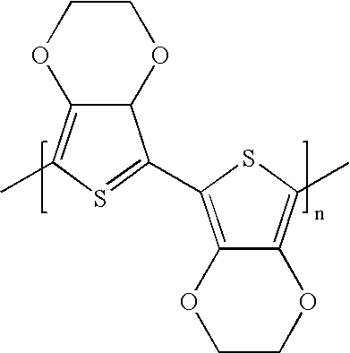
| CuPc | phthalocyanine copper |
 |
| DCJTB | 4-(dicyanomethylene)-2-(t- butyl)-6-(1,1,7,7- tetramethyljulolidyl-9-enyl)- 4H-pyran |
 |
| DCM | 4-(dicyanomethylene)-2- methyl-6-(p- dimethylaminostyryl)-4H- pyran |
 |
| Ga(Saph-q) | salicylidene-o-aminophenolato (8-quinolinoato)gallium |
 |
| H2Pc | Phthalocyanine |
 |
| |
4,4′,4″-tris(3-methyl- phenylphenylamino) triphenylamine |
 |
| NPB | N,N′-bis-(1-naphthyl)-N, N′-diphenyl-1,1′-biphenyl-4, 4′ -diamine |
 |
| PANI | Polyaniline |
 |
| PBD | 2-(4-tert-Butylphenyl)-5-(4- biphenylyl)-1,3,4-oxadiazole |
 |
| PEDOT | Polyethylene dioxythiophene |
 |
| pentacene | pentacene |
 |
| PVK | Poly(N-vinylcarbazole) |
 |
| |
5,6,11,12- tetraphenylnaphthacene |
 |
| |
2,2′2″-(1,3,5-benzenetriyl)- tris-[1-phenyl-1H- benzimidazole] |
 |
| TPD | N,N′-diphenyl-N,N′-bis(3- methylphenyl)-1,1′- biphenyl-4,4′-diamine |
 |
| VOPc | Phthalocyanine vanadium |
 |
| Zn(Ac)2 | 4-hydroxyl acridine zinc |
 |
In order to understand the present invention more clearly, some notes are listed below.
1. The emission zone of the OLEDs according to the present invention can be located in the electron-transporting layer and/or hole-transporting layer.
2. The hole-transporting layer, electron-transporting layer, buffer layer, and transitional layer mentioned in the present invention are all organic functional layers in the OLEDs.
Structural configuration of the first type of the OLEDs according to the present invention is shown in FIG. 1. Reference numeral 1 is a transparent substrate, and it can be a glass substrate or a flexible substrate made of polyethylene terephthalate (PET) and polyimide (PI) materials. Reference numeral 2 is a first electrode (anode) layer, and it can be an inorganic material electrode or organic conducting polymer electrode. The inorganic electrode is commonly made of metal oxides such as indium-tin-oxide (ITO), zinc oxide, zinc-tin-oxide, or some metals with high work function such as gold, silver, and copper. A preferable anode is ITO film. A preferable organic polymer anode in this first type is PEDOT or PANI films. Reference numeral 3 is a buffer layer of a material selected from phthalocyanine derivatives, PI derivatives, fluoropolymer, inorganic fluorine-containing salt, inorganic oxides and diamond. A preferable buffer layer material in this first type is CuPc. Reference numeral 4 is a hole-transporting layer where an organic MQW structure is used. The organic quantum well structure consists of alternating layers of the organic material A with wide energy gap and of the organic material B with narrow energy gap. And energy level of the two organic materials in the hole-transporting layer matches each other (in agreement with the above relations (I) and (II)), thus the energy level of the organic material A can enwrap the energy level of the organic material B. Potential wells of the holes and electrons are all in the organic material B due to the energy barrier at the interfaces. The organic material A is a member selected from benzidine derivatives (such as NPB, TPD, MTDATA), carbazole derivatives (such as PVK, BCP, Bphen), pyrrole derivatives and oxadiazole derivatives materials (such as TPBi, PBD). The organic material B is a kind of phthalocyanine complex such as CuPc, H2Pc, VOPc. And a preferable MQW structure in this first type is (NPB/CuPc)n. The HOMO levels of NPB and CuPc are −5.5 eV and −4.8 eV respectively, and the LUMO levels of NPB and CuPc are −2.5 eV and −2.7 eV respectively. It can be seen from the energy schematic graph (FIG. 2, FIG. 3) that the holes and electrons wells are all formed in the CuPc layers due to the energy barrier at the interfaces of NPB/CuPc layers. Reference numeral 5 is a transitional layer which can match the energy level with the electron-transporting material. A preferable transitional material is NPB in the (NPB/CuPc)n organic MQW structure light-emitting devices. Reference numeral 6 is an electron-transporting layer and it can be a metal chelate complex or an oxadiazole complex. A preferable electron-transporting material is a member selected from Alq3, Al(Saph-q), Ga(Saph-q) and Zn(Ac)2. Reference numeral 7 is a second electrode (cathode) layer, and it can be a metal material with low work function selected from Li, Mg, Ca, Sr, Al, In and their alloy with gold or copper. A preferable second electrode is a Mg:Ag alloy layer and an Ag layer. And reference numeral 8 is an electric source.
A preferable example according to the above first type of the OLEDs has the following device structure (1):
Wherein n is period number, and is an integer of 1 to 10. Generally speaking, the device of the device structure (1) is fabricated by the following procedures successively.
1. A transparent conductive ITO-coated glass substrate is cleaned ultrasonically with boiling scour water and deionized (DI) water. Then the substrate is dried under infra-red lamp. The ITO film coated on glass substrate acts as anode layer. Sheet resistance of the ITO film is about 5-100 Ω/square, and the thickness of it is about 80.0-280.0 nm.
2. The cleaned and dried ITO-coated substrate is put in the vacuum of about 1×10⁻⁵-5×10⁻³ Pa. Then a CuPc film is vapor-deposited as a buffer layer of the OLEDs on the ITO film. The deposition rate of CuPc is about 0.02-0.4 nm/s and the resulting CuPc layer thickness is about 0.5-20.0 nm.
3. A hole-transporting layer is then vapor-deposited on the CuPc buffer layer. The hole-transporting layer is an organic quantum well structure consisting of alternating NPB/CuPc layer films with the period number of n. Here, the deposition rate of CuPc is about 0.02-0.4 nm/s, and the thickness of each CuPc film is about 0.5-10.0 nm. The deposition rate of NPB is about 0.1-0.6 nm/s, and the thickness of each NPB film is about 0.5-30.0 nm.
4. A NPB film is further vapor-deposited on the hole-transporting layer as transitional layer. The deposition rate is about 0.1-0.6 nm/s, and its layer thickness is about 10.0-45.0 nm.
5. An Alq3 film is subsequently vapor-deposited on the NPB transitional layer as electron-transporting layer and electroluminescent emission layer. Here, the deposition rate of Alq3 is about 0.1-0.6 nm/s, and its layer thickness is about 40.0-100.0 nm.
6. Finally, a Mg:Ag (their deposition rate ratio is about 10:1) metal alloy layer and an Ag layer are vapor-deposited as cathode on the Alq3 layer, respectively. Here the total deposition rate of the Mg:Ag alloy layer is about 0.6-2.0 nm/s, and the total thickness of the alloy layer is about 50.0-200.0 nm. The deposition rate of the Ag layer is about 0.3-0.8 nm/s, and its layer thickness is about 40.0-200.0 nm.
Structural configuration of the second type of the OLEDs according to the present invention can also be referred to FIG. 1, except for canceling buffer layer 3. Reference numerals 1 and 2 are same as in the above first type of the OLEDs. Reference numeral 4 is a hole-transporting layer where an organic MQW structure is used. The organic quantum well structure consists of alternating layers of the organic material A with wide energy gap and the organic material C with narrow energy gap. And energy level of the two organic materials in the hole-transporting layer matches each other (in agreement with the relations (I) and (II)), thus the energy level of the organic material A can enwrap the energy level of the organic material C. Potential wells of the holes and electrons are all in the organic material C due to the energy barrier at the interfaces. The organic material A is a member selected from benzidine derivatives (such as NPB, TPD, MTDATA), carbazole derivatives (such as PVK, BCP, Bphen), pyrrole derivatives and oxadiazole derivatives materials (such as TPBi, PBD). The organic material C is a kind of dye material selected from polyphenylene derivatives (such as rubrene, pentacene), coumarin derivatives (such as C545T) and bis-pyrane derivatives (such as DCTJB, DCM). And a preferable MQW structure in this second type is (NPB/rubrene)n. The HOMO levels of NPB and rubrene are −5.5 eV and −5.4 eV respectively, and the LUMO levels of NPB and rubrene are −2.5 eV and −3.2 eV respectively. It can be seen from the energy schematic graph (FIG. 6) that the holes and electrons wells are all formed in the rubrene layers due to the energy barrier at the interfaces of NPB/rubrene films. Reference numeral 5 is a transitional layer which can match the energy level with the electron-transporting material. A preferable transitional material is NPB in the (NPB/rubrene)n organic MQW structure light-emitting devices. Reference numerals 6 and 7 are the same to that in the first type structure.
A preferable example according to the above second type of the OLEDs has the following device structure (2):
Wherein n is period number, and is an integer of 1 to 10. Generally speaking, the device of the device structure (2) is fabricated by the following procedures successively.
1. A transparent conductive ITO-coated glass substrate is cleaned ultrasonically with boiling scour water and DI water. Then the substrate is dried under infra-red lamp. The ITO film coated on glass substrate acts as anode layer. Sheet resistance of the ITO film is about 5-100 Ω/square, and the thickness of it is about 80.0-280.0 nm.
2. The cleaned and dried ITO-coated substrate is put in the vacuum of about 1×10⁻⁵-5×10⁻³ Pa. Then a hole-transporting layer is vapor-deposited on the ITO layer. The hole-transporting layer is an organic quantum well structure consisting of alternating NPB/rubrene layer films with the period number of n. Here, the deposition rate of rubrene is about 0.02-0.4 nm/s, and the thickness of each rubrene layer is about 0.5-10.0 nm. The deposition rate of NPB is about 0.1-0.6 nm/s, and the thickness of each NPB layer is about 0.5-30.0 nm.
3. A NPB film is further vapor-deposited on the hole-transporting layer as transitional layer. The deposition rate is about 0.1-0.6 nm/s, and its layer thickness is about 10.0-45.0 nm.
4. An Alq3 film is subsequently vapor-deposited on the NPB transitional layer as electron-transporting layer and electroluminescent emission layer. Here, the deposition rate of Alq3 is about 0.1-0.6 nm/s, and its layer thickness is about 40.0-100.0 nm.
5. Finally, a Mg:Ag (their deposition rate ratio is about 10:1) metal alloy layer and an Ag layer are vapor-deposited as cathode on the Alq3 layer, respectively. Here the total deposition rate of the Mg:Ag alloy layer is about 0.6-2.0 nm/s, and the total thickness of the alloy layer is about 50.0-200.0 nm. The deposition rate of the Ag layer is about 0.3-0.8 nm/s, and its layer thickness is about 40.0-200.0 nm.
Three exemplary OLEDs were fabricated in compliance with the same procedures as above described towards the device structure (1). In order to compare the device performance conveniently, the ITO layer in the three devices was kept to 200.0 nm in thickness, CuPc film (constituting the CuPc buffer layer) was kept to 6.0 nm, and NPB film (constituting the transitional layer) was kept to 15.0 nm. The thickness of the Alq3 layer as the electron transporting layer was 60.0 nm, and the thickness of the Mg:Ag alloy layer and the Ag layer was 100.0 nm respectively. Each film thickness of the alternating NPB/CuPc layer films in the three OLEDs were changed with three different period numbers n, but the total thicknesses of the NPB films and CuPc films of n periods were substantially kept to 15.0 nm and 6.0 nm respectively. The device structure configurations of the three OLEDs were shown in tables 2 and 3. Luminance-current density curve and luminance efficiency-current density curve were shown in FIG. 4 and FIG. 5 respectively.
A conventional OLED was fabricated in the same manner as described in examples 1 to 3, except that no alternating NPB/CuPc layer film was formed and the period-number n was 0 as well as total thickness of the CuPc and NPB layers was 12.0 nm and 30.0 nm respectively, as shown in table 3. The resulting device has the following device structure (3):
The following table 3 exhibited the influence of period number n on the device performances of NPB/CuPc organic quantum well light-emitting devices.
| TABLE 2 | |||
| n | Structure of OLED | ||
| C. Ex. 1 | 0 | Glass/ITO/CuPc(12.0 nm)/NPB(30.0 nm)/Alq3(60.0 nm)/Mg:Ag/Ag |
| Ex. 1 | 2 | Glass/ITO/CuPc(6.0 nm)/[NPB(7.5 nm)/CuPc(3.0 nm)]2/NPB(15.0 nm)/Alq3(60.0 nm)/Mg:Ag/Ag |
| Ex. 2 | 4 | Glass/ITO/CuPc(6.0 nm)/[NPB(3.8 nm)/CuPc(1.5 nm)]4/NPB(15.0 nm)/Alq3(60.0 nm)/Mg:Ag/Ag |
| Ex. 3 | 6 | Glass/ITO/CuPc(6.0 nm)/[NPB(2.5 nm)/CuPc(1.0 nm)]6/NPB(15.0 nm)/Alq3(60.0 nm)/Mg:Ag/Ag |
| TABLE 3 | |||||
| Comparative | Example | Example | Example | ||
| Example 1 | 1 | 2 | 3 | ||
| |
| 0 | 2 | 4 | 6 | ||
| Layer | Material | Thickness (nm) |
| Anode layer | ITO | 200.0 |
| Buffer layer | CuPc | 12.0 | 6.0 | 6.0 | 6.0 | |
| Hole-transporting | NPB | 0 | 7.5 | 3.8 | 2.5 | |
| |
0 | 3.0 | 1.5 | 1.0 | ||
| Transitional layer | NPB | 30.0 | 15.0 | 15.0 | 15.0 | |
| Electron-transporting layer | Alq3 | 60.0 | ||||
| Cathode layer | Mg:Ag | 100.0 | ||||
| Ag | 100.0 | |||||
| Device performance | Current density (A/m2) | 400 | ||||
| Luminance (cd/m2) | 1400 | 1960 | 3900 | 800 | ||
| Luminance efficiency | 3.8 | 4.3 | 9.8 | 2.3 | ||
| (cd/A) | ||||||
| Initial luminance | 1000 | |||||
| (cd/m2) | ||||||
| T1/2 (h) | 2.5 | 2.7 | 3.5 | 2 | ||
| Life time (h) | 25 | 27 | 35 | 20 | ||
It can be seen from Table 3 that the device with period number 4 achieved best characteristics. A highest efficiency of 10.8 cd/A can be obtained at current density of 34 mA/cm2. This was an improvement over previously reported result about the efficiency of the Alq3 devices without dye dopant. It is also about 3 times that of the conventional devices without an alternating NPB/CuPc layer film (n=0).
Although when period number n equaled 6, the film formation quality of the quantum well structure declined, it should be understood the reason was that the thickness of each layer was too small, leading to poor device performance. It is believed that the device performance increases with increase of the period number provided that thickness of the various layers is not so small as to cause formation difficulty of the device.
A transparent conductive ITO-coated glass substrate was cleaned ultrasonically with boiling scour water and DI water. Then the substrate was dried under infra-red lamp. The ITO film coated on glass substrate acted as anode layer. Sheet resistance of the ITO film was 15 Ω/square, and the thickness of it was 180.0 nm. The cleaned and dried ITO-coated substrate was put in the vacuum of 1×10⁻³ Pa. Then a CuPc film was vapor-deposited as a buffer layer on the ITO film. The deposition rate of CuPc was about 0.04 nm/s and the resulting layer thickness was 6.0 nm. A hole-transporting layer was further vapor-deposited on the CuPc buffer layer. The hole-transporting layer was an organic quantum well structure consisting of alternating NPB/CuPc layer films with the period number of 6. Here, the deposition rate of CuPc was 0.04 nm/s, and the thickness of each CuPc film was about 1.5 nm. The deposition rate of NPB was 0.2 nm/s, and the thickness of each NPB film was about 3.8 nm. A NPB film was subsequently vapor-deposited on the hole-transporting layer as transitional layer. The deposition rate of NPB was about 0.4 nm/s, and the resulting layer thickness was 15.0 nm. An Alq3 film was then vapor-deposited on the NPB transitional layer as electron-transporting layer and electroluminescent emission layer. Here, the deposition rate of Alq3 was 0.2 nm/s, and its layer thickness was about 60.0 nm. Finally, a Mg:Ag (their deposition rate ratio was 10:1) metal alloy layer and an Ag layer were vapor-deposited as cathode layer on the Alq3 layer, respectively. Here the total deposition rate of the Mg:Ag alloy layer was 1.5 nm/s, and the total thickness of the alloy layer was 100.0 nm. The deposition rate of the Ag layer was about 0.5 nm/s, and its layer thickness was 100.0 nm.
A turn-on voltage of 2.5V, a highest luminance of 16000 cd/m2, and a highest efficiency of 10.8 cd/A at the current density of 36 mA/cm2 were achieved by the resultant device.
A transparent conductive ITO-coated glass substrate was cleaned ultrasonically with boiling scour water and DI water. Then the substrate was dried under infra-red lamp. The ITO film coated on glass substrate acted as anode layer. Sheet resistance of the ITO film was 60 Ω/square, and the thickness of it was 100.0 nm. The cleaned and dried ITO-coated substrate was put in the vacuum of 2×10⁻³ Pa. Then a CuPc film was vapor-deposited as a buffer layer on the ITO film. The deposition rate of CuPc was about 0.06 nm/s and the resulting layer thickness was 8.0 nm. A hole-transporting layer was further vapor-deposited on the CuPc buffer layer. The hole-transporting layer was an organic quantum well structure consisting of alternating NPB/CuPc layer films with the period number of 2. Here, the deposition rate of CuPc was 0.06 nm/s, and the thickness of each CuPc film was about 3.0 nm. The deposition rate of NPB was 0.2 nm/s, and the thickness of each NPB film was about 7.5 nm. A NPB film was subsequently vapor-deposited on the hole-transporting layer as transitional layer. The deposition rate was about 0.2 nm/s, and the resulting layer thickness was 20.0 nm. An Al(Saph-q) film was then vapor-deposited on the NPB transitional layer as electron-transporting layer and electroluminescent emission layer. Here, the deposition rate of Al(Saph-q) was 0.2 nm/s, and its layer thickness was about 60.0 nm. Finally, a Mg:Ag (their deposition rate ratio was 10:1) metal alloy layer and an Ag layer were vapor-deposited as cathode on the Al(Saph-q) layer, respectively. Here the total deposition rate of the Mg:Ag alloy layer was 1.5 nm/s, and the total thickness of the alloy layer was 150.0 nm. The deposition rate of the Ag layer was about 0.4 nm/s, and its layer thickness was 50.0 nm.
A turn-on voltage of 2.8V and a highest luminance of 13000 cd/m2 were achieved by the resultant device.
A transparent conductive ITO-coated glass substrate was cleaned ultrasonically with boiling scour water and DI water. Then the substrate was dried under infra-red lamp. The ITO film coated on glass substrate acted as anode layer. Sheet resistance of the ITO film was 30 Ω/square, and the thickness of it was 140.0 nm. The cleaned and dried ITO-coated substrate was put in the vacuum of 1.5×10⁻³ Pa. Then a CuPc film was vapor-deposited as a buffer layer on the ITO film. The deposition rate was about 0.03 nm/s and the resulting layer thickness was 4.0 nm. A hole-transporting layer was further vapor-deposited on the CuPc buffer layer. The hole-transporting layer was an organic quantum well structure consisting of alternating NPB/CuPc layer films with the period number of 8. Here, the deposition rate of CuPc was 0.02 nm/s, and the thickness of each CuPc film was about 0.75 nm. The deposition rate of NPB was 0.2 nm/s, and the thickness of each NPB film was about 2.0 nm. A NPB film was subsequently vapor-deposited on the hole-transporting layer as transitional layer. The deposition rate was about 0.2 nm/s, and the resulting layer thickness was 20.0 nm. A Zn(Ac)2 film was then vapor-deposited on the NPB transitional layer as electron-transporting layer and electroluminescent emission layer. Here, the deposition rate of Zn(Ac)2 was 0.2 nm/s, and its layer thickness was about 60.0 nm. Finally, a Mg:Ag (their deposition rate ratio was 10:1) metal alloy layer and an Ag layer were vapor-deposited as cathode on the Zn(Ac)2 layer, respectively. Here the total deposition rate of the Mg:Ag alloy layer was 1.5 nm/s, and the total thickness of the alloy layer was 180.0 nm. The deposition rate of the Ag layer was about 0.5 nm/s, and its layer thickness was 50.0 nm.
A turn-on voltage of 2.9V and a highest luminance of 12000 cd/m2 were achieved by the resultant device.
Three exemplary OLEDs were fabricated in compliance with the same procedure as above described towards the device structure (2). In order to compare the device performance conveniently, thickness of the ITO film in the devices was kept to 240.0 nm, and total thickness of NPB film (including transitional layer) was kept to 40.0 nm. Total thickness of n-layers of the alternating rubrene films was substantially kept to 8.0 nm, but each NPB film was constantly kept to 5.0 nm. The thickness of Alq3 layer was 60.0 nm, and the thickness of the Mg:Ag alloy layer and the Ag layer was 100.0 nm respectively. But alternating NPB/rubrene layer films in the three OLEDs were changed with three different period numbers n. The device structures of the three OLEDs were shown in tables 4 and 5. Luminance-current density curve and luminance efficiency-current density curve were shown in FIG. 7 and FIG. 8 respectively.
A conventional OLED was fabricated in the same manner as described in examples 7 to 9, except that no alternating NPB/rubrene layer film was formed and the period number n was 0. The resulting device had the following device structure (4), also as shown in table 4. Thickness of the NPB layer was 40.0 nm.
| TABLE 4 | |||
| n | Structure of OLED | ||
| C. Ex. 2 | 0 | Glass/ITO/NPB(40.0 nm)/Alq3(60.0 nm)/Mg:Ag/Ag |
| Ex. 7 | 2 | Glass/ITO/[NPB(5.0 nm)/rubrene(4.0 nm)]2/NPB(30.0 nm)/Alq3(60.0 nm)/Mg:Ag/Ag |
| Ex. 8 | 4 | Glass/ITO/[NPB(5.0 nm)/rubrene(2.0 nm)]4/NPB(20.0 nm)/Alq3(60.0 nm)/Mg:Ag/Ag |
| Ex. 9 | 6 | Glass/ITO/[NPB(5.0 nm)/rubrene(1.3 nm)]6/NPB(10.0 nm)/Alq3(60.0 nm)/Mg:Ag/Ag |
A conventional OLED was fabricated in the same manner as described in examples 7 to 9, except that no alternating NPB/rubrene layer film was formed and the period number n was 0, but the electron-transporting layer consisted of 60.0 nm Alq3 layer doped with 2 wt % rubrene. The resulting device had the following device structure (5), also as shown in table 5.
The EL spectra of the above OLEDs were shown in FIG. 9. The curves (a), (b), (c) and (d) corresponded to organic quantum well light-emitting devices with the period number of 0, 2, 4 and 6 respectively. The curve (e) corresponded to the device of the above device structure (5) and showed a yellow light emission originated from rubrene. In the NPB/rubrene MQW structure according to the invention, a distinct shift of the emitting spectrum had been observed with increase of the period number n. Here, the n=0 device (curve a) showed pure Alq3 emission characteristics, while the n=2 device (curve b) and the n=4 device (curve c) showed emission characteristics of rubrene with a small Alq3 emission component as a shoulder at 520 nm. It was interesting to point out that the n=6 device (curve d) showed pure rubrene emission characteristics which were the same as the conventional device without MQW structure (curve e), and Alq3 emission was hardly visible, indicating that the carrier recombination were confined in the rubrene layers only.
The EL spectra study revealed that the MQW structure can not only adjust the holes mobility in the devices, but also control the emitting zone and output wavelength in the devices due to the hole distribution and confinement in the MQW structures.
In summary, when introduced into OLEDs as a hole-transporting layer, organic MQW of NPB/rubrene can efficiently control the hole mobility and help to achieve hole-electron balance. Dye material is vapor-deposited as a separate layer in the present invention. The EL spectra study reveals that the MQW structure can even control emitting zone in the devices due to the hole distribution and confinement in the MQW structures. This work may provide useful clues on how to obtain different emission colors from the OLEDs.
Table 5 exhibited the influence of period number n on device performance of NPB/rubrene organic quantum well light-emitting devices.
| TABLE 5 | ||||||
| C. Ex. | Example | Example | Example | C. Ex. | ||
| 2 | 7 | 8 | 9 | 3 | ||
| |
| 0 | 2 | 4 | 6 | 0 | ||
| Layer | Material | Thickness (nm) |
| Anode layer | ITO | 240.0 |
| Hole-transporting | |
0 | 5.0 | 5.0 | 5.0 | 0 | |
| | rubrene | 0 | 4.0 | 2.0 | 1.3 | 0 | |
| Transitional layer | NPB | 40.0 | 30.0 | 20.0 | 10.0 | 40.0 | |
| Electron-transporting | Alq3 | 60.0 | 60.0 | 60.0 | 60.0 | 60.0 | |
| layer | (2 wt % rubrene- | ||||||
| doped) | |||||||
| Cathode layer | Mg:Ag | 100.0 | |||||
| Ag | 100.0 | ||||||
| Device performance | Current | 3000 | |||||
| density(A/m2) | |||||||
| Luminance | 6160 | 9000 | 17800 | 13500 | |||
| (cd/m2) | |||||||
| Luminance | 2.01 | 3.03 | 6.00 | 4.46 | |||
| efficiency (cd/A) | |||||||
| Wavelength (nm) | 528 | 548 | 556 | 560 | 564 | ||
It can be seen from Table 5 that the OLED with period number 4 showed the best luminance and efficiency. When period number was 6, each layer in the organic quantum well was too thin, the film quality became poor, even it was possible to destroy the uniform quantum well structure, and the device efficiency decreased. In fact, it was expected to enhance the device efficiency by increasing the period number if multiple quantum structure was not destroyed. It was interesting to find that, with the increase of period number n, the proportion of rubrene emission in the EL spectrum became higher, and the emission color showed a red shift. This proved that the emission zone in the device transferred to rubrene layer with the increase of period number. The larger period number n is, the more light rubrene layer emits.
Examples 10 to 13 were carried out according to the same manner and procedures as in the examples 7 to 9, except that the period numbers kept constantly at 4, and the device structures of the resulting OLEDs were shown in table 6. Meanwhile, the following table 6 also exhibited the influence of NPB thickness on device performance of NPB/rubrene organic quantum well light-emitting devices.
| TABLE 6 | |||||
| Example 10 | Example 11 | Example 12 | Example 13 | ||
| |
||
| Layer | Material | Thickness (nm) |
| Anode layer | ITO | 240.0 |
| Hole-transporting | NPB | 1.0 | 3.0 | 5.0 | 7.0 |
| layer | rubrene | 2.0 | |||
| Transitional layer | NPB | 36.0 | 28.0 | 20.0 | 12.0 |
| Electron-transporting | Alq3 | 60.0 | |||
| layer | |||||
| Cathode layer | Mg:Ag | 100.0 | |||
| Ag | 100.0 | ||||
| Device performance | Current density | 3000 | |||
| (A/m2) | |||||
| Luminance (cd/m2) | 15000 | 24000 | 18000 | 17400 | |
| Luminance | 5.00 | 8.00 | 6.00 | 5.80 | |
| efficiency (cd/A) | |||||
It can be seen from table 6 that the OLEDs showed best performance with 3.0 nm thickness of the NPB layers. When thickness was 1.0 nm, the performances became worse due to poor film quality in the organic quantum well structure. Generally speaking, the smaller thickness of NPB layer leads to a higher performance.
Examples 14 to 17 were carried out according to the same manner and procedures as in the examples 7 to 9, except that the period numbers kept constantly at 4, and the device structures of the resulting OLEDs were shown in table 7. Meanwhile, the following table 7 also exhibited the influence of rubrene thickness on device performance of the NPB/rubrene organic quantum well light-emitting devices.
| TABLE 7 | |||||
| Example 14 | Example 15 | Example 16 | Example 17 | ||
| |
||
| Layer | Material | Thickness (nm) |
| Anode layer | ITO | 240.0 |
| Hole-transporting | NPB | 5.0 |
| layer | rubrene | 1.0 | 2.0 | 4.0 | 6.0 |
| Transitional layer | NPB | 20.0 | |||
| Electron-transporting | Alq3 | 60.0 | |||
| layer | |||||
| Cathode layer | Mg:Ag | 100.0 | |||
| Ag | 100.0 | ||||
| Device performance | Current density | 3000 | |||
| (A/m2) | |||||
| Luminance | 10500 | 18000 | 15000 | 15000 | |
| (cd/m2) | |||||
| Luminance | 3.50 | 6.00 | 5.00 | 5.00 | |
| efficiency (cd/A) | |||||
It can be seen from table 7 that the influence of rubrene thickness on device performance of NPB/rubrene organic quantum well light-emitting devices was not obvious. Only when the thickness of the rubrene layer was as low as 1.0 nm, the organic quantum well structure was destroyed. Relatively thin films can be obtained by choosing appropriate fabrication conditions. A preferable thickness is 2.0 nm.
Examples 18 to 21 were carried out according to the same manner and procedures as in examples 7 to 9, except that the period number kept constantly at 4, and the device structures of the resulting OLEDs were shown in Table 8.
The following table 8 exhibited the influence of different electron-transporting materials and MQW structure materials on device performance of the organic quantum well light-emitting devices.
| TABLE 8 | |||||
| Example 18 | Example 19 | Example 20 | Example 21 | ||
| |
||
| Layer | Material | Thickness (nm) |
| Anode layer | ITO | 240.0 |
| Hole-transporting layer | NPB barrier | 5.0 | 5.0 | 5.0 | 5.0 |
| Well | Material | CuPc | rubrene | rubrene | DCJTB | |
| 2.0 | 2.0 | 2.0 | 2.0 |
| Transitional layer | NPB | 20.0 | 20.0 | 20.0 | 20.0 |
| Electron-transporting layer | Material | Alq3 | Alq3 | Al(Saph-q) | Ga(Saph-q) |
| 60.0 | 60.0 | 60.0 | 60.0 | ||
| Cathode | Mg:Ag | 100.0 | |||
| Ag | 100.0 | ||||
| Device performance | Current density | 3000 | |||
| (A/m2) | |||||
| Luminance (cd/m2) | 22000 | 17800 | 25800 | 9500 | |
| Luminance | 7.03 | 5.90 | 8.60 | 3.17 | |
| efficiency (cd/A) | |||||
| Wavelength (nm) | 528 | 550 | 560 | 620 | |
Examples 22 to 24 were carried out according to the same manner and procedures as in examples 7 to 9, except for the device structures of the resulting OLEDs were shown in table 9.
An OLED was fabricated in the same manner as described in examples 22 to 24, except that no alternating NPB/rubrene layer film was formed and the period number n was 0, and the remaining structure configurations of the resulting OLED being shown in table 9.
Meanwhile, table 9 exhibited also the influence of period number n on device performance of the NPB/rubrene organic quantum well light-emitting devices.
| TABLE 9 | |||||
| C. Example 4 | Example 22 | Example 23 | Example 24 | ||
| |
| 0 | 2 | 4 | 6 | ||
| Layer | Material | Thickness (nm) |
| Anode layer | ITO | 240.0 |
| Hole-transporting | |
0 | 5.0 | 5.0 | 5.0 | |
| | rubrene | 0 | 8.0 | 2.0 | 1.3 | |
| Transitional layer | NPB | 40.0 | 35.0 | 20.0 | 10.0 | |
| Electron-transporting | Alq3 | 60.0 | ||||
| layer | ||||||
| Cathode layer | Mg:Ag | 100.0 | ||||
| Ag | 100.0 | |||||
| Device performance | Initial luminance | 1000 | ||||
| (cd/m2) | ||||||
| T1/2 (h) | 2.5 | 2.4 | 2.6 | 1.5 | ||
| Life time (h) | 25 | 24 | 26 | 15 | ||
A transparent conductive ITO-coated glass substrate was cleaned ultrasonically with boiling scour water and DI water. Then the substrate was dried under infra-red lamp. The ITO film coated on glass substrate acted as anode layer. Sheet resistance of the ITO film was 60 Ω/square, and the thickness of it was 100.0 nm. The cleaned and dried ITO-coated substrate was put in the vacuum of 2×10⁻³ Pa. Then a hole-transporting layer was vapor-deposited on the ITO layer. The hole-transporting layer was an organic quantum well structure consisting of alternating NPB/rubrene layer films with the period number of 4. Here, the deposition rate of rubrene was 0.1 nm/s, and the thickness of each rubrene film was about 2.0 nm. The deposition rate of NPB was 0.2 nm/s, and the thickness of each NPB film was about 5.0 nm. A NPB film was further vapor-deposited on the hole-transporting layer as transitional layer. The deposition rate was about 0.2 nm/s, and its thickness was 20.0 nm. An Al(Saph-q) film was subsequently vapor-deposited on the NPB transitional layer as electron-transporting layer and electroluminescent emission layer. Here, the deposition rate of Al(Saph-q) was 0.2 nm/s, and its layer thickness was about 60.0 nm. Finally, a Mg:Ag (their deposition rate ratio was 10:1) metal alloy layer and an Ag layer were vapor-deposited as cathode layer on the Al(Saph-q) layer, respectively. Here the total deposition rate of the Mg:Ag alloy layer was 15 nm/s, and the total thickness of the alloy layer was 150.0 nm. The deposition rate of the Ag layer was about 0.4 nm/s, and its layer thickness was 50.0 nm.
A turn-on voltage of 2.8V and a highest luminance of 16000 cd/m2 were achieved by the resultant device.
A transparent conductive ITO-coated glass substrate was cleaned ultrasonically with boiling scour water and DI water. Then the substrate was dried under infra-red lamp. The ITO film coated on glass substrate acted as anode layer. Sheet resistance of the ITO film was 15 Ω/square, and the thickness of it was 260.0 nm. The cleaned and dried ITO-coated substrate was put in the vacuum of 1×10⁻³ Pa. Then a CuPc film was vapor-deposited as buffer layer on the ITO film. The deposition rate of CuPc was about 0.02 nm/s and the resulting thickness was 10.0 nm. A hole-transporting layer was further vapor-deposited on the CuPc buffer layer. The hole-transporting layer was an organic quantum well structure consisting of alternating NPB/rubrene layer films with the period number of 3. Here, the deposition rate of rubrene was 0.1 nm/s, and the thickness of each rubrene film was about 2.0 nm. The deposition rate of NPB was 0.2 nm/s, and the thickness of each NPB film was about 5.0 nm. A NPB film was subsequently vapor-deposited on the hole-transporting layer as transitional layer. The deposition rate was about 0.2 nm/s, and its thickness was 20.0 nm. An Al(Saph-q) film was then vapor-deposited on the NPB transitional layer as electron-transporting layer and electroluminescent emission layer. Here, the deposition rate of Al(Saph-q) was 0.2 nm/s, and its layer thickness was about 60.0 nm. Finally, a Mg:Ag (their deposition rate ratio was 10:1) metal alloy layer and an Ag layer were vapor-deposited as cathode layer on the Al(Saph-q) layer, respectively. Here the total deposition rate of the Mg:Ag alloy layer was 1.5 nm/s, and the total thickness of the alloy layer was 150.0 nm. The deposition rate of the Ag layer was about 0.4 nm/s, and its layer thickness was 50.0 nm.
A turn-on voltage of 2.5V and a highest luminance of 26000 cd/m2 were achieved by the resultant device.
A transparent conductive ITO-coated glass substrate was cleaned ultrasonically with boiling scour water and DI water. Then the substrate was dried under infra-red lamp. The ITO film coated on glass substrate acts as anode layer. Sheet resistance of the ITO film was 100 Ω/square, and the thickness of it was 60.0 nm. The cleaned and dried ITO-coated substrate was put in the vacuum of 2×10⁻³ Pa. Then a hole-transporting layer was vapor-deposited on the ITO layer. The hole-transporting layer was an organic quantum well structure consisting of alternating MTDATA/rubrene layer films with the period number of 10. Here, the deposition rate of rubrene was 0.1 nm/s, and the thickness of each rubrene film was about 2.0 nm. The deposition rate of MTDATA was 0.2 nm/s, and the thickness of each MTDATA film was about 5.0 nm. A NPB film was further vapor-deposited on the hole-transporting layer as transitional layer. The deposition rate was about 0.2 nm/s, and its thickness was 5.0 nm. An Alq3 film was subsequently vapor-deposited on the NPB transitional layer as electron-transporting layer and electroluminescent emission layer. Here, the deposition rate of Alq3 was 0.2 nm/s, and its layer thickness was about 60.0 nm. Finally, a Mg:Ag (their deposition rate ratio was 10:1) metal alloy layer and an Ag layer were vapor-deposited as cathode layer on the Alq3 layer, respectively. Here the total deposition rate of the Mg:Ag alloy layer was 1.5 nm/s, and the total thickness of the alloy layer was 150.0 nm. The deposition rate of the Ag layer was about 0.4 nm/s, and its layer thickness was 50.0 nm.
A turn-on voltage of 2.8V and a highest luminance of 14000 cd/m2 were achieved by the resultant device.
A transparent conductive ITO-coated glass substrate was cleaned ultrasonically with boiling scour water and DI water. Then the substrate was dried under infra-red lamp. The ITO film coated on glass substrate acted as anode layer. Sheet resistance of the ITO film was 60 Ω/square, and the thickness of it was 100.0 nm. The cleaned and dried ITO-coated substrate was put in the vacuum of 2×10⁻³ Pa. Then a hole-transporting layer was vapor-deposited on the ITO layer. The hole-transporting layer was an organic quantum well structure consisting of alternating TPD/DCJTB layer films with the period number of 4. Here, the deposition rate of DCJTB was 0.1 nm/s, and the thickness of each DCJTB film was about 2.0 nm. The deposition rate of TPD was 0.2 nm/s, and the thickness of each TPD film was about 5.0 nm. A TPD film was further vapor-deposited on the hole-transporting layer as transitional layer. The deposition rate was about 0.2 nm/s, and its thickness was 20.0 nm. An Alq3 film was subsequently vapor-deposited on the TPD transitional layer as electron-transporting layer and electroluminescent emission layer. Here, the deposition rate of Alq3 was 0.2 nm/s, and its layer thickness was about 60.0 nm. Finally, a Mg:Ag (their deposition rate ratio was 10:1) metal alloy layer and an Ag layer were vapor-deposited as cathode layer on the Alq3 layer, respectively. Here the total deposition rate of the Mg:Ag alloy layer was 1.5 nm/s, and the total thickness of the alloy layer was 150.0 nm. The deposition rate of the Ag layer was about 0.4 nm/s, and its layer thickness was 50.0 nm.
A turn-on voltage of 2.8V and a highest luminance of 12000 cd/m2 were achieved by the resultant device.
A transparent conductive ITO-coated glass substrate was cleaned ultrasonically with boiling scour water and DI water. Then the substrate was dried under infra-red lamp. The ITO film coated on glass substrate acted as anode layer. Sheet resistance of the ITO film was 40 Ω/square, and the thickness of it was 150.0 nm. The cleaned and dried ITO-coated substrate was put in the vacuum of 1×10⁻³ Pa. Then a hole-transporting layer was vapor-deposited on the ITO layer. The hole-transporting layer was an organic quantum well structure consisting of alternating MTDATA/rubrene layer films with the period number of 4. Here, the deposition rate of rubrene was 0.2 nm/s, and the thickness of each rubrene film was about 2.0 nm. The deposition rate of MTDATA was 0.2 nm/s, and the thickness of each MTDATA film was about 5.0 nm. A MTDATA film was further vapor-deposited on the hole-transporting layer as transitional layer. For this transitional layer, the deposition rate was about 0.2 nm/s, and the resulting thickness was 20.0 nm. An Alq3 film was vapor-deposited on the MTDATA transitional layer as electron-transporting layer and electroluminescent emission layer. Here, the deposition rate of Alq3 was 0.2 nm/s, and its layer thickness was about 60.0 nm. Finally, a Mg:Ag (their deposition rate ratio was 10:1) metal alloy layer and an Ag layer were vapor-deposited as cathode layer on the Alq3 layer, respectively. Here the total deposition rate of the Mg:Ag alloy layer was 1.5 nm/s, and the total thickness of the alloy layer was 150.0 nm. The deposition rate of the Ag layer was about 0.4 nm/s, and its layer thickness was 50.0 nm.
A turn-on voltage of 2.8V and a highest luminance of 18000 cd/m2 were achieved by the resultant device.
A transparent conductive ITO-coated glass substrate was cleaned ultrasonically with boiling scour water and DI water. Then the substrate was dried under infra-red lamp. The ITO film coated on glass substrate acted as anode layer. Sheet resistance of the ITO film was 10 Ω/square, and the thickness of it was 280.0 nm. The cleaned and dried ITO-coated substrate was put in the vacuum of 4×10⁻³ Pa. Then a hole-transporting layer was vapor-deposited on the ITO layer. The hole-transporting layer was an organic quantum well structure consisting of alternating NPB/C545T layer films with the period number of 4. Here, the deposition rate of C545T was 0.1 nm/s, and the thickness of each C545T film was about 2.0 nm. The deposition rate of NPB was 0.2 nm/s, and the thickness of each NPB film was about 5.0 nm. A NPB film was further vapor-deposited on the hole-transporting layer as transitional layer. The deposition rate of NPB was about 0.2 nm/s, and the resulting thickness was 20.0 nm. An Alq3 film was vapor-deposited on the NPB transitional layer as electron-transporting layer and electroluminescent emission layer. Here, the deposition rate of Alq3 was 0.2 nm/s, and its layer thickness was about 60.0 nm. Finally, a Mg:Ag (their deposition rate ratio was 10:1) metal alloy layer and an Ag layer were vapor-deposited as cathode layer on the Alq3 layer, respectively. Here the total deposition rate of the Mg:Ag alloy layer was 1.5 nm/s, and the total thickness of the alloy layer was 150.0 nm. The deposition rate of the Ag layer was about 0.4 nm/s, and its layer thickness was 50.0 nm.
A turn-on voltage of 2.5V and a highest luminance of 28000 cd/m2 were achieved by the resultant device.
A transparent conductive ITO-coated glass substrate was cleaned ultrasonically with boiling scour water and DI water. Then the substrate was dried under infra-red lamp. The ITO film coated on glass substrate acted as anode layer. Sheet resistance of the ITO film was 20 Ω/square, and the thickness of it was 220.0 nm. The cleaned and dried ITO-coated substrate was put in the vacuum of 3×10⁻³ Pa. Then a hole-transporting layer was vapor-deposited on the ITO layer. The hole-transporting layer was an organic quantum well structure consisting of alternating MTDATA/DCM layer films with the period number of 5. Here, the deposition rate of DCM was 0.05 nm/s, and the thickness of each DCM film was about 2.0 nm. The deposition rate of MTDATA was 0.1 nm/s, and the thickness of each MTDATA was about 5.0 nm. A NPB film was further vapor-deposited on the hole-transporting layer as transitional layer. The deposition rate was about 0.2 nm/s, and its thickness was 20.0 nm. A Bphen film was subsequently vapor-deposited on the NPB transitional layer as electron-transporting layer. Here, the deposition rate of Bphen was 0.2 nm/s, and its layer thickness was about 60.0 nm. Finally, a Mg:Ag (their deposition rate ratio was 10:1) metal alloy layer and an Ag layer were vapor-deposited as the cathode on Bphen layer, respectively. Here the total deposition rate of the Mg:Ag alloy layer was 1.5 nm/s, and the total thickness of the alloy layer was 150.0 nm. The deposition rate of the Ag layer was about 0.4 nm/s, and its layer thickness was 50.0 nm.
A turn-on voltage of 2.5V and a highest luminance of 28000 cd/m2 were achieved by the resultant device.
While this invention has been described in terms of some preferred examples, it should also be understood that there are alterations, permutations, and equivalents which fall within the scope of this invention.
Claims (15)
1. An organic light-emitting device comprising:
a transparent substrate;
a first electrode layer;
a second electrode layer;
a hole-transporting layer; and
a electron-transporting layer sandwiched between the first electrode layer and second electrode layer;
wherein,
the hole-transporting layer includes an organic multiple-quantum-well structure, and the multiple-quantum-well structure has a period number of alternating layers formed of a layer of organic material A with wide energy gap and a layer of organic material B with narrow energy gap;
highest energy occupied molecular orbital levels of the organic material A are lower than highest energy occupied molecular orbital levels of the organic material B; and
lowest energy unoccupied molecular orbital levels of the organic material A are higher than lowest energy unoccupied molecular orbital levels of the organic material B.
2. The organic light-emitting device of claim 1 , wherein the period number of multiple-quantum-well structure is an integer of 1 to 10.
3. The organic light-emitting device of claim 1 , wherein the organic material A layer is in the range of about 0.5 to 30.0 nm in thickness, and the organic material B layer is in the range of about 0.5 to 10.0 nm in thickness.
4. The organic light-emitting device of claim 1 , wherein the organic material B is a dye material.
5. The organic light-emitting device of claim 2 , wherein the organic material B is a dye material.
6. The organic light-emitting device of claim 1 , wherein:
a buffer layer is introduced between the first electrode layer and the hole-transporting layer; and
a transitional layer is introduced between the hole-transporting layer and the electron-transporting layer.
7. The organic light-emitting device of claim 6 , wherein:
the buffer layer is formed by phthalocyanine copper material; and the transitional layer is formed by N,N′-bis-(1-naphthyl)-N,N′-diphenyl-1,1′-biphenyl-4,4′-diamine material.
8. The organic light-emitting device of claim 1 , wherein:
the organic material A is a material selected from the group consisting of benzidine derivatives, carbazole derivatives, pyrrole derivatives and oxadiazole derivatives; and
the organic material B is a phthalocyanine complex.
9. The organic light-emitting device of claim 8 , wherein:
the benzidine derivatives include;
N,N′-bis-(1-naphthyl)-N,N′-diphenyl-1,1′-biphenyl-4,4′-diamine;
N,N′-diphenyl-N,N′-bis(3-methylphenyl)-1,1′-biphenyl-4,4′-diamine; and
4,4′,4″-tris(3-methyl-phenylphenylamino) triphenylamine;
the carbazole derivatives include;
poly (N-vinylcarbazole);
2,9-dimethyl-4,7-diphenyl-1,10-phenanthroline;
4,7-diphenyl-1,10-phenanthroline;
the oxadiazole derivatives include;
2,2′,2″-(1,3,5-benzenetriyl)-tris-[1-phenyl-1H-benzimidazole]; and
2-(4-tert-Butylphenyl)-5-(4-biphenylyl)-1,3,4-oxadiazole; and
the phthalocyanine complex includes at least one of;
phthalocyanine copper;
phthalocyanine; and
phthalocyanine vanadium.
10. The organic light-emitting device of claim 8 , wherein:
the organic material A is N,N′-bis-(1-naphthyl)-N,N′-diphenyl-1,1′-biphenyl-4,4′-diamine; and
the organic material B is phthalocyanine copper.
11. The organic light-emitting device of claim 1 , wherein the electron-transporting layer is formed by at least one of a metal chelate complex and a oxadiazole complex.
12. The organic light-emitting device of claim 11 , wherein the metal chelate complex is a material selected from the group consisting of:
tris(8-hydroxyquinoline) aluminum;
salicylidene-o-aminophenolato (8-quinolinoato) aluminum;
salicylidene-o-aminophenolato (8-quinolinoato) gallium; and
4-hydroxyl acridine zinc.
13. The organic light-emitting device of claim 4 , wherein:
the organic material A is a material selected from the group consisting of benzidine derivatives, carbazole derivatives, pyrrole derivatives and oxadiazole derivatives; and
the dye material is a material selected from the group consisting of polyphenylene derivatives, coumarin derivatives and bis-pyrane derivatives.
14. The organic light-emitting device of claim 13 , wherein:
the polyphenylene derivatives include;
5,6,11,12-tetraphenylnaphthacene; and
pentacene;
the coumarin derivatives include 10-(2-benzothiazolyl)-1,1,7,7-tetramethyl-2,3,6,7-tetrahydro-1H,5H,11H-[1]benzopyrano[6,7,8-ij]quinolizin-11-one; and
the bis-pyrane derivatives include;
4-(dicyanomethylene)-2-(t-butyl)-6-(1,1,7,7-tetramethyljulolidyl-9-enyl)-4H-pyran; and
4-(dicyanomethylene)-2-methyl-6-(p-dimethylaminostyryl)-4H-pyran.
15. The organic light-emitting device of claim 13 , wherein:
the organic material A is N,N′-bis-(1-naphthyl)-N,N′-diphenyl-1,1′-biphenyl-4,4′-diamine; and
the dye material is 5,6,11,12-tetraphenylnaphthacene.
Applications Claiming Priority (6)
| Application Number | Priority Date | Filing Date | Title |
|---|---|---|---|
| CN02116537A | 2002-04-03 | ||
| CN02116537.8 | 2002-04-03 | ||
| CN02116537A CN1409412A (en) | 2002-04-03 | 2002-04-03 | Organic electroluminescence device using organic quantum trap as hole transmission layer |
| CN02125484.2 | 2002-08-13 | ||
| CN02125484A | 2002-08-13 | ||
| CN 02125484 CN1398146A (en) | 2002-08-13 | 2002-08-13 | Electroluminescent organic device |
Publications (2)
| Publication Number | Publication Date |
|---|---|
| US20030197465A1 US20030197465A1 (en) | 2003-10-23 |
| US6806491B2 true US6806491B2 (en) | 2004-10-19 |
Family
ID=29216720
Family Applications (1)
| Application Number | Title | Priority Date | Filing Date |
|---|---|---|---|
| US10/351,070 Expired - Lifetime US6806491B2 (en) | 2002-04-03 | 2003-01-24 | Organic light-emitting devices |
Country Status (2)
| Country | Link |
|---|---|
| US (1) | US6806491B2 (en) |
| JP (1) | JP3615536B2 (en) |
Cited By (16)
| Publication number | Priority date | Publication date | Assignee | Title |
|---|---|---|---|---|
| US20050110009A1 (en) * | 2003-08-27 | 2005-05-26 | Jan Blochwitz-Nimoth | Light-emitting component and process for its preparation |
| US20060132026A1 (en) * | 2004-12-17 | 2006-06-22 | Honeywell International, Inc. | Organic light emitting diode (OLED) having improved stability, luminance, and efficiency |
| US20060133437A1 (en) * | 2004-12-21 | 2006-06-22 | Trustees Of Princeton University | Organic injection laser |
| US20060244373A1 (en) * | 2005-04-28 | 2006-11-02 | Semiconductor Energy Laboratory Co., Ltd. | Light emitting device and method for manufacturing thereof |
| US20070103067A1 (en) * | 2005-11-08 | 2007-05-10 | Ya-Ping Tsai | Organic electroluminescence device and electron transporting layer |
| US20070248840A1 (en) * | 2006-04-20 | 2007-10-25 | Wintek Corporation | Organic electroluminescent device |
| US20070269916A1 (en) * | 2006-05-22 | 2007-11-22 | Tae-Whan Kim | Organic light emitting diode display and manufacturing method |
| US20080142794A1 (en) * | 2006-12-04 | 2008-06-19 | Satoko Shitagaki | Light-emitting element, light-emitting device, and electronic device |
| US20090085474A1 (en) * | 2007-09-27 | 2009-04-02 | Semiconductor Energy Laboratory Co., Ltd. | Light-Emitting Element, Light-Emitting Device, and Electronic Appliance |
| US20090206732A1 (en) * | 2005-07-06 | 2009-08-20 | Semiconductor Energy Laboratory Co., Ltd. | Light-Emitting Element, Light-Emitting Device, and Electronic Device |
| US20100252821A1 (en) * | 2007-07-12 | 2010-10-07 | Dong Kyu Park | Multilayer polymer electroluminescent device comprising water-soluble polymer layer containing cations and method for fabricating the same |
| US20100327309A1 (en) * | 2006-12-12 | 2010-12-30 | Koninklijke Philips Electronics N.V. | Voltage-operated layered arrangement |
| US8125144B2 (en) | 2005-04-11 | 2012-02-28 | Semiconductor Energy Laboratory Co., Ltd. | Light-emitting element, light-emitting device, and vapor deposition apparatus |
| US20120091436A1 (en) * | 2010-10-13 | 2012-04-19 | The Regents Of The University Of Michigan | Ordered organic-organic multilayer growth |
| US20120205633A1 (en) * | 2011-02-11 | 2012-08-16 | Semiconductor Energy Laboratory Co., Ltd. | Light-Emitting Device and Manufacturing Method Thereof |
| US9159944B2 (en) | 2012-12-20 | 2015-10-13 | Industrial Technology Research Institute | White organic light-emitting diodes |
Families Citing this family (21)
| Publication number | Priority date | Publication date | Assignee | Title |
|---|---|---|---|---|
| US7560175B2 (en) | 1999-12-31 | 2009-07-14 | Lg Chem, Ltd. | Electroluminescent devices with low work function anode |
| KR100377321B1 (en) | 1999-12-31 | 2003-03-26 | 주식회사 엘지화학 | Electronic device comprising organic compound having p-type semiconducting characteristics |
| KR100721656B1 (en) | 2005-11-01 | 2007-05-23 | 주식회사 엘지화학 | Organic electronic devices |
| JP4060113B2 (en) * | 2002-04-05 | 2008-03-12 | 株式会社半導体エネルギー研究所 | Light emitting device |
| KR101246247B1 (en) * | 2003-08-29 | 2013-03-21 | 가부시키가이샤 한도오따이 에네루기 켄큐쇼 | Electroluminescent device and light-emitting device including the same |
| US7776456B2 (en) * | 2004-12-03 | 2010-08-17 | Universal Display Corporation | Organic light emitting devices with an emissive region having emissive and non-emissive layers and method of making |
| US7745019B2 (en) * | 2005-04-28 | 2010-06-29 | Semiconductor Energy Laboratory Co., Ltd. | Light emitting element and light emitting device and method of manufacturing light emitting element |
| JP4801495B2 (en) * | 2005-04-28 | 2011-10-26 | 株式会社半導体エネルギー研究所 | Light emitting element and light emitting device |
| JP4999291B2 (en) * | 2005-06-30 | 2012-08-15 | 三洋電機株式会社 | ORGANIC ELECTROLUMINESCENCE ELEMENT AND DISPLAY DEVICE OR LIGHT EMITTING DEVICE INCLUDING THE SAME |
| KR100696961B1 (en) | 2005-08-22 | 2007-03-20 | 한양대학교 산학협력단 | Organic light emitting devices operating in yellow spectrum region and preparation method thereof |
| KR100720100B1 (en) * | 2005-08-23 | 2007-05-18 | 한양대학교 산학협력단 | Organic light emitting devices having hole blocking layer utilizing multiple hetero-structure and preparation method thereof |
| US20070048545A1 (en) * | 2005-08-31 | 2007-03-01 | Eastman Kodak Company | Electron-transporting layer for white OLED device |
| KR100646795B1 (en) * | 2005-09-08 | 2006-11-23 | 한양대학교 산학협력단 | Organic light emitting devices comprising hole transporting layer doped stepwise and preparation method thereof |
| EP1780816B1 (en) * | 2005-11-01 | 2020-07-01 | Novaled GmbH | A method for producing an electronic device with a layer structure and an electronic device |
| EP1798306B1 (en) * | 2005-12-07 | 2008-06-11 | Novaled AG | Method of vapour deposition |
| CN101371619B (en) | 2006-01-18 | 2013-11-13 | Lg化学株式会社 | OLED having stacked organic light-emitting units |
| TWI353677B (en) | 2006-03-21 | 2011-12-01 | Novaled Ag | Method for preparing doped organic semiconductor m |
| EP2091097A3 (en) * | 2008-02-13 | 2013-05-15 | Semiconductor Energy Laboratory Co, Ltd. | Light-emitting element, light-emitting device, and electronic device |
| KR101652789B1 (en) | 2009-02-23 | 2016-09-01 | 삼성전자주식회사 | Quantum dot light emitting device having quantum dot multilayer |
| EP2481104A1 (en) * | 2009-09-24 | 2012-08-01 | Empa | Multi layer organic thin film solar cell |
| KR102516591B1 (en) | 2016-02-05 | 2023-03-31 | 삼성디스플레이 주식회사 | Light emitting diode and display device including the same |
-
2003
- 2003-01-24 US US10/351,070 patent/US6806491B2/en not_active Expired - Lifetime
- 2003-04-03 JP JP2003100660A patent/JP3615536B2/en not_active Expired - Lifetime
Non-Patent Citations (6)
| Title |
|---|
| C. W. Tang and S. A. VanSlyke, "Organic electroluminescent diodes," Appl. Phys. Lett., No. 51, vol. 2, Sep. 1997, pp. 913-915. |
| Hany Aziz and Zoran D. Popovic, "Study of organic light emitting devices with a 5,6,11,12-tetraphenylnaphthacene (rubrene)-doped hole transport layer," Applied Physics Letters, vol. 80, No. 12, Mar. 25, 2002, pp. 2180-2182. |
| Hany Aziz, Zoran D. Popovic, Nan-Xing Hu, Ah-Mee Hor, and Gu Xu, "Degradation of Small Molecule-Based organic Light-Emitting Devices," Science, vol. 283, Mar. 19, 1999, pp. 1900-1902. |
| Min-Sik Jang, Seung-Yong Song, Hong-Ku Shim, Taehyoung Zyung, Sang-Don Jung, and Lee-Mi Do, "The enhancement of electroluminescence efficiency by molecular doping," Synthetic Metals, vol. 91, 1997, 317-319. |
| Norio Tada, Satoshi Tatsuhara, Akihiko Fuji, Yutake Ohmori and Katsumi Yoshino, "Nonlinear Emission of 8-Hydroxyquinoline Aluminum and DiamineDerivative Superlattice Structures Exited by Third-Harmonic-Generation from Nd:YAG Laser Light,"Jpn. J. Appl. Phys., vol. 36 (1997) pp. 421-424. |
| Yuji Hamada, Takeshi Sano, Kenichi Shibata, and Kazuhiko Kuroki, "Influence of the Emission Site on the Running Durability of Organic Electroluminescent Devices," Jpn. J. Appl. Phys., vol. 34, 1995, pp. 824-826. |
Cited By (38)
| Publication number | Priority date | Publication date | Assignee | Title |
|---|---|---|---|---|
| US20050110009A1 (en) * | 2003-08-27 | 2005-05-26 | Jan Blochwitz-Nimoth | Light-emitting component and process for its preparation |
| USRE43319E1 (en) | 2003-08-27 | 2012-04-24 | Novaled Ag | Light-emitting component and process for its preparation |
| US20080160669A1 (en) * | 2003-08-27 | 2008-07-03 | Blochwitz-Nimoth Jan Dr | Light-emitting component and process for its preparation |
| US8263429B2 (en) | 2003-08-27 | 2012-09-11 | Novaled Ag | Light-emitting component and process for its preparation |
| US7355197B2 (en) * | 2003-08-27 | 2008-04-08 | Novaled Gmbh | Light-emitting component and process for its preparation |
| US20060132026A1 (en) * | 2004-12-17 | 2006-06-22 | Honeywell International, Inc. | Organic light emitting diode (OLED) having improved stability, luminance, and efficiency |
| US7759856B2 (en) | 2004-12-17 | 2010-07-20 | Honeywell International Inc. | Organic light emitting diode (OLED) having improved stability, luminance, and efficiency |
| US20060133437A1 (en) * | 2004-12-21 | 2006-06-22 | Trustees Of Princeton University | Organic injection laser |
| US7242703B2 (en) * | 2004-12-21 | 2007-07-10 | The Trustees Of Princeton University | Organic injection laser |
| US20120149140A1 (en) * | 2005-04-11 | 2012-06-14 | Semiconductor Energy Laboratory Co., Ltd. | Light-emitting element, light-emitting device, and vapor deposition apparatus |
| US8622780B2 (en) * | 2005-04-11 | 2014-01-07 | Semiconductor Energy Laboratory Co., Ltd. | Light-emitting element, light-emitting device, and vapor deposition apparatus |
| US8125144B2 (en) | 2005-04-11 | 2012-02-28 | Semiconductor Energy Laboratory Co., Ltd. | Light-emitting element, light-emitting device, and vapor deposition apparatus |
| US20060244373A1 (en) * | 2005-04-28 | 2006-11-02 | Semiconductor Energy Laboratory Co., Ltd. | Light emitting device and method for manufacturing thereof |
| US20090206732A1 (en) * | 2005-07-06 | 2009-08-20 | Semiconductor Energy Laboratory Co., Ltd. | Light-Emitting Element, Light-Emitting Device, and Electronic Device |
| US8901814B2 (en) | 2005-07-06 | 2014-12-02 | Semiconductor Energy Laboratory Co., Ltd. | Light-emitting element, light-emitting device, and electronic device |
| US8415878B2 (en) | 2005-07-06 | 2013-04-09 | Semiconductor Energy Laboratory Co., Ltd. | Light-emitting element, light-emitting device, and electronic device |
| US20070103067A1 (en) * | 2005-11-08 | 2007-05-10 | Ya-Ping Tsai | Organic electroluminescence device and electron transporting layer |
| US20070248840A1 (en) * | 2006-04-20 | 2007-10-25 | Wintek Corporation | Organic electroluminescent device |
| US20070269916A1 (en) * | 2006-05-22 | 2007-11-22 | Tae-Whan Kim | Organic light emitting diode display and manufacturing method |
| US20080142794A1 (en) * | 2006-12-04 | 2008-06-19 | Satoko Shitagaki | Light-emitting element, light-emitting device, and electronic device |
| US20100213457A1 (en) * | 2006-12-04 | 2010-08-26 | Semiconductor Energy Laboratory Co., Ltd. | Light-Emitting Element, Light-Emitting Device, and Electronic Device |
| US8916857B2 (en) | 2006-12-04 | 2014-12-23 | Semiconductor Energy Laboratory Co., Ltd. | Light-emitting element, light-emitting device, and electronic device |
| US7732811B2 (en) | 2006-12-04 | 2010-06-08 | Semiconductor Energy Laboratory Co., Ltd. | Light-emitting element, light-emitting device, and electronic device |
| US8319210B2 (en) | 2006-12-04 | 2012-11-27 | Semiconductor Energy Laboratory Co., Ltd. | Light-emitting element, light-emitting device, and electronic device |
| US7982214B2 (en) * | 2006-12-12 | 2011-07-19 | Koninklijke Philips Electronics N.V. | Voltage-operated layered arrangement |
| US20100327309A1 (en) * | 2006-12-12 | 2010-12-30 | Koninklijke Philips Electronics N.V. | Voltage-operated layered arrangement |
| US20100252821A1 (en) * | 2007-07-12 | 2010-10-07 | Dong Kyu Park | Multilayer polymer electroluminescent device comprising water-soluble polymer layer containing cations and method for fabricating the same |
| US8350254B2 (en) * | 2007-07-12 | 2013-01-08 | Kyungsung University Industry Cooperation Foundation | Multilayer polymer electroluminescent device comprising water-soluble polymer layer containing cations and method for fabricating the same |
| US20090085474A1 (en) * | 2007-09-27 | 2009-04-02 | Semiconductor Energy Laboratory Co., Ltd. | Light-Emitting Element, Light-Emitting Device, and Electronic Appliance |
| US9876187B2 (en) | 2007-09-27 | 2018-01-23 | Semiconductor Energy Laboratory Co., Ltd. | Light-emitting element, light-emitting device, and electronic appliance |
| US11189812B2 (en) | 2007-09-27 | 2021-11-30 | Semiconductor Energy Laboratory Co., Ltd. | Light-emitting element, light-emitting device, and electronic appliance |
| US20120091436A1 (en) * | 2010-10-13 | 2012-04-19 | The Regents Of The University Of Michigan | Ordered organic-organic multilayer growth |
| US8933436B2 (en) * | 2010-10-13 | 2015-01-13 | The Regents Of The University Of Michigan | Ordered organic-organic multilayer growth |
| AU2011313917B2 (en) * | 2010-10-13 | 2015-06-11 | The Regents Of The University Of Michigan | Ordered organic-organic multilayer growth |
| US9306184B2 (en) | 2010-10-13 | 2016-04-05 | The Regents Of The University Of Michigan | Ordered organic-organic multilayer growth |
| US20120205633A1 (en) * | 2011-02-11 | 2012-08-16 | Semiconductor Energy Laboratory Co., Ltd. | Light-Emitting Device and Manufacturing Method Thereof |
| US9088002B2 (en) * | 2011-02-11 | 2015-07-21 | Semiconductor Energy Laboratory Co., Ltd. | Light-emitting device and manufacturing method thereof |
| US9159944B2 (en) | 2012-12-20 | 2015-10-13 | Industrial Technology Research Institute | White organic light-emitting diodes |
Also Published As
| Publication number | Publication date |
|---|---|
| US20030197465A1 (en) | 2003-10-23 |
| JP3615536B2 (en) | 2005-02-02 |
| JP2004031323A (en) | 2004-01-29 |
Similar Documents
| Publication | Publication Date | Title |
|---|---|---|
| US6806491B2 (en) | Organic light-emitting devices | |
| US6392339B1 (en) | Organic light emitting devices including mixed region | |
| JP4980473B2 (en) | Cascade organic electroluminescent device | |
| US6392250B1 (en) | Organic light emitting devices having improved performance | |
| JP4824848B2 (en) | Organic electroluminescent device, organic electroluminescent device group, and method for identifying emission spectrum thereof | |
| KR100329571B1 (en) | Organic electroluminescent device | |
| JP4915650B2 (en) | Organic electroluminescence device | |
| JP4729154B2 (en) | Organic electroluminescent device, organic electroluminescent device group, and method for controlling emission spectrum thereof | |
| KR100890862B1 (en) | Organic electroluminescent device and method for preparing the same | |
| KR101221124B1 (en) | Oleds having inorganic material containing anode capping layer | |
| TWI391025B (en) | Electroluminescent device having improved light output | |
| JP4368638B2 (en) | Organic electroluminescent device | |
| Chang et al. | High-efficiency organic electroluminescent device with multiple emitting units | |
| KR20010050711A (en) | Organic electroluminescent device, group of organic electroluminescent devices and controlling method of emission spectrum in such devices | |
| JP2006332049A (en) | Stacked oled structure | |
| JP2004335468A (en) | Manufacturing method for oled device | |
| JP2010225592A (en) | Organic electroluminescent device, and manufacturing method thereof | |
| KR100751464B1 (en) | Organic electroluminescent device | |
| JP2004063363A (en) | Material for electroluminescent element and electroluminescent element using the material | |
| JP2008053558A (en) | Organic electroluminescent element | |
| EP1227528A2 (en) | Organic light emitting devices having a modified electron-transport layer | |
| JP3910010B2 (en) | Organic electroluminescence device | |
| JP4950632B2 (en) | Organic electroluminescence device | |
| Raychaudhuri et al. | Performance enhancement of top‐and bottom‐emitting organic light‐emitting devices using microcavity structures | |
| KR100595928B1 (en) | Organic light emitting diode having dotted-line doped emission layer with mixed host materials |
Legal Events
| Date | Code | Title | Description |
|---|---|---|---|
| AS | Assignment |
Owner name: TSINGHUA UNIVERSITY, CHINA Free format text: ASSIGNMENT OF ASSIGNORS INTEREST;ASSIGNORS:QIU, YONG;GAO, YUDI;WEI, PENG;AND OTHERS;REEL/FRAME:014148/0182;SIGNING DATES FROM 20030123 TO 20030212 |
|
| STCF | Information on status: patent grant |
Free format text: PATENTED CASE |
|
| FPAY | Fee payment |
Year of fee payment: 4 |
|
| FPAY | Fee payment |
Year of fee payment: 8 |
|
| FPAY | Fee payment |
Year of fee payment: 12 |