US6737845B2 - Current inrush limiting and bleed resistor current inhibiting in a switching power converter - Google Patents
Current inrush limiting and bleed resistor current inhibiting in a switching power converter Download PDFInfo
- Publication number
- US6737845B2 US6737845B2 US10/177,558 US17755802A US6737845B2 US 6737845 B2 US6737845 B2 US 6737845B2 US 17755802 A US17755802 A US 17755802A US 6737845 B2 US6737845 B2 US 6737845B2
- Authority
- US
- United States
- Prior art keywords
- current
- power converter
- converter according
- controller
- resistor
- Prior art date
- Legal status (The legal status is an assumption and is not a legal conclusion. Google has not performed a legal analysis and makes no representation as to the accuracy of the status listed.)
- Expired - Fee Related
Links
Images


Classifications
-
- H—ELECTRICITY
- H02—GENERATION; CONVERSION OR DISTRIBUTION OF ELECTRIC POWER
- H02M—APPARATUS FOR CONVERSION BETWEEN AC AND AC, BETWEEN AC AND DC, OR BETWEEN DC AND DC, AND FOR USE WITH MAINS OR SIMILAR POWER SUPPLY SYSTEMS; CONVERSION OF DC OR AC INPUT POWER INTO SURGE OUTPUT POWER; CONTROL OR REGULATION THEREOF
- H02M1/00—Details of apparatus for conversion
- H02M1/42—Circuits or arrangements for compensating for or adjusting power factor in converters or inverters
- H02M1/4208—Arrangements for improving power factor of AC input
- H02M1/4225—Arrangements for improving power factor of AC input using a non-isolated boost converter
-
- H—ELECTRICITY
- H02—GENERATION; CONVERSION OR DISTRIBUTION OF ELECTRIC POWER
- H02M—APPARATUS FOR CONVERSION BETWEEN AC AND AC, BETWEEN AC AND DC, OR BETWEEN DC AND DC, AND FOR USE WITH MAINS OR SIMILAR POWER SUPPLY SYSTEMS; CONVERSION OF DC OR AC INPUT POWER INTO SURGE OUTPUT POWER; CONTROL OR REGULATION THEREOF
- H02M1/00—Details of apparatus for conversion
- H02M1/08—Circuits specially adapted for the generation of control voltages for semiconductor devices incorporated in static converters
- H02M1/084—Circuits specially adapted for the generation of control voltages for semiconductor devices incorporated in static converters using a control circuit common to several phases of a multi-phase system
- H02M1/0845—Circuits specially adapted for the generation of control voltages for semiconductor devices incorporated in static converters using a control circuit common to several phases of a multi-phase system digitally controlled (or with digital control)
-
- H—ELECTRICITY
- H02—GENERATION; CONVERSION OR DISTRIBUTION OF ELECTRIC POWER
- H02M—APPARATUS FOR CONVERSION BETWEEN AC AND AC, BETWEEN AC AND DC, OR BETWEEN DC AND DC, AND FOR USE WITH MAINS OR SIMILAR POWER SUPPLY SYSTEMS; CONVERSION OF DC OR AC INPUT POWER INTO SURGE OUTPUT POWER; CONTROL OR REGULATION THEREOF
- H02M1/00—Details of apparatus for conversion
- H02M1/08—Circuits specially adapted for the generation of control voltages for semiconductor devices incorporated in static converters
- H02M1/088—Circuits specially adapted for the generation of control voltages for semiconductor devices incorporated in static converters for the simultaneous control of series or parallel connected semiconductor devices
- H02M1/092—Circuits specially adapted for the generation of control voltages for semiconductor devices incorporated in static converters for the simultaneous control of series or parallel connected semiconductor devices the control signals being transmitted optically
-
- H—ELECTRICITY
- H02—GENERATION; CONVERSION OR DISTRIBUTION OF ELECTRIC POWER
- H02M—APPARATUS FOR CONVERSION BETWEEN AC AND AC, BETWEEN AC AND DC, OR BETWEEN DC AND DC, AND FOR USE WITH MAINS OR SIMILAR POWER SUPPLY SYSTEMS; CONVERSION OF DC OR AC INPUT POWER INTO SURGE OUTPUT POWER; CONTROL OR REGULATION THEREOF
- H02M1/00—Details of apparatus for conversion
- H02M1/32—Means for protecting converters other than automatic disconnection
-
- H—ELECTRICITY
- H02—GENERATION; CONVERSION OR DISTRIBUTION OF ELECTRIC POWER
- H02M—APPARATUS FOR CONVERSION BETWEEN AC AND AC, BETWEEN AC AND DC, OR BETWEEN DC AND DC, AND FOR USE WITH MAINS OR SIMILAR POWER SUPPLY SYSTEMS; CONVERSION OF DC OR AC INPUT POWER INTO SURGE OUTPUT POWER; CONTROL OR REGULATION THEREOF
- H02M1/00—Details of apparatus for conversion
- H02M1/36—Means for starting or stopping converters
-
- H—ELECTRICITY
- H02—GENERATION; CONVERSION OR DISTRIBUTION OF ELECTRIC POWER
- H02M—APPARATUS FOR CONVERSION BETWEEN AC AND AC, BETWEEN AC AND DC, OR BETWEEN DC AND DC, AND FOR USE WITH MAINS OR SIMILAR POWER SUPPLY SYSTEMS; CONVERSION OF DC OR AC INPUT POWER INTO SURGE OUTPUT POWER; CONTROL OR REGULATION THEREOF
- H02M3/00—Conversion of dc power input into dc power output
- H02M3/22—Conversion of dc power input into dc power output with intermediate conversion into ac
- H02M3/24—Conversion of dc power input into dc power output with intermediate conversion into ac by static converters
- H02M3/28—Conversion of dc power input into dc power output with intermediate conversion into ac by static converters using discharge tubes with control electrode or semiconductor devices with control electrode to produce the intermediate ac
- H02M3/325—Conversion of dc power input into dc power output with intermediate conversion into ac by static converters using discharge tubes with control electrode or semiconductor devices with control electrode to produce the intermediate ac using devices of a triode or a transistor type requiring continuous application of a control signal
- H02M3/335—Conversion of dc power input into dc power output with intermediate conversion into ac by static converters using discharge tubes with control electrode or semiconductor devices with control electrode to produce the intermediate ac using devices of a triode or a transistor type requiring continuous application of a control signal using semiconductor devices only
- H02M3/33507—Conversion of dc power input into dc power output with intermediate conversion into ac by static converters using discharge tubes with control electrode or semiconductor devices with control electrode to produce the intermediate ac using devices of a triode or a transistor type requiring continuous application of a control signal using semiconductor devices only with automatic control of the output voltage or current, e.g. flyback converters
- H02M3/33523—Conversion of dc power input into dc power output with intermediate conversion into ac by static converters using discharge tubes with control electrode or semiconductor devices with control electrode to produce the intermediate ac using devices of a triode or a transistor type requiring continuous application of a control signal using semiconductor devices only with automatic control of the output voltage or current, e.g. flyback converters with galvanic isolation between input and output of both the power stage and the feedback loop
-
- H—ELECTRICITY
- H02—GENERATION; CONVERSION OR DISTRIBUTION OF ELECTRIC POWER
- H02M—APPARATUS FOR CONVERSION BETWEEN AC AND AC, BETWEEN AC AND DC, OR BETWEEN DC AND DC, AND FOR USE WITH MAINS OR SIMILAR POWER SUPPLY SYSTEMS; CONVERSION OF DC OR AC INPUT POWER INTO SURGE OUTPUT POWER; CONTROL OR REGULATION THEREOF
- H02M1/00—Details of apparatus for conversion
- H02M1/0067—Converter structures employing plural converter units, other than for parallel operation of the units on a single load
- H02M1/007—Plural converter units in cascade
-
- Y—GENERAL TAGGING OF NEW TECHNOLOGICAL DEVELOPMENTS; GENERAL TAGGING OF CROSS-SECTIONAL TECHNOLOGIES SPANNING OVER SEVERAL SECTIONS OF THE IPC; TECHNICAL SUBJECTS COVERED BY FORMER USPC CROSS-REFERENCE ART COLLECTIONS [XRACs] AND DIGESTS
- Y02—TECHNOLOGIES OR APPLICATIONS FOR MITIGATION OR ADAPTATION AGAINST CLIMATE CHANGE
- Y02B—CLIMATE CHANGE MITIGATION TECHNOLOGIES RELATED TO BUILDINGS, e.g. HOUSING, HOUSE APPLIANCES OR RELATED END-USER APPLICATIONS
- Y02B70/00—Technologies for an efficient end-user side electric power management and consumption
- Y02B70/10—Technologies improving the efficiency by using switched-mode power supplies [SMPS], i.e. efficient power electronics conversion e.g. power factor correction or reduction of losses in power supplies or efficient standby modes
-
- Y—GENERAL TAGGING OF NEW TECHNOLOGICAL DEVELOPMENTS; GENERAL TAGGING OF CROSS-SECTIONAL TECHNOLOGIES SPANNING OVER SEVERAL SECTIONS OF THE IPC; TECHNICAL SUBJECTS COVERED BY FORMER USPC CROSS-REFERENCE ART COLLECTIONS [XRACs] AND DIGESTS
- Y02—TECHNOLOGIES OR APPLICATIONS FOR MITIGATION OR ADAPTATION AGAINST CLIMATE CHANGE
- Y02P—CLIMATE CHANGE MITIGATION TECHNOLOGIES IN THE PRODUCTION OR PROCESSING OF GOODS
- Y02P80/00—Climate change mitigation technologies for sector-wide applications
- Y02P80/10—Efficient use of energy, e.g. using compressed air or pressurized fluid as energy carrier
-
- Y—GENERAL TAGGING OF NEW TECHNOLOGICAL DEVELOPMENTS; GENERAL TAGGING OF CROSS-SECTIONAL TECHNOLOGIES SPANNING OVER SEVERAL SECTIONS OF THE IPC; TECHNICAL SUBJECTS COVERED BY FORMER USPC CROSS-REFERENCE ART COLLECTIONS [XRACs] AND DIGESTS
- Y10—TECHNICAL SUBJECTS COVERED BY FORMER USPC
- Y10S—TECHNICAL SUBJECTS COVERED BY FORMER USPC CROSS-REFERENCE ART COLLECTIONS [XRACs] AND DIGESTS
- Y10S323/00—Electricity: power supply or regulation systems
- Y10S323/901—Starting circuits
-
- Y—GENERAL TAGGING OF NEW TECHNOLOGICAL DEVELOPMENTS; GENERAL TAGGING OF CROSS-SECTIONAL TECHNOLOGIES SPANNING OVER SEVERAL SECTIONS OF THE IPC; TECHNICAL SUBJECTS COVERED BY FORMER USPC CROSS-REFERENCE ART COLLECTIONS [XRACs] AND DIGESTS
- Y10—TECHNICAL SUBJECTS COVERED BY FORMER USPC
- Y10S—TECHNICAL SUBJECTS COVERED BY FORMER USPC CROSS-REFERENCE ART COLLECTIONS [XRACs] AND DIGESTS
- Y10S323/00—Electricity: power supply or regulation systems
- Y10S323/908—Inrush current limiters
Definitions
- the present invention relates to switching power converters. More particularly, the present invention relates to limiting current inrush upon start-up of a switching power converter.
- a duty cycle of a main power switch is controlled in response to a level of an output voltage developed by the power converter in order to regulate the output voltage.
- the output voltage is initially nearly zero. Accordingly, a large voltage may be applied across elements of the converter, resulting in a large inrush current. As a result, the current level may cause a circuit breaker that supplies power to the converter to trip or may cause damage to the converter itself.
- a conventional technique for limiting the inrush current includes positioning a current-limiting resistor to receive the input current upon start-up and then shorting the resistor with a switch.
- Another technique includes placing a current-limiting resistor in parallel with a current-sensing resistor that is positioned to receive the input current. Upon start up, a switch in series with the sensing resistor directs the input current through the larger, current-limiting resistance. Then, the switch directs the input current through the sensing resistor.
- a drawback to these techniques is that a dedicated pin would be required to implement them using an integrated circuit controller for the power converter.
- control circuitry such as integrated circuit controller may obtain its operating power from an output of the power converter. During start-up, however, the output is not yet available. Thus, a bleed resistor is sometimes provided to obtain power from an input power source for the power converter, such as the AC supply.
- a drawback to this technique is that during normal operation, the bleed resistor continues to draw power from the source, wasting energy. This is especially disadvantageous for devices for which a low energy consumption rating is desired.
- a switching power converter includes a main power switch and a current sensor, such as a sensing resistor, that forms a signal representative of an input current.
- a current sensor such as a sensing resistor
- the main power switch is opened.
- a current-limiting resistance is coupled to receive the input current. Accordingly, the input current is limited in two stages by two different techniques.
- a current sensor determines when a power converter is in a start-up mode.
- a current-limiting resistor is coupled to receive the input current.
- a bleed resistor receives current from a power source for providing power to a controller for the power converter. After start-up, such as when an output voltage of the power converter is available to provide power to the controller, the current-limiting resistor is shorted and the bleed resistor is effectively removed.
- a single pin of an integrated circuit controller controls shorting of the current-limiting resistor and removal of the bleed resistor.
- FIGS. 1 a-c illustrate schematic diagrams of a power converter in accordance with an aspect of the present invention
- FIGS. 2 a-c illustrate schematic diagrams of alternate embodiments of the power converter of FIGS. 1 a-c in accordance with an aspect of the present invention
- FIG. 3 illustrates a schematic diagram of a controller for the power converter of FIGS. 1 a-c or 2 a-c in accordance with an aspect of the present invention
- FIG. 4 illustrates a schematic diagram of an alternate embodiment of a controller for the power converter of FIGS. 1 a-c or 2 a-c in accordance with an aspect of the present invention
- FIGS. 5 a and 5 b illustrate a schematic diagram of a two-stage power factor correction and pulse width modulation power converter in accordance with an aspect of the present invention.
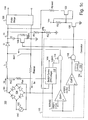
- FIGS. 1 a-c illustrates a schematic diagram of a power converter 100 in accordance with an aspect of the present invention.
- a power supply 102 such an AC power source, may provide a signal VAC that is coupled across input terminals of a bridge rectifier 104 .
- a first output terminal of the rectifier 104 may be coupled to a first terminal of an inductor L.
- a second terminal of the inductor L may be coupled to an anode of a rectifying diode D and to a first terminal of a switch SW 1 (e.g., a MOSFET).
- a cathode of the diode D may be coupled to a first terminal of a capacitor C.
- a second terminal of the capacitor C may be coupled to a first terminal of a resistor Rlimit.
- a second output terminal of the rectifier 104 may be coupled to a first terminal of a current-sensing resistor Rsense.
- a second terminal of the current-sensing resistor Rsense, a second terminal of the switch SW 1 and a second terminal of the resistor Rlimit may be coupled to a ground node.
- a transistor switch 106 may be coupled across the resistor Rlimit.
- the switch 106 Under normal operating conditions, the switch 106 is closed. When the switch SW 1 is closed, current from the rectifier 104 charges the inductor L with energy. When the switch SW 1 is opened, energy stored in the inductor L is discharged into the capacitor C. An output voltage Vo formed by the PFC stage across capacitor C may provide power to a load. As illustrated in FIGS. 1 a-c an exemplary load may be a pulse-width modulation (PWM) stage 108 of the converter 100 in which the output voltage Vo forms an input to the PWM stage 108 . A regulated output may be formed by the PWM stage 108 .
- PWM pulse-width modulation
- a controller 110 may control the switch SW 1 .
- a supply voltage Vcc may be used to provide power to circuitry of the controller 110 .
- the PWM stage 108 may form a supply voltage Vcc at its output. It will be apparent, however, that the supply voltage Vcc may be formed in another manner.
- the inductor L may serve as a primary winding of a transformer (not shown) such that current in the inductor L induces current in a secondary winding of the transformer. This induced current may then provide power to the controller 112 .
- a regulator (not shown) may be included in the controller 110 for supplying power to other circuitry of the controller 110 .
- the controller 110 controls the switch SW 1 so as to regulate an output voltage Vo formed at the first terminal of a capacitor C.
- the controller 110 may include a conventional PFC controller 112 which maintains the input current Iin substantially in phase with the input voltage VAC, in addition to regulating the output voltage Vo.
- the PFC controller 112 may receive a signal ISENSE formed at the first terminal of the sensing resistor Rsense that is representative of the input current Iin and a signal VFB that is representative of the output voltage Vo.
- the output voltage feedback signal VFB may be formed by applying the output voltage Vo to a first terminal of a resistor R 1 .
- a second terminal of the resistor R 1 may be coupled to a first terminal of a resistor R 2 .
- a second terminal of the resistor R 2 may be coupled to a ground node.
- the resistors R 1 and R 2 form a resistive divider.
- the signal VFB may be formed at the intermediate terminal of the resistive divider and coupled to the switch controller 112 .
- a first terminal of a resistor Rac may be coupled to a first output terminal of the rectifier 104 .
- a second terminal of the resistor Rac may be coupled to the switch controller 112 .
- a current IAC passes through the resistor Rac and, thus, forms a signal that is representative of the input voltage Vin. This signal may be used by the switch controller 112 to help ensure that the input current Iin follows the input voltage Vin.
- a signal VSW 1 formed by the PFC switch controller 112 controls the switch SW 1 by regulating its duty cycle.
- signal ISENSE is generally a negative voltage level since the current Iin causes a voltage drop across the resistor Rsense. In the event that the signal ISENSE exceeds (i.e. is more negative than) a first predetermined threshold, this indicates an excessive level of input current Iin. For example, this may occur if a load, such as the PWM stage 108 , draws an excessive current or experiences a fault. When this occurs, the switch SW 1 may be held open so as to limit the current Iin. To accomplish this, the signal ISENSE may be coupled to a first input of a comparator CMP 1 . A reference voltage VREF 1 (e.g., ⁇ 1.0 volts) may be coupled to a second input of the comparator CMP 1 .
- a reference voltage VREF 1 e.g., ⁇ 1.0 volts
- An output of the comparator CMP 1 may be coupled to a first input of a logic AND gate 114 .
- the output VSW 1 of the PFC switch controller 112 may be coupled to a second input of the logic AND gate 114 .
- An output of the logic AND gate 114 may be coupled to control the switch SW 1 .
- the output of the comparator CMP 1 is a logic high voltage. This allows the logic AND gate 114 to pass the signal VSW 1 such the switch SW 1 is opened and closed in accordance with the switch control signal VSW 1 .
- the output of the comparator CMP 1 is a logic low voltage. This prevents the logic AND gate 114 from passing the signal VSW 1 to the switch SW 1 . Accordingly, operation of the switch SW 1 halts.
- the signal ISENSE exceeds a second predetermined threshold, this indicates an even higher level of input current Iin than necessary to trigger the comparator CMP 1 .
- a large voltage may be applied across the inductor L, resulting in a large input current.
- This is also referred to as “inrush” current that occurs upon the application of VAC to the PFC stage prior to the output voltage Vo being developed to significant level.
- the switch 106 may be opened and the current-limiting resistor Rlimit coupled to receive the input current. As a result, the input current Iin is limited by the resistor Rlimit.
- the signal ISENSE may be coupled to a first input of a comparator CMP 2 .
- a reference voltage e.g., ⁇ 2.5 volts
- An output of the comparator CMP 2 may be coupled to control the switch 106 via a logic AND gate 116 . More particularly, the output of the comparator CMP 2 may be coupled to a first input of the logic AND gate 116 .
- An output of an under voltage lockout (UVLO) 118 may be coupled to a second (inverting) input of the logic AND gate 116 .
- An output of the logic AND gate 116 may be coupled to control the switch 106 .
- a bleed resistor Rbleed may provide current from the input supply VAC to power circuits of the controller 110 until the level of Vcc is sufficient to provide power to circuitry of the controller 110 .
- a first terminal of the bleed resistor Rbleed may be coupled to a terminal of the supply 102 , shown in FIG. 1 a , to an output terminal of the rectifier 104 , as shown in FIG. 1 b , or to the first terminal of the capacitor C, as shown in FIG. 1 c .
- a second terminal the resistor Rbleed may be coupled to provide power to the controller 110 via a transistor 122 .
- the output of the logic AND gate 116 may also be coupled to interrupt the current through the bleed resistor Rbleed.
- the UVLO 118 may have logic low voltage output until the level of Vcc rises to sufficient level (e.g., a predetermined level of 13 volts, where Vcc is nominally 15 volts) to operate circuits of the controller 110 .
- the output of the UVLO 118 may be combined with the output of the comparator CMP 1 by the AND gate 116 .
- the output of the logic AND gate 116 may be coupled to a gate of a transistor 120 .
- a source of the transistor 120 may be coupled to a ground node, while a drain of the transistor 120 may be coupled to a first terminal of a resistor R 3 and to a gate of a transistor 122 .
- the transistor switch 106 When the output of the AND gate 116 is a logic high voltage, the transistor switch 106 is open, while the transistor 120 is on (closed). As a result, the transistor 122 is closed. Thus, current passes through the bleed resistor Rbleed and the transistor 122 to provide power to the controller 110 .
- the output of the AND gate 116 changes to a logic low voltage.
- the switch 106 is closed, which shorts the resistor Rlimit, while the switch 122 is opened, which interrupts the current flowing through the bleed resistor Rbleed.
- power for the controller 110 may be provided by switching operation of the converter 100 , rather than by the bleed resistor Rbleed.
- the Vcc supply may be provided by current induced by current in the inductor L or by the output of the PWM stage of the controller 110 .
- the logic gate 116 performs the logic “AND” operation, the output of the comparator CMP 2 must be a logic high voltage and the output of the UVLO 118 must be a logic low voltage for the switch 106 to be opened and the switches 120 and 122 to be closed.
- the input current Iin must be exceed the predetermined threshold set by VREF 2 and the Vcc supply level must be below the predetermined threshold set by the UVLO for the input current Iin to be limited by the resistor Rlimit and for the current through the bleed resistor Rbleed to be enabled.
- the logic gate 116 may be configured to perform a logic “OR” operation. In that case, if the output of the comparator CMP 2 is a logic high voltage (indicating that the input current Iin exceeds the threshold set by VREF 2 ) or the output of the UVLO 118 is a logic low voltage (indicating the Vcc supply level is below the threshold set by the UVLO 118 ), then the input current Iin may be inhibited by the resistor Rlimit and the current through the bleed resistor Rbleed may be enabled.
- a single output of the controller 110 (e.g., at the output of the logic gate 116 ) may control both the shorting of the current-limiting resistor and removal of the bleed resistor. Accordingly, a single pin of an integrated circuit controller may control shorting of the current-limiting resistor and removal of the bleed resistor.
- FIGS. 2 a-c illustrate schematic diagrams of alternate embodiments of the power converter 100 of FIGS. 1 a-c in accordance with an aspect of the present invention.
- FIGS. 2 a-c differs from FIGS. 1 a-c in that the current-limiting resistor Rlimit is in parallel with the current-sensing resistor Rsense and the transistor 106 is in series with the resistor Rsense. When the transistor 106 is off, It acts as a diode clamp. As a result, most of the input current passes through the current-limiting resistor Rlimit. When the transistor 106 is on, most of the input current Iin passes through the current-sensing resistor Rsense. It will be apparent that other modifications may be made to the embodiments illustrated herein.
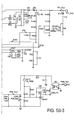
- FIG. 3 illustrates a schematic diagram of an exemplary controller 112 for the power converter of FIGS. 1 a-c or 2 a-c in accordance with an aspect of the present invention.
- the controller 112 uses average current-mode control to adjust the switching duty cycle of the switch SW 1 .
- the output voltage sensing signal VFB may be coupled to a first input of an amplifier 124 .
- a second input of the amplifier 124 may be coupled to receive a reference voltage VREF 3 .
- An output of the amplifier 124 forms an error signal which is representative of a difference between the output voltage Vo and a desired level for the output voltage Vo.
- the error signal may be coupled to a first input of a multiplier 126 .
- the input voltage sensing signal IAC may be coupled to a second input of the multiplier 126 .
- An output of the multiplier 126 may be coupled to a first input terminal of an amplifier 128 .
- the input current sensing signal ISENSE may be coupled to a second input of the amplifier 128 via a resistor R 4 .
- An output of the error amplifier 128 may be coupled to a first input terminal of a modulating comparator 130 .
- An oscillator 132 may form a clock signal VCLK and a linear periodic ramp signal VRAMP that is synchronized to the clock signal VCLK.
- the ramp signal VRAMP may be coupled to a second input terminal of the modulating comparator 130 .
- the ramp output of the oscillator 132 may be formed, for example, by charging a capacitor (not shown) with a constant current.
- An output of the modulating comparator 130 may be coupled as an input R of a flip-flop 134 .
- the clock output VCLK of the oscillator 132 may be coupled as an input S of the flip-flop 134 .
- An output Q of the flip-flop 134 may form the switch control signal VSW 1 .
- the signal output from the amplifier 128 modulates up and down. When compared to the linear ramp signal from the oscillator 132 , this adjusts the switching duty cycle. Thus, the amplifier 128 adjusts the switching duty cycle under closed loop control to maintain a voltage differential across its inputs to nearly zero volts. This forces the input current Iin to follow the waveform of the rectified sine wave of the input voltage Vin.
- the current control loop and the power delivery circuitry must have at least enough bandwidth to follow this waveform. It will be apparent that configuration of the controller 112 is exemplary and that modifications may be made.
- FIG. 4 illustrates a schematic diagram of an alternate embodiment of a controller 112 ′ for the power converter of FIGS. 1 a-c and 2 a-c in accordance with an aspect of the invention.
- the controller 112 ′ uses input current shaping to adjust the duty cycle of the switch SW 1 .
- the current sensing signal ISENSE is coupled to a first of a resistor R 5 .
- a second terminal of the resistor R 5 may be coupled to the first input of an amplifier 136 and to a first terminal of a resistor R 6 .
- a second terminal of the resistor R 6 may be coupled to the output of the amplifier 136 , while a second input of the amplifier 136 may be coupled to a ground node.
- a signal VA formed at the output of the amplifier 136 is representative of the input current Iin.
- the signal VA may be coupled to a first input of a comparator 138 .
- the voltage sensing signal VFB may be coupled to a first input terminal of an amplifier 140 .
- a second input terminal of the amplifier 140 may be coupled to receive a reference voltage VREF 4 .
- An output of the amplifier 140 forms an error signal VEAO which is representative of a difference between the output voltage Vo and a desired level for the output voltage Vo.
- a ramp generator 142 receives the error signal VEAO as an input and integrates the signal VEAO. Thus, the slope of a periodic ramp signal formed by the ramp generator 142 depends on the then-current level of the error signal VEAO.
- the signal from the ramp generator 142 is then applied to a squaring element 144 .
- An output of the squaring element is applied to the second input terminal of the comparator 138 .
- An output of the comparator 138 may be coupled to a set input S of a flip-flop or latch 146 .
- An oscillator 148 may form a clock signal VCLK, which is coupled to a reset input of the flip-flop 144 .
- a Q output of the flip-flop 146 may form the switch control signal VSW 1 which controls the duty cycle of the switch SW 1 and SW 2 .
- the signal VSW 1 may be reset to a logical low voltage level upon a leading edge of each pulse in the clock signal VCLK.
- the output of the comparator 138 may set the flip-flop 146 such that the switch control signal VSW 1 returns to a logical high voltage level.
- the duty cycle of the switch SW 1 is controlled with negative feedback to maintain the input current Iin in phase with the input voltage Vin and to regulate the output voltage Vo.
- leading or trailing edge modulation techniques may be utilized and that other types of modulation may be used, such as frequency modulation.
- the input voltage sensing signal IAC is not required. Accordingly, the resistor Rac may be omitted.
- FIGS. 5 a and 5 b illustrate a schematic diagram of a two-stage power factor correction and pulse width modulation power converter in accordance with an aspect of the present invention.
- An example of such a power converter is available under part number CM6900 from Champion Microelectronic Corporation, located at 4020 Moorpark Avenue, Suite 105, San Jose, Calif.
Abstract
A current inrush limiting technique for a switching power converter. In one aspect, a switching power converter includes a main power switch and a current sensor. When the input current exceeds a first threshold, the main power switch is opened. When the input current exceeds a second threshold, higher than the first threshold, a current-limiting resistance is coupled to receive the input current. Accordingly, the input current is limited in two stages by two different techniques. In another aspect, a bleed resistor receives current from a power source for providing power to a controller for the power converter. After start-up, such as when an output voltage of the power converter is available to provide power to the controller, the current-limiting resistor is shorted and the bleed resistor is effectively removed. A single pin of an integrated circuit controller controls shorting of the current-limiting resistor and removal of the bleed resistor.
Description
This application claims the benefit of U.S. Provisional Application Ser. No. 60/300,492, filed Jun. 21, 2001.
The present invention relates to switching power converters. More particularly, the present invention relates to limiting current inrush upon start-up of a switching power converter.
In a typical switching power converter, a duty cycle of a main power switch is controlled in response to a level of an output voltage developed by the power converter in order to regulate the output voltage. When power converter starts up, the output voltage is initially nearly zero. Accordingly, a large voltage may be applied across elements of the converter, resulting in a large inrush current. As a result, the current level may cause a circuit breaker that supplies power to the converter to trip or may cause damage to the converter itself.
A conventional technique for limiting the inrush current includes positioning a current-limiting resistor to receive the input current upon start-up and then shorting the resistor with a switch. Another technique includes placing a current-limiting resistor in parallel with a current-sensing resistor that is positioned to receive the input current. Upon start up, a switch in series with the sensing resistor directs the input current through the larger, current-limiting resistance. Then, the switch directs the input current through the sensing resistor.
A drawback to these techniques is that a dedicated pin would be required to implement them using an integrated circuit controller for the power converter.
In addition, in a conventional switching power converter, control circuitry, such as integrated circuit controller may obtain its operating power from an output of the power converter. During start-up, however, the output is not yet available. Thus, a bleed resistor is sometimes provided to obtain power from an input power source for the power converter, such as the AC supply.
A drawback to this technique is that during normal operation, the bleed resistor continues to draw power from the source, wasting energy. This is especially disadvantageous for devices for which a low energy consumption rating is desired.
An alternate technique involves shorting the bleed the resistor with a switch under normal operating conditions. However, this requires a dedicated pin to control the switch when the using an integrated circuit controller for the power converter.
Therefore, what is needed are improved techniques for preventing inrush current and for preventing power dissipation in a bleed resistor that do not suffer from the aforementioned drawbacks. It is to these ends that the present invention is directed.
The present invention is a current inrush limiting technique for a switching power converter. In one aspect of the invention, a switching power converter includes a main power switch and a current sensor, such as a sensing resistor, that forms a signal representative of an input current. When the input current exceeds a first threshold, the main power switch is opened. When the input current exceeds a second threshold, higher than the first threshold, a current-limiting resistance is coupled to receive the input current. Accordingly, the input current is limited in two stages by two different techniques.
In accordance with another aspect of the invention, a current sensor determines when a power converter is in a start-up mode. In response, a current-limiting resistor is coupled to receive the input current. In addition, a bleed resistor receives current from a power source for providing power to a controller for the power converter. After start-up, such as when an output voltage of the power converter is available to provide power to the controller, the current-limiting resistor is shorted and the bleed resistor is effectively removed. A single pin of an integrated circuit controller controls shorting of the current-limiting resistor and removal of the bleed resistor.
FIGS. 1a-c illustrate schematic diagrams of a power converter in accordance with an aspect of the present invention;
FIGS. 2a-c illustrate schematic diagrams of alternate embodiments of the power converter of FIGS. 1a-c in accordance with an aspect of the present invention;
FIG. 3 illustrates a schematic diagram of a controller for the power converter of FIGS. 1a-c or 2 a-c in accordance with an aspect of the present invention;
FIG. 4 illustrates a schematic diagram of an alternate embodiment of a controller for the power converter of FIGS. 1a-c or 2 a-c in accordance with an aspect of the present invention; and
FIGS. 5a and 5 b illustrate a schematic diagram of a two-stage power factor correction and pulse width modulation power converter in accordance with an aspect of the present invention.
FIGS. 1a-c illustrates a schematic diagram of a power converter 100 in accordance with an aspect of the present invention. A power supply 102, such an AC power source, may provide a signal VAC that is coupled across input terminals of a bridge rectifier 104. A first output terminal of the rectifier 104 may be coupled to a first terminal of an inductor L. A second terminal of the inductor L may be coupled to an anode of a rectifying diode D and to a first terminal of a switch SW1 (e.g., a MOSFET). A cathode of the diode D may be coupled to a first terminal of a capacitor C.
A second terminal of the capacitor C may be coupled to a first terminal of a resistor Rlimit. A second output terminal of the rectifier 104 may be coupled to a first terminal of a current-sensing resistor Rsense. A second terminal of the current-sensing resistor Rsense, a second terminal of the switch SW1 and a second terminal of the resistor Rlimit may be coupled to a ground node. A transistor switch 106 may be coupled across the resistor Rlimit. Collectively, the inductor L, switch SW1, diode D, and capacitor C form a power factor correction (PFC) stage of the power converter 100.
Under normal operating conditions, the switch 106 is closed. When the switch SW1 is closed, current from the rectifier 104 charges the inductor L with energy. When the switch SW1 is opened, energy stored in the inductor L is discharged into the capacitor C. An output voltage Vo formed by the PFC stage across capacitor C may provide power to a load. As illustrated in FIGS. 1a-c an exemplary load may be a pulse-width modulation (PWM) stage 108 of the converter 100 in which the output voltage Vo forms an input to the PWM stage 108. A regulated output may be formed by the PWM stage 108.
A controller 110, such as an integrated circuit controller, may control the switch SW1. As shown in FIGS. 1a-c a supply voltage Vcc may be used to provide power to circuitry of the controller 110. The PWM stage 108 may form a supply voltage Vcc at its output. It will be apparent, however, that the supply voltage Vcc may be formed in another manner. For example, the inductor L may serve as a primary winding of a transformer (not shown) such that current in the inductor L induces current in a secondary winding of the transformer. This induced current may then provide power to the controller 112. Further, a regulator (not shown) may be included in the controller 110 for supplying power to other circuitry of the controller 110.
The controller 110 controls the switch SW1 so as to regulate an output voltage Vo formed at the first terminal of a capacitor C. In one aspect, the controller 110 may include a conventional PFC controller 112 which maintains the input current Iin substantially in phase with the input voltage VAC, in addition to regulating the output voltage Vo. The PFC controller 112 may receive a signal ISENSE formed at the first terminal of the sensing resistor Rsense that is representative of the input current Iin and a signal VFB that is representative of the output voltage Vo.
The output voltage feedback signal VFB may be formed by applying the output voltage Vo to a first terminal of a resistor R1. A second terminal of the resistor R1 may be coupled to a first terminal of a resistor R2. A second terminal of the resistor R2 may be coupled to a ground node. Thus, the resistors R1 and R2 form a resistive divider. The signal VFB may be formed at the intermediate terminal of the resistive divider and coupled to the switch controller 112.
In addition, a first terminal of a resistor Rac may be coupled to a first output terminal of the rectifier 104. A second terminal of the resistor Rac may be coupled to the switch controller 112. A current IAC passes through the resistor Rac and, thus, forms a signal that is representative of the input voltage Vin. This signal may be used by the switch controller 112 to help ensure that the input current Iin follows the input voltage Vin. A signal VSW1 formed by the PFC switch controller 112 controls the switch SW1 by regulating its duty cycle.
Note that signal ISENSE is generally a negative voltage level since the current Iin causes a voltage drop across the resistor Rsense. In the event that the signal ISENSE exceeds (i.e. is more negative than) a first predetermined threshold, this indicates an excessive level of input current Iin. For example, this may occur if a load, such as the PWM stage 108, draws an excessive current or experiences a fault. When this occurs, the switch SW1 may be held open so as to limit the current Iin. To accomplish this, the signal ISENSE may be coupled to a first input of a comparator CMP1. A reference voltage VREF1 (e.g., −1.0 volts) may be coupled to a second input of the comparator CMP1. An output of the comparator CMP1 may be coupled to a first input of a logic AND gate 114. The output VSW1 of the PFC switch controller 112 may be coupled to a second input of the logic AND gate 114. An output of the logic AND gate 114 may be coupled to control the switch SW1.
Thus, when the level of ISENSE is higher than the level of VREF1, the output of the comparator CMP1 is a logic high voltage. This allows the logic AND gate 114 to pass the signal VSW1 such the switch SW1 is opened and closed in accordance with the switch control signal VSW1. However, when the input current Iin increases such that the level of ISENSE is lower than the level of REF1, the output of the comparator CMP1 is a logic low voltage. This prevents the logic AND gate 114 from passing the signal VSW1 to the switch SW1. Accordingly, operation of the switch SW1 halts.
In the event the signal ISENSE exceeds a second predetermined threshold, this indicates an even higher level of input current Iin than necessary to trigger the comparator CMP1. For example, during start-up when the output voltage Vo is zero or nearly zero, a large voltage may be applied across the inductor L, resulting in a large input current. This is also referred to as “inrush” current that occurs upon the application of VAC to the PFC stage prior to the output voltage Vo being developed to significant level. Under these conditions, the switch 106 may be opened and the current-limiting resistor Rlimit coupled to receive the input current. As a result, the input current Iin is limited by the resistor Rlimit.
To accomplish this current limiting, the signal ISENSE may be coupled to a first input of a comparator CMP2. A reference voltage (e.g., −2.5 volts) may be coupled to a second input of the comparator CMP2. An output of the comparator CMP2 may be coupled to control the switch 106 via a logic AND gate 116. More particularly, the output of the comparator CMP2 may be coupled to a first input of the logic AND gate 116. An output of an under voltage lockout (UVLO) 118 may be coupled to a second (inverting) input of the logic AND gate 116. An output of the logic AND gate 116 may be coupled to control the switch 106. Thus, when the output of the AND gate 116 is a logic high voltage, the switch 106 is opened, causing the input current Iin to generate a voltage across the resistor Rlimit, which tends to limit the input current Iin.
Also upon start-up, the level of the voltage Vcc may be too low to operate the controller 110 reliably. Accordingly, a bleed resistor Rbleed may provide current from the input supply VAC to power circuits of the controller 110 until the level of Vcc is sufficient to provide power to circuitry of the controller 110. A first terminal of the bleed resistor Rbleed may be coupled to a terminal of the supply 102, shown in FIG. 1a, to an output terminal of the rectifier 104, as shown in FIG. 1b, or to the first terminal of the capacitor C, as shown in FIG. 1c. A second terminal the resistor Rbleed may be coupled to provide power to the controller 110 via a transistor 122.
Once the level of Vcc is sufficient to provide power to the controller 100, the current through the bleed resistor Rbleed is no longer necessary. Rather, this current can contribute to inefficiency in the converter 100. Accordingly, in one embodiment of the invention, the output of the logic AND gate 116 may also be coupled to interrupt the current through the bleed resistor Rbleed.
More particularly, the UVLO 118 may have logic low voltage output until the level of Vcc rises to sufficient level (e.g., a predetermined level of 13 volts, where Vcc is nominally 15 volts) to operate circuits of the controller 110. Thus, the output of the UVLO 118 may be combined with the output of the comparator CMP1 by the AND gate 116. Also, the output of the logic AND gate 116 may be coupled to a gate of a transistor 120. A source of the transistor 120 may be coupled to a ground node, while a drain of the transistor 120 may be coupled to a first terminal of a resistor R3 and to a gate of a transistor 122. When the output of the AND gate 116 is a logic high voltage, the transistor switch 106 is open, while the transistor 120 is on (closed). As a result, the transistor 122 is closed. Thus, current passes through the bleed resistor Rbleed and the transistor 122 to provide power to the controller 110.
However, when the input current Iin is reduced such that the signal ISENSE causes the output of the comparator CMP2 to change to a logic low voltage and the supply voltage Vcc is reached the predetermined level, the output of the AND gate 116 changes to a logic low voltage. As a result, the switch 106 is closed, which shorts the resistor Rlimit, while the switch 122 is opened, which interrupts the current flowing through the bleed resistor Rbleed. Under these conditions, power for the controller 110 may be provided by switching operation of the converter 100, rather than by the bleed resistor Rbleed. For example, the Vcc supply may be provided by current induced by current in the inductor L or by the output of the PWM stage of the controller 110.
Note that because the logic gate 116 performs the logic “AND” operation, the output of the comparator CMP2 must be a logic high voltage and the output of the UVLO 118 must be a logic low voltage for the switch 106 to be opened and the switches 120 and 122 to be closed. In other words, the input current Iin must be exceed the predetermined threshold set by VREF2 and the Vcc supply level must be below the predetermined threshold set by the UVLO for the input current Iin to be limited by the resistor Rlimit and for the current through the bleed resistor Rbleed to be enabled.
Alternately, the logic gate 116 may be configured to perform a logic “OR” operation. In that case, if the output of the comparator CMP2 is a logic high voltage (indicating that the input current Iin exceeds the threshold set by VREF2) or the output of the UVLO 118 is a logic low voltage (indicating the Vcc supply level is below the threshold set by the UVLO 118), then the input current Iin may be inhibited by the resistor Rlimit and the current through the bleed resistor Rbleed may be enabled.
Thus, a single output of the controller 110 (e.g., at the output of the logic gate 116) may control both the shorting of the current-limiting resistor and removal of the bleed resistor. Accordingly, a single pin of an integrated circuit controller may control shorting of the current-limiting resistor and removal of the bleed resistor. An advantage of the invention is that the number of pins required of the controller is minimized.
FIGS. 2a-c illustrate schematic diagrams of alternate embodiments of the power converter 100 of FIGS. 1a-c in accordance with an aspect of the present invention. FIGS. 2a-c differs from FIGS. 1a-c in that the current-limiting resistor Rlimit is in parallel with the current-sensing resistor Rsense and the transistor 106 is in series with the resistor Rsense. When the transistor 106 is off, It acts as a diode clamp. As a result, most of the input current passes through the current-limiting resistor Rlimit. When the transistor 106 is on, most of the input current Iin passes through the current-sensing resistor Rsense. It will be apparent that other modifications may be made to the embodiments illustrated herein.
FIG. 3 illustrates a schematic diagram of an exemplary controller 112 for the power converter of FIGS. 1a-c or 2 a-c in accordance with an aspect of the present invention. The controller 112 uses average current-mode control to adjust the switching duty cycle of the switch SW1. The output voltage sensing signal VFB may be coupled to a first input of an amplifier 124. A second input of the amplifier 124 may be coupled to receive a reference voltage VREF3. An output of the amplifier 124 forms an error signal which is representative of a difference between the output voltage Vo and a desired level for the output voltage Vo. The error signal may be coupled to a first input of a multiplier 126. The input voltage sensing signal IAC may be coupled to a second input of the multiplier 126.
An output of the multiplier 126 may be coupled to a first input terminal of an amplifier 128. The input current sensing signal ISENSE may be coupled to a second input of the amplifier 128 via a resistor R4. An output of the error amplifier 128 may be coupled to a first input terminal of a modulating comparator 130. An oscillator 132 may form a clock signal VCLK and a linear periodic ramp signal VRAMP that is synchronized to the clock signal VCLK. The ramp signal VRAMP may be coupled to a second input terminal of the modulating comparator 130. The ramp output of the oscillator 132 may be formed, for example, by charging a capacitor (not shown) with a constant current. An output of the modulating comparator 130 may be coupled as an input R of a flip-flop 134. The clock output VCLK of the oscillator 132 may be coupled as an input S of the flip-flop 134. An output Q of the flip-flop 134 may form the switch control signal VSW1.
The signal output from the amplifier 128 modulates up and down. When compared to the linear ramp signal from the oscillator 132, this adjusts the switching duty cycle. Thus, the amplifier 128 adjusts the switching duty cycle under closed loop control to maintain a voltage differential across its inputs to nearly zero volts. This forces the input current Iin to follow the waveform of the rectified sine wave of the input voltage Vin. The current control loop and the power delivery circuitry must have at least enough bandwidth to follow this waveform. It will be apparent that configuration of the controller 112 is exemplary and that modifications may be made.
FIG. 4 illustrates a schematic diagram of an alternate embodiment of a controller 112′ for the power converter of FIGS. 1a-c and 2 a-c in accordance with an aspect of the invention. The controller 112′ uses input current shaping to adjust the duty cycle of the switch SW1. The current sensing signal ISENSE is coupled to a first of a resistor R5. A second terminal of the resistor R5 may be coupled to the first input of an amplifier 136 and to a first terminal of a resistor R6. A second terminal of the resistor R6 may be coupled to the output of the amplifier 136, while a second input of the amplifier 136 may be coupled to a ground node. A signal VA formed at the output of the amplifier 136 is representative of the input current Iin. The signal VA may be coupled to a first input of a comparator 138.
The voltage sensing signal VFB may be coupled to a first input terminal of an amplifier 140. A second input terminal of the amplifier 140 may be coupled to receive a reference voltage VREF4. An output of the amplifier 140 forms an error signal VEAO which is representative of a difference between the output voltage Vo and a desired level for the output voltage Vo.
A ramp generator 142 receives the error signal VEAO as an input and integrates the signal VEAO. Thus, the slope of a periodic ramp signal formed by the ramp generator 142 depends on the then-current level of the error signal VEAO. The signal from the ramp generator 142 is then applied to a squaring element 144. An output of the squaring element is applied to the second input terminal of the comparator 138.
An output of the comparator 138 may be coupled to a set input S of a flip-flop or latch 146. An oscillator 148 may form a clock signal VCLK, which is coupled to a reset input of the flip-flop 144. A Q output of the flip-flop 146 may form the switch control signal VSW1 which controls the duty cycle of the switch SW1 and SW2.
The signal VSW1 may be reset to a logical low voltage level upon a leading edge of each pulse in the clock signal VCLK. When the signal VC exceeds the signal VA, the output of the comparator 138 may set the flip-flop 146 such that the switch control signal VSW1 returns to a logical high voltage level. Thus, the duty cycle of the switch SW1 is controlled with negative feedback to maintain the input current Iin in phase with the input voltage Vin and to regulate the output voltage Vo. It will be apparent that leading or trailing edge modulation techniques may be utilized and that other types of modulation may be used, such as frequency modulation. Unlike the average current-mode controller illustrated in FIG. 3, the input voltage sensing signal IAC is not required. Accordingly, the resistor Rac may be omitted.
Other switching power supplies that perform power factor correction are described in: U.S. Pat. No. 5,804,950, entitled, “Input Current Modulation for Power Factor Correction;” U.S. Pat. No. 5,742,151, entitled, “Input Current Shaping Technique and Low Pin Count for PFC-PWM Boost Converter;” U.S. Pat. No. 5,798,635, entitled, “One Pin Error Amplifier and Switched Soft Start for an Eight Pin PFC-PWM Combination Integrated Circuit Converter Controller;” and co-pending U.S. patent application Ser. No. 10/159,142, filed May 31, 2002, and entitled, “Power Factor Correction with Carrier Control and Input Voltage Sensing” the contents of all of which are hereby incorporated by reference.
FIGS. 5a and 5 b illustrate a schematic diagram of a two-stage power factor correction and pulse width modulation power converter in accordance with an aspect of the present invention. An example of such a power converter is available under part number CM6900 from Champion Microelectronic Corporation, located at 4020 Moorpark Avenue, Suite 105, San Jose, Calif.
Thus, while the foregoing has been with reference to particular embodiments of the invention, it will be appreciated by those skilled in the art that changes in these embodiments may be made without departing from the principles and spirit of the invention, the scope of which is defined by the appended claims.
Claims (39)
1. A switching power converter comprising:
a switch for receiving an input current;
a current sensor for forming a signal representative of the input current; and
a controller for repeatedly opening and closing the switch for regulating an output voltage and when the input current exceeds a first threshold, operation of the main power switch is halted and when the input current exceeds a second threshold higher than the first threshold the input current is limited by a current-limiting resistance.
2. The power converter according to claim 1 , wherein the controller performs power factor correction.
3. The power converter according to claim 2 , wherein the controller power factor correction in accordance with average current-mode control.
4. The power converter according to claim 2 , wherein the controller performs power factor correction in accordance with input current shaping.
5. The power converter according to claim 1 , further comprising an output capacitor, wherein opening and closing the switch forms an output voltage across the output capacitor and wherein the current-limiting resistance is coupled in series with the output capacitor.
6. The power converter according to claim 5 , wherein the current limiting resistance is coupled between the output capacitor and a ground node.
7. The power converter according to claim 5 , further comprising a second switch coupled across the current-limiting resistance and when the input current does not exceed the second threshold, the second switch shorts the current-limiting resistance.
8. The power converter according to claim 1 , further comprising a source for generating the input current and wherein the current-limiting resistance is coupled to receive a return current to the source.
9. The power converter according to claim 8 , wherein the current-limiting resistance is coupled between a ground node and the source.
10. The power converter according to claim 8 , wherein the current sensor comprises a sensing resistor coupled to receive the return current to the source and when the input current exceeds the second threshold, a second switch inhibits current from flowing in the sensing resistor.
11. A switching power supply for drawing power from a source and for forming an output voltage, the switching power supply comprising:
a controller for controlling operation of a switch for modulating current from the source for forming the output voltage by alternately charging and discharging a reactive element;
a bleed resistor for supplying current to the controller;
a current-limiting resistor for limiting the current from the source; and
wherein the current supplied to the controller via the bleed resistor is inhibited and the current-limiting resistor is shorted in response to a single control signal.
12. The switching power supply according to claim 11 , wherein the current supplied to the controller via the bleed resistor is inhibited and the current-limiting resistor is shorted simultaneously.
13. The switching power supply according to claim 11 , wherein the controller comprises an integrated circuit controller and wherein the single control signal is formed at a pin of the integrated circuit controller.
14. The power converter according to claim 11 wherein during start-up, the controller receives power from the bleed resistor and, after start-up, the controller receives power from a voltage supply for the controller.
15. The power converter according to claim 11 , wherein the current-limiting resistor is shorted and the bleed current is through the bleed resistor is inhibited after the voltage supply exceeds a first predetermined voltage level and the input current is below a predetermined current level.
16. The power converter according to claim 11 wherein the current-limiting resistor is shorted and the bleed current through the bleed resistor is inhibited after either the voltage supply exceeds a first predetermined voltage level or the input current is below a predetermined current level.
17. The power converter according to claim 11 , wherein the controller performs power factor correction.
18. The power converter according to claim 17 , wherein the controller power factor correction in accordance with average current-mode control.
19. The power converter according to claim 17 , wherein the controller performs power factor correction in accordance with input current shaping.
20. The power converter according to claim 11 , further comprising an output capacitor, wherein opening and closing the switch forms an output voltage across the output capacitor and wherein the current-limiting resistance is coupled in series with the output capacitor.
21. The power converter according to claim 20 , wherein the current-limiting resistance is coupled between the output capacitor and a ground node.
22. The power converter according to claim 20 , further comprising a second switch coupled across the current-limiting resistance and when the input current does not exceed the second threshold, the second switch shorts the current-limiting resistance.
23. The power converter according to claim 11 , wherein the current-limiting resistance is coupled to receive a return current to the source.
24. The power converter according to claim 23 , wherein the current-limiting resistance is coupled between a ground node and the source.
25. The power converter according to claim 23 , further comprising a current sensor including a sensing resistor coupled to receive the return current to the source and when the input current exceeds a threshold, a second switch inhibits current from flowing in the sensing resistor.
26. A switching power supply for drawing power from a source and for forming an output switching power supply comprising:
a controller for controlling operation of a switch for modulating current from the source for forming the output voltage by alternately charging and discharging a reactive element;
a bleed resistor for supplying current to the controller;
a current-limiting resistor for limiting the current from the source; and
wherein the current supplied to the controller via the bleed resistor is inhibited and the current-limiting resistor is shorted simultaneously.
27. The switching power supply according to claim 26 , wherein the controller comprises an integrated circuit controller and wherein the current supplied to the controller via the bleed resistor is inhibited and the current-limiting resistor is shorted in response to a control signal formed at a single pin of the integrated circuit controller.
28. The power converter according to claim 26 , wherein during start-up, the controller receives power from the bleed resistor and, after start-up, the controller receives power from a voltage supply for the controller.
29. The power converter according to claim 26 , wherein the current-limiting resistor is shorted and the bleed current is through the bleed resistor is inhibited after the voltage supply exceeds a first predetermined voltage level and the input current is below a predetermined current level.
30. The power converter according to claim 26 , wherein the current-limiting resistor is shorted and the bleed current through the bleed resistor is inhibited after either the voltage supply exceeds a first predetermined voltage level or the input current is below a predetermined current level.
31. The power converter according to claim 26 , wherein the controller performs power factor correction.
32. The power converter according to claim 31 , wherein the controller performs power factor correction in accordance with average current-mode control.
33. The power converter according to claim 31 , wherein the controller performs power factor correction in accordance with input current shaping.
34. The power converter according to claim 26 , further comprising an output capacitor, wherein opening and closing the switch forms an output voltage across the output capacitor and wherein the current-limiting resistance is coupled in series with the output capacitor.
35. The power converter according to claim 34 , wherein the current-limiting resistance is coupled between the output capacitor and a ground node.
36. The power converter according to claim 34 , further comprising a second switch coupled across the current-limiting resistance and when the input current does not exceed the second threshold, the second switch shorts the current-limiting resistance.
37. The power converter according to claim 26 , wherein the current-limiting resistance is coupled to receive a return current to the source.
38. The power converter according to claim 37 , wherein the current-limiting resistance is coupled between a ground node and the source.
39. The power converter according to claim 37 , further comprising a current sensor including a sensing resistor coupled to receive the return current to the source and when the input current exceeds a threshold, a second switch inhibits current from flowing in the sensing resistor.
Priority Applications (1)
| Application Number | Priority Date | Filing Date | Title |
|---|---|---|---|
| US10/177,558 US6737845B2 (en) | 2001-06-21 | 2002-06-21 | Current inrush limiting and bleed resistor current inhibiting in a switching power converter |
Applications Claiming Priority (2)
| Application Number | Priority Date | Filing Date | Title |
|---|---|---|---|
| US30049201P | 2001-06-21 | 2001-06-21 | |
| US10/177,558 US6737845B2 (en) | 2001-06-21 | 2002-06-21 | Current inrush limiting and bleed resistor current inhibiting in a switching power converter |
Publications (2)
| Publication Number | Publication Date |
|---|---|
| US20020196644A1 US20020196644A1 (en) | 2002-12-26 |
| US6737845B2 true US6737845B2 (en) | 2004-05-18 |
Family
ID=23159323
Family Applications (3)
| Application Number | Title | Priority Date | Filing Date |
|---|---|---|---|
| US10/177,575 Abandoned US20020196006A1 (en) | 2001-06-21 | 2002-06-21 | Volt-second balanced PFCPWM power converter |
| US10/177,557 Expired - Fee Related US6674272B2 (en) | 2001-06-21 | 2002-06-21 | Current limiting technique for a switching power converter |
| US10/177,558 Expired - Fee Related US6737845B2 (en) | 2001-06-21 | 2002-06-21 | Current inrush limiting and bleed resistor current inhibiting in a switching power converter |
Family Applications Before (2)
| Application Number | Title | Priority Date | Filing Date |
|---|---|---|---|
| US10/177,575 Abandoned US20020196006A1 (en) | 2001-06-21 | 2002-06-21 | Volt-second balanced PFCPWM power converter |
| US10/177,557 Expired - Fee Related US6674272B2 (en) | 2001-06-21 | 2002-06-21 | Current limiting technique for a switching power converter |
Country Status (3)
| Country | Link |
|---|---|
| US (3) | US20020196006A1 (en) |
| AU (1) | AU2002322418A1 (en) |
| WO (2) | WO2003001315A1 (en) |
Cited By (70)
| Publication number | Priority date | Publication date | Assignee | Title |
|---|---|---|---|---|
| US20030218838A1 (en) * | 2002-05-22 | 2003-11-27 | Danfoss Drives A/S | Motor controller incorporating an electronic circuit for protection against inrush currents |
| US20050110469A1 (en) * | 2003-11-25 | 2005-05-26 | Sharp Kabushiki Kaisha | Power supply circuit |
| US20050231176A1 (en) * | 2004-04-20 | 2005-10-20 | Yu-Fen Liao | Conversion circuit for discriminating sourcing current and sinking current |
| US6969976B1 (en) * | 2003-11-07 | 2005-11-29 | National Semiconductor Corporation | Dynamic current limit adjustments |
| US6969977B1 (en) * | 2004-06-10 | 2005-11-29 | National Semiconductor Corporation | Soft-start voltage regulator circuit |
| US20060017424A1 (en) * | 2004-07-26 | 2006-01-26 | Intersil Americas Inc. | Current averaging circuit for a PWM power converter |
| US20060091872A1 (en) * | 2004-10-28 | 2006-05-04 | Tdk Corporation | Switching power supply control device and switching power supply |
| US20060273740A1 (en) * | 2005-06-07 | 2006-12-07 | Delta Electronics, Inc. | Parallel power supply with active droop current sharing circuit having current limiting function |
| US7196499B1 (en) * | 2005-09-27 | 2007-03-27 | 02Micro, Inc. | DC/DC converter with inductor current sensing capability |
| US20080143311A1 (en) * | 2006-12-14 | 2008-06-19 | Ta-Yung Yang | Method and circuit for providing compensations of current mode power converters |
| US20080198635A1 (en) * | 2007-02-21 | 2008-08-21 | Broadcom Corporation | Pulse width modulated ground/return for powered device |
| US20090016087A1 (en) * | 2007-07-09 | 2009-01-15 | Fuji Electric Device Technology Co., Ltd | Switching power source |
| US20090039851A1 (en) * | 2006-04-05 | 2009-02-12 | Sanyo Electric Co., Ltd. | Switching Control Circuit |
| US20090107149A1 (en) * | 2007-10-25 | 2009-04-30 | Honeywell International Inc. | Current-protected driver circuit for ignition exciter unit |
| US20090146620A1 (en) * | 2007-12-11 | 2009-06-11 | Primarion, Inc. | Methods and apparatus for current sensing |
| US20090190379A1 (en) * | 2008-01-30 | 2009-07-30 | John L Melanson | Switching regulator with boosted auxiliary winding supply |
| US20090190384A1 (en) * | 2008-01-30 | 2009-07-30 | Cirrus Logic, Inc. | Powering a power supply integrated circuit with sense current |
| US20090309633A1 (en) * | 2008-06-17 | 2009-12-17 | Monolithic Power Systems | Charge pump for switched capacitor circuits with slew-rate control of in-rush current |
| US20100013447A1 (en) * | 2008-07-17 | 2010-01-21 | Ricoh Company, Ltd., | Switching power supply circuit |
| US20100020579A1 (en) * | 2008-07-25 | 2010-01-28 | Melanson John L | Power Supply With Accurate Energy Measurement |
| US20100026270A1 (en) * | 2008-07-31 | 2010-02-04 | Eric Yang | Average input current limit method and apparatus thereof |
| US20100039099A1 (en) * | 2008-08-12 | 2010-02-18 | Hynix Semiconductor, Inc. | Power noise detecting device and power noise control device using the same |
| US20100060202A1 (en) * | 2007-03-12 | 2010-03-11 | Melanson John L | Lighting System with Lighting Dimmer Output Mapping |
| WO2010068223A1 (en) * | 2008-12-13 | 2010-06-17 | Hewlett-Packard Development Company, L.P. | Systems and methods for scaling a signal in a power factor correction circuit |
| US20100156319A1 (en) * | 2008-08-29 | 2010-06-24 | John Laurence Melanson | LED Lighting System with Accurate Current Control |
| US20100164631A1 (en) * | 2008-12-31 | 2010-07-01 | Cirrus Logic, Inc. | Electronic system having common mode voltage range enhancement |
| US20100171442A1 (en) * | 2008-12-12 | 2010-07-08 | Draper William A | Light Emitting Diode Based Lighting System With Time Division Ambient Light Feedback Response |
| US20100244726A1 (en) * | 2008-12-07 | 2010-09-30 | Melanson John L | Primary-side based control of secondary-side current for a transformer |
| US20100253305A1 (en) * | 2007-03-12 | 2010-10-07 | Melanson John L | Switching power converter control with spread spectrum based electromagnetic interference reduction |
| KR100992412B1 (en) | 2008-12-30 | 2010-11-05 | 주식회사 실리콘웍스 | Dc-dc converter |
| US20100308742A1 (en) * | 2007-03-12 | 2010-12-09 | Melanson John L | Power Control System for Current Regulated Light Sources |
| US20100327765A1 (en) * | 2009-06-30 | 2010-12-30 | Melanson John L | Low energy transfer mode for auxiliary power supply operation in a cascaded switching power converter |
| US20110006748A1 (en) * | 2009-07-10 | 2011-01-13 | Delta Electronics Inc. | System and method for limiting input-current surge in a switching mode power supply |
| US20110038185A1 (en) * | 2009-01-09 | 2011-02-17 | Swamy Mahesh M | Low stress soft charge circuit for diode front end variable frequency drive |
| US20110133711A1 (en) * | 2009-12-09 | 2011-06-09 | Rohm Co., Ltd. | Semiconductor device and switching regulator using the device |
| US7969125B2 (en) | 2007-05-02 | 2011-06-28 | Cirrus Logic, Inc. | Programmable power control system |
| US8018171B1 (en) | 2007-03-12 | 2011-09-13 | Cirrus Logic, Inc. | Multi-function duty cycle modifier |
| US8076920B1 (en) | 2007-03-12 | 2011-12-13 | Cirrus Logic, Inc. | Switching power converter and control system |
| US8102127B2 (en) | 2007-06-24 | 2012-01-24 | Cirrus Logic, Inc. | Hybrid gas discharge lamp-LED lighting system |
| US20120081081A1 (en) * | 2010-09-30 | 2012-04-05 | Intersil Americas Inc. | System and method for converting an ac input voltage to a regulated output current |
| US8179110B2 (en) | 2008-09-30 | 2012-05-15 | Cirrus Logic Inc. | Adjustable constant current source with continuous conduction mode (“CCM”) and discontinuous conduction mode (“DCM”) operation |
| US8198874B2 (en) | 2009-06-30 | 2012-06-12 | Cirrus Logic, Inc. | Switching power converter with current sensing transformer auxiliary power supply |
| US8212491B2 (en) | 2008-07-25 | 2012-07-03 | Cirrus Logic, Inc. | Switching power converter control with triac-based leading edge dimmer compatibility |
| US8222872B1 (en) | 2008-09-30 | 2012-07-17 | Cirrus Logic, Inc. | Switching power converter with selectable mode auxiliary power supply |
| US20120182662A1 (en) * | 2011-01-14 | 2012-07-19 | Himax Analogic, Inc. | Inrush Current Protection Circuit |
| US8248145B2 (en) | 2009-06-30 | 2012-08-21 | Cirrus Logic, Inc. | Cascode configured switching using at least one low breakdown voltage internal, integrated circuit switch to control at least one high breakdown voltage external switch |
| US20120229041A1 (en) * | 2009-11-05 | 2012-09-13 | Eldolab Holding B.V. | Led driver for powering an led unit from a electronic transformer |
| US8299722B2 (en) | 2008-12-12 | 2012-10-30 | Cirrus Logic, Inc. | Time division light output sensing and brightness adjustment for different spectra of light emitting diodes |
| US8344707B2 (en) | 2008-07-25 | 2013-01-01 | Cirrus Logic, Inc. | Current sensing in a switching power converter |
| US8482223B2 (en) | 2009-04-30 | 2013-07-09 | Cirrus Logic, Inc. | Calibration of lamps |
| US8482944B1 (en) * | 2010-10-29 | 2013-07-09 | Universal Lighting Technologies, Inc. | Electronic ballast with inrush protection circuit |
| US20130223120A1 (en) * | 2012-02-29 | 2013-08-29 | Murata Manufacturing Co., Ltd. | Method and apparatus for active inrush control of boost power stage |
| US8536799B1 (en) | 2010-07-30 | 2013-09-17 | Cirrus Logic, Inc. | Dimmer detection |
| US8569972B2 (en) | 2010-08-17 | 2013-10-29 | Cirrus Logic, Inc. | Dimmer output emulation |
| US8576589B2 (en) | 2008-01-30 | 2013-11-05 | Cirrus Logic, Inc. | Switch state controller with a sense current generated operating voltage |
| US8654483B2 (en) | 2009-11-09 | 2014-02-18 | Cirrus Logic, Inc. | Power system having voltage-based monitoring for over current protection |
| US8963535B1 (en) | 2009-06-30 | 2015-02-24 | Cirrus Logic, Inc. | Switch controlled current sensing using a hall effect sensor |
| US9155174B2 (en) | 2009-09-30 | 2015-10-06 | Cirrus Logic, Inc. | Phase control dimming compatible lighting systems |
| US9178415B1 (en) | 2009-10-15 | 2015-11-03 | Cirrus Logic, Inc. | Inductor over-current protection using a volt-second value representing an input voltage to a switching power converter |
| US20150340890A1 (en) * | 2014-05-21 | 2015-11-26 | Dialog Semiconductor Inc. | Power Supply with Fast Discharging for Configurable Output Voltage |
| US20160124029A1 (en) * | 2014-11-04 | 2016-05-05 | Stmicroelectronics S.R.L. | Detection circuit for an active discharge circuit of an x-capacitor, related active discharge circuit, integrated circuit and method |
| US20160336852A1 (en) * | 2015-05-15 | 2016-11-17 | On-Bright Electronics (Shanghai) Co., Ltd. | Systems and Methods for Output Current Regulation in Power Conversion Systems |
| US20170346413A1 (en) * | 2011-05-08 | 2017-11-30 | Paul Wilkinson Dent | Transformerless dc to ac converter |
| US9991802B2 (en) | 2014-04-18 | 2018-06-05 | On-Bright Electronics (Shanghai) Co., Ltd. | Systems and methods for regulating output currents of power conversion systems |
| US10003268B2 (en) | 2015-05-15 | 2018-06-19 | On-Bright Electronics (Shanghai) Co., Ltd. | Systems and methods for output current regulation in power conversion systems |
| US10170999B2 (en) | 2014-04-18 | 2019-01-01 | On-Bright Electronics (Shanghai) Co., Ltd. | Systems and methods for regulating output currents of power conversion systems |
| US10177665B2 (en) | 2013-07-19 | 2019-01-08 | On-Bright Electronics (Shanghai) Co., Ltd. | Systems and methods for high precision and/or low loss regulation of output currents of power conversion systems |
| US10211626B2 (en) | 2015-02-02 | 2019-02-19 | On-Bright Electronics (Shanghai) Co., Ltd. | System and method providing reliable over current protection for power converter |
| US10277110B2 (en) | 2010-12-08 | 2019-04-30 | On-Bright Electronics (Shanghai) Co., Ltd. | System and method providing over current protection based on duty cycle information for power converter |
| US10483869B1 (en) * | 2018-07-13 | 2019-11-19 | Stmicroelectronics Ltd | Power conversion circuit having inrush current limiting resistor bypass |
Families Citing this family (118)
| Publication number | Priority date | Publication date | Assignee | Title |
|---|---|---|---|---|
| AU2003233126A1 (en) * | 2002-06-04 | 2003-12-19 | Koninklijke Philips Electronics N.V. | Dc-dc converter |
| JP4010893B2 (en) * | 2002-07-08 | 2007-11-21 | ローム株式会社 | Stabilized power supply with current limiting function |
| JP4111109B2 (en) * | 2002-10-30 | 2008-07-02 | 株式会社デンソー | Switching regulator and power supply device |
| TW588489B (en) * | 2002-11-14 | 2004-05-21 | Richtek Technology Corp | Over-current protection apparatus and method of switching type regulator |
| US6922041B2 (en) * | 2003-02-28 | 2005-07-26 | Sipex Corporation | Apparatus for and method of adjusting a switching regulator output for a circuit having a pre-charge voltage |
| US7940033B2 (en) * | 2003-04-22 | 2011-05-10 | Aivaka, Inc. | Control loop for switching power converters |
| US6922346B2 (en) * | 2003-07-23 | 2005-07-26 | Texas Instruments Incorporated | System and method to limit maximum duty cycle and/or provide a maximum volt-second clamp |
| JP4271534B2 (en) * | 2003-09-01 | 2009-06-03 | 株式会社リコー | DC power supply device, driving method thereof, and semiconductor integrated circuit device including DC power supply circuit |
| JP2005086931A (en) * | 2003-09-10 | 2005-03-31 | Renesas Technology Corp | Switching power supply and semiconductor integrated circuit used for it |
| JP4356977B2 (en) * | 2003-12-04 | 2009-11-04 | キヤノン株式会社 | Power supply apparatus and recording apparatus provided with the power supply apparatus |
| ITMI20040486A1 (en) | 2004-03-16 | 2004-06-16 | St Microelectronics Srl | DEVICE FOR CORRECTION OF THE POWER FACTOR IN FORCED SWITCHING POWER SUPPLIES |
| US20050237037A1 (en) * | 2004-04-23 | 2005-10-27 | Intersil Americas Inc. | Switching power supply controller system and method |
| US7515393B2 (en) * | 2004-05-06 | 2009-04-07 | Hewlett-Packard Development Company, L.P. | Voltage regulator |
| US6969980B1 (en) * | 2004-05-21 | 2005-11-29 | Richtek Technology Corp. | Noise-resistant pulse width modulator |
| US7764057B2 (en) * | 2004-06-25 | 2010-07-27 | Intersil Americas Inc. | Constant-on-time switching power supply with virtual ripple feedback and related system and method |
| US6965223B1 (en) * | 2004-07-06 | 2005-11-15 | National Semiconductor Corporation | Method and apparatus to allow rapid adjustment of the reference voltage in a switching regulator |
| US7205752B2 (en) * | 2004-09-07 | 2007-04-17 | Flextronics Ap, Llc | Master-slave critical conduction mode power converter |
| US7638995B2 (en) * | 2005-01-18 | 2009-12-29 | Freescale Semiconductor, Inc. | Clocked ramp apparatus for voltage regulator softstart and method for softstarting voltage regulators |
| US7482794B2 (en) * | 2005-01-20 | 2009-01-27 | Board Of Regents, The University Of Texas System | System, method and apparatus for controlling converters using input-output linearization |
| US7646183B2 (en) * | 2005-05-31 | 2010-01-12 | Hewlett-Packard Development Company, L.P. | Adjusting an output voltage of a converter based on current consumption |
| US7522398B2 (en) * | 2005-07-06 | 2009-04-21 | Texas Instruments Incorporated | Method and apparatus for overcurrent protection in DC-DC power converters |
| US7378827B2 (en) * | 2005-08-24 | 2008-05-27 | Micrel, Incorporated | Analog internal soft-start and clamp circuit for switching regulator |
| US7737673B2 (en) * | 2005-09-30 | 2010-06-15 | Silicon Laboratories Inc. | Controlling a voltage regulator |
| US8954773B2 (en) | 2005-10-21 | 2015-02-10 | Freescale Semiconductor, Inc. | Electronic device and method for controlling current of a processor load by slewing clock frequency |
| US7265523B2 (en) * | 2005-10-24 | 2007-09-04 | Aivaka | Control loop for switching power converters |
| EP1801098A1 (en) | 2005-12-16 | 2007-06-27 | Merck Sante | 2-Adamantylurea derivatives as selective 11B-HSD1 inhibitors |
| US8558470B2 (en) * | 2006-01-20 | 2013-10-15 | Point Somee Limited Liability Company | Adaptive current regulation for solid state lighting |
| US8441210B2 (en) | 2006-01-20 | 2013-05-14 | Point Somee Limited Liability Company | Adaptive current regulation for solid state lighting |
| US8742674B2 (en) | 2006-01-20 | 2014-06-03 | Point Somee Limited Liability Company | Adaptive current regulation for solid state lighting |
| JP5420910B2 (en) * | 2006-02-14 | 2014-02-19 | フレクストロニクス エーピー,リミテッド ライアビリティ カンパニー | Power converter |
| WO2007127403A2 (en) * | 2006-04-26 | 2007-11-08 | Aivaka | Clock with regulated duty cycle and frequency |
| EP2020076A2 (en) * | 2006-04-27 | 2009-02-04 | Aivaka | Startup for dc/dc converters |
| EP2054787B1 (en) * | 2006-08-07 | 2009-12-23 | STMicroelectronics S.r.l. | Control device for power factor correction device in switching mode power supplies |
| WO2008039526A2 (en) * | 2006-09-25 | 2008-04-03 | Flextronics Ap, Llc | Bi-directional regulator |
| US8299771B2 (en) * | 2006-11-30 | 2012-10-30 | Infineon Technologies Ag | Methods and systems for driving a load |
| US7809408B2 (en) * | 2006-12-06 | 2010-10-05 | Broadcom Corporation | Method and system for a power switch with a slow in-rush current |
| EP1935420A1 (en) | 2006-12-21 | 2008-06-25 | Merck Sante | 2-Adamantyl-butyramide derivatives as selective 11beta-HSD1 inhibitors |
| EP2106675B1 (en) | 2007-01-22 | 2018-11-07 | Philips Intellectual Property & Standards GmbH | Organic light emitting diode arrangement |
| US8191241B2 (en) * | 2007-03-29 | 2012-06-05 | Flextronics Ap, Llc | Method of producing a multi-turn coil from folded flexible circuitry |
| US7830676B2 (en) * | 2007-03-29 | 2010-11-09 | Flextronics Ap, Llc | Primary only constant voltage/constant current (CVCC) control in quasi resonant convertor |
| US7755914B2 (en) * | 2007-03-29 | 2010-07-13 | Flextronics Ap, Llc | Pulse frequency to voltage conversion |
| US7760519B2 (en) * | 2007-03-29 | 2010-07-20 | Flextronics Ap, Llc | Primary only control quasi resonant convertor |
| GB2448741A (en) * | 2007-04-26 | 2008-10-29 | Cambridge Semiconductor Ltd | Current sensing and overload protection of a switch mode power converter |
| US7978489B1 (en) | 2007-08-03 | 2011-07-12 | Flextronics Ap, Llc | Integrated power converters |
| JP5151332B2 (en) * | 2007-09-11 | 2013-02-27 | 株式会社リコー | Synchronous rectification type switching regulator |
| WO2009042232A1 (en) * | 2007-09-25 | 2009-04-02 | Flextronics Ap, Llc | Thermally enhanced magnetic transformer |
| US7480157B1 (en) * | 2007-11-19 | 2009-01-20 | Zippy Technology Corp. | Power architecture for providing voltage modulation power |
| US8773086B1 (en) * | 2007-12-07 | 2014-07-08 | Marvell International Ltd. | Circuits and methods for dynamic voltage management |
| US8279646B1 (en) | 2007-12-14 | 2012-10-02 | Flextronics Ap, Llc | Coordinated power sequencing to limit inrush currents and ensure optimum filtering |
| ATE528841T1 (en) * | 2007-12-28 | 2011-10-15 | Siemens Ag | CIRCUIT ARRANGEMENT FOR EMC INTERFERENCE SUPPRESSION |
| AT506762B1 (en) * | 2008-04-15 | 2012-05-15 | Fachhochschule Technikum Wien | RULES FOR TWO-STAGE DC VOLTAGE CONVERTERS |
| EP2110374A1 (en) | 2008-04-18 | 2009-10-21 | Merck Sante | Benzofurane, benzothiophene, benzothiazol derivatives as FXR modulators |
| US7888917B2 (en) * | 2008-04-23 | 2011-02-15 | Honeywell International Inc. | Systems and methods for producing a substantially constant output voltage in a power source boost system |
| US8102678B2 (en) * | 2008-05-21 | 2012-01-24 | Flextronics Ap, Llc | High power factor isolated buck-type power factor correction converter |
| US8693213B2 (en) * | 2008-05-21 | 2014-04-08 | Flextronics Ap, Llc | Resonant power factor correction converter |
| US7987581B2 (en) * | 2008-05-28 | 2011-08-02 | Flextronics Ap, Llc | High power manufacturing friendly transformer |
| JP2009291006A (en) * | 2008-05-29 | 2009-12-10 | Fujitsu Ltd | Device and method for converting voltage, and program for determining duty ratio |
| WO2010032333A1 (en) * | 2008-09-22 | 2010-03-25 | 富士通株式会社 | Power control circuit, power supply unit, power supply system, and power controller control method |
| JP5093037B2 (en) * | 2008-10-03 | 2012-12-05 | サンケン電気株式会社 | Load drive circuit |
| TWI446670B (en) * | 2008-11-20 | 2014-07-21 | Richtek Technology Corp | Protection apparatus and method for boost converter |
| US8081019B2 (en) * | 2008-11-21 | 2011-12-20 | Flextronics Ap, Llc | Variable PFC and grid-tied bus voltage control |
| US8004260B2 (en) * | 2009-03-26 | 2011-08-23 | Delta Electronics, Inc. | Method and apparatus for multi-stage power supplies |
| US8040117B2 (en) * | 2009-05-15 | 2011-10-18 | Flextronics Ap, Llc | Closed loop negative feedback system with low frequency modulated gain |
| CN101562397B (en) * | 2009-05-27 | 2014-02-12 | 成都芯源系统有限公司 | Dual-mode constant current control method based on third winding detection and circuit thereof |
| US7986179B2 (en) * | 2009-06-12 | 2011-07-26 | Elite Semiconductor Memory Technology Inc. | Circuit and method for reducing popping sound |
| US8803498B2 (en) | 2009-06-18 | 2014-08-12 | Cirasys, Inc. | System, apparatus and methods for controlling multiple output converters |
| US9252683B2 (en) | 2009-06-18 | 2016-02-02 | Cirasys, Inc. | Tracking converters with input output linearization control |
| US9369041B2 (en) | 2009-06-18 | 2016-06-14 | Cirasys, Inc. | Analog input output linearization control |
| US8810221B2 (en) | 2009-06-18 | 2014-08-19 | The Board Of Regents, The University Of Texas System | System, method and apparatus for controlling converters using input-output linearization |
| US9690308B2 (en) | 2011-12-20 | 2017-06-27 | Board Of Regents, The University Of Texas System | System and method for controlling output ripple of DC-DC converters with leading edge modulation control using current injection |
| JP5486221B2 (en) * | 2009-06-23 | 2014-05-07 | スパンション エルエルシー | DC-DC converter control circuit, DC-DC converter and electronic apparatus |
| US8339055B2 (en) * | 2009-08-03 | 2012-12-25 | Intersil Americas Inc. | Inrush current limiter for an LED driver |
| JP2011067025A (en) * | 2009-09-17 | 2011-03-31 | Seiko Instruments Inc | Dc-dc converter |
| EP2501685A1 (en) | 2009-11-16 | 2012-09-26 | Mellitech | [1,5]-diazocin derivatives |
| US8937825B2 (en) * | 2009-12-10 | 2015-01-20 | Alfred E. Mann Foundation For Scientific Research | Timing controlled AC to DC converter |
| US8289741B2 (en) * | 2010-01-14 | 2012-10-16 | Flextronics Ap, Llc | Line switcher for power converters |
| DE102010006437B9 (en) * | 2010-02-01 | 2012-07-19 | Austriamicrosystems Ag | Voltage transformer arrangement and method for voltage conversion |
| US8586873B2 (en) * | 2010-02-23 | 2013-11-19 | Flextronics Ap, Llc | Test point design for a high speed bus |
| US8964413B2 (en) | 2010-04-22 | 2015-02-24 | Flextronics Ap, Llc | Two stage resonant converter enabling soft-switching in an isolated stage |
| US8488340B2 (en) | 2010-08-27 | 2013-07-16 | Flextronics Ap, Llc | Power converter with boost-buck-buck configuration utilizing an intermediate power regulating circuit |
| CN102064703B (en) * | 2010-11-04 | 2013-11-06 | 成都芯源系统有限公司 | Constant current output control device and method for switching power supply |
| US8928297B2 (en) * | 2011-01-31 | 2015-01-06 | Infineon Technologies Austria Ag | Ćuk based current source |
| WO2012148774A2 (en) * | 2011-04-25 | 2012-11-01 | Volterra Semiconductor Corporation | Integrated protection devices with monitoring of electrical characteristics |
| CN102255504B (en) * | 2011-07-04 | 2013-09-18 | 成都芯源系统有限公司 | Switch control circuit and method thereof |
| CN102290974B (en) * | 2011-08-18 | 2013-12-11 | 西安交通大学 | DAC (Digital-to-Analog Converter) technology based novel soft start circuit and soft start method thereof |
| KR101851930B1 (en) * | 2011-11-29 | 2018-04-26 | 삼성전자주식회사 | Ac-dc converter |
| US9042135B2 (en) * | 2012-02-03 | 2015-05-26 | Peregrine Semiconductor Corporation | Methods and apparatuses for a soft-start function with auto-disable |
| US9117991B1 (en) | 2012-02-10 | 2015-08-25 | Flextronics Ap, Llc | Use of flexible circuits incorporating a heat spreading layer and the rigidizing specific areas within such a construction by creating stiffening structures within said circuits by either folding, bending, forming or combinations thereof |
| KR101339575B1 (en) * | 2012-11-20 | 2014-02-12 | 삼성전기주식회사 | Multi output power supplying apparatus |
| US9862561B2 (en) | 2012-12-03 | 2018-01-09 | Flextronics Ap, Llc | Driving board folding machine and method of using a driving board folding machine to fold a flexible circuit |
| TWI472896B (en) | 2013-02-04 | 2015-02-11 | Asmedia Technology Inc | Voltage regulator circuit |
| US9490651B2 (en) | 2013-03-15 | 2016-11-08 | Flextronics Ap, Llc | Sweep frequency mode for magnetic resonant power transmission |
| US9338915B1 (en) | 2013-12-09 | 2016-05-10 | Flextronics Ap, Llc | Method of attaching electronic module on fabrics by stitching plated through holes |
| US9431896B2 (en) * | 2013-12-19 | 2016-08-30 | Texas Instruments Incorporated | Apparatus and method for zero voltage switching in bridgeless totem pole power factor correction converter |
| US9723713B1 (en) | 2014-05-16 | 2017-08-01 | Multek Technologies, Ltd. | Flexible printed circuit board hinge |
| US9549463B1 (en) | 2014-05-16 | 2017-01-17 | Multek Technologies, Ltd. | Rigid to flexible PC transition |
| US9621053B1 (en) * | 2014-08-05 | 2017-04-11 | Flextronics Ap, Llc | Peak power control technique for primary side controller operation in continuous conduction mode |
| JP6382020B2 (en) * | 2014-08-18 | 2018-08-29 | ローム株式会社 | Soft start circuit |
| US20160055578A1 (en) * | 2014-08-21 | 2016-02-25 | George Janas | System and method for monitoring student loan debt relief |
| US9793709B2 (en) * | 2014-09-25 | 2017-10-17 | The Boeing Company | Current drivers that utilize short circuit protection |
| US10154583B1 (en) | 2015-03-27 | 2018-12-11 | Flex Ltd | Mechanical strain reduction on flexible and rigid-flexible circuits |
| US9966840B2 (en) * | 2015-05-01 | 2018-05-08 | Champion Microelectronic Corporation | Switching power supply and improvements thereof |
| CN104953813B (en) * | 2015-06-26 | 2018-03-13 | 广东美的制冷设备有限公司 | The method and apparatus for preventing the output voltage overvoltage of PFC pfc circuit |
| DE102015223589A1 (en) * | 2015-11-27 | 2017-06-01 | Tridonic Gmbh & Co Kg | Switching converter with cyclic frequency change |
| EP3182572B1 (en) * | 2015-12-17 | 2019-11-13 | Grundfos Holding A/S | Electronic circuit and method for operating an electronic circuit |
| CN106982485B (en) * | 2016-01-15 | 2020-11-20 | 佛山市顺德区美的电热电器制造有限公司 | Electromagnetic heating equipment and low-loss control device and method for IGBT (insulated Gate Bipolar transistor) tube |
| JP2017131033A (en) * | 2016-01-20 | 2017-07-27 | 株式会社デンソー | Switching power supply device |
| JP2017129690A (en) * | 2016-01-20 | 2017-07-27 | ヤマハ株式会社 | Circuit and music instrument |
| GB201607622D0 (en) * | 2016-04-30 | 2016-06-15 | Powerventure Semiconductor Ltd | Switching converter |
| CN106849636B (en) * | 2017-04-13 | 2019-04-12 | 四川长虹电器股份有限公司 | Control circuit for Switching Power Supply |
| KR102579291B1 (en) * | 2018-02-07 | 2023-09-18 | 삼성전자주식회사 | Apparatus for Power Conversion and AC to DC Conversion |
| GB2582593B (en) * | 2019-03-26 | 2021-08-11 | Murata Manufacturing Co | Simple constant current limit for SEPIC or boost converter |
| EP3829043A1 (en) * | 2019-11-26 | 2021-06-02 | OSRAM GmbH | Electronic converter, corresponding lighting system and method of operating an electronic converter |
| GB202107505D0 (en) * | 2021-05-26 | 2021-07-07 | Nordic Semiconductor Asa | Control of analogue to digital converters |
| CN113922661A (en) * | 2021-09-28 | 2022-01-11 | 智新科技股份有限公司 | BOOST booster circuit and control method thereof |
| FR3131132A1 (en) * | 2021-12-21 | 2023-06-23 | Thales | STARTING CONTROL DEVICE FOR A PEAK CURRENT CONTROL CONVERTER. |
| CN114337299B (en) * | 2021-12-22 | 2023-09-15 | 上海杰瑞兆新信息科技有限公司 | Control system of secondary rectifying tube |
| KR102626216B1 (en) * | 2023-08-02 | 2024-01-17 | 주식회사 파두 | Inrush current limiting circuit for power system |
Citations (33)
| Publication number | Priority date | Publication date | Assignee | Title |
|---|---|---|---|---|
| US3646439A (en) | 1970-07-21 | 1972-02-29 | Gen Electric | Regulator with optical feedback arrangement wherein both input and output voltage are sensed |
| US4754388A (en) | 1985-07-15 | 1988-06-28 | Harris Corporation | Regulator circuit for converting alternating input to a constant direct output |
| US5010293A (en) | 1989-11-20 | 1991-04-23 | Raynet Corporation | Inrush current limiting circuit |
| US5012401A (en) | 1990-03-19 | 1991-04-30 | Allied-Signal Inc. | Switching power supply with foldback current limiting |
| US5396165A (en) | 1993-02-02 | 1995-03-07 | Teledyne Industries, Inc. | Efficient power transfer system |
| US5459652A (en) * | 1994-01-28 | 1995-10-17 | Compaq Computer Corp. | Boot strap circuit for power up control of power supplies |
| US5565761A (en) | 1994-09-02 | 1996-10-15 | Micro Linear Corp | Synchronous switching cascade connected offline PFC-PWM combination power converter controller |
| US5570276A (en) | 1993-11-15 | 1996-10-29 | Optimun Power Conversion, Inc. | Switching converter with open-loop input voltage regulation on primary side and closed-loop load regulation on secondary side |
| US5592128A (en) | 1995-03-30 | 1997-01-07 | Micro Linear Corporation | Oscillator for generating a varying amplitude feed forward PFC modulation ramp |
| US5742151A (en) | 1996-06-20 | 1998-04-21 | Micro Linear Corporation | Input current shaping technique and low pin count for pfc-pwm boost converter |
| US5747977A (en) | 1995-03-30 | 1998-05-05 | Micro Linear Corporation | Switching regulator having low power mode responsive to load power consumption |
| US5798635A (en) | 1996-06-20 | 1998-08-25 | Micro Linear Corporation | One pin error amplifier and switched soft-start for an eight pin PFC-PWM combination integrated circuit converter controller |
| US5804950A (en) | 1996-06-20 | 1998-09-08 | Micro Linear Corporation | Input current modulation for power factor correction |
| US5818207A (en) | 1996-12-11 | 1998-10-06 | Micro Linear Corporation | Three-pin buck converter and four-pin power amplifier having closed loop output voltage control |
| US5831418A (en) | 1996-12-03 | 1998-11-03 | Fujitsu Ltd. | Step-up/down DC-to-DC converter |
| US5859527A (en) | 1996-06-14 | 1999-01-12 | Skop Gmbh Ltd | Electrical signal supply with separate voltage and current control for an electrical load |
| US5894243A (en) | 1996-12-11 | 1999-04-13 | Micro Linear Corporation | Three-pin buck and four-pin boost converter having open loop output voltage control |
| US5903138A (en) | 1995-03-30 | 1999-05-11 | Micro Linear Corporation | Two-stage switching regulator having low power modes responsive to load power consumption |
| US5912552A (en) | 1997-02-12 | 1999-06-15 | Kabushiki Kaisha Toyoda Jidoshokki Seisakusho | DC to DC converter with high efficiency for light loads |
| US5912549A (en) | 1997-08-01 | 1999-06-15 | Lucent Technologies Inc. | Current mode controller for continuous conduction mode power factor correction circuit and method of operation thereof |
| US5914591A (en) | 1996-12-25 | 1999-06-22 | Matsushita Electric Industrial Co., Ltd. | Switching power supply |
| US5930130A (en) * | 1997-09-29 | 1999-07-27 | Jrs Technology, Inc. | Inrush protection circuit |
| US6060867A (en) | 1998-08-28 | 2000-05-09 | Lucent Technologies Inc. | Switch driver for a snubber circuit, method of operation thereof and power converter employing the same |
| US6091233A (en) | 1999-01-14 | 2000-07-18 | Micro Linear Corporation | Interleaved zero current switching in a power factor correction boost converter |
| US6140808A (en) | 1998-08-05 | 2000-10-31 | Intel Corporation | DC-to-DC converter with transient suppression |
| US6163712A (en) | 1998-02-04 | 2000-12-19 | Motorola, Inc. | Inrush current limiter with output voltage detection for control of input current level and activation of current bypass path |
| US6166528A (en) | 1999-11-02 | 2000-12-26 | Fairchild Semiconductor Corporation | Lossless current sensing in buck converters working with low duty cycles and high clock frequencies |
| US6215290B1 (en) | 1999-11-15 | 2001-04-10 | Semtech Corporation | Multi-phase and multi-module power supplies with balanced current between phases and modules |
| US6307356B1 (en) | 1998-06-18 | 2001-10-23 | Linear Technology Corporation | Voltage mode feedback burst mode circuit |
| US6346778B1 (en) | 1998-01-20 | 2002-02-12 | Bytecraft Pty Ltd | AC power converter |
| US6356468B1 (en) | 1998-10-05 | 2002-03-12 | Nokia Networks Oy | Arrangement for limiting starting current in a power supply |
| US6426885B1 (en) | 1999-10-06 | 2002-07-30 | Hitachi, Ltd. | Inverter device and motor driving device provided with inrush current prevention circuit |
| US6445165B1 (en) * | 2001-09-21 | 2002-09-03 | International Business Machines Corporation | Circuit for limiting inrush current to a power source |
Family Cites Families (3)
| Publication number | Priority date | Publication date | Assignee | Title |
|---|---|---|---|---|
| US5003454A (en) * | 1990-01-09 | 1991-03-26 | North American Philips Corporation | Power supply with improved power factor correction |
| US5540701A (en) * | 1994-05-20 | 1996-07-30 | Hugh Sharkey | Passive fixation anastomosis method and device |
| EP0951133A3 (en) * | 1998-04-15 | 2000-04-12 | HILTI Aktiengesellschaft | Method and active filter for reducing ripple of a current drawn by a charge from a network |
-
2002
- 2002-06-21 US US10/177,575 patent/US20020196006A1/en not_active Abandoned
- 2002-06-21 WO PCT/US2002/019712 patent/WO2003001315A1/en not_active Application Discontinuation
- 2002-06-21 WO PCT/US2002/021568 patent/WO2003000025A2/en not_active Application Discontinuation
- 2002-06-21 US US10/177,557 patent/US6674272B2/en not_active Expired - Fee Related
- 2002-06-21 US US10/177,558 patent/US6737845B2/en not_active Expired - Fee Related
- 2002-06-21 AU AU2002322418A patent/AU2002322418A1/en not_active Abandoned
Patent Citations (33)
| Publication number | Priority date | Publication date | Assignee | Title |
|---|---|---|---|---|
| US3646439A (en) | 1970-07-21 | 1972-02-29 | Gen Electric | Regulator with optical feedback arrangement wherein both input and output voltage are sensed |
| US4754388A (en) | 1985-07-15 | 1988-06-28 | Harris Corporation | Regulator circuit for converting alternating input to a constant direct output |
| US5010293A (en) | 1989-11-20 | 1991-04-23 | Raynet Corporation | Inrush current limiting circuit |
| US5012401A (en) | 1990-03-19 | 1991-04-30 | Allied-Signal Inc. | Switching power supply with foldback current limiting |
| US5396165A (en) | 1993-02-02 | 1995-03-07 | Teledyne Industries, Inc. | Efficient power transfer system |
| US5570276A (en) | 1993-11-15 | 1996-10-29 | Optimun Power Conversion, Inc. | Switching converter with open-loop input voltage regulation on primary side and closed-loop load regulation on secondary side |
| US5459652A (en) * | 1994-01-28 | 1995-10-17 | Compaq Computer Corp. | Boot strap circuit for power up control of power supplies |
| US5565761A (en) | 1994-09-02 | 1996-10-15 | Micro Linear Corp | Synchronous switching cascade connected offline PFC-PWM combination power converter controller |
| US5592128A (en) | 1995-03-30 | 1997-01-07 | Micro Linear Corporation | Oscillator for generating a varying amplitude feed forward PFC modulation ramp |
| US5747977A (en) | 1995-03-30 | 1998-05-05 | Micro Linear Corporation | Switching regulator having low power mode responsive to load power consumption |
| US5903138A (en) | 1995-03-30 | 1999-05-11 | Micro Linear Corporation | Two-stage switching regulator having low power modes responsive to load power consumption |
| US5859527A (en) | 1996-06-14 | 1999-01-12 | Skop Gmbh Ltd | Electrical signal supply with separate voltage and current control for an electrical load |
| US5742151A (en) | 1996-06-20 | 1998-04-21 | Micro Linear Corporation | Input current shaping technique and low pin count for pfc-pwm boost converter |
| US5798635A (en) | 1996-06-20 | 1998-08-25 | Micro Linear Corporation | One pin error amplifier and switched soft-start for an eight pin PFC-PWM combination integrated circuit converter controller |
| US5804950A (en) | 1996-06-20 | 1998-09-08 | Micro Linear Corporation | Input current modulation for power factor correction |
| US5831418A (en) | 1996-12-03 | 1998-11-03 | Fujitsu Ltd. | Step-up/down DC-to-DC converter |
| US5894243A (en) | 1996-12-11 | 1999-04-13 | Micro Linear Corporation | Three-pin buck and four-pin boost converter having open loop output voltage control |
| US5818207A (en) | 1996-12-11 | 1998-10-06 | Micro Linear Corporation | Three-pin buck converter and four-pin power amplifier having closed loop output voltage control |
| US5914591A (en) | 1996-12-25 | 1999-06-22 | Matsushita Electric Industrial Co., Ltd. | Switching power supply |
| US5912552A (en) | 1997-02-12 | 1999-06-15 | Kabushiki Kaisha Toyoda Jidoshokki Seisakusho | DC to DC converter with high efficiency for light loads |
| US5912549A (en) | 1997-08-01 | 1999-06-15 | Lucent Technologies Inc. | Current mode controller for continuous conduction mode power factor correction circuit and method of operation thereof |
| US5930130A (en) * | 1997-09-29 | 1999-07-27 | Jrs Technology, Inc. | Inrush protection circuit |
| US6346778B1 (en) | 1998-01-20 | 2002-02-12 | Bytecraft Pty Ltd | AC power converter |
| US6163712A (en) | 1998-02-04 | 2000-12-19 | Motorola, Inc. | Inrush current limiter with output voltage detection for control of input current level and activation of current bypass path |
| US6307356B1 (en) | 1998-06-18 | 2001-10-23 | Linear Technology Corporation | Voltage mode feedback burst mode circuit |
| US6140808A (en) | 1998-08-05 | 2000-10-31 | Intel Corporation | DC-to-DC converter with transient suppression |
| US6060867A (en) | 1998-08-28 | 2000-05-09 | Lucent Technologies Inc. | Switch driver for a snubber circuit, method of operation thereof and power converter employing the same |
| US6356468B1 (en) | 1998-10-05 | 2002-03-12 | Nokia Networks Oy | Arrangement for limiting starting current in a power supply |
| US6091233A (en) | 1999-01-14 | 2000-07-18 | Micro Linear Corporation | Interleaved zero current switching in a power factor correction boost converter |
| US6426885B1 (en) | 1999-10-06 | 2002-07-30 | Hitachi, Ltd. | Inverter device and motor driving device provided with inrush current prevention circuit |
| US6166528A (en) | 1999-11-02 | 2000-12-26 | Fairchild Semiconductor Corporation | Lossless current sensing in buck converters working with low duty cycles and high clock frequencies |
| US6215290B1 (en) | 1999-11-15 | 2001-04-10 | Semtech Corporation | Multi-phase and multi-module power supplies with balanced current between phases and modules |
| US6445165B1 (en) * | 2001-09-21 | 2002-09-03 | International Business Machines Corporation | Circuit for limiting inrush current to a power source |
Cited By (143)
| Publication number | Priority date | Publication date | Assignee | Title |
|---|---|---|---|---|
| US7050278B2 (en) * | 2002-05-22 | 2006-05-23 | Danfoss Drives A/S | Motor controller incorporating an electronic circuit for protection against inrush currents |
| US20030218838A1 (en) * | 2002-05-22 | 2003-11-27 | Danfoss Drives A/S | Motor controller incorporating an electronic circuit for protection against inrush currents |
| US6969976B1 (en) * | 2003-11-07 | 2005-11-29 | National Semiconductor Corporation | Dynamic current limit adjustments |
| US20050110469A1 (en) * | 2003-11-25 | 2005-05-26 | Sharp Kabushiki Kaisha | Power supply circuit |
| US7129679B2 (en) * | 2003-11-25 | 2006-10-31 | Sharp Kabushiki Kaisha | Power supply circuit having soft start |
| US20050231176A1 (en) * | 2004-04-20 | 2005-10-20 | Yu-Fen Liao | Conversion circuit for discriminating sourcing current and sinking current |
| US6960902B1 (en) * | 2004-04-20 | 2005-11-01 | Richtek Technology Corp. | Conversion circuit for discriminating sourcing current and sinking current |
| US6969977B1 (en) * | 2004-06-10 | 2005-11-29 | National Semiconductor Corporation | Soft-start voltage regulator circuit |
| US7196503B2 (en) * | 2004-07-26 | 2007-03-27 | Intersil Americas, Inc. | Current averaging circuit for a PWM power converter |
| US20060017424A1 (en) * | 2004-07-26 | 2006-01-26 | Intersil Americas Inc. | Current averaging circuit for a PWM power converter |
| US20060091872A1 (en) * | 2004-10-28 | 2006-05-04 | Tdk Corporation | Switching power supply control device and switching power supply |
| US7132818B2 (en) * | 2004-10-28 | 2006-11-07 | Tdk Corporation | Switching power supply control device and switching power supply |
| US7541793B2 (en) * | 2005-06-07 | 2009-06-02 | Delta Electronics, Inc. | Parallel power supply with active droop current sharing circuit having current limiting function |
| US20060273740A1 (en) * | 2005-06-07 | 2006-12-07 | Delta Electronics, Inc. | Parallel power supply with active droop current sharing circuit having current limiting function |
| US20070069699A1 (en) * | 2005-09-27 | 2007-03-29 | Laszlo Lipcsei | Dc/dc converter with inductor current sensing capability |
| US7196499B1 (en) * | 2005-09-27 | 2007-03-27 | 02Micro, Inc. | DC/DC converter with inductor current sensing capability |
| US7782024B2 (en) * | 2006-04-05 | 2010-08-24 | Sanyo Electric Co., Ltd. | Switching control circuit |
| US20090039851A1 (en) * | 2006-04-05 | 2009-02-12 | Sanyo Electric Co., Ltd. | Switching Control Circuit |
| TWI407673B (en) * | 2006-04-05 | 2013-09-01 | Sanyo Electric Co | Switch control circuit |
| US7800927B2 (en) * | 2006-12-14 | 2010-09-21 | System General Corp. | Method and circuit for providing compensations of current mode power converters |
| US20080143311A1 (en) * | 2006-12-14 | 2008-06-19 | Ta-Yung Yang | Method and circuit for providing compensations of current mode power converters |
| US20080198635A1 (en) * | 2007-02-21 | 2008-08-21 | Broadcom Corporation | Pulse width modulated ground/return for powered device |
| US20100308742A1 (en) * | 2007-03-12 | 2010-12-09 | Melanson John L | Power Control System for Current Regulated Light Sources |
| US8174204B2 (en) | 2007-03-12 | 2012-05-08 | Cirrus Logic, Inc. | Lighting system with power factor correction control data determined from a phase modulated signal |
| US8232736B2 (en) | 2007-03-12 | 2012-07-31 | Cirrus Logic, Inc. | Power control system for current regulated light sources |
| US8018171B1 (en) | 2007-03-12 | 2011-09-13 | Cirrus Logic, Inc. | Multi-function duty cycle modifier |
| US8536794B2 (en) | 2007-03-12 | 2013-09-17 | Cirrus Logic, Inc. | Lighting system with lighting dimmer output mapping |
| US20100253305A1 (en) * | 2007-03-12 | 2010-10-07 | Melanson John L | Switching power converter control with spread spectrum based electromagnetic interference reduction |
| US8076920B1 (en) | 2007-03-12 | 2011-12-13 | Cirrus Logic, Inc. | Switching power converter and control system |
| US8723438B2 (en) | 2007-03-12 | 2014-05-13 | Cirrus Logic, Inc. | Switch power converter control with spread spectrum based electromagnetic interference reduction |
| US20100060202A1 (en) * | 2007-03-12 | 2010-03-11 | Melanson John L | Lighting System with Lighting Dimmer Output Mapping |
| US7969125B2 (en) | 2007-05-02 | 2011-06-28 | Cirrus Logic, Inc. | Programmable power control system |
| US8040703B2 (en) | 2007-05-02 | 2011-10-18 | Cirrus Logic, Inc. | Power factor correction controller with feedback reduction |
| US8120341B2 (en) | 2007-05-02 | 2012-02-21 | Cirrus Logic, Inc. | Switching power converter with switch control pulse width variability at low power demand levels |
| US8125805B1 (en) | 2007-05-02 | 2012-02-28 | Cirrus Logic Inc. | Switch-mode converter operating in a hybrid discontinuous conduction mode (DCM)/continuous conduction mode (CCM) that uses double or more pulses in a switching period |
| US8102127B2 (en) | 2007-06-24 | 2012-01-24 | Cirrus Logic, Inc. | Hybrid gas discharge lamp-LED lighting system |
| US7936152B2 (en) * | 2007-07-09 | 2011-05-03 | Fuji Electric Systems Co., Ltd. | Switching power source |
| US20090016087A1 (en) * | 2007-07-09 | 2009-01-15 | Fuji Electric Device Technology Co., Ltd | Switching power source |
| US8027142B2 (en) | 2007-10-25 | 2011-09-27 | Honeywell International Inc. | Current-protected driver circuit for ignition exciter unit |
| US20090107149A1 (en) * | 2007-10-25 | 2009-04-30 | Honeywell International Inc. | Current-protected driver circuit for ignition exciter unit |
| US8143870B2 (en) * | 2007-12-11 | 2012-03-27 | Ng Timothy M | Methods and apparatus for current sensing |
| US20090146620A1 (en) * | 2007-12-11 | 2009-06-11 | Primarion, Inc. | Methods and apparatus for current sensing |
| US8576589B2 (en) | 2008-01-30 | 2013-11-05 | Cirrus Logic, Inc. | Switch state controller with a sense current generated operating voltage |
| US8008898B2 (en) | 2008-01-30 | 2011-08-30 | Cirrus Logic, Inc. | Switching regulator with boosted auxiliary winding supply |
| US20090190379A1 (en) * | 2008-01-30 | 2009-07-30 | John L Melanson | Switching regulator with boosted auxiliary winding supply |
| US20090190384A1 (en) * | 2008-01-30 | 2009-07-30 | Cirrus Logic, Inc. | Powering a power supply integrated circuit with sense current |
| US8022683B2 (en) * | 2008-01-30 | 2011-09-20 | Cirrus Logic, Inc. | Powering a power supply integrated circuit with sense current |
| US20090309633A1 (en) * | 2008-06-17 | 2009-12-17 | Monolithic Power Systems | Charge pump for switched capacitor circuits with slew-rate control of in-rush current |
| US8049551B2 (en) | 2008-06-17 | 2011-11-01 | Monolithic Power Systems, Inc. | Charge pump for switched capacitor circuits with slew-rate control of in-rush current |
| US7884584B2 (en) * | 2008-07-17 | 2011-02-08 | Ricoh Company, Ltd. | Switching power supply circuit |
| US20100013447A1 (en) * | 2008-07-17 | 2010-01-21 | Ricoh Company, Ltd., | Switching power supply circuit |
| US8344707B2 (en) | 2008-07-25 | 2013-01-01 | Cirrus Logic, Inc. | Current sensing in a switching power converter |
| US20100020573A1 (en) * | 2008-07-25 | 2010-01-28 | Melanson John L | Audible noise suppression in a resonant switching power converter |
| US8014176B2 (en) | 2008-07-25 | 2011-09-06 | Cirrus Logic, Inc. | Resonant switching power converter with burst mode transition shaping |
| US8212491B2 (en) | 2008-07-25 | 2012-07-03 | Cirrus Logic, Inc. | Switching power converter control with triac-based leading edge dimmer compatibility |
| US8279628B2 (en) | 2008-07-25 | 2012-10-02 | Cirrus Logic, Inc. | Audible noise suppression in a resonant switching power converter |
| US8330434B2 (en) | 2008-07-25 | 2012-12-11 | Cirrus Logic, Inc. | Power supply that determines energy consumption and outputs a signal indicative of energy consumption |
| US20100020579A1 (en) * | 2008-07-25 | 2010-01-28 | Melanson John L | Power Supply With Accurate Energy Measurement |
| US20100020569A1 (en) * | 2008-07-25 | 2010-01-28 | Melanson John L | Resonant switching power converter with adaptive dead time control |
| US8553430B2 (en) | 2008-07-25 | 2013-10-08 | Cirrus Logic, Inc. | Resonant switching power converter with adaptive dead time control |
| US20100020570A1 (en) * | 2008-07-25 | 2010-01-28 | Melanson John L | Resonant switching power converter with burst mode transition shaping |
| US20100026270A1 (en) * | 2008-07-31 | 2010-02-04 | Eric Yang | Average input current limit method and apparatus thereof |
| US7952364B2 (en) * | 2008-08-12 | 2011-05-31 | Hynix Semiconductor Inc. | Power noise detecting device and power noise control device using the same |
| US20100039099A1 (en) * | 2008-08-12 | 2010-02-18 | Hynix Semiconductor, Inc. | Power noise detecting device and power noise control device using the same |
| US20100156319A1 (en) * | 2008-08-29 | 2010-06-24 | John Laurence Melanson | LED Lighting System with Accurate Current Control |
| US8487546B2 (en) | 2008-08-29 | 2013-07-16 | Cirrus Logic, Inc. | LED lighting system with accurate current control |
| US8222872B1 (en) | 2008-09-30 | 2012-07-17 | Cirrus Logic, Inc. | Switching power converter with selectable mode auxiliary power supply |
| US8179110B2 (en) | 2008-09-30 | 2012-05-15 | Cirrus Logic Inc. | Adjustable constant current source with continuous conduction mode (“CCM”) and discontinuous conduction mode (“DCM”) operation |
| US8288954B2 (en) | 2008-12-07 | 2012-10-16 | Cirrus Logic, Inc. | Primary-side based control of secondary-side current for a transformer |
| US20100244726A1 (en) * | 2008-12-07 | 2010-09-30 | Melanson John L | Primary-side based control of secondary-side current for a transformer |
| US20100171442A1 (en) * | 2008-12-12 | 2010-07-08 | Draper William A | Light Emitting Diode Based Lighting System With Time Division Ambient Light Feedback Response |
| US8299722B2 (en) | 2008-12-12 | 2012-10-30 | Cirrus Logic, Inc. | Time division light output sensing and brightness adjustment for different spectra of light emitting diodes |
| US8362707B2 (en) | 2008-12-12 | 2013-01-29 | Cirrus Logic, Inc. | Light emitting diode based lighting system with time division ambient light feedback response |
| WO2010068223A1 (en) * | 2008-12-13 | 2010-06-17 | Hewlett-Packard Development Company, L.P. | Systems and methods for scaling a signal in a power factor correction circuit |
| US8564269B2 (en) | 2008-12-13 | 2013-10-22 | Hewlett-Packard Development Company, L.P. | Systems and methods for scaling a signal in a power factor correction circuit |
| US20110235372A1 (en) * | 2008-12-13 | 2011-09-29 | David Paul Mohr | Systems And Methods For Scaling A Signal In A Power Factor Correction Circuit |
| KR100992412B1 (en) | 2008-12-30 | 2010-11-05 | 주식회사 실리콘웍스 | Dc-dc converter |
| US20100164631A1 (en) * | 2008-12-31 | 2010-07-01 | Cirrus Logic, Inc. | Electronic system having common mode voltage range enhancement |
| US7994863B2 (en) | 2008-12-31 | 2011-08-09 | Cirrus Logic, Inc. | Electronic system having common mode voltage range enhancement |
| US8274803B2 (en) * | 2009-01-09 | 2012-09-25 | Yaskawa America, Inc. | Low stress soft charge circuit for diode front end variable frequency drive |
| US20110038185A1 (en) * | 2009-01-09 | 2011-02-17 | Swamy Mahesh M | Low stress soft charge circuit for diode front end variable frequency drive |
| US8482223B2 (en) | 2009-04-30 | 2013-07-09 | Cirrus Logic, Inc. | Calibration of lamps |
| US20100327765A1 (en) * | 2009-06-30 | 2010-12-30 | Melanson John L | Low energy transfer mode for auxiliary power supply operation in a cascaded switching power converter |
| US8212493B2 (en) | 2009-06-30 | 2012-07-03 | Cirrus Logic, Inc. | Low energy transfer mode for auxiliary power supply operation in a cascaded switching power converter |
| US8963535B1 (en) | 2009-06-30 | 2015-02-24 | Cirrus Logic, Inc. | Switch controlled current sensing using a hall effect sensor |
| US8248145B2 (en) | 2009-06-30 | 2012-08-21 | Cirrus Logic, Inc. | Cascode configured switching using at least one low breakdown voltage internal, integrated circuit switch to control at least one high breakdown voltage external switch |
| US8198874B2 (en) | 2009-06-30 | 2012-06-12 | Cirrus Logic, Inc. | Switching power converter with current sensing transformer auxiliary power supply |
| US20110006748A1 (en) * | 2009-07-10 | 2011-01-13 | Delta Electronics Inc. | System and method for limiting input-current surge in a switching mode power supply |
| US8299773B2 (en) * | 2009-07-10 | 2012-10-30 | Delta Electronics, Inc. | System and method for limiting input-current surge in a switching mode power supply |
| US9155174B2 (en) | 2009-09-30 | 2015-10-06 | Cirrus Logic, Inc. | Phase control dimming compatible lighting systems |
| US9178415B1 (en) | 2009-10-15 | 2015-11-03 | Cirrus Logic, Inc. | Inductor over-current protection using a volt-second value representing an input voltage to a switching power converter |
| US20120229041A1 (en) * | 2009-11-05 | 2012-09-13 | Eldolab Holding B.V. | Led driver for powering an led unit from a electronic transformer |
| US9301348B2 (en) * | 2009-11-05 | 2016-03-29 | Eldolab Holding B.V. | LED driver for powering an LED unit from a electronic transformer |
| US9936551B2 (en) | 2009-11-05 | 2018-04-03 | Eldolab Holding B.V. | LED driver for powering an LED unit from an electronic transformer |
| US8654483B2 (en) | 2009-11-09 | 2014-02-18 | Cirrus Logic, Inc. | Power system having voltage-based monitoring for over current protection |
| US8582259B2 (en) * | 2009-12-09 | 2013-11-12 | Rohm Co., Ltd. | Semiconductor device and switching regulator using the device |
| US8964343B2 (en) | 2009-12-09 | 2015-02-24 | Rohm Co., Ltd. | Semiconductor device and switching regulator using the device |
| US20110133711A1 (en) * | 2009-12-09 | 2011-06-09 | Rohm Co., Ltd. | Semiconductor device and switching regulator using the device |
| US8536799B1 (en) | 2010-07-30 | 2013-09-17 | Cirrus Logic, Inc. | Dimmer detection |
| US8569972B2 (en) | 2010-08-17 | 2013-10-29 | Cirrus Logic, Inc. | Dimmer output emulation |
| US8754625B2 (en) * | 2010-09-30 | 2014-06-17 | Intersil Americas Inc. | System and method for converting an AC input voltage to regulated output current |
| US20120081081A1 (en) * | 2010-09-30 | 2012-04-05 | Intersil Americas Inc. | System and method for converting an ac input voltage to a regulated output current |
| TWI475794B (en) * | 2010-09-30 | 2015-03-01 | Intersil Inc | Converter, electronic device and method for converting an ac input voltage to a regulated output current |
| US8482944B1 (en) * | 2010-10-29 | 2013-07-09 | Universal Lighting Technologies, Inc. | Electronic ballast with inrush protection circuit |
| US11114933B2 (en) | 2010-12-08 | 2021-09-07 | On-Bright Electronics (Shanghai) Co., Ltd. | System and method providing over current protection based on duty cycle information for power converter |
| US10811955B2 (en) | 2010-12-08 | 2020-10-20 | On-Bright Electronics (Shanghai) Co., Ltd. | System and method providing over current protection based on duty cycle information for power converter |
| US10581315B2 (en) | 2010-12-08 | 2020-03-03 | On-Bright Electronics (Shanghai) Co., Ltd. | System and method providing over current protection based on duty cycle information for power converter |
| US11264888B2 (en) | 2010-12-08 | 2022-03-01 | On-Bright Electronics (Shanghai) Co., Ltd. | System and method providing over current protection based on duty cycle information for power converter |
| US10483838B2 (en) | 2010-12-08 | 2019-11-19 | On-Bright Electronics (Shanghai) Co., Ltd. | System and method providing over current protection based on duty cycle information for power converter |
| US10615684B2 (en) | 2010-12-08 | 2020-04-07 | On-Bright Electronics (Shanghai) Co., Ltd. | System and method providing over current protection based on duty cycle information for power converter |
| US10277110B2 (en) | 2010-12-08 | 2019-04-30 | On-Bright Electronics (Shanghai) Co., Ltd. | System and method providing over current protection based on duty cycle information for power converter |
| US8907630B2 (en) * | 2011-01-14 | 2014-12-09 | Himax Analogic, Inc. | Inrush current protection circuit |
| US20120182662A1 (en) * | 2011-01-14 | 2012-07-19 | Himax Analogic, Inc. | Inrush Current Protection Circuit |
| US20170346413A1 (en) * | 2011-05-08 | 2017-11-30 | Paul Wilkinson Dent | Transformerless dc to ac converter |
| US10998755B2 (en) | 2011-05-08 | 2021-05-04 | Koolbridge Solar, Inc. | Transformerless DC to AC converter using selectively series-connected capacitors and PWM |
| US10784710B2 (en) * | 2011-05-08 | 2020-09-22 | Koolbridge Solar, Inc. | Transformerless DC to AC converter |
| US20130223120A1 (en) * | 2012-02-29 | 2013-08-29 | Murata Manufacturing Co., Ltd. | Method and apparatus for active inrush control of boost power stage |
| US10177665B2 (en) | 2013-07-19 | 2019-01-08 | On-Bright Electronics (Shanghai) Co., Ltd. | Systems and methods for high precision and/or low loss regulation of output currents of power conversion systems |
| US10211740B2 (en) | 2013-07-19 | 2019-02-19 | On-Bright Electronics (Shanghai) Co., Ltd. | Systems and methods for high precision and/or low loss regulation of output currents of power conversion systems |
| US11108328B2 (en) | 2013-07-19 | 2021-08-31 | On-Bright Electronics (Shanghai) Co., Ltd. | Systems and methods for high precision and/or low loss regulation of output currents of power conversion systems |
| US10044254B2 (en) | 2014-04-18 | 2018-08-07 | On-Bright Electronics (Shanghai) Co., Ltd. | Systems and methods for regulating output currents of power conversion systems |
| US10170999B2 (en) | 2014-04-18 | 2019-01-01 | On-Bright Electronics (Shanghai) Co., Ltd. | Systems and methods for regulating output currents of power conversion systems |
| US9991802B2 (en) | 2014-04-18 | 2018-06-05 | On-Bright Electronics (Shanghai) Co., Ltd. | Systems and methods for regulating output currents of power conversion systems |
| US10686359B2 (en) | 2014-04-18 | 2020-06-16 | On-Bright Electronics (Shanghai) Co., Ltd. | Systems and methods for regulating output currents of power conversion systems |
| US10063073B2 (en) * | 2014-05-21 | 2018-08-28 | Dialog Semiconductor Inc. | USB power converter with bleeder circuit for fast correction of output voltage by discharging output capacitor |
| US20150340890A1 (en) * | 2014-05-21 | 2015-11-26 | Dialog Semiconductor Inc. | Power Supply with Fast Discharging for Configurable Output Voltage |
| US20160124029A1 (en) * | 2014-11-04 | 2016-05-05 | Stmicroelectronics S.R.L. | Detection circuit for an active discharge circuit of an x-capacitor, related active discharge circuit, integrated circuit and method |
| US11750010B2 (en) | 2014-11-04 | 2023-09-05 | Stmicroelectronics S.R.L. | Detection circuit for an active discharge circuit of an X-capacitor, related active discharge circuit, integrated circuit and method |
| US10345348B2 (en) * | 2014-11-04 | 2019-07-09 | Stmicroelectronics S.R.L. | Detection circuit for an active discharge circuit of an X-capacitor, related active discharge circuit, integrated circuit and method |
| US10890606B2 (en) | 2014-11-04 | 2021-01-12 | Stmicroelectronics S.R.L. | Detection circuit for an active discharge circuit of an X-capacitor, related active discharge circuit, integrated circuit and method |
| US10211626B2 (en) | 2015-02-02 | 2019-02-19 | On-Bright Electronics (Shanghai) Co., Ltd. | System and method providing reliable over current protection for power converter |
| US10340795B2 (en) | 2015-05-15 | 2019-07-02 | On-Bright Electronics (Shanghai) Co., Ltd. | Systems and methods for output current regulation in power conversion systems |
| US10686373B2 (en) | 2015-05-15 | 2020-06-16 | On-Bright Electronics (Shanghai) Co., Ltd. | Systems and methods for output current regulation in power conversion systems |
| US10270334B2 (en) * | 2015-05-15 | 2019-04-23 | On-Bright Electronics (Shanghai) Co., Ltd. | Systems and methods for output current regulation in power conversion systems |
| US10811965B2 (en) | 2015-05-15 | 2020-10-20 | On-Bright Electronics (Shanghai) Co., Ltd. | Systems and methods for output current regulation in power conversion systems |
| US10680525B2 (en) | 2015-05-15 | 2020-06-09 | On-Bright Electronics (Shanghai) Co., Ltd. | Systems and methods for output current regulation in power conversion systems |
| US10003268B2 (en) | 2015-05-15 | 2018-06-19 | On-Bright Electronics (Shanghai) Co., Ltd. | Systems and methods for output current regulation in power conversion systems |
| US9960674B2 (en) * | 2015-05-15 | 2018-05-01 | On-Bright Electronics (Shanghai) Co., Ltd. | Systems and methods for output current regulation in power conversion systems |
| US20160336868A1 (en) * | 2015-05-15 | 2016-11-17 | On-Bright Electronics (Shanghai) Co., Ltd. | Systems and methods for output current regulation in power conversion systems |
| US20160336852A1 (en) * | 2015-05-15 | 2016-11-17 | On-Bright Electronics (Shanghai) Co., Ltd. | Systems and Methods for Output Current Regulation in Power Conversion Systems |
| US11652410B2 (en) | 2015-05-15 | 2023-05-16 | On-Bright Electronics (Shanghai) Co., Ltd. | Systems and methods for output current regulation in power conversion systems |
| US10432096B2 (en) | 2015-05-15 | 2019-10-01 | On-Bright Electronics (Shanghai) Co., Ltd. | Systems and methods for output current regulation in power conversion systems |
| US10483869B1 (en) * | 2018-07-13 | 2019-11-19 | Stmicroelectronics Ltd | Power conversion circuit having inrush current limiting resistor bypass |
Also Published As
| Publication number | Publication date |
|---|---|
| US20020196644A1 (en) | 2002-12-26 |
| AU2002322418A1 (en) | 2003-01-08 |
| WO2003000025A2 (en) | 2003-01-03 |
| US20020196006A1 (en) | 2002-12-26 |
| WO2003001315A1 (en) | 2003-01-03 |
| WO2003000025A3 (en) | 2003-03-27 |
| US6674272B2 (en) | 2004-01-06 |
| US20030020442A1 (en) | 2003-01-30 |
Similar Documents
| Publication | Publication Date | Title |
|---|---|---|
| US6737845B2 (en) | Current inrush limiting and bleed resistor current inhibiting in a switching power converter | |
| US6531854B2 (en) | Power factor correction circuit arrangement | |
| US10361633B2 (en) | Control method and device for switching power supplies having more than one control mode | |
| US6984963B2 (en) | Device for the correction of the power factor in power supply units with forced switching operating in transition mode | |
| US7660133B1 (en) | Resonant switching converter having operating modes above and below resonant frequency | |
| US6396718B1 (en) | Switch mode power supply using transformer flux sensing for duty cycle control | |
| US9531279B2 (en) | Power supply controller with minimum-sum multi-cycle modulation | |
| USRE40016E1 (en) | Power factor correction control circuit | |
| US5359281A (en) | Quick-start and overvoltage protection for a switching regulator circuit | |
| US6788557B2 (en) | Single conversion power converter with hold-up time | |
| US9253832B2 (en) | Power supply circuit with a control terminal for different functional modes of operation | |
| US6469914B1 (en) | Universal pulse width modulating power converter | |
| USRE41061E1 (en) | High efficiency linear regulator | |
| US7221128B2 (en) | Converter with start-up circuit | |
| US7116563B2 (en) | Dual mode over-current protection for switching mode power converter | |
| US10241322B2 (en) | Device and method for quasi-resonant-mode voltage control of a switching converter | |
| US6466460B1 (en) | High efficiency, low voltage to high voltage power converter | |
| US20030222627A1 (en) | Power factor correction with carrier control and input voltage sensing | |
| EP1331721B1 (en) | Method and apparatus for a switch mode power supply that genarates a high pulse width modulation gain while maintaining low noise sensitivity | |
| US20030222633A1 (en) | Switching power supply having alternate function signal | |
| US7511972B2 (en) | DC-DC converter recycling leakage inductor losses via auxiliary DC regulator | |
| TW201334377A (en) | Isolated flyback converter with efficient light load operation | |
| US7092261B2 (en) | Switching power supply utilizing oscillator frequency tuner for load driving capability under peak load condition | |
| WO2003001314A1 (en) | Current limiting technique for a switching power converter | |
| EP1372253A1 (en) | Apparatus and method for reducing BUS voltage stress in a single-stage single switch power factor correction circuit |
Legal Events
| Date | Code | Title | Description |
|---|---|---|---|
| AS | Assignment |
Owner name: CHAMPION MICROELECTRONIC CORP., TAIWAN Free format text: ASSIGNMENT OF ASSIGNORS INTEREST;ASSIGNOR:HWANG, JEFFREY;REEL/FRAME:013185/0051 Effective date: 20020730 |
|
| REMI | Maintenance fee reminder mailed | ||
| LAPS | Lapse for failure to pay maintenance fees | ||
| STCH | Information on status: patent discontinuation |
Free format text: PATENT EXPIRED DUE TO NONPAYMENT OF MAINTENANCE FEES UNDER 37 CFR 1.362 |
|
| FP | Lapsed due to failure to pay maintenance fee |
Effective date: 20080518 |