US6656764B1 - Process for integration of a high dielectric constant gate insulator layer in a CMOS device - Google Patents
Process for integration of a high dielectric constant gate insulator layer in a CMOS device Download PDFInfo
- Publication number
- US6656764B1 US6656764B1 US10/146,287 US14628702A US6656764B1 US 6656764 B1 US6656764 B1 US 6656764B1 US 14628702 A US14628702 A US 14628702A US 6656764 B1 US6656764 B1 US 6656764B1
- Authority
- US
- United States
- Prior art keywords
- layer
- region
- procedure
- type
- metal
- Prior art date
- Legal status (The legal status is an assumption and is not a legal conclusion. Google has not performed a legal analysis and makes no representation as to the accuracy of the status listed.)
- Expired - Lifetime
Links
- 238000000034 method Methods 0.000 title claims abstract description 146
- 239000012212 insulator Substances 0.000 title claims abstract description 40
- 230000010354 integration Effects 0.000 title 1
- 229910021420 polycrystalline silicon Inorganic materials 0.000 claims abstract description 54
- 229920005591 polysilicon Polymers 0.000 claims abstract description 54
- 229910052751 metal Inorganic materials 0.000 claims abstract description 48
- 239000002184 metal Substances 0.000 claims abstract description 48
- 239000004065 semiconductor Substances 0.000 claims abstract description 48
- 229910052581 Si3N4 Inorganic materials 0.000 claims abstract description 35
- HQVNEWCFYHHQES-UHFFFAOYSA-N silicon nitride Chemical compound N12[Si]34N5[Si]62N3[Si]51N64 HQVNEWCFYHHQES-UHFFFAOYSA-N 0.000 claims abstract description 35
- 239000000758 substrate Substances 0.000 claims abstract description 35
- 229910044991 metal oxide Inorganic materials 0.000 claims abstract description 31
- 150000004706 metal oxides Chemical class 0.000 claims abstract description 31
- 125000006850 spacer group Chemical group 0.000 claims abstract description 21
- 229910021332 silicide Inorganic materials 0.000 claims abstract description 19
- FVBUAEGBCNSCDD-UHFFFAOYSA-N silicide(4-) Chemical compound [Si-4] FVBUAEGBCNSCDD-UHFFFAOYSA-N 0.000 claims abstract description 19
- 238000004519 manufacturing process Methods 0.000 claims abstract description 9
- VYPSYNLAJGMNEJ-UHFFFAOYSA-N Silicium dioxide Chemical compound O=[Si]=O VYPSYNLAJGMNEJ-UHFFFAOYSA-N 0.000 claims description 36
- 229910052814 silicon oxide Inorganic materials 0.000 claims description 28
- 238000000151 deposition Methods 0.000 claims description 22
- 238000011065 in-situ storage Methods 0.000 claims description 22
- 238000004518 low pressure chemical vapour deposition Methods 0.000 claims description 15
- 238000002513 implantation Methods 0.000 claims description 13
- -1 BF2 ions Chemical class 0.000 claims description 10
- 238000000623 plasma-assisted chemical vapour deposition Methods 0.000 claims description 9
- 238000000277 atomic layer chemical vapour deposition Methods 0.000 claims description 8
- TWNQGVIAIRXVLR-UHFFFAOYSA-N oxo(oxoalumanyloxy)alumane Chemical compound O=[Al]O[Al]=O TWNQGVIAIRXVLR-UHFFFAOYSA-N 0.000 claims description 8
- RVTZCBVAJQQJTK-UHFFFAOYSA-N oxygen(2-);zirconium(4+) Chemical compound [O-2].[O-2].[Zr+4] RVTZCBVAJQQJTK-UHFFFAOYSA-N 0.000 claims description 8
- 229910001928 zirconium oxide Inorganic materials 0.000 claims description 8
- XYFCBTPGUUZFHI-UHFFFAOYSA-N Phosphine Chemical compound P XYFCBTPGUUZFHI-UHFFFAOYSA-N 0.000 claims description 6
- NBIIXXVUZAFLBC-UHFFFAOYSA-N Phosphoric acid Chemical compound OP(O)(O)=O NBIIXXVUZAFLBC-UHFFFAOYSA-N 0.000 claims description 6
- BLRPTPMANUNPDV-UHFFFAOYSA-N Silane Chemical compound [SiH4] BLRPTPMANUNPDV-UHFFFAOYSA-N 0.000 claims description 6
- 239000000376 reactant Substances 0.000 claims description 6
- 229910000077 silane Inorganic materials 0.000 claims description 6
- ZOXJGFHDIHLPTG-UHFFFAOYSA-N Boron Chemical compound [B] ZOXJGFHDIHLPTG-UHFFFAOYSA-N 0.000 claims description 5
- 229910052785 arsenic Inorganic materials 0.000 claims description 5
- RQNWIZPPADIBDY-UHFFFAOYSA-N arsenic atom Chemical compound [As] RQNWIZPPADIBDY-UHFFFAOYSA-N 0.000 claims description 5
- 229910052796 boron Inorganic materials 0.000 claims description 5
- 238000005468 ion implantation Methods 0.000 claims description 5
- WFKWXMTUELFFGS-UHFFFAOYSA-N tungsten Chemical compound [W] WFKWXMTUELFFGS-UHFFFAOYSA-N 0.000 claims description 5
- 229910052721 tungsten Inorganic materials 0.000 claims description 5
- 239000010937 tungsten Substances 0.000 claims description 5
- RYGMFSIKBFXOCR-UHFFFAOYSA-N Copper Chemical compound [Cu] RYGMFSIKBFXOCR-UHFFFAOYSA-N 0.000 claims description 4
- 229910052782 aluminium Inorganic materials 0.000 claims description 4
- XAGFODPZIPBFFR-UHFFFAOYSA-N aluminium Chemical compound [Al] XAGFODPZIPBFFR-UHFFFAOYSA-N 0.000 claims description 4
- WPPDFTBPZNZZRP-UHFFFAOYSA-N aluminum copper Chemical compound [Al].[Cu] WPPDFTBPZNZZRP-UHFFFAOYSA-N 0.000 claims description 4
- 229910052802 copper Inorganic materials 0.000 claims description 4
- 239000010949 copper Substances 0.000 claims description 4
- 238000011049 filling Methods 0.000 claims description 4
- WQJQOUPTWCFRMM-UHFFFAOYSA-N tungsten disilicide Chemical compound [Si]#[W]#[Si] WQJQOUPTWCFRMM-UHFFFAOYSA-N 0.000 claims description 4
- 229910021342 tungsten silicide Inorganic materials 0.000 claims description 4
- HEZWMZUQQFJCRJ-UHFFFAOYSA-N C[Hf](N)C Chemical compound C[Hf](N)C HEZWMZUQQFJCRJ-UHFFFAOYSA-N 0.000 claims description 3
- 229910003865 HfCl4 Inorganic materials 0.000 claims description 3
- 229910007932 ZrCl4 Inorganic materials 0.000 claims description 3
- 229910000147 aluminium phosphate Inorganic materials 0.000 claims description 3
- RBFQJDQYXXHULB-UHFFFAOYSA-N arsane Chemical compound [AsH3] RBFQJDQYXXHULB-UHFFFAOYSA-N 0.000 claims description 3
- 238000005229 chemical vapour deposition Methods 0.000 claims description 3
- DWCMDRNGBIZOQL-UHFFFAOYSA-N dimethylazanide;zirconium(4+) Chemical compound [Zr+4].C[N-]C.C[N-]C.C[N-]C.C[N-]C DWCMDRNGBIZOQL-UHFFFAOYSA-N 0.000 claims description 3
- 230000005669 field effect Effects 0.000 claims description 3
- PDPJQWYGJJBYLF-UHFFFAOYSA-J hafnium tetrachloride Chemical compound Cl[Hf](Cl)(Cl)Cl PDPJQWYGJJBYLF-UHFFFAOYSA-J 0.000 claims description 3
- CJNBYAVZURUTKZ-UHFFFAOYSA-N hafnium(iv) oxide Chemical compound O=[Hf]=O CJNBYAVZURUTKZ-UHFFFAOYSA-N 0.000 claims description 3
- NFHFRUOZVGFOOS-UHFFFAOYSA-N palladium;triphenylphosphane Chemical compound [Pd].C1=CC=CC=C1P(C=1C=CC=CC=1)C1=CC=CC=C1.C1=CC=CC=C1P(C=1C=CC=CC=1)C1=CC=CC=C1.C1=CC=CC=C1P(C=1C=CC=CC=1)C1=CC=CC=C1.C1=CC=CC=C1P(C=1C=CC=CC=1)C1=CC=CC=C1 NFHFRUOZVGFOOS-UHFFFAOYSA-N 0.000 claims description 3
- 238000000059 patterning Methods 0.000 claims description 3
- 229910000073 phosphorus hydride Inorganic materials 0.000 claims description 3
- 238000005498 polishing Methods 0.000 claims description 3
- 239000000126 substance Substances 0.000 claims description 3
- DUNKXUFBGCUVQW-UHFFFAOYSA-J zirconium tetrachloride Chemical compound Cl[Zr](Cl)(Cl)Cl DUNKXUFBGCUVQW-UHFFFAOYSA-J 0.000 claims description 3
- 230000000295 complement effect Effects 0.000 claims 1
- 230000015572 biosynthetic process Effects 0.000 abstract description 20
- 230000008021 deposition Effects 0.000 abstract description 13
- 230000004308 accommodation Effects 0.000 abstract description 4
- 230000004913 activation Effects 0.000 abstract description 3
- 230000003111 delayed effect Effects 0.000 abstract 1
- 229920002120 photoresistant polymer Polymers 0.000 description 26
- 238000004380 ashing Methods 0.000 description 9
- QVGXLLKOCUKJST-UHFFFAOYSA-N atomic oxygen Chemical compound [O] QVGXLLKOCUKJST-UHFFFAOYSA-N 0.000 description 9
- 229910052760 oxygen Inorganic materials 0.000 description 9
- 239000001301 oxygen Substances 0.000 description 9
- 229910052710 silicon Inorganic materials 0.000 description 7
- 239000010703 silicon Substances 0.000 description 7
- XUIMIQQOPSSXEZ-UHFFFAOYSA-N Silicon Chemical group [Si] XUIMIQQOPSSXEZ-UHFFFAOYSA-N 0.000 description 6
- 150000002500 ions Chemical class 0.000 description 6
- XPDWGBQVDMORPB-UHFFFAOYSA-N Fluoroform Chemical compound FC(F)F XPDWGBQVDMORPB-UHFFFAOYSA-N 0.000 description 4
- 235000012239 silicon dioxide Nutrition 0.000 description 4
- 239000000377 silicon dioxide Substances 0.000 description 4
- 239000005380 borophosphosilicate glass Substances 0.000 description 3
- 238000001312 dry etching Methods 0.000 description 3
- 230000000873 masking effect Effects 0.000 description 3
- 239000005360 phosphosilicate glass Substances 0.000 description 3
- 238000007740 vapor deposition Methods 0.000 description 3
- PXHVJJICTQNCMI-UHFFFAOYSA-N Nickel Chemical compound [Ni] PXHVJJICTQNCMI-UHFFFAOYSA-N 0.000 description 2
- BOTDANWDWHJENH-UHFFFAOYSA-N Tetraethyl orthosilicate Chemical compound CCO[Si](OCC)(OCC)OCC BOTDANWDWHJENH-UHFFFAOYSA-N 0.000 description 2
- VSCWAEJMTAWNJL-UHFFFAOYSA-K aluminium trichloride Chemical compound Cl[Al](Cl)Cl VSCWAEJMTAWNJL-UHFFFAOYSA-K 0.000 description 2
- 229910017052 cobalt Inorganic materials 0.000 description 2
- 239000010941 cobalt Substances 0.000 description 2
- GUTLYIVDDKVIGB-UHFFFAOYSA-N cobalt atom Chemical compound [Co] GUTLYIVDDKVIGB-UHFFFAOYSA-N 0.000 description 2
- 229910052715 tantalum Inorganic materials 0.000 description 2
- GUVRBAGPIYLISA-UHFFFAOYSA-N tantalum atom Chemical compound [Ta] GUVRBAGPIYLISA-UHFFFAOYSA-N 0.000 description 2
- RTAQQCXQSZGOHL-UHFFFAOYSA-N Titanium Chemical compound [Ti] RTAQQCXQSZGOHL-UHFFFAOYSA-N 0.000 description 1
- 239000002253 acid Substances 0.000 description 1
- 230000003213 activating effect Effects 0.000 description 1
- 238000000137 annealing Methods 0.000 description 1
- 239000002131 composite material Substances 0.000 description 1
- 238000002425 crystallisation Methods 0.000 description 1
- 230000008025 crystallization Effects 0.000 description 1
- 230000007423 decrease Effects 0.000 description 1
- 230000000593 degrading effect Effects 0.000 description 1
- 238000005530 etching Methods 0.000 description 1
- 229910000449 hafnium oxide Inorganic materials 0.000 description 1
- 238000002955 isolation Methods 0.000 description 1
- 239000000463 material Substances 0.000 description 1
- 229910052759 nickel Inorganic materials 0.000 description 1
- RUFLMLWJRZAWLJ-UHFFFAOYSA-N nickel silicide Chemical compound [Ni]=[Si]=[Ni] RUFLMLWJRZAWLJ-UHFFFAOYSA-N 0.000 description 1
- 229910021334 nickel silicide Inorganic materials 0.000 description 1
- 229910052757 nitrogen Inorganic materials 0.000 description 1
- 230000003071 parasitic effect Effects 0.000 description 1
- 229910052698 phosphorus Inorganic materials 0.000 description 1
- 230000009467 reduction Effects 0.000 description 1
- 239000010936 titanium Substances 0.000 description 1
- 229910052719 titanium Inorganic materials 0.000 description 1
- 229910021341 titanium silicide Inorganic materials 0.000 description 1
Images


Classifications
-
- H—ELECTRICITY
- H01—ELECTRIC ELEMENTS
- H01L—SEMICONDUCTOR DEVICES NOT COVERED BY CLASS H10
- H01L21/00—Processes or apparatus adapted for the manufacture or treatment of semiconductor or solid state devices or of parts thereof
- H01L21/70—Manufacture or treatment of devices consisting of a plurality of solid state components formed in or on a common substrate or of parts thereof; Manufacture of integrated circuit devices or of parts thereof
- H01L21/77—Manufacture or treatment of devices consisting of a plurality of solid state components or integrated circuits formed in, or on, a common substrate
- H01L21/78—Manufacture or treatment of devices consisting of a plurality of solid state components or integrated circuits formed in, or on, a common substrate with subsequent division of the substrate into plural individual devices
- H01L21/82—Manufacture or treatment of devices consisting of a plurality of solid state components or integrated circuits formed in, or on, a common substrate with subsequent division of the substrate into plural individual devices to produce devices, e.g. integrated circuits, each consisting of a plurality of components
- H01L21/822—Manufacture or treatment of devices consisting of a plurality of solid state components or integrated circuits formed in, or on, a common substrate with subsequent division of the substrate into plural individual devices to produce devices, e.g. integrated circuits, each consisting of a plurality of components the substrate being a semiconductor, using silicon technology
- H01L21/8232—Field-effect technology
- H01L21/8234—MIS technology, i.e. integration processes of field effect transistors of the conductor-insulator-semiconductor type
- H01L21/8238—Complementary field-effect transistors, e.g. CMOS
- H01L21/823857—Complementary field-effect transistors, e.g. CMOS with a particular manufacturing method of the gate insulating layers, e.g. different gate insulating layer thicknesses, particular gate insulator materials or particular gate insulator implants
-
- H—ELECTRICITY
- H01—ELECTRIC ELEMENTS
- H01L—SEMICONDUCTOR DEVICES NOT COVERED BY CLASS H10
- H01L21/00—Processes or apparatus adapted for the manufacture or treatment of semiconductor or solid state devices or of parts thereof
- H01L21/70—Manufacture or treatment of devices consisting of a plurality of solid state components formed in or on a common substrate or of parts thereof; Manufacture of integrated circuit devices or of parts thereof
- H01L21/77—Manufacture or treatment of devices consisting of a plurality of solid state components or integrated circuits formed in, or on, a common substrate
- H01L21/78—Manufacture or treatment of devices consisting of a plurality of solid state components or integrated circuits formed in, or on, a common substrate with subsequent division of the substrate into plural individual devices
- H01L21/82—Manufacture or treatment of devices consisting of a plurality of solid state components or integrated circuits formed in, or on, a common substrate with subsequent division of the substrate into plural individual devices to produce devices, e.g. integrated circuits, each consisting of a plurality of components
- H01L21/822—Manufacture or treatment of devices consisting of a plurality of solid state components or integrated circuits formed in, or on, a common substrate with subsequent division of the substrate into plural individual devices to produce devices, e.g. integrated circuits, each consisting of a plurality of components the substrate being a semiconductor, using silicon technology
- H01L21/8232—Field-effect technology
- H01L21/8234—MIS technology, i.e. integration processes of field effect transistors of the conductor-insulator-semiconductor type
- H01L21/8238—Complementary field-effect transistors, e.g. CMOS
- H01L21/823807—Complementary field-effect transistors, e.g. CMOS with a particular manufacturing method of the channel structures, e.g. channel implants, halo or pocket implants, or channel materials
-
- H—ELECTRICITY
- H01—ELECTRIC ELEMENTS
- H01L—SEMICONDUCTOR DEVICES NOT COVERED BY CLASS H10
- H01L21/00—Processes or apparatus adapted for the manufacture or treatment of semiconductor or solid state devices or of parts thereof
- H01L21/70—Manufacture or treatment of devices consisting of a plurality of solid state components formed in or on a common substrate or of parts thereof; Manufacture of integrated circuit devices or of parts thereof
- H01L21/77—Manufacture or treatment of devices consisting of a plurality of solid state components or integrated circuits formed in, or on, a common substrate
- H01L21/78—Manufacture or treatment of devices consisting of a plurality of solid state components or integrated circuits formed in, or on, a common substrate with subsequent division of the substrate into plural individual devices
- H01L21/82—Manufacture or treatment of devices consisting of a plurality of solid state components or integrated circuits formed in, or on, a common substrate with subsequent division of the substrate into plural individual devices to produce devices, e.g. integrated circuits, each consisting of a plurality of components
- H01L21/822—Manufacture or treatment of devices consisting of a plurality of solid state components or integrated circuits formed in, or on, a common substrate with subsequent division of the substrate into plural individual devices to produce devices, e.g. integrated circuits, each consisting of a plurality of components the substrate being a semiconductor, using silicon technology
- H01L21/8232—Field-effect technology
- H01L21/8234—MIS technology, i.e. integration processes of field effect transistors of the conductor-insulator-semiconductor type
- H01L21/8238—Complementary field-effect transistors, e.g. CMOS
- H01L21/823814—Complementary field-effect transistors, e.g. CMOS with a particular manufacturing method of the source or drain structures, e.g. specific source or drain implants or silicided source or drain structures or raised source or drain structures
-
- H—ELECTRICITY
- H01—ELECTRIC ELEMENTS
- H01L—SEMICONDUCTOR DEVICES NOT COVERED BY CLASS H10
- H01L29/00—Semiconductor devices adapted for rectifying, amplifying, oscillating or switching, or capacitors or resistors with at least one potential-jump barrier or surface barrier, e.g. PN junction depletion layer or carrier concentration layer; Details of semiconductor bodies or of electrodes thereof ; Multistep manufacturing processes therefor
- H01L29/66—Types of semiconductor device ; Multistep manufacturing processes therefor
- H01L29/66007—Multistep manufacturing processes
- H01L29/66075—Multistep manufacturing processes of devices having semiconductor bodies comprising group 14 or group 13/15 materials
- H01L29/66227—Multistep manufacturing processes of devices having semiconductor bodies comprising group 14 or group 13/15 materials the devices being controllable only by the electric current supplied or the electric potential applied, to an electrode which does not carry the current to be rectified, amplified or switched, e.g. three-terminal devices
- H01L29/66409—Unipolar field-effect transistors
- H01L29/66477—Unipolar field-effect transistors with an insulated gate, i.e. MISFET
- H01L29/665—Unipolar field-effect transistors with an insulated gate, i.e. MISFET using self aligned silicidation, i.e. salicide
-
- Y—GENERAL TAGGING OF NEW TECHNOLOGICAL DEVELOPMENTS; GENERAL TAGGING OF CROSS-SECTIONAL TECHNOLOGIES SPANNING OVER SEVERAL SECTIONS OF THE IPC; TECHNICAL SUBJECTS COVERED BY FORMER USPC CROSS-REFERENCE ART COLLECTIONS [XRACs] AND DIGESTS
- Y10—TECHNICAL SUBJECTS COVERED BY FORMER USPC
- Y10S—TECHNICAL SUBJECTS COVERED BY FORMER USPC CROSS-REFERENCE ART COLLECTIONS [XRACs] AND DIGESTS
- Y10S257/00—Active solid-state devices, e.g. transistors, solid-state diodes
- Y10S257/90—MOSFET type gate sidewall insulating spacer
Definitions
- the present invention relates to methods used to fabricate semiconductor devices, and more specifically to a method used to integrate a gate insulator layer, comprised of a high dielectric constant (high k), material, into a CMOS device process sequence.
- a gate insulator layer comprised of a high dielectric constant (high k), material
- high k dielectric layers as gate insulator layers allow thicker layers to be used, with the thicker, high k dielectric layer supplying capacitances equal to thinner silicon oxide layers, or with the high k dielectric layer having an equivalent oxide thickness (EOT), equal to the thinner silicon dioxide counterpart layer. Therefore the use of high k dielectric layers, for gate insulator layer, will offer reduced leakage when compared to the thicker silicon dioxide gate insulator counterparts.
- Metal oxide layers such as aluminum oxide (Al 2 O 3 ), zirconium oxide (ZrO 2 ), and hafnium oxide (HfO 2 ), are examples of high k dielectric layers, attractive as gate insulator layers for sub-micron devices, however the thermal stability of the metal oxide layers can be a problem when a gate metal insulator is formed prior to subsequent processing steps such as source/drain activation anneals, and metal silicide formation. The temperatures reached during these procedures can result in crystallization of the high k, metal oxide layer, resulting in undesirable gate leakage or shorts.
- Al 2 O 3 aluminum oxide
- ZrO 2 zirconium oxide
- HfO 2 hafnium oxide
- This invention will describe a novel process procedure, and device structure, in which a high k, metal oxide layer is used as the device gate insulator layer, however formed and defined after high temperature anneals, and silicide formation procedures.
- Prior art such as Wu, in U.S. Pat. No. 5,972,762, as well as Cha, in U.S. Pat. No. 5,970,329, describe methods of forming recessed elements in metal oxide semiconductor field effect (MOSFET), devices, however these prior arts do not describe the novel device process sequence, and novel process structure, illustrated in this present invention in which a device gate insulator layer, comprised of a high k, metal oxide layer, is integrated into a CMOS device process sequence after high temperature processes have been completed.
- MOSFET metal oxide semiconductor field effect
- CMOS complimentary metal oxide semiconductor
- LDD lightly doped source/drain
- a method of integrating the formation of a high k, gate insulator layer into a CMOS fabrication procedure, at a stage of the CMOS fabrication procedure after which high temperature procedures have already been performed is described.
- a silicon nitride shape is formed on the surface of the well regions and used as a mask to selectively remove, and recess, unprotected silicon regions.
- Heavily doped P type, and N type, source/drain regions are then formed in the recessed portions in the P and N well regions, via ion implantation and annealing procedures, used to activate the implanted ions.
- Deposition of in situ doped polysilicon layers, and dry etching procedures result in the formation of P type, and N type, lightly doped source/drain (LDD), spacers, on the sides of the silicon nitride shapes, as well as on the sides of the non-recessed silicon shapes, underlying the silicon nitride masking shapes.
- Metal silicide regions are next formed in portions of both the P type, and N type heavily doped source/drain region, via formation of a metal shape followed by anneal procedure.
- the silicon nitride shapes are removed, exposing the surrounding LDD spacers, and exposing underlying non-recessed silicon, located between he heavily doped source/drain regions.
- a high k, metal oxide layer is deposited, filling the space vacated by the silicon nitride shape, followed by deposition of a conductive layer.
- Patterning procedures are used to define a conductive gate structure, overlying the high k, metal oxide gate insulator layer.
- Deposition of, and planarization of, an overlying insulator layer is followed by definition of contact openings in the insulator layer, exposing portions of top surfaces of the recessed, highly doped source/drain regions, as well as portions of the top surface of the conductive gate structures.
- Deposition of, and patterning of, a metal layer results in creation of metal contact and interconnect structures located in the contact openings.
- FIGS. 1-19 which schematically, in cross-sectional style, describe key stages of fabrication used to integrate the formation of a high k, gate layer into a CMOS fabrication procedure, at a stage of the CMOS fabrication procedure at which high temperature procedures, such as source/drain anneal, and metal silicide formation, have previously been performed.
- CMOS complimentary metal oxide semiconductor
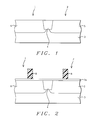
- Semiconductor substrate 3 comprised of single crystalline P type silicon, featuring a ⁇ 100> crystallographic orientation, is used and schematically shown in FIG. 1 .
- Region 1 of semiconductor substrate 3 , will be used for accommodation of P channel metal oxide semiconductor (PMOS), devices, while region 2 , will be used for accommodation of N channel metal oxide semiconductor (NMOS), devices.
- PMOS P channel metal oxide semiconductor
- NMOS N channel metal oxide semiconductor
- Insulator filled, shallow trench isolation (STI), region 4 is formed in a top portion of semiconductor substrate 3 , featuring formation of a shallow trench shape in semiconductor substrate 3 , accomplished via photolithographic and dry etching procedures, followed by filling of the shallow trench shape with a silicon oxide layer, in turn obtained via low pressure chemical vapor deposition (LPCVD), or plasma enhanced chemical vapor deposition (PECVD), procedures, using tetraethylorthosilicate (TEOS), as a source. Removal of portions of the silicon oxide layer from the top surface of semiconductor substrate 3 , is selectively accomplished via chemical mechanical polishing (CMP) procedures.
- CMP chemical mechanical polishing
- a photoresist shape (not shown in the drawings), is used to block out PMOS region 1 , from a procedure used to form P well region 5 , in NMOS region 2 . This is accomplished via implantation of boron, or BF 2 ions, at an energy between about 150 to 250 KeV, at dose between about 1E13 to 1E14 atoms/cm 2 .
- photoresist shape used to protect PMOS region 1 , from P well implantation procedures
- another photoresist shape is used to protect NMOS region 2 , from implantation of arsenic or phosphorous ions, implanted at an energy between about 300 to 600 KeV, and at a dose between about 1E13 to 1E14 atoms/cm 2 , allowing formation of N well region 6 , to be formed in PMOS region 1 .
- an anneal procedure is performed at a temperature between about 700 to 1000° C., employed to activate the implanted ions in both well regions. The result of these procedures is schematically shown in FIG. 1 .
- Silicon nitride layer 7 a is next deposited via LPCVD or PECVD procedures, at a thickness between about 10 to 500 Angstroms. If desired a composite layer, comprised of the silicon nitride layer on an underlying silicon oxide layer, can be use in place of silicon nitride layer 7 a .
- Photoresist shapes 8 are next formed on silicon nitride layer 7 a . This is schematically shown in FIG. 2 .
- An anisotropic RIE procedure using CF 4 or Cl 2 as an etchant, is first used to define silicon nitride shapes 7 b , using photoresist shapes 8 , as a mask.
- the anisotropic RIE procedure is then continued, using Cl 2 or SF 6 as an etchant for silicon, to selectively remove portions of semiconductor substrate 3 , not protected by photoresist shapes 8 , or occupied by STI region 4 , creating recessed regions 9 , in both PMOS region 1 , and in NMOS region 2 .
- the depth of recessed regions 9 , in semiconductor substrate 3 is between about 100 to 100,000 Angstroms. This is schematically shown in FIG. 3 .
- Photoresist shapes 8 are then removed via plasma oxygen ashing and careful wet cleans.
- Photoresist shape 10 is used as to protect NMOS region 2 , from implantation of boron or BF 2 ions, used to form heavily doped P type source/drain region 11 , in a top portion of recessed regions 9 , or N well region 6 , located in PMOS region 1 .
- the implantation procedure is performed at an energy between about 1 to 50 KeV, at a dose between about 1E12 to 5E12 atoms/cm 2 .
- photoresist block out shape 12 is defined, protecting PMOS region 1 , from implantation of N type ions, used to from heavily doped source/drain region 13 , in a top portion of recessed region 9 , or in P well region 5 , located in NMOS region 2 .
- Formation of heavily doped N type source/drain region 13 is accomplished via implantation of arsenic or phosphorous ions, at an energy between about 10 to 150 KeV, at a dose between about 1E12 to 1E16 atoms/cm 2 .
- an anneal procedure is performed at a temperature between about 500 to 1100° C., for a time between about 0 to 240 min, for purposes of activated the implanted ions in both heavily doped source/drain regions.
- the anneal procedure can be performed using either conventional furnace, or rapid thermal anneal procedures.
- the ion activating anneal procedure can be performed after deposition of a subsequent silicon oxide layer, or the activation of the implanted ions can occur during the deposition of the subsequent silicon oxide layer.
- Silicon oxide layer 14 shown schematically in FIG. 6, is next deposited via LPCVD or PECVD procedures, at a thickness between about 50 to 10,000 Angstroms, using a deposition temperature between about 300 to 700° C.
- Photoresist shape 45 is then employed as a masking shape, allowing the portions of silicon oxide layer 14 , to be entirely removed in PMOS region 1 . This is schematically shown in FIG. 7 . Removal of exposed portions of silicon oxide layer 14 , is accomplished either via wet etch procedures using a buffered hydrofluoric (BHF), or a dilute hydrofluoric (DHF), acid as etchant, or via an isotropic dry etch procedure, using CHF 3 as an etchant. Photoresist shape 45 , is then removed again via use of plasma oxygen ashing procedures.
- BHF buffered hydrofluoric
- DHF dilute hydrofluoric
- Polysilicon, or silicon layer 15 is next deposited via LPCVD procedures at a thickness between about 100 to 5000 Angstroms.
- Polysilicon layer 15 is in situ doped during deposition via the addition of diborane to a silane ambient.
- Polysilicon layer 15 directly interfaces the sides of the silicon nitride shape 7 b , as well as the sides of the non-recessed portion of semiconductor substrate 3 , in PMOS region 1 , while silicon oxide layer 14 , prevents direct overlay of polysilicon layer 15 , to silicon nitride shape 7 b , and to the non-recessed portion of semiconductor substrate 3 , located in NMOS region 2 .
- Photoresist shape 17 is next defined and used as an etch mask to protect PMOS region 1 , from etching procedures used to remove-exposed portions of silicon oxide layer 16 , polysilicon layer 15 , and silicon oxide layer 14 , located in NMOS region 2 . This is accomplished via isotropic RIE procedures using CHF 3 as an etchant for silicon oxide layer 16 , and silicon oxide layer 14 , while Cl 2 or SF 6 is used as an etchant for polysilicon layer 15 . This is schematically shown in FIG. 9 . Removal of photoresist shape 17 , is accomplished via plasma oxygen ashing procedures.
- polysilicon layer 18 is obtained via LPCVD procedures at a thickness between about 50 to 10,000 Angstroms, and is in situ doped via the addition of arsine, or phosphine, to a silane ambient.
- N type in situ doped polysilicon layer 18 is separated from underlying elements in PMOS region 1 , via silicon oxide layer 16 .
- Photoresist shape 19 is then used as a etch mask to allow portions of P type, in situ doped polysilicon layer 18 , as well as the remaining portion of silicon oxide layer 16 , to be removed in PMOS region 1 . This is accomplished via selective, isotropic dry etch procedures, using Cl 2 or SF 6 as an etchant for exposed regions of N type, in situ doped polysilicon layer 18 , while CHF 3 is used as an etchant for the remaining portion of silicon oxide layer 16 . The silicon oxide dry etching phase selectively terminates at the appearance of P type, in situ doped polysilicon layer 15 . The result of these selective dry etch procedures is schematically shown in FIG. 11 . Photoresist shape 19 , is removed via plasma oxygen ashing procedures.
- a critical, anisotropic RIE procedure is next performed, selectively removing portions of P type, in situ doped polysilicon layer 15 , located in PMOS region 1 , and portions of N type, in situ doped polysilicon layer 18 , located in NMOS region 2 .
- P type polysilicon spacers 55 will function as vertical, P type polysilicon, lightly doped source/drain (LDD), elements for the PMOS devices, while N type polysilicon spacers 58 , will function as vertical, N type polysilicon, LDD elements for the subsequent NMOS devices.
- the over-etch cycle used at the conclusion of the anisotropic RIE procedure used to define the spacers, results in recessing of the spacer structures, now positioned interfacing the center of the sides of silicon nitride shapes. The result of this procedure is schematically shown in FIG. 12 .
- a metal layer comprised of either titanium, tungsten, tantalum, nickel, or cobalt, is deposited via plasma vapor deposition procedures at a thickness between about 50 to 2000 Angstroms.
- Photoresist shapes 20 are next formed on the blanket metal layer and used as an etch mask to allow an anisotropic RIE procedure, using Cl 2 as an etchant, to define metal shapes 19 , overlying specific portions of the underlying, heavily doped source/drain regions.
- an anneal procedure is used to form metal silicide regions 21 , via consumption of portions of the heavily doped source/drain regions.
- the anneal procedure can be performed using a rapid thermal anneal (RTA) procedure, at a temperature between about 200 to 800° C., for a time between about 0 to 30 min, in an inert ambient, or performed via conventional furnace procedures at a temperature between about 200 to 800° C., for a time between about 0 to 240 min, again performed in an inert ambient.
- RTA rapid thermal anneal
- Metal silicide regions 21 are then comprised of titanium silicide, tungsten silicide, tantalum silicide, nickel silicide, or cobalt silicide.
- Insulator layer 22 comprised of a low k layer such as silicon oxide, boro-phosphosilicate glass (BPSG), or phosphosilicate glass (PSG), is next deposited via LPCVD or PECVD procedures, to a thickness between about 1000 to 100,000 Angstroms.
- a chemical mechanical polishing (CMP), procedure is then used to planarize insulator layer 22 , selectively terminating at the appearance of the top surface of silicon nitride shapes 7 b . This is schematically shown in FIG. 15 .
- Silicon nitride shapes 7 b are now selectively removed via a wet etch procedure, using a hot phosphoric acid solution.
- silicon nitride shapes 7 b can be selectively removed via a dry etch procedure, using Cl 2 as a selective etchant for silicon nitride.
- the removal of silicon nitride shapes 7 b creates opening 23 , exposing the underlying non-recessed portion of semiconductor substrate 3 , and located surrounded by the top portions of LDD spacer elements, specifically P type polysilicon spacer 55 , in PMOS region 1 , and N type polysilicon spacer 58 , located in NMOS region 2 . This is schematically illustrated in FIG. 16 .
- a critical deposition of high k metal oxide layer 24 is next accomplished via metal organic chemical vapor deposition (MOCVD), or via atomic layer chemical vapor deposition (ALCVD) procedures to a thickness between about 10 to 1000 Angstroms, at a temperature between about 100 to 1000° C., using HfCl 4 , ZrCl 4 , AlCl 3 , as reactants for the ALCVD procedure, while using tetrakis dimethyl amino hafnium (TDMAH), or TDMAZ as reactants for the MOCVD procedure.
- High k metal oxide layer 24 featuring a dielectric constant between about 7 to 500, allows the use of a thicker layer.
- the higher dielectric constant layer allows an equivalent oxide thickness (EOT), equal to the thinner, lower k dielectric counterparts, to be realized.
- EOT equivalent oxide thickness
- High k metal oxide layer 24 comprised of aluminum oxide (Al 2 O 3 ), zirconium oxide (ZrO 2 ), or halfnium oxide (HfO 2 ), completely fills openings 23 , with a portion of the high k dielectric layer residing on the top surface of insulator layer 22 .
- Conductive layer 25 comprised of a metal, or metal silicide layer such as aluminum, aluminum-copper, copper, tungsten, or tungsten silicide, is next deposited on high k dielectric layer 24 , via plasma vapor deposition procedures, at a thickness between about 100 to 10,000 Angstroms. If desired conductive layer 25 , can be comprised of an in situ doped polysilicon layer. Photoresist shapes 26 , are then formed and used as an etch mask to allow an anisotropic RIE procedure, to define the gate, or metal structure 25 , as well as removing unprotected portions of high k dielectric layer 24 .
- a metal, or metal silicide layer such as aluminum, aluminum-copper, copper, tungsten, or tungsten silicide
- Each metal oxide semiconductor field effect transistor (MOSFET), device is now comprised of: lateral, heavily doped source/drain regions; lateral channel regions located in the non-recessed portion of semiconductor substrate 3 , underlying a gate dielectric layer comprised of a high k dielectric layer; vertical LDD polysilicon spacers; and a conductive gate structure, self-aligned to the underlying high k dielectric layer.
- MOSFET metal oxide semiconductor field effect transistor
- interlevel dielectric (ILD) layer 27 comprised of either BPSG, PSG, or silicon oxide, is deposited via LPCVD or PECVD procedures, at a thickness between about 100 to 10,000 Angstroms. This is schematically shown in FIG. 18 . If desired ILD layer 27 , can be subjected to a CMP procedure for planarization purposes.
- a photoresist shape (not shown in the drawings), is then used as a mask to allow an anisotropic RIE procedure to define contact hole openings 28 , exposing portions of top surfaces of metal gate structures 25 , as well as metal silicide regions 21 , located in PMOS region 1 , as well as in NMOS region 2 .
- the anisotropic RIE procedure is performed using CHF 3 as a selective etchant for ILD layer 27 , and for insulator layer 22 .
- a metal layer such as aluminum, aluminum-copper, copper, or tungsten, is deposited via plasma vapor deposition procedures, completely filling all contact hole openings, as well as overlying the top surface of ILD layer 27 .
- Another photoresist shape (not shown in the drawings), is formed and used as a mask to allow an anisotropic RIE procedure, using Cl 2 as an etchant, to define metal structures in contact hole openings 28 .
- Metal structures 29 a , 29 b , and 29 c now communicate with a heavily doped source region, a metal gate structure, and a heavily doped drain region, respectfully, in PMOS region 1 , while metal structures 29 d , 29 e , and 29 f , are used for contact to a heavily doped source region, a metal gate structure, and a heavily doped drain region, respectfully, in NMOS region 2 .
- the result of these procedures is schematically shown in FIG. 19 .
- the photoresist shape used to define the metal structures is now removed via plasma oxygen ashing procedures.
Abstract
A CMOS device structure, and a method of fabricating the CMOS device, featuring a gate insulator layer comprised of a high k metal oxide layer, has been developed. The process features formation of recessed, heavily doped source/drain regions, and of vertical, polysilicon LDD spacers, prior to deposition of the high k metal oxide layer. Removal of a silicon nitride shape, previously used as a mask for definition of the recessed regions, which in turn are used for accommodation of the heavily doped source/drain regions, provides the space to be occupied by the high k metal oxide layer. The integrity of the high k, gate insulator layer, butted by the vertical polysilicon spacers, and overlying a channel region provided by the non-recessed portion of the semiconductor substrate, is preserved via delayed deposition of the metal oxide layer, performed after high temperature anneals such as the activation anneal for heavily doped source/drain regions, as well as the anneal used for metal silicide formation.
Description
(1) Field of the Invention
The present invention relates to methods used to fabricate semiconductor devices, and more specifically to a method used to integrate a gate insulator layer, comprised of a high dielectric constant (high k), material, into a CMOS device process sequence.
(2) Description of Prior Art
The advent of micro-miniaturization, or the ability to fabricate semiconductor devices with sub-micron features, has allowed device performance, as well as processing costs, to be reduced. The use of sub-micron features has resulted in reductions in performance degrading parasitic capacitances, while a greater amount of smaller semiconductor chips, comprised with sub-micron features, can now be obtained from a specific size substrate, thus reducing the processing cost for a specific semiconductor chip. The continuous scaling down of device dimensions necessitates the use of thinner gate insulator layers, and as the thickness of silicon dioxide layers used as a gate insulator layer decreases, integrity and leakage concerns, not present for gate insulator layers comprised of thicker silicon dioxide layers, become evident. The use of high k dielectric layers as gate insulator layers allow thicker layers to be used, with the thicker, high k dielectric layer supplying capacitances equal to thinner silicon oxide layers, or with the high k dielectric layer having an equivalent oxide thickness (EOT), equal to the thinner silicon dioxide counterpart layer. Therefore the use of high k dielectric layers, for gate insulator layer, will offer reduced leakage when compared to the thicker silicon dioxide gate insulator counterparts.
Metal oxide layers, such as aluminum oxide (Al2O3), zirconium oxide (ZrO2), and hafnium oxide (HfO2), are examples of high k dielectric layers, attractive as gate insulator layers for sub-micron devices, however the thermal stability of the metal oxide layers can be a problem when a gate metal insulator is formed prior to subsequent processing steps such as source/drain activation anneals, and metal silicide formation. The temperatures reached during these procedures can result in crystallization of the high k, metal oxide layer, resulting in undesirable gate leakage or shorts. This invention will describe a novel process procedure, and device structure, in which a high k, metal oxide layer is used as the device gate insulator layer, however formed and defined after high temperature anneals, and silicide formation procedures. Prior art, such as Wu, in U.S. Pat. No. 5,972,762, as well as Cha, in U.S. Pat. No. 5,970,329, describe methods of forming recessed elements in metal oxide semiconductor field effect (MOSFET), devices, however these prior arts do not describe the novel device process sequence, and novel process structure, illustrated in this present invention in which a device gate insulator layer, comprised of a high k, metal oxide layer, is integrated into a CMOS device process sequence after high temperature processes have been completed.
It is an object of this invention to fabricate a complimentary metal oxide semiconductor (CMOS) device featuring a high k dielectric layer for use as a gate insulator layer.
It is another object of this invention to integrate a high k, metal oxide, gate layer, into a CMOS fabrication sequence, after high temperature source/drain anneals, and high temperature metal silicide layer formation procedures, have been performed.
It is still another object of this invention to form the high k, metal oxide gate layer in a space surrounded by lightly doped source/drain (LDD), silicon spacers, wherein the space was created by removal of a silicon nitride masking shape, which in turn is used to define recessed source/drain regions as well as to define word lines.
In accordance with the present invention a method of integrating the formation of a high k, gate insulator layer into a CMOS fabrication procedure, at a stage of the CMOS fabrication procedure after which high temperature procedures have already been performed, is described. After formation of an N well, and of a P well region, for accommodation of P channel (PMOS), and N channel (NMOS), devices, a silicon nitride shape is formed on the surface of the well regions and used as a mask to selectively remove, and recess, unprotected silicon regions. Heavily doped P type, and N type, source/drain regions are then formed in the recessed portions in the P and N well regions, via ion implantation and annealing procedures, used to activate the implanted ions. Deposition of in situ doped polysilicon layers, and dry etching procedures, result in the formation of P type, and N type, lightly doped source/drain (LDD), spacers, on the sides of the silicon nitride shapes, as well as on the sides of the non-recessed silicon shapes, underlying the silicon nitride masking shapes. Metal silicide regions are next formed in portions of both the P type, and N type heavily doped source/drain region, via formation of a metal shape followed by anneal procedure. After formation of a planarizing insulator layer, the silicon nitride shapes are removed, exposing the surrounding LDD spacers, and exposing underlying non-recessed silicon, located between he heavily doped source/drain regions. A high k, metal oxide layer is deposited, filling the space vacated by the silicon nitride shape, followed by deposition of a conductive layer. Patterning procedures are used to define a conductive gate structure, overlying the high k, metal oxide gate insulator layer. Deposition of, and planarization of, an overlying insulator layer, is followed by definition of contact openings in the insulator layer, exposing portions of top surfaces of the recessed, highly doped source/drain regions, as well as portions of the top surface of the conductive gate structures. Deposition of, and patterning of, a metal layer, results in creation of metal contact and interconnect structures located in the contact openings.
The object and other advantages of this invention are best described in the preferred embodiments with reference to the attached drawings that include:
FIGS. 1-19, which schematically, in cross-sectional style, describe key stages of fabrication used to integrate the formation of a high k, gate layer into a CMOS fabrication procedure, at a stage of the CMOS fabrication procedure at which high temperature procedures, such as source/drain anneal, and metal silicide formation, have previously been performed.
The method of forming a complimentary metal oxide semiconductor (CMOS) device featuring a high k, gate insulator layer, integrating into the CMOS fabrication procedure after high temperature procedures, such as source/drain anneal, and metal silicide formation, have previously been performed, will now be described in detail. Semiconductor substrate 3, comprised of single crystalline P type silicon, featuring a <100> crystallographic orientation, is used and schematically shown in FIG. 1. Region 1, of semiconductor substrate 3, will be used for accommodation of P channel metal oxide semiconductor (PMOS), devices, while region 2, will be used for accommodation of N channel metal oxide semiconductor (NMOS), devices. Insulator filled, shallow trench isolation (STI), region 4, is formed in a top portion of semiconductor substrate 3, featuring formation of a shallow trench shape in semiconductor substrate 3, accomplished via photolithographic and dry etching procedures, followed by filling of the shallow trench shape with a silicon oxide layer, in turn obtained via low pressure chemical vapor deposition (LPCVD), or plasma enhanced chemical vapor deposition (PECVD), procedures, using tetraethylorthosilicate (TEOS), as a source. Removal of portions of the silicon oxide layer from the top surface of semiconductor substrate 3, is selectively accomplished via chemical mechanical polishing (CMP) procedures. A photoresist shape, (not shown in the drawings), is used to block out PMOS region 1, from a procedure used to form P well region 5, in NMOS region 2. This is accomplished via implantation of boron, or BF2 ions, at an energy between about 150 to 250 KeV, at dose between about 1E13 to 1E14 atoms/cm2. After removal of the photoresist shape used to protect PMOS region 1, from P well implantation procedures, another photoresist shape, (not shown in the drawings), is used to protect NMOS region 2, from implantation of arsenic or phosphorous ions, implanted at an energy between about 300 to 600 KeV, and at a dose between about 1E13 to 1E14 atoms/cm2, allowing formation of N well region 6, to be formed in PMOS region 1. After removal of the NMOS region 2, photoresist block out shape, an anneal procedure is performed at a temperature between about 700 to 1000° C., employed to activate the implanted ions in both well regions. The result of these procedures is schematically shown in FIG. 1.
The formation of heavily doped P type, and N type source/drain regions, in the recessed regions of semiconductor substrate 3, is next addressed, and schematically described using FIGS. 4-5. Photoresist shape 10, is used as to protect NMOS region 2, from implantation of boron or BF2 ions, used to form heavily doped P type source/drain region 11, in a top portion of recessed regions 9, or N well region 6, located in PMOS region 1. The implantation procedure is performed at an energy between about 1 to 50 KeV, at a dose between about 1E12 to 5E12 atoms/cm2. After removal of photoresist shape 10, via plasma oxygen ashing, photoresist block out shape 12, is defined, protecting PMOS region 1, from implantation of N type ions, used to from heavily doped source/drain region 13, in a top portion of recessed region 9, or in P well region 5, located in NMOS region 2. Formation of heavily doped N type source/drain region 13, is accomplished via implantation of arsenic or phosphorous ions, at an energy between about 10 to 150 KeV, at a dose between about 1E12 to 1E16 atoms/cm2. After removal of photoresist shape 12, via plasma oxygen ashing procedures, an anneal procedure is performed at a temperature between about 500 to 1100° C., for a time between about 0 to 240 min, for purposes of activated the implanted ions in both heavily doped source/drain regions. The anneal procedure can be performed using either conventional furnace, or rapid thermal anneal procedures. In addition the ion activating anneal procedure can be performed after deposition of a subsequent silicon oxide layer, or the activation of the implanted ions can occur during the deposition of the subsequent silicon oxide layer.
Polysilicon, or silicon layer 15, is next deposited via LPCVD procedures at a thickness between about 100 to 5000 Angstroms. Polysilicon layer 15, is in situ doped during deposition via the addition of diborane to a silane ambient. Polysilicon layer 15, directly interfaces the sides of the silicon nitride shape 7 b, as well as the sides of the non-recessed portion of semiconductor substrate 3, in PMOS region 1, while silicon oxide layer 14, prevents direct overlay of polysilicon layer 15, to silicon nitride shape 7 b, and to the non-recessed portion of semiconductor substrate 3, located in NMOS region 2. After deposition of polysilicon layer 15, silicon oxide layer 16, is deposited via LPCVD or PECVD procedures, at a thickness between about 50 to 10,000 Angstroms. The result of these depositions is schematically shown in FIG. 8. Photoresist shape 17, is next defined and used as an etch mask to protect PMOS region 1, from etching procedures used to remove-exposed portions of silicon oxide layer 16, polysilicon layer 15, and silicon oxide layer 14, located in NMOS region 2. This is accomplished via isotropic RIE procedures using CHF3 as an etchant for silicon oxide layer 16, and silicon oxide layer 14, while Cl2 or SF6 is used as an etchant for polysilicon layer 15. This is schematically shown in FIG. 9. Removal of photoresist shape 17, is accomplished via plasma oxygen ashing procedures.
The removal of the silicon oxide and P type, in situ doped polysilicon from NMOS region 2, allows polysilicon layer 18, to now be deposited and to directly interface the sides of silicon nitride shape 7 b, as well as the sides of the non-recessed portion of semiconductor substrate 3, located in NMOS region 2. Polysilicon layer 18, schematically shown in FIG. 10, is obtained via LPCVD procedures at a thickness between about 50 to 10,000 Angstroms, and is in situ doped via the addition of arsine, or phosphine, to a silane ambient. N type in situ doped polysilicon layer 18, is separated from underlying elements in PMOS region 1, via silicon oxide layer 16. Photoresist shape 19, is then used as a etch mask to allow portions of P type, in situ doped polysilicon layer 18, as well as the remaining portion of silicon oxide layer 16, to be removed in PMOS region 1. This is accomplished via selective, isotropic dry etch procedures, using Cl2 or SF6 as an etchant for exposed regions of N type, in situ doped polysilicon layer 18, while CHF3 is used as an etchant for the remaining portion of silicon oxide layer 16. The silicon oxide dry etching phase selectively terminates at the appearance of P type, in situ doped polysilicon layer 15. The result of these selective dry etch procedures is schematically shown in FIG. 11. Photoresist shape 19, is removed via plasma oxygen ashing procedures.
A critical, anisotropic RIE procedure is next performed, selectively removing portions of P type, in situ doped polysilicon layer 15, located in PMOS region 1, and portions of N type, in situ doped polysilicon layer 18, located in NMOS region 2. This is accomplished using Cl2 or SF6 as an etchant, resulting in the formation of P type polysilicon spacers 55, located on the sides of silicon nitride shape 7 b, and on the sides of the non-recessed portion of semiconductor substrate 3, located in PMOS region 1, and resulting in the formation of N type polysilicon spacers 58, located on the sides of silicon nitride shape 7 b, and on the sides of the nonrecessed portion of semiconductor substrate 3, located in NMOS region 1. P type polysilicon spacers 55, will function as vertical, P type polysilicon, lightly doped source/drain (LDD), elements for the PMOS devices, while N type polysilicon spacers 58, will function as vertical, N type polysilicon, LDD elements for the subsequent NMOS devices. The over-etch cycle, used at the conclusion of the anisotropic RIE procedure used to define the spacers, results in recessing of the spacer structures, now positioned interfacing the center of the sides of silicon nitride shapes. The result of this procedure is schematically shown in FIG. 12.
Formation of metal silicide layers on portions of both type heavily doped source/drain regions is next addressed and schematically described using FIGS. 13-14. A metal layer, comprised of either titanium, tungsten, tantalum, nickel, or cobalt, is deposited via plasma vapor deposition procedures at a thickness between about 50 to 2000 Angstroms. Photoresist shapes 20, are next formed on the blanket metal layer and used as an etch mask to allow an anisotropic RIE procedure, using Cl2 as an etchant, to define metal shapes 19, overlying specific portions of the underlying, heavily doped source/drain regions. After removal of photoresist shapes 20, via plasma oxygen ashing, an anneal procedure is used to form metal silicide regions 21, via consumption of portions of the heavily doped source/drain regions. The anneal procedure can be performed using a rapid thermal anneal (RTA) procedure, at a temperature between about 200 to 800° C., for a time between about 0 to 30 min, in an inert ambient, or performed via conventional furnace procedures at a temperature between about 200 to 800° C., for a time between about 0 to 240 min, again performed in an inert ambient. Metal silicide regions 21, are then comprised of titanium silicide, tungsten silicide, tantalum silicide, nickel silicide, or cobalt silicide.
A critical deposition of high k metal oxide layer 24, is next accomplished via metal organic chemical vapor deposition (MOCVD), or via atomic layer chemical vapor deposition (ALCVD) procedures to a thickness between about 10 to 1000 Angstroms, at a temperature between about 100 to 1000° C., using HfCl4, ZrCl4, AlCl3, as reactants for the ALCVD procedure, while using tetrakis dimethyl amino hafnium (TDMAH), or TDMAZ as reactants for the MOCVD procedure. High k metal oxide layer 24, featuring a dielectric constant between about 7 to 500, allows the use of a thicker layer. The higher dielectric constant layer allows an equivalent oxide thickness (EOT), equal to the thinner, lower k dielectric counterparts, to be realized. In addition the increased thickness, acceptable via use of the higher k dielectric layer, reduces the risk of gate insulator leakage or shorts, again when compared to thinner, low k dielectric layers. High k metal oxide layer 24, comprised of aluminum oxide (Al2O3), zirconium oxide (ZrO2), or halfnium oxide (HfO2), completely fills openings 23, with a portion of the high k dielectric layer residing on the top surface of insulator layer 22. Conductive layer 25, comprised of a metal, or metal silicide layer such as aluminum, aluminum-copper, copper, tungsten, or tungsten silicide, is next deposited on high k dielectric layer 24, via plasma vapor deposition procedures, at a thickness between about 100 to 10,000 Angstroms. If desired conductive layer 25, can be comprised of an in situ doped polysilicon layer. Photoresist shapes 26, are then formed and used as an etch mask to allow an anisotropic RIE procedure, to define the gate, or metal structure 25, as well as removing unprotected portions of high k dielectric layer 24. The anisotropic RIE procedure is performed using Cl2 as a selective etchant for metal or metal silicide, while HF is used as an etchant for high k dielectric layer 24. The result of this procedure is schematically shown in FIG. 17. Each metal oxide semiconductor field effect transistor (MOSFET), device is now comprised of: lateral, heavily doped source/drain regions; lateral channel regions located in the non-recessed portion of semiconductor substrate 3, underlying a gate dielectric layer comprised of a high k dielectric layer; vertical LDD polysilicon spacers; and a conductive gate structure, self-aligned to the underlying high k dielectric layer.
After removal of photoresist shapes 26, via plasma oxygen ashing, interlevel dielectric (ILD), layer 27, comprised of either BPSG, PSG, or silicon oxide, is deposited via LPCVD or PECVD procedures, at a thickness between about 100 to 10,000 Angstroms. This is schematically shown in FIG. 18. If desired ILD layer 27, can be subjected to a CMP procedure for planarization purposes. A photoresist shape (not shown in the drawings), is then used as a mask to allow an anisotropic RIE procedure to define contact hole openings 28, exposing portions of top surfaces of metal gate structures 25, as well as metal silicide regions 21, located in PMOS region 1, as well as in NMOS region 2. The anisotropic RIE procedure is performed using CHF3 as a selective etchant for ILD layer 27, and for insulator layer 22. After removal of the photoresist shape used to define the contact hole openings, a metal layer such as aluminum, aluminum-copper, copper, or tungsten, is deposited via plasma vapor deposition procedures, completely filling all contact hole openings, as well as overlying the top surface of ILD layer 27. Another photoresist shape (not shown in the drawings), is formed and used as a mask to allow an anisotropic RIE procedure, using Cl2 as an etchant, to define metal structures in contact hole openings 28. Metal structures 29 a, 29 b, and 29 c, now communicate with a heavily doped source region, a metal gate structure, and a heavily doped drain region, respectfully, in PMOS region 1, while metal structures 29 d, 29 e, and 29 f, are used for contact to a heavily doped source region, a metal gate structure, and a heavily doped drain region, respectfully, in NMOS region 2. The result of these procedures is schematically shown in FIG. 19. The photoresist shape used to define the metal structures is now removed via plasma oxygen ashing procedures.
While this invention has been particularly shown and described with reference to the preferred embodiments thereof, it will be understood by those skilled in the art that various changes in form and details may be made without departing from the spirit or scope of the invention.
Claims (29)
1. A method of forming a metal oxide semiconductor field effect transistor (MOSFET) device, with a gate insulator layer comprised of a high dielectric constant (high k), dielectric layer, on a semiconductor substrate, comprising the steps of:
forming a well region in a top portion of said semiconductor substrate,
forming a hard mask on a portion of top surface of said semiconductor substrate;
performing a first dry etch procedure to remove a top portion of said semiconductor substrate not covered by said hard mask, resulting in recessed regions in said semiconductor substrate, and a non-recessed portion of said semiconductor substrate covered by said hard mask;
forming a heavily doped source/drain region in a top portion of said recessed regions;
depositing a polysilicon layer;
performing a second dry etch procedure to form lightly doped source/drain (LDD), polysilicon spacers on the sides of said non-recessed portion of said semiconductor substrate;
forming a metal silicide region in a top portion of said heavily doped source/drain region;
forming a planarized first insulator layer, exposing top surface of said hard mask;
removing said hard mask resulting in space located between LDD polysilicon spacers, exposing top surface of underlying said non-recessed portion of said semiconductor substrate;
forming said gate insulator layer, comprised of said high k dielectric layer, in said space; and
forming a conductive metal structure on said gate insulator layer.
2. The method of claim 1 , wherein said well region is a P well region, obtained via implantation of boron or BF2 ions, at an energy between about 150 to 250 KeV, at a dose between about 1E13 to 1E14 atoms/cm2.
3. The method of claim 1 , wherein said well region is an N well region, obtained via implantation of arsenic or phosphorous ions, at an energy between about 300 to 600 KeV, at a dose between about 1E13 to 1E14 atoms/cm2.
4. The method of claim 1 , wherein said hard mask is a silicon nitride shape, formed from a silicon nitride layer, in turn obtained via LPCVD or PECVD procedures, at a thickness between about 10 to 500 Angstroms.
5. The method of claim 1 , wherein the depth of said recessed regions in said semiconductor substrate is between about 100 to 100,000 Angstroms.
6. The method of claim 1 , wherein said heavily doped source/drain region is a P type, heavily doped source/drain region, obtained via implantation of boron or BF2 ions, at an energy between about 1 to 50 KeV, and at a dose between about 1E12 to 5E15 atoms/cm2 .
7. The method of claim 1 , wherein said heavily doped source/drain region is an N type, heavily doped source/drain region, obtained via implantation of arsenic or phosphorous ions, at an energy between about 10 to 150 KeV, and at a dose between about 1E12 to 1E16 atoms/cm2 .
8. The method of claim 1 , wherein said polysilicon layer is a P type in situ doped polysilicon layer, obtained via LPCVD procedures at a thickness between about 100 to 5000 Angstroms, and doped via the addition of diborane to a silane ambient.
9. The method of claim 1 , wherein said polysilicon layer is an N type in situ doped polysilicon layer, obtained via LPCVD procedures at a thickness between about 100 to 5000 Angstroms, and doped via the addition of arsine, or phosphine, to a silane ambient.
10. The method of claim 1 , wherein second dry etch procedure, used to form said LDD polysilicon spacers, is an anisotropic RIE procedure, using Cl2 or SF6 as an etchant for said in situ doped polysilicon layer.
11. The method of claim 1 , wherein said hard mask is selectively removed via wet etch procedures using a hot phosphoric acid solution.
12. The method of claim 1 , wherein said hard mask is selectively removed via a dry etch procedure using Cl2 as an etchant.
13. The method of claim 1 , wherein said high k dielectric layer, used for said gate insulator layer, is comprised of either aluminum oxide (Al2O3), zirconium oxide (ZrO2), or hafnium oxide (HfO2), obtained at a thickness between about 10 to 1000 Angstroms, via metal organic chemical vapor deposition (MOCVD), or via atomic layer chemical vapor deposition (ALCVD) procedures, performed at a temperature between about 100 to 1000° C., using HfCl4 or ZrCl4 as reactants for the ALCVD procedure, or using tetrakis dimethyl amino hafnium (TDMAH), or TDMAZ), as reactants for the MOCVD procedure.
14. The method of claim 1 , wherein said high k dielectric layer is comprised with a dielectric constant between about 7 to 100.
15. The method of claim 1 , wherein said conductive gate structure is comprised of either a metal layer such as tungsten, aluminum, aluminum-copper, or copper, a metal silicide layer such as tungsten silicide, or a doped polysilicon layer.
16. A method of fabricating a complementary metal oxide semiconductor (CMOS) device on a semiconductor substrate, comprised of a P channel metal oxide semiconductor (PMOS), device, and of an N channel metal oxide semiconductor (NMOS), device, and featuring a gate insulator layer comprised of a high k metal oxide layer formed after completion of high temperature process steps, comprising the steps of:
providing a PMOS region in a first area of said semiconductor substrate to be used for said PMOS device, and providing an NMOS region in a second area of said semiconductor substrate to be used for said NMOS device;
forming an N well region in a top portion of said PMOS region;
forming a P well region in a top portion of said N well region;
depositing a silicon nitride layer;
performing a first anisotropic RIE procedure to define a silicon nitride shape, and to recess a top portion of said semiconductor substrate, in said PMOS and in said NMOS regions, resulting in a non-recessed portion of said semiconductor substrate, overlaid by said silicon nitride shape, in said PMOS region and in said NMOS regions;
performing a first ion implantation procedure to form a P type heavily doped source/drain region in a first recessed region located in said PMOS region;
performing a second ion implantation procedure to form an N type heavily doped source/drain region in a second recessed region located in said NMOS region;
depositing a first silicon oxide layer;
removing portion of said first silicon oxide layer located in said PMOS region;
depositing a P type, in situ doped polysilicon layer;
depositing a second silicon oxide layer;
removing portion of said second silicon oxide layer, portion of said P type, in situ doped polysilicon layer, and portion of said first silicon oxide layer located in said NMOS region;
depositing an N type, in situ doped polysilicon layer;
removing portion of said N type, in situ doped polysilicon layer and portion of said second silicon oxide layer located in said PMOS region, resulting in a remaining portion of said P type, in situ doped polysilicon layer in said PMOS region, and resulting in a remaining portion of said N type, in situ doped polysilicon layer located in said NMOS region;
performing a second anisotropic RIE procedure to form P type polysilicon, lightly doped source/drain (LDD), spacers on the sides of non-recessed portion of said semiconductor substrate and on the sides of a bottom portion of said silicon nitride shape, in said PMOS region, and to form N type polysilicon, LDD spacers on the sides of non-recessed portion of said semiconductor substrate and on the sides of a bottom portion of said silicon nitride shape, in said NMOS region;
depositing a first metal layer;
performing a patterning procedure to define metal shapes on the top surface of said P type heavily doped source/drain region, and on the top surface of said N type heavily doped source/drain region;
performing an anneal procedure to form metal silicide regions in said P type heavily doped source/drain region, and in said N type heavily doped source/drain region;
depositing a first insulator layer;
performing a chemical mechanical polishing procedure planarizing top surface of said first insulator layer and exposing the top surface of the silicon nitride shapes;
removing said silicon nitride shapes resulting in spaces located between polysilicon LDD spacers, exposing the top surfaces of the recessed portions of said semiconductor substrate;
depositing said high k metal oxide layer, completely filling said spaces;
depositing a second metal layer;
performing a third anisotropic RIE procedure to define metal gate structures, and to define gate insulator shape, comprised of said high k metal oxide layer;
depositing a second insulator layer;
forming contact hole openings in a second insulator layer and in said first insulator layer, exposing portions of top surfaces of said P type heavily doped source/drain region, of said N type heavily doped source/drain region, and of said metal gate structures; and
forming metal contact structures in said contact hole openings.
17. The method of claim 16 , wherein said silicon nitride layer is obtained via LPCVD or PECVD procedures, at a thickness between about 10 to 500 Angstroms.
18. The method of claim 16 , wherein the depth of said recess, located in said top portion of said semiconductor substrate, is between about 100 to 100,000 Angstroms.
19. The method of claim 16 , wherein said first ion implantation procedure used to create said P type heavily doped source/drain region, is performed via implantation of boron or BF2 ions, at an energy between about 1 to 50 KeV, and at a dose between about 1E12 to 5E15 atoms/cm2.
20. The method of claim 16 , wherein said second ion implantation procedure used to create said N type heavily doped source/drain region, is performed via implantation of arsenic or phosphorous ions, at an energy between about 10 to 150 KeV, and at a dose between about 1E12 to 1E16 atoms/cm2.
21. The method of claim 16 , wherein said P type, in situ doped polysilicon layer is obtained via LPCVD procedures at a thickness between about 100 to 5000 Angstroms, and doped via the addition of diborane to a silane ambient.
22. The method of claim 16 , wherein said N type, in situ doped polysilicon layer is obtained via LPCVD procedures at a thickness between about 100 to 5000 Angstroms, and doped via the addition arsine, or phosphine, to a silane ambient.
23. The method of claim 16 , wherein second anisotropic RIE procedure, used to form said P type polysilicon, LDD spacers and said N type polysilicon, LDD spacers, is performed using Cl2 or SF6 as an etchant for polysilicon.
24. The method of claim 16 , wherein said silicon nitride shapes are selectively removed via wet etch procedures using a hot phosphoric acid solution.
25. The method of claim 16 , wherein said silicon nitride shapes are selectively removed via a dry etch procedure using Cl2 as an etchant.
26. The method of claim 16 , wherein said high k metal oxide layer used for said gate insulator layer is comprised of either aluminum oxide (Al2O3), zirconium oxide (ZrO2), or hafnium oxide (HfO2), obtained at a thickness between about 10 to 1000 Angstroms, via metal organic chemical vapor deposition (MOCVD), or via atomic layer chemical vapor deposition procedures, performed at a temperature between about 100 to 1000° C., using HfCl4 or ZrCl4 as reactants for the ALCVD procedure, or using tetrakis dimethyl amino hafnium (TDMAH), or TDMAZ), as reactants for the MOCVD procedure.
27. The method of claim 16 , wherein said high k metal oxide layer is comprised with a dielectric constant between about 7 to 100.
28. The method of claim 16 , wherein said second metal layer, used-for said metal gate structures, is either a tungsten, aluminum, aluminum-copper, or copper layer.
29. The method of claim 16 , wherein said metal gate structures are defined from a metal silicide layer such as tungsten silicide, or from a doped polysilicon layer.
Priority Applications (3)
| Application Number | Priority Date | Filing Date | Title |
|---|---|---|---|
| US10/146,287 US6656764B1 (en) | 2002-05-15 | 2002-05-15 | Process for integration of a high dielectric constant gate insulator layer in a CMOS device |
| US10/696,007 US6914313B2 (en) | 2002-05-15 | 2003-10-29 | Process for integration of a high dielectric constant gate insulator layer in a CMOS device |
| US11/119,951 US7393766B2 (en) | 2002-05-15 | 2005-05-02 | Process for integration of a high dielectric constant gate insulator layer in a CMOS device |
Applications Claiming Priority (1)
| Application Number | Priority Date | Filing Date | Title |
|---|---|---|---|
| US10/146,287 US6656764B1 (en) | 2002-05-15 | 2002-05-15 | Process for integration of a high dielectric constant gate insulator layer in a CMOS device |
Related Child Applications (1)
| Application Number | Title | Priority Date | Filing Date |
|---|---|---|---|
| US10/696,007 Division US6914313B2 (en) | 2002-05-15 | 2003-10-29 | Process for integration of a high dielectric constant gate insulator layer in a CMOS device |
Publications (1)
| Publication Number | Publication Date |
|---|---|
| US6656764B1 true US6656764B1 (en) | 2003-12-02 |
Family
ID=29548284
Family Applications (3)
| Application Number | Title | Priority Date | Filing Date |
|---|---|---|---|
| US10/146,287 Expired - Lifetime US6656764B1 (en) | 2002-05-15 | 2002-05-15 | Process for integration of a high dielectric constant gate insulator layer in a CMOS device |
| US10/696,007 Expired - Fee Related US6914313B2 (en) | 2002-05-15 | 2003-10-29 | Process for integration of a high dielectric constant gate insulator layer in a CMOS device |
| US11/119,951 Expired - Lifetime US7393766B2 (en) | 2002-05-15 | 2005-05-02 | Process for integration of a high dielectric constant gate insulator layer in a CMOS device |
Family Applications After (2)
| Application Number | Title | Priority Date | Filing Date |
|---|---|---|---|
| US10/696,007 Expired - Fee Related US6914313B2 (en) | 2002-05-15 | 2003-10-29 | Process for integration of a high dielectric constant gate insulator layer in a CMOS device |
| US11/119,951 Expired - Lifetime US7393766B2 (en) | 2002-05-15 | 2005-05-02 | Process for integration of a high dielectric constant gate insulator layer in a CMOS device |
Country Status (1)
| Country | Link |
|---|---|
| US (3) | US6656764B1 (en) |
Cited By (42)
| Publication number | Priority date | Publication date | Assignee | Title |
|---|---|---|---|---|
| US20040087075A1 (en) * | 2002-05-15 | 2004-05-06 | Taiwan Semiconductor Manufacturing Company | Process for integration of a high dielectric constant gate insulator layer in a CMOS device |
| US20050040490A1 (en) * | 2003-08-19 | 2005-02-24 | Park Nam Kyu | Transistor in semiconductor device and method of manufacturing the same |
| US20050151166A1 (en) * | 2004-01-09 | 2005-07-14 | Chun-Chieh Lin | Metal contact structure and method of manufacture |
| US20050167779A1 (en) * | 2004-02-02 | 2005-08-04 | Atmel Germany Gmbh | Process for manufacturing vertically insulated structural components on SOI material of various thickness |
| US20050186747A1 (en) * | 2004-02-25 | 2005-08-25 | International Business Machines Corporation | CMOS silicide metal gate integration |
| US20050205896A1 (en) * | 2004-03-18 | 2005-09-22 | Hong-Jyh Li | Transistor with dopant-bearing metal in source and drain |
| US20050282329A1 (en) * | 2004-06-17 | 2005-12-22 | Hong-Jyh Li | CMOS transistors with dual high-k gate dielectric and methods of manufacture thereof |
| US20060011905A1 (en) * | 2003-06-26 | 2006-01-19 | Rj Mears, Llc | Semiconductor device comprising a superlattice dielectric interface layer |
| US20060118879A1 (en) * | 2004-12-06 | 2006-06-08 | Hong-Jyh Li | CMOS transistor and method of manufacture thereof |
| US7087480B1 (en) * | 2002-04-18 | 2006-08-08 | Taiwan Semiconductor Manufacturing Company, Ltd. | Process to make high-k transistor dielectrics |
| US20060234433A1 (en) * | 2005-04-14 | 2006-10-19 | Hongfa Luan | Transistors and methods of manufacture thereof |
| US20070026597A1 (en) * | 2005-07-29 | 2007-02-01 | Kazuaki Nakajima | Method of manufacturing semiconductor device |
| US20070052036A1 (en) * | 2005-09-02 | 2007-03-08 | Hongfa Luan | Transistors and methods of manufacture thereof |
| US20070075351A1 (en) * | 2005-09-30 | 2007-04-05 | Thomas Schulz | Semiconductor devices and methods of manufacture thereof |
| US20070075384A1 (en) * | 2005-03-21 | 2007-04-05 | Hongfa Luan | Transistor device and methods of manufacture thereof |
| US20070111448A1 (en) * | 2005-11-15 | 2007-05-17 | Hong-Jyh Li | Semiconductor devices and methods of manufacture thereof |
| US20070131972A1 (en) * | 2005-12-14 | 2007-06-14 | Hong-Jyh Li | Semiconductor devices and methods of manufacture thereof |
| US20070141797A1 (en) * | 2005-12-16 | 2007-06-21 | Hong-Jyh Li | Semiconductor devices and methods of manufacture thereof |
| US20080050898A1 (en) * | 2006-08-23 | 2008-02-28 | Hongfa Luan | Semiconductor devices and methods of manufacture thereof |
| US20080146002A1 (en) * | 2006-12-14 | 2008-06-19 | Samsung Electronics Co., Ltd. | Method of manufacturing semiconductor device having buried gate |
| US20080233694A1 (en) * | 2004-12-20 | 2008-09-25 | Hong-Jyh Li | Transistor Device and Method of Manufacture Thereof |
| US20080286931A1 (en) * | 2003-09-19 | 2008-11-20 | Satoshi Matsuda | Semiconductor device including field-effect transistor using salicide (self-aligned silicide) structure and method of fabricating the same |
| US20090134499A1 (en) * | 2005-02-23 | 2009-05-28 | Micron Technology, Inc. | ATOMIC LAYER DEPOSITION OF Hf3N4/HfO2 FILMS AS GATE DIELECTRICS |
| US20090214869A1 (en) * | 2008-02-14 | 2009-08-27 | Zeon Corporation | Method for producing retardation film |
| US7601649B2 (en) | 2004-08-02 | 2009-10-13 | Micron Technology, Inc. | Zirconium-doped tantalum oxide films |
| US7659180B1 (en) * | 2003-09-19 | 2010-02-09 | Cypress Semiconductor Corporation | Method of reducing step height difference between doped regions of field oxide in an integrated circuit |
| US7687409B2 (en) | 2005-03-29 | 2010-03-30 | Micron Technology, Inc. | Atomic layer deposited titanium silicon oxide films |
| US7700989B2 (en) | 2005-05-27 | 2010-04-20 | Micron Technology, Inc. | Hafnium titanium oxide films |
| US7719065B2 (en) | 2004-08-26 | 2010-05-18 | Micron Technology, Inc. | Ruthenium layer for a dielectric layer containing a lanthanide oxide |
| US7804144B2 (en) | 2001-12-20 | 2010-09-28 | Micron Technology, Inc. | Low-temperature grown high quality ultra-thin CoTiO3 gate dielectrics |
| US7867919B2 (en) | 2004-08-31 | 2011-01-11 | Micron Technology, Inc. | Method of fabricating an apparatus having a lanthanum-metal oxide dielectric layer |
| US7902013B1 (en) * | 2007-09-12 | 2011-03-08 | National Semiconductor Corporation | Method of forming a semiconductor die with reduced RF attenuation |
| US7915174B2 (en) | 2004-12-13 | 2011-03-29 | Micron Technology, Inc. | Dielectric stack containing lanthanum and hafnium |
| US7972974B2 (en) | 2006-01-10 | 2011-07-05 | Micron Technology, Inc. | Gallium lanthanide oxide films |
| US20110207317A1 (en) * | 2008-05-19 | 2011-08-25 | Renesas Electronics Corporation | Semiconductor device and manufacturing method thereof |
| US8125038B2 (en) * | 2002-07-30 | 2012-02-28 | Micron Technology, Inc. | Nanolaminates of hafnium oxide and zirconium oxide |
| US8154066B2 (en) | 2004-08-31 | 2012-04-10 | Micron Technology, Inc. | Titanium aluminum oxide films |
| US8178902B2 (en) | 2004-06-17 | 2012-05-15 | Infineon Technologies Ag | CMOS transistor with dual high-k gate dielectric and method of manufacture thereof |
| US8445952B2 (en) | 2002-12-04 | 2013-05-21 | Micron Technology, Inc. | Zr-Sn-Ti-O films |
| US8501563B2 (en) | 2005-07-20 | 2013-08-06 | Micron Technology, Inc. | Devices with nanocrystals and methods of formation |
| US8574990B2 (en) | 2011-02-24 | 2013-11-05 | United Microelectronics Corp. | Method of manufacturing semiconductor device having metal gate |
| US8802524B2 (en) | 2011-03-22 | 2014-08-12 | United Microelectronics Corp. | Method of manufacturing semiconductor device having metal gates |
Families Citing this family (17)
| Publication number | Priority date | Publication date | Assignee | Title |
|---|---|---|---|---|
| AU2004300982B2 (en) * | 2003-06-26 | 2007-10-25 | Mears Technologies, Inc. | Semiconductor device including MOSFET having band-engineered superlattice |
| US7279756B2 (en) * | 2004-07-21 | 2007-10-09 | Taiwan Semiconductor Manufacturing Company, Ltd. | Semiconductor device with high-k gate dielectric and quasi-metal gate, and method of forming thereof |
| US7501651B2 (en) * | 2004-11-30 | 2009-03-10 | Samsung Electronics Co., Ltd. | Test structure of semiconductor device |
| US7332407B2 (en) * | 2004-12-23 | 2008-02-19 | Taiwan Semiconductor Manufacturing Company, Ltd. | Method and apparatus for a semiconductor device with a high-k gate dielectric |
| US20060234455A1 (en) * | 2005-04-19 | 2006-10-19 | Chien-Hao Chen | Structures and methods for forming a locally strained transistor |
| US7387946B2 (en) * | 2005-06-07 | 2008-06-17 | Freescale Semiconductor, Inc. | Method of fabricating a substrate for a planar, double-gated, transistor process |
| US7612389B2 (en) * | 2005-09-15 | 2009-11-03 | Taiwan Semiconductor Manufacturing Company, Ltd. | Embedded SiGe stressor with tensile strain for NMOS current enhancement |
| TW200746311A (en) * | 2005-10-18 | 2007-12-16 | St Microelectronics Crolles 2 | Selective removal of a silicon oxide layer |
| JP5078312B2 (en) * | 2005-10-19 | 2012-11-21 | セイコーインスツル株式会社 | Semiconductor integrated circuit device and manufacturing method thereof |
| US8900980B2 (en) | 2006-01-20 | 2014-12-02 | Taiwan Semiconductor Manufacturing Company, Ltd. | Defect-free SiGe source/drain formation by epitaxy-free process |
| US20080042222A1 (en) * | 2006-08-16 | 2008-02-21 | Force Mos Technology Co., Ltd. | Trench mosfet with copper metal connections |
| US7629646B2 (en) * | 2006-08-16 | 2009-12-08 | Force Mos Technology Co., Ltd. | Trench MOSFET with terraced gate and manufacturing method thereof |
| US20080042208A1 (en) * | 2006-08-16 | 2008-02-21 | Force Mos Technology Co., Ltd. | Trench mosfet with esd trench capacitor |
| JP2009054719A (en) * | 2007-08-24 | 2009-03-12 | Tokyo Electron Ltd | Manufacturing method of semiconductor, manufacturing apparatus for semiconductor and display unit |
| US7781799B2 (en) * | 2007-10-24 | 2010-08-24 | Taiwan Semiconductor Manufacturing Company, Ltd. | Source/drain strained layers |
| JPWO2011013811A1 (en) * | 2009-07-31 | 2013-01-10 | 株式会社アルバック | Semiconductor device manufacturing apparatus and semiconductor device manufacturing method |
| CN109950205B (en) * | 2017-12-20 | 2021-09-07 | 中芯国际集成电路制造(上海)有限公司 | Semiconductor structure and forming method thereof |
Citations (11)
| Publication number | Priority date | Publication date | Assignee | Title |
|---|---|---|---|---|
| US5491099A (en) | 1994-08-29 | 1996-02-13 | United Microelectronics Corporation | Method of making silicided LDD with recess in semiconductor substrate |
| US5858843A (en) * | 1996-09-27 | 1999-01-12 | Intel Corporation | Low temperature method of forming gate electrode and gate dielectric |
| US5880499A (en) | 1994-11-11 | 1999-03-09 | Nec Corporation | Memory cell of a nonvolatile semiconductor device |
| US5970329A (en) | 1996-12-28 | 1999-10-19 | Samsung Electronics Co., Ltd. | Method of forming power semiconductor devices having insulated gate electrodes |
| US5972762A (en) | 1998-01-05 | 1999-10-26 | Texas Instruments--Acer Incorporated | Method of forming mosfets with recessed self-aligned silicide gradual S/D junction |
| US6180465B1 (en) * | 1998-11-20 | 2001-01-30 | Advanced Micro Devices | Method of making high performance MOSFET with channel scaling mask feature |
| US6204137B1 (en) * | 2000-04-24 | 2001-03-20 | Chartered Semiconductor Manufacturing, Ltd. | Method to form transistors and local interconnects using a silicon nitride dummy gate technique |
| US6214670B1 (en) * | 1999-07-22 | 2001-04-10 | Taiwan Semiconductor Manufacturing Company | Method for manufacturing short-channel, metal-gate CMOS devices with superior hot carrier performance |
| US6232188B1 (en) * | 1997-07-31 | 2001-05-15 | Texas Instruments Incorporated | CMP-free disposable gate process |
| US6440808B1 (en) * | 2000-09-28 | 2002-08-27 | International Business Machines Corporation | Damascene-gate process for the fabrication of MOSFET devices with minimum poly-gate depletion, silicided source and drain junctions, and low sheet resistance gate-poly |
| US6479403B1 (en) * | 2002-02-28 | 2002-11-12 | Taiwan Semiconductor Manufacturing Company | Method to pattern polysilicon gates with high-k material gate dielectric |
Family Cites Families (5)
| Publication number | Priority date | Publication date | Assignee | Title |
|---|---|---|---|---|
| KR100351899B1 (en) * | 2000-04-03 | 2002-09-12 | 주식회사 하이닉스반도체 | Low-resistance gate with transistor and method for fabricating the same |
| US6495402B1 (en) * | 2001-02-06 | 2002-12-17 | Advanced Micro Devices, Inc. | Semiconductor-on-insulator (SOI) device having source/drain silicon-germanium regions and method of manufacture |
| US7005392B2 (en) * | 2001-03-30 | 2006-02-28 | Advanced Technology Materials, Inc. | Source reagent compositions for CVD formation of gate dielectric thin films using amide precursors and method of using same |
| US6620713B2 (en) * | 2002-01-02 | 2003-09-16 | Intel Corporation | Interfacial layer for gate electrode and high-k dielectric layer and methods of fabrication |
| US6656764B1 (en) * | 2002-05-15 | 2003-12-02 | Taiwan Semiconductor Manufacturing Company | Process for integration of a high dielectric constant gate insulator layer in a CMOS device |
-
2002
- 2002-05-15 US US10/146,287 patent/US6656764B1/en not_active Expired - Lifetime
-
2003
- 2003-10-29 US US10/696,007 patent/US6914313B2/en not_active Expired - Fee Related
-
2005
- 2005-05-02 US US11/119,951 patent/US7393766B2/en not_active Expired - Lifetime
Patent Citations (11)
| Publication number | Priority date | Publication date | Assignee | Title |
|---|---|---|---|---|
| US5491099A (en) | 1994-08-29 | 1996-02-13 | United Microelectronics Corporation | Method of making silicided LDD with recess in semiconductor substrate |
| US5880499A (en) | 1994-11-11 | 1999-03-09 | Nec Corporation | Memory cell of a nonvolatile semiconductor device |
| US5858843A (en) * | 1996-09-27 | 1999-01-12 | Intel Corporation | Low temperature method of forming gate electrode and gate dielectric |
| US5970329A (en) | 1996-12-28 | 1999-10-19 | Samsung Electronics Co., Ltd. | Method of forming power semiconductor devices having insulated gate electrodes |
| US6232188B1 (en) * | 1997-07-31 | 2001-05-15 | Texas Instruments Incorporated | CMP-free disposable gate process |
| US5972762A (en) | 1998-01-05 | 1999-10-26 | Texas Instruments--Acer Incorporated | Method of forming mosfets with recessed self-aligned silicide gradual S/D junction |
| US6180465B1 (en) * | 1998-11-20 | 2001-01-30 | Advanced Micro Devices | Method of making high performance MOSFET with channel scaling mask feature |
| US6214670B1 (en) * | 1999-07-22 | 2001-04-10 | Taiwan Semiconductor Manufacturing Company | Method for manufacturing short-channel, metal-gate CMOS devices with superior hot carrier performance |
| US6204137B1 (en) * | 2000-04-24 | 2001-03-20 | Chartered Semiconductor Manufacturing, Ltd. | Method to form transistors and local interconnects using a silicon nitride dummy gate technique |
| US6440808B1 (en) * | 2000-09-28 | 2002-08-27 | International Business Machines Corporation | Damascene-gate process for the fabrication of MOSFET devices with minimum poly-gate depletion, silicided source and drain junctions, and low sheet resistance gate-poly |
| US6479403B1 (en) * | 2002-02-28 | 2002-11-12 | Taiwan Semiconductor Manufacturing Company | Method to pattern polysilicon gates with high-k material gate dielectric |
Cited By (107)
| Publication number | Priority date | Publication date | Assignee | Title |
|---|---|---|---|---|
| US8178413B2 (en) | 2001-12-20 | 2012-05-15 | Micron Technology, Inc. | Low-temperature grown high quality ultra-thin CoTiO3 gate dielectrics |
| US7804144B2 (en) | 2001-12-20 | 2010-09-28 | Micron Technology, Inc. | Low-temperature grown high quality ultra-thin CoTiO3 gate dielectrics |
| US8012824B2 (en) | 2002-04-18 | 2011-09-06 | Taiwan Semiconductor Manufacturing Company, Ltd. | Process to make high-K transistor dielectrics |
| US7087480B1 (en) * | 2002-04-18 | 2006-08-08 | Taiwan Semiconductor Manufacturing Company, Ltd. | Process to make high-k transistor dielectrics |
| US20060246698A1 (en) * | 2002-04-18 | 2006-11-02 | Taiwan Semiconductor Manufacturing Company. Ltd. | Process to make high-K transistor dielectrics |
| US8785272B2 (en) | 2002-04-18 | 2014-07-22 | Taiwan Semiconductor Manufacturing Company, Ltd. | Process to make high-K transistor dielectrics |
| US6914313B2 (en) * | 2002-05-15 | 2005-07-05 | Taiwan Semiconductor Manufacturing Company, Ltd. | Process for integration of a high dielectric constant gate insulator layer in a CMOS device |
| US20050196927A1 (en) * | 2002-05-15 | 2005-09-08 | Taiwan Semiconductor Manufacturing Company, Ltd. | Process for integration of a high dielectric constant gate insulator layer in a CMOS device |
| US7393766B2 (en) | 2002-05-15 | 2008-07-01 | Taiwan Semiconductor Manufacturing Company, Ltd. | Process for integration of a high dielectric constant gate insulator layer in a CMOS device |
| US20040087075A1 (en) * | 2002-05-15 | 2004-05-06 | Taiwan Semiconductor Manufacturing Company | Process for integration of a high dielectric constant gate insulator layer in a CMOS device |
| US8125038B2 (en) * | 2002-07-30 | 2012-02-28 | Micron Technology, Inc. | Nanolaminates of hafnium oxide and zirconium oxide |
| US8445952B2 (en) | 2002-12-04 | 2013-05-21 | Micron Technology, Inc. | Zr-Sn-Ti-O films |
| US20060011905A1 (en) * | 2003-06-26 | 2006-01-19 | Rj Mears, Llc | Semiconductor device comprising a superlattice dielectric interface layer |
| US7919380B2 (en) | 2003-08-19 | 2011-04-05 | Magnachip Semiconductor, Ltd. | Method of manufacturing a transistor in semiconductor device having a gate electrode located between the trenches formed in low-concentration regions of the source and drain regions including high-concentration regions formed at the bottom of the trenches |
| US20050040490A1 (en) * | 2003-08-19 | 2005-02-24 | Park Nam Kyu | Transistor in semiconductor device and method of manufacturing the same |
| US20100144109A1 (en) * | 2003-08-19 | 2010-06-10 | Magnachip Semiconductor, Ltd. | Transistor in a semiconductor substrate having high-concentration source and drain region formed at the bottom of a trench adjacent to the gate electrode |
| US7687854B2 (en) * | 2003-08-19 | 2010-03-30 | Magnachip Semiconductor, Ltd. | Transistor in a semiconductor substrate having high-concentration source and drain region formed at the bottom of a trench adjacent to the gate electrode |
| US8017510B2 (en) * | 2003-09-19 | 2011-09-13 | Kabushiki Kaisha Toshiba | Semiconductor device including field-effect transistor using salicide (self-aligned silicide) structure and method of fabricating the same |
| US7659180B1 (en) * | 2003-09-19 | 2010-02-09 | Cypress Semiconductor Corporation | Method of reducing step height difference between doped regions of field oxide in an integrated circuit |
| US20080286931A1 (en) * | 2003-09-19 | 2008-11-20 | Satoshi Matsuda | Semiconductor device including field-effect transistor using salicide (self-aligned silicide) structure and method of fabricating the same |
| US20050151166A1 (en) * | 2004-01-09 | 2005-07-14 | Chun-Chieh Lin | Metal contact structure and method of manufacture |
| US7189619B2 (en) * | 2004-02-02 | 2007-03-13 | Atmel Germany Gmbh | Process for manufacturing vertically insulated structural components on SOI material of various thickness |
| US20050167779A1 (en) * | 2004-02-02 | 2005-08-04 | Atmel Germany Gmbh | Process for manufacturing vertically insulated structural components on SOI material of various thickness |
| US20060189061A1 (en) * | 2004-02-25 | 2006-08-24 | Amos Ricky S | CMOS silicide metal gate integration |
| US7056782B2 (en) | 2004-02-25 | 2006-06-06 | International Business Machines Corporation | CMOS silicide metal gate integration |
| WO2005083780A3 (en) * | 2004-02-25 | 2005-12-08 | Ibm | Cmos silicide metal gate integration |
| US20050186747A1 (en) * | 2004-02-25 | 2005-08-25 | International Business Machines Corporation | CMOS silicide metal gate integration |
| US7411227B2 (en) | 2004-02-25 | 2008-08-12 | International Business Machines Corporation | CMOS silicide metal gate integration |
| US7446379B2 (en) | 2004-03-18 | 2008-11-04 | Infineon Technologies Ag | Transistor with dopant-bearing metal in source and drain |
| US20090026555A1 (en) * | 2004-03-18 | 2009-01-29 | Hong-Jyh Li | Transistor with Dopant-Bearing Metal in Source and Drain |
| US20050205896A1 (en) * | 2004-03-18 | 2005-09-22 | Hong-Jyh Li | Transistor with dopant-bearing metal in source and drain |
| US8390080B2 (en) | 2004-03-18 | 2013-03-05 | Infineon Technologies Ag | Transistor with dopant-bearing metal in source and drain |
| US8178902B2 (en) | 2004-06-17 | 2012-05-15 | Infineon Technologies Ag | CMOS transistor with dual high-k gate dielectric and method of manufacture thereof |
| US8637357B2 (en) | 2004-06-17 | 2014-01-28 | Infineon Technologies Ag | CMOS Transistor with dual high-k gate dielectric and method of manufacture thereof |
| US8476678B2 (en) | 2004-06-17 | 2013-07-02 | Infineon Technologies Ag | CMOS Transistor with dual high-k gate dielectric |
| US20050282329A1 (en) * | 2004-06-17 | 2005-12-22 | Hong-Jyh Li | CMOS transistors with dual high-k gate dielectric and methods of manufacture thereof |
| US8729633B2 (en) | 2004-06-17 | 2014-05-20 | Infineon Technologies Ag | CMOS transistor with dual high-k gate dielectric |
| US9269635B2 (en) | 2004-06-17 | 2016-02-23 | Infineon Technologies Ag | CMOS Transistor with dual high-k gate dielectric |
| US7592678B2 (en) | 2004-06-17 | 2009-09-22 | Infineon Technologies Ag | CMOS transistors with dual high-k gate dielectric and methods of manufacture thereof |
| US8765616B2 (en) | 2004-08-02 | 2014-07-01 | Micron Technology, Inc. | Zirconium-doped tantalum oxide films |
| US7776762B2 (en) | 2004-08-02 | 2010-08-17 | Micron Technology, Inc. | Zirconium-doped tantalum oxide films |
| US7727905B2 (en) | 2004-08-02 | 2010-06-01 | Micron Technology, Inc. | Zirconium-doped tantalum oxide films |
| US7601649B2 (en) | 2004-08-02 | 2009-10-13 | Micron Technology, Inc. | Zirconium-doped tantalum oxide films |
| US8288809B2 (en) | 2004-08-02 | 2012-10-16 | Micron Technology, Inc. | Zirconium-doped tantalum oxide films |
| US8558325B2 (en) | 2004-08-26 | 2013-10-15 | Micron Technology, Inc. | Ruthenium for a dielectric containing a lanthanide |
| US8907486B2 (en) | 2004-08-26 | 2014-12-09 | Micron Technology, Inc. | Ruthenium for a dielectric containing a lanthanide |
| US7719065B2 (en) | 2004-08-26 | 2010-05-18 | Micron Technology, Inc. | Ruthenium layer for a dielectric layer containing a lanthanide oxide |
| US8237216B2 (en) | 2004-08-31 | 2012-08-07 | Micron Technology, Inc. | Apparatus having a lanthanum-metal oxide semiconductor device |
| US8541276B2 (en) | 2004-08-31 | 2013-09-24 | Micron Technology, Inc. | Methods of forming an insulating metal oxide |
| US7867919B2 (en) | 2004-08-31 | 2011-01-11 | Micron Technology, Inc. | Method of fabricating an apparatus having a lanthanum-metal oxide dielectric layer |
| US8154066B2 (en) | 2004-08-31 | 2012-04-10 | Micron Technology, Inc. | Titanium aluminum oxide films |
| US20060118879A1 (en) * | 2004-12-06 | 2006-06-08 | Hong-Jyh Li | CMOS transistor and method of manufacture thereof |
| US7344934B2 (en) | 2004-12-06 | 2008-03-18 | Infineon Technologies Ag | CMOS transistor and method of manufacture thereof |
| US7709901B2 (en) | 2004-12-06 | 2010-05-04 | Infineon Technologies Ag | CMOS transistor and method of manufacture thereof |
| US7915174B2 (en) | 2004-12-13 | 2011-03-29 | Micron Technology, Inc. | Dielectric stack containing lanthanum and hafnium |
| US8399934B2 (en) * | 2004-12-20 | 2013-03-19 | Infineon Technologies Ag | Transistor device |
| US7964460B2 (en) | 2004-12-20 | 2011-06-21 | Infineon Technologies Ag | Method of manufacturing an NMOS device and a PMOS device |
| US20080233694A1 (en) * | 2004-12-20 | 2008-09-25 | Hong-Jyh Li | Transistor Device and Method of Manufacture Thereof |
| US8669154B2 (en) | 2004-12-20 | 2014-03-11 | Infineon Technologies Ag | Transistor device and method of manufacture thereof |
| US8685814B2 (en) | 2004-12-20 | 2014-04-01 | Infineon Technologies Ag | Transistor device and method of manufacture thereof |
| US20090134499A1 (en) * | 2005-02-23 | 2009-05-28 | Micron Technology, Inc. | ATOMIC LAYER DEPOSITION OF Hf3N4/HfO2 FILMS AS GATE DIELECTRICS |
| US7960803B2 (en) | 2005-02-23 | 2011-06-14 | Micron Technology, Inc. | Electronic device having a hafnium nitride and hafnium oxide film |
| US20070075384A1 (en) * | 2005-03-21 | 2007-04-05 | Hongfa Luan | Transistor device and methods of manufacture thereof |
| US8269289B2 (en) | 2005-03-21 | 2012-09-18 | Infineon Technologies Ag | Transistor device and methods of manufacture thereof |
| US8017484B2 (en) | 2005-03-21 | 2011-09-13 | Infineon Technologies Ag | Transistor device and methods of manufacture thereof |
| US8399365B2 (en) | 2005-03-29 | 2013-03-19 | Micron Technology, Inc. | Methods of forming titanium silicon oxide |
| US8076249B2 (en) | 2005-03-29 | 2011-12-13 | Micron Technology, Inc. | Structures containing titanium silicon oxide |
| US7687409B2 (en) | 2005-03-29 | 2010-03-30 | Micron Technology, Inc. | Atomic layer deposited titanium silicon oxide films |
| US7361538B2 (en) | 2005-04-14 | 2008-04-22 | Infineon Technologies Ag | Transistors and methods of manufacture thereof |
| US20080164536A1 (en) * | 2005-04-14 | 2008-07-10 | Hongfa Luan | Transistors and Methods of Manufacture Thereof |
| US20060234433A1 (en) * | 2005-04-14 | 2006-10-19 | Hongfa Luan | Transistors and methods of manufacture thereof |
| US7700989B2 (en) | 2005-05-27 | 2010-04-20 | Micron Technology, Inc. | Hafnium titanium oxide films |
| US8501563B2 (en) | 2005-07-20 | 2013-08-06 | Micron Technology, Inc. | Devices with nanocrystals and methods of formation |
| US8921914B2 (en) | 2005-07-20 | 2014-12-30 | Micron Technology, Inc. | Devices with nanocrystals and methods of formation |
| US20070026597A1 (en) * | 2005-07-29 | 2007-02-01 | Kazuaki Nakajima | Method of manufacturing semiconductor device |
| US20070052036A1 (en) * | 2005-09-02 | 2007-03-08 | Hongfa Luan | Transistors and methods of manufacture thereof |
| US20070075351A1 (en) * | 2005-09-30 | 2007-04-05 | Thomas Schulz | Semiconductor devices and methods of manufacture thereof |
| US8722473B2 (en) | 2005-09-30 | 2014-05-13 | Infineon Technologies Ag | Semiconductor devices and methods of manufacture thereof |
| US8188551B2 (en) | 2005-09-30 | 2012-05-29 | Infineon Technologies Ag | Semiconductor devices and methods of manufacture thereof |
| US9659962B2 (en) | 2005-09-30 | 2017-05-23 | Infineon Technologies Ag | Semiconductor devices and methods of manufacture thereof |
| US20070111448A1 (en) * | 2005-11-15 | 2007-05-17 | Hong-Jyh Li | Semiconductor devices and methods of manufacture thereof |
| US20100129968A1 (en) * | 2005-11-15 | 2010-05-27 | Hong-Jyh Li | Semiconductor Devices and Methods of Manufacture Thereof |
| US7755144B2 (en) | 2005-11-15 | 2010-07-13 | Infineon Technologies Ag | Multiple-gate MOS transistors |
| US7462538B2 (en) | 2005-11-15 | 2008-12-09 | Infineon Technologies Ag | Methods of manufacturing multiple gate CMOS transistors having different gate dielectric materials |
| US7749832B2 (en) | 2005-12-14 | 2010-07-06 | Infineon Technologies Ag | Semiconductor devices and methods of manufacture thereof |
| US20100219484A1 (en) * | 2005-12-14 | 2010-09-02 | Hong-Jyh Li | Semiconductor Devices and Methods of Manufacture Thereof |
| US7973369B2 (en) | 2005-12-14 | 2011-07-05 | Infineon Technologies Ag | Semiconductor devices and methods of manufacture thereof |
| US7495290B2 (en) | 2005-12-14 | 2009-02-24 | Infineon Technologies Ag | Semiconductor devices and methods of manufacture thereof |
| US8169033B2 (en) | 2005-12-14 | 2012-05-01 | Infineon Technologies Ag | Semiconductor devices and methods of manufacture thereof |
| US20070131972A1 (en) * | 2005-12-14 | 2007-06-14 | Hong-Jyh Li | Semiconductor devices and methods of manufacture thereof |
| US20090146217A1 (en) * | 2005-12-14 | 2009-06-11 | Hong-Jyh Li | Semiconductor Devices and Methods of Manufacture Thereof |
| US20070141797A1 (en) * | 2005-12-16 | 2007-06-21 | Hong-Jyh Li | Semiconductor devices and methods of manufacture thereof |
| US8004047B2 (en) | 2005-12-16 | 2011-08-23 | Infineon Technologies Ag | Semiconductor devices and methods of manufacture thereof |
| US20090166752A1 (en) * | 2005-12-16 | 2009-07-02 | Hong-Jyh Li | Semiconductor Devices and Methods of Manufacture Thereof |
| US7510943B2 (en) | 2005-12-16 | 2009-03-31 | Infineon Technologies Ag | Semiconductor devices and methods of manufacture thereof |
| US7972974B2 (en) | 2006-01-10 | 2011-07-05 | Micron Technology, Inc. | Gallium lanthanide oxide films |
| US9583334B2 (en) | 2006-01-10 | 2017-02-28 | Micron Technology, Inc. | Gallium lanthanide oxide films |
| US9129961B2 (en) | 2006-01-10 | 2015-09-08 | Micron Technology, Inc. | Gallium lathanide oxide films |
| US20080050898A1 (en) * | 2006-08-23 | 2008-02-28 | Hongfa Luan | Semiconductor devices and methods of manufacture thereof |
| US7723191B2 (en) * | 2006-12-14 | 2010-05-25 | Samsung Electronics Co., Ltd. | Method of manufacturing semiconductor device having buried gate |
| US20080146002A1 (en) * | 2006-12-14 | 2008-06-19 | Samsung Electronics Co., Ltd. | Method of manufacturing semiconductor device having buried gate |
| US7902013B1 (en) * | 2007-09-12 | 2011-03-08 | National Semiconductor Corporation | Method of forming a semiconductor die with reduced RF attenuation |
| US20090214869A1 (en) * | 2008-02-14 | 2009-08-27 | Zeon Corporation | Method for producing retardation film |
| US8148248B2 (en) * | 2008-05-19 | 2012-04-03 | Renesas Electronics Corporation | Semiconductor device and manufacturing method thereof |
| US20110207317A1 (en) * | 2008-05-19 | 2011-08-25 | Renesas Electronics Corporation | Semiconductor device and manufacturing method thereof |
| US8574990B2 (en) | 2011-02-24 | 2013-11-05 | United Microelectronics Corp. | Method of manufacturing semiconductor device having metal gate |
| US8802524B2 (en) | 2011-03-22 | 2014-08-12 | United Microelectronics Corp. | Method of manufacturing semiconductor device having metal gates |
Also Published As
| Publication number | Publication date |
|---|---|
| US6914313B2 (en) | 2005-07-05 |
| US20050196927A1 (en) | 2005-09-08 |
| US20040087075A1 (en) | 2004-05-06 |
| US7393766B2 (en) | 2008-07-01 |
Similar Documents
| Publication | Publication Date | Title |
|---|---|---|
| US6656764B1 (en) | Process for integration of a high dielectric constant gate insulator layer in a CMOS device | |
| US11955547B2 (en) | Semiconductor device including an epitaxy region | |
| US5956594A (en) | Method for simultaneously forming capacitor plate and metal contact structures for a high density DRAM device | |
| US6908801B2 (en) | Method of manufacturing semiconductor device | |
| US6303418B1 (en) | Method of fabricating CMOS devices featuring dual gate structures and a high dielectric constant gate insulator layer | |
| US5858831A (en) | Process for fabricating a high performance logic and embedded dram devices on a single semiconductor chip | |
| US6300201B1 (en) | Method to form a high K dielectric gate insulator layer, a metal gate structure, and self-aligned channel regions, post source/drain formation | |
| US6770516B2 (en) | Method of forming an N channel and P channel FINFET device on the same semiconductor substrate | |
| US6492245B1 (en) | Method of forming air gap isolation between a bit line contact structure and a capacitor under bit line structure | |
| KR20170003354A (en) | Multi-gate device and method of fabrication thereof | |
| KR20180113888A (en) | Low-resistance contact plugs and method forming same | |
| US6713335B2 (en) | Method of self-aligning a damascene gate structure to isolation regions | |
| US6228731B1 (en) | Re-etched spacer process for a self-aligned structure | |
| US6150209A (en) | Leakage current reduction of a tantalum oxide layer via a nitrous oxide high density annealing procedure | |
| US6258678B1 (en) | Use of a wet etch dip step used as part of a self-aligned contact opening procedure | |
| US7332394B2 (en) | Method to reduce a capacitor depletion phenomena | |
| US6046103A (en) | Borderless contact process for a salicide devices | |
| US20030194840A1 (en) | Method of manufacturing semiconductor device with reduced number of process steps for capacitor formation | |
| US6534405B1 (en) | Method of forming a MOSFET device featuring a dual salicide process | |
| US6815355B2 (en) | Method of integrating L-shaped spacers in a high performance CMOS process via use of an oxide-nitride-doped oxide spacer | |
| US7635648B2 (en) | Methods for fabricating dual material gate in a semiconductor device | |
| KR100395734B1 (en) | Raised silicide source/drain MOS transistors having enlarged source/drain contact regions and method | |
| US6614067B2 (en) | Design and process for a dual gate structure | |
| KR100392165B1 (en) | Semiconductor device and method of manufacturing the same | |
| US20050121733A1 (en) | Method of forming a semiconductor device with a high dielectric constant material and an offset spacer |
Legal Events
| Date | Code | Title | Description |
|---|---|---|---|
| AS | Assignment |
Owner name: TAIWAN SEMICONDUCTOR MANUFACTURING COMPANY, TAIWAN Free format text: ASSIGNMENT OF ASSIGNORS INTEREST;ASSIGNORS:WANG, MING-FANG;CHEN, CHIEN-HAO;YAO, LIANG-GI;AND OTHERS;REEL/FRAME:012915/0281 Effective date: 20020402 |
|
| STCF | Information on status: patent grant |
Free format text: PATENTED CASE |
|
| FPAY | Fee payment |
Year of fee payment: 4 |
|
| FPAY | Fee payment |
Year of fee payment: 8 |
|
| FPAY | Fee payment |
Year of fee payment: 12 |