US6512685B1 - CAM circuit with separate memory and logic operating voltages - Google Patents
CAM circuit with separate memory and logic operating voltages Download PDFInfo
- Publication number
- US6512685B1 US6512685B1 US10/164,981 US16498102A US6512685B1 US 6512685 B1 US6512685 B1 US 6512685B1 US 16498102 A US16498102 A US 16498102A US 6512685 B1 US6512685 B1 US 6512685B1
- Authority
- US
- United States
- Prior art keywords
- cam
- operating voltage
- cell
- line
- memory
- Prior art date
- Legal status (The legal status is an assumption and is not a legal conclusion. Google has not performed a legal analysis and makes no representation as to the accuracy of the status listed.)
- Expired - Lifetime
Links
Images


Classifications
-
- G—PHYSICS
- G11—INFORMATION STORAGE
- G11C—STATIC STORES
- G11C15/00—Digital stores in which information comprising one or more characteristic parts is written into the store and in which information is read-out by searching for one or more of these characteristic parts, i.e. associative or content-addressed stores
-
- G—PHYSICS
- G11—INFORMATION STORAGE
- G11C—STATIC STORES
- G11C14/00—Digital stores characterised by arrangements of cells having volatile and non-volatile storage properties for back-up when the power is down
-
- G—PHYSICS
- G11—INFORMATION STORAGE
- G11C—STATIC STORES
- G11C15/00—Digital stores in which information comprising one or more characteristic parts is written into the store and in which information is read-out by searching for one or more of these characteristic parts, i.e. associative or content-addressed stores
- G11C15/04—Digital stores in which information comprising one or more characteristic parts is written into the store and in which information is read-out by searching for one or more of these characteristic parts, i.e. associative or content-addressed stores using semiconductor elements
- G11C15/043—Digital stores in which information comprising one or more characteristic parts is written into the store and in which information is read-out by searching for one or more of these characteristic parts, i.e. associative or content-addressed stores using semiconductor elements using capacitive charge storage elements
Definitions
- the present invention relates to integrated content addressable memory (CAM) arrays, and in particular to low-power CAM arrays.
- CAM content addressable memory
- RAM arrays include RAM cells (e.g., static RAM (SRAM) cells, dynamic RAM (DRAM) cells, and non-volatile RAM (NVRAM) cells) that are arranged in rows and columns, and addressing circuitry that accesses a selected row of RAM cells using address data corresponding to the physical address of the RAM cells within the RAM array.
- a data word is typically written into a RAM array by applying physical address signals to the RAM array input terminals to access a particular group of RAM cells, and applying data word signals to the RAM array input terminals that are written into the accessed group of RAM cells.
- the physical address of the group of RAM cells is applied to the RAM array input terminals, causing the RAM array to output the data word stored therein.
- Groups of data words are typically written to or read from the RAM array one word at a time. Therefore, a relatively small portion of the entire RAM array circuitry is activated at one time to perform each data word read/write operation, so a relatively small amount of switching noise occurs within the RAM array, and the amount of power required to operate the RAM array is relatively small.
- CAM arrays In contrast to RAM arrays, content addressable memory (CAM) arrays store data values that are accessed in response to their content, rather than by a physical address. Specifically, during compare (search) operations, a CAM array receives a searched-for data value that is simultaneously compared with all of the data words stored in the CAM array. In response to each searched-for data value applied to the CAM array input terminals, the rows of CAM cells within the CAM array assert or de-assert associated match signals indicating whether or not one or more data values stored in the CAM cell rows match the applied data value. Therefore, large amounts of data can be searched simultaneously, so CAM arrays are often much faster than RAM arrays in performing certain functions, such as search engines.
- While CAM arrays are faster than RAM arrays in performing search functions, they consume significantly more power and generate significantly more switching noise than RAM arrays.
- significantly more power is needed (and noise is generated) in a CAM array because, during compare (search) operations, all of the CAM cells are accessed simultaneously, and those CAM cells that do not match the applied search data value typically switch an associated match line from a high voltage to a low voltage. Switching the large number of match lines at one time consumes a significant amount of power.
- CAM arrays that operate on low system (operating) voltages.
- the integrated circuit (IC) fabrication technologies selected to produce such CAM arrays utilize smaller and smaller feature sizes.
- the smaller the feature size of an IC the lower the operating voltage that is used to operate the IC.
- the amount of charge stored at each node within the CAM array becomes so small that a “soft error” problem arises, which is discussed below with reference to FIG. 1 .
- FIG. 1 is a simplified cross sectional view showing an exemplary IC feature (e.g., a drain junction utilized to form an n-type transistor) that comprises an n-type diffusion (node) 50 formed in p-type well (P-WELL) 51 , which in turn is formed in a p-type substrate 52 .
- Dashed line capacitor 53 represents the capacitance of node 50 , and indicates that node 50 stores apositive charge.
- an energetic particle such as an alpha particle ( ⁇ )
- ⁇ an alpha particle
- electrons (e) and holes (h) will be generated within the underlying body of semiconductor material (i.e., in p-well 51 or p-type substrate 52 ).
- These free electrons and holes travel to the node 50 and p-well 51 /p-substrate 52 , respectively, thereby creating a short circuit current that reduces the charge stored at node 50 .
- the energy of the alpha particle is sufficiently strong, or if the capacitance 53 is too small, then node 50 can be effectively discharged.
- the stored logic state of the SRAM cell may be reversed (e.g., the SRAM cell can be flipped from storing a logic “1” to a logic “0”) .
- This radiation-produced data change is commonly referred to as a “soft error” because the error is not due to a hardware defect and the cell will operate normally thereafter (although it may contain erroneous data until rewritten).
- the present invention is directed to a CAM circuit that addresses the soft error problem associated with the low power CAM operating environment by utilizing multiple operating voltages including a relatively high memory operating voltage to drive the memory portion of each CAM cell, and a relatively low logic operating voltage to drive (control) the logic portion of each CAM cell. Because the memory cell of each CAM cell in the CAM circuit is accessed relatively independently during, for example, write operations, the use of a relatively high operating voltage to store data values in these memory cells increases the amount of stored charge, thereby reducing the chance of “soft error” discharge, without significantly increasing power consumption of the overall CAM circuit.
- the use of a relatively low operating voltage to drive the logic portions reduces power consumption when compared with CAM circuits utilizing a single, relatively high voltage to drive both memory and logic portions.
- the memory portion of each CAM cell includes an SRAM cell controlled by an associated word line to store a data value transmitted on complementary bit lines
- the logic portion of each CAM cell includes a comparator that compares the data values stored by the SPAM cell with an applied data value transmitted on complementary data lines, and discharges a match line when the stored data value differs from the applied data value.
- a storage node of the SRAM cell is selectively coupled to a relatively high memory operating voltage (e.g., 2.5 Volts) during write operations (e.g., when the SRAM cell stores a logic “1” data value), thereby providing a relatively high stored charge that resists soft error discharge.
- the complementary data lines, match line, and an optional low match line of the logic portion are driven using a relatively low logic operating voltage (e.g., 1.2 to 1.5 Volts).
- the complementary bit lines and word line used to control the SRAM cell during write operations are controlled either using the relatively high memory operating voltage, or the relatively low logic operating voltage.
- each CAM cell includes an SRAM (memory) cell that is controlled to store a data value transmitted on complementary bit/data lines during write operations, and a comparator that compares the data values stored by the SRAM cell with an applied data value transmitted on the complementary bit/data lines during a compare operation.
- a control circuit is provided that applies a relatively high memory operating voltage (e.g., 2.5 Volts) to the complementary bit/data lines during the write operations, and applies a relatively low logic operating voltage (e.g., 1.2 to 1.5 Volts) during the compare operations.
- the control circuit is provided that applies the relatively low logic operating voltage during both write and compare operations.
- the relatively high operating voltage is used to drive the memory cell(s) of each CAM cell such that the stored data value resists soft error discharge.
- the match line is controlled using the relatively low logic operating voltage.
- the memory portion of each CAM cell includes a DRAM cell controlled by an associated word line to store a data value transmitted on a bit line
- the logic portion of each CAM cell includes a comparator similar to that of the first embodiment.
- the bit line and word line used to operate the DRAM cell are driven using a relatively high memory operating voltage (e.g., 2.5 Volts), thereby causing the DRAM cell to selectively store a relatively high voltage.
- the complementary data lines, match line, and an optional low match line of the logic portion are driven using a relatively low logic operating voltage (e.g., 1.2 to 1.5 Volts) to minimize power consumption.
- FIG. 1 is simplified cross sectional view showing a node of an IC device
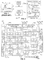
- FIG. 2 is a block diagram showing a portion of a CAM circuit according to an embodiment the present invention.
- FIG. 3 is a simplified diagram showing the CAM circuit of FIG. 2 in additional detail
- FIG. 4 is a schematic diagram showing a CAM cell of the CAM circuit shown in FIG. 3 in accordance with a first specific embodiment of the present invention
- FIGS. 5 (A) through 5 (F) are timing diagrams depicting simplified operations of a memory portion of the CAM cell shown in FIG. 4;
- FIGS. 6 (A) through 6 (D) are timing diagrams depicting simplified operations of a logic portion of the CAM cell shown in FIG. 4;
- FIG. 7 is a schematic diagram showing a CAM cell of a CAM array according to a second specific embodiment of the present invention.
- FIGS. 8 (A) and 8 (B) are timing diagrams depicting simplified bit/data line operations of the CAM cell shown in FIG. 7;
- FIG. 9 is a schematic diagram showing a CAM cell of a CAM array according to a third specific embodiment of the present invention.
- FIGS. 10 (A) through 10 (D) are timing diagrams depicting simplified bit and word line operations of the CAM cell shown in FIG. 9 .
- the present invention is described below with specific reference to binary SPAM CAM cells and ternary DRAM CAM cells. However, it is noted that the present invention can be extended to include other types of CAM cells, including ternary and quad (four-state) SEAM CAM cells, and binary and quad DRAM CAM cells. Accordingly, the specific CAM cell embodiments described herein are intended to be exemplary, and not limiting (unless otherwise specified in the claims).
- FIG. 2 is a block diagram showing part of a CAM circuit 200 including a simplified CAM cell 100 .
- CAM cell 100 is divided for descriptive purposes into a memory portion 110 and a logic portion 120 that are fabricated using known fabrication (e.g., CMOS) techniques.
- Memory portion 110 includes a memory cell 111 that is controlled by a word line WL to store a data value transmitted on a bit line B during a write operation, and transmits the stored data value SD from a storage node N 1 to logic circuit 120 during compare operations.
- Logic circuit 120 includes a comparator 121 that receives stored data value SD at a first terminal T 1 , and compares stored data value SD with an applied data value AD transmitted on a data line D and received at a second terminal T 2 .
- Icomparator 121 opens a path between a pre-charged match line MATCH and a discharge line LM, thereby causing a previously applied charge on the match line to discharge.
- stored data value SD is the same as applied data value AD (e.g., both SD and AD are logic “1”)
- the path between match line MATCH and discharge line LM remains closed, thereby maintaining the pre-charge on match line MATCH.
- the match line may be charged instead of discharged in response to the no-match condition, or may be discharged in response to a match condition.
- CAM circuit 200 also includes a memory control circuit 130 for controlling memory cell 111 of CAM cell 100 , and a logic control circuit 140 for controlling logic portion 120 of CAM cell 100 .
- memory control circuit 130 controls memory cell 100 such that storage node N 1 is selectively coupled to a relatively high memory (first) operating voltage VCCM (e.g., when a logic “1” is written to memory cell 111 ) such that a charge stored at memory cell 111 has a relatively high value.
- first operating voltage VCCM e.g., when memory cell 111 is an SRAM cell
- memory control circuit 130 includes a voltage source that latches storage node N 1 to memory operating voltage VCCM during a logic “1” write operation.
- memory control circuit 130 when memory cell 111 is a DRAM cell, memory control circuit 130 includes a bit line control circuit that transmits memory operating voltage V CCM to storage node N 1 during a logic “1” write operation. These examples are described in additional detail below. Similar to the memory control circuit, logic control circuit 140 couples the match lines (i.e., MATCH and LM) to a logic (second) operating voltage V CCL before each compare operation, and selectively transmits either logic operating voltage V CCL (e.g., logic “1”), or the low voltage V SS (e.g., logic “0”) onto data line D and in accordance with the operations described below.
- logic operating voltage is used herein to refer to the most-positive (maximum) voltage level applied to the associated portion of CAM cell 100 .
- memory operating voltage V CCM is greater than logic operating voltage V CCL , thereby providing a CAM circuit that both resists the “soft error” discharge event described above with reference to FIG. 1, and minimizes power consumption of the CAM circuit.
- the higher memory operating voltage V CCM provides a relatively high charge stored at storage node N 1 of data memory cell 111 , thereby resisting “soft error” discharges by increasing the capacitance at storage node N 1 , while the lower logic operating voltage V CCL facilitates lower power consumption by logic portion 120 during compare operations.
- memory operating voltage V CCM is greater than logic operating voltage V CCL .
- memory operating voltage V CCM is 2.5 Volts
- logic operating voltage V CCL is 1.2 to 1.5 Volts, although a smaller difference may provide beneficial performance.
- Memory control circuit 130 and logic control circuit 140 are constructed according to known techniques.
- FIG. 3 is a schematic diagram showing CAM circuit 200 in additional detail.
- CAM circuit including CAM cells (CC) 100 ( 0 , 0 ) through 100 ( 3 , 3 ) that are arranged in rows and columns.
- Each CAM cell 100 ( 0 , 0 ) through 100 ( 3 , 3 ) is essentially identical to CAM cell 100 (see FIG. 2 ).
- Each column of CAM cells e.g., cells 100 ( 0 , 0 ) through 100 ( 3 , 0 )
- is connected to an associated data line e.g., data line D 1
- an associated bit line e.g., bit line B 1
- the bit lines are used to transmit data values to the data memory cells (i.e., data memory cell 111 ; see FIG. 2) of each CAM cell in the associated column during data write operations.
- the data lines are used to transmit applied data values to the logic circuit (i.e., comparator 121 see FIG. 2) of each CAM cell in the associated column during comparison operations.
- each row of CAM cells e.g., cells 100 ( 0 , 0 ) through 100 ( 0 , 3 )
- an associated match line e.g., data line MATCH 1
- an associated low match (discharge) line e.g., low match line LM 1
- an associated word line e.g., low match line W 1
- the word lines are used to address the data memory cells of each CAM cell in the associated row during data write operations.
- the match line associated with each row of CAM cells is discharged to the associated low match line in the manner described above when any of the CAM cells in the row detect a no-match condition between the applied data value on the associated data line and the stored (first) data value in that CAM cell.
- any CAM cell in a given row e.g., any of CAM cells 100 ( 0 , 0 ), 100 ( 0 , 1 ), 100 ( 0 , 2 ), and 100 ( 0 , 3 )
- the associated match line e.g., match line MATCH 1
- the associated low match line e.g., low match line LM 1
- sixteen CAM cells are used in the present embodiment for descriptive purposes, and actual CAM arrays typically include several thousand CAM cells.
- additional circuitry associated with CAM circuit 200 e.g., input/output circuitry is omitted from the simplified description for brevity. Note that this-additional circuitry can either by driven using the relatively high memory operating voltage V CCM , or by the relatively low logic operating voltage V CCL .
- CAM circuit 200 also includes a memory control circuit 130 and a logic control circuit 140 .
- logic control circuit 140 includes a first portion 140 A, which includes a match line control circuit 210 , a low match control circuit 220 , and a data line control circuit 240 , and a second portion 140 B, which includes a priority encoder circuit 270 .
- memory control circuit 130 includes a first portion 130 A including a bit line control circuit 250 and a word line control circuit 260 , and a second portion 130 B including an optional voltage source 280 .
- memory control circuit portion 130 A is either driven using relatively high memory operating voltage V CCM , or using the relatively low logic operating voltage V CCL .
- Bit line control circuit 250 transmits data signals to selected bit lines (e.g., data line B 1 ) during data write operations.
- these data signals can either be memory operating voltage V CCM or logic operating voltage V CCL , when the transmitted data values is, for example logic “1”, or ground (V SS ) when the transmitted data value is, for example, logic “0”.
- these data signals must be memory operating voltage V CCM when the transmitted data values is, for example logic “1”, and ground (V SS ) when the transmitted data value is, for example, logic “0”.
- word line control circuit 260 transmits address signals to selected word lines (e.g., word line W 1 ) during data write operations. Similar to bit line control circuit 250 , the signals generated by word line control circuit 260 can either be memory operating voltage V CCM or logic operating voltage V CCL , when the transmitted data values is, for example logic “1”, or ground (V SS ) when the transmitted data value is, for example, logic “0”.
- optional voltage source 280 (memory control circuit portion 130 B) is used in SRAM-based embodiments, and applies memory operating voltage V CCM to each CAM cell 100 ( 0 , 0 ) through 100 ( 3 , 3 ) of the CAM array in the manner described below with reference to the specific embodiments. Note that separate voltage source 280 is not needed in DRAM-based embodiments.
- storage node N 1 is coupled to memory operating voltage V CCM during write operations (i.e., when a logic “1”, is written to a selected memory cell).
- this coupling is between storage node N 1 and voltage source 280 (i.e., the SRAM cell is latched such that storage node N 1 is coupled to voltage source 280 ).
- this coupling is generated by selectively coupling storage node N 1 to bit line B, which is pulled up to memory operating voltage V CCM . Therefore, in either embodiment, a relatively high charge is stored by memory cell 111 , thereby facilitating resistance to soft error discharge.
- the memory cells 100 ( 0 , 0 ) through 100 ( 3 , 3 ) are accessed relatively independently (i.e., only one or a small group of memory cells is accessed at any given time) during, for example, write operations, the use of a relatively high memory operating voltage V CCM to drive the memory portion of CAM circuit 200 does not significantly increase power. consumption.
- each circuit of logic portion 140 is controlled using logic operating voltage V CCL .
- Match line control circuit 210 generates a pre-charge equal to logic operating voltage V CCL on each of several match lines (e.g., match line MATCH 1 ) in accordance with the comparison operation described below.
- Low match control circuit 220 controls the low match lines (e.g., low match line LM 1 ) such that they float during non-active periods, and are pulled down to a pre-determined low voltage (e.g., ground or 0 volts) during compare operations.
- a pre-determined low voltage e.g., ground or 0 volts
- low match line LM 1 may be maintained at 0 volts at all times.
- Data line control circuit 240 transmits applied data signals to selected data lines (e.g., data line D 1 ) during compare operations.
- priority encoder circuit 270 is controlled using logic operating voltage V CCL to sense and identify the charged/discharged state of the match lines during compare operations, and passes the resulting match line information to associated control circuitry (not shown). Because the logic portions of CAM cells 100 ( 0 , 0 ) through 100 ( 3 , 3 ) are accessed at the same time during compare operations, the use of the relatively low logic operating voltage V CCL to drive the logic portions of CAM circuit 200 prevents high power consumption. Accordingly, using two different operating voltages to drive the memory portions and logic portions of each CAM cell in CAM circuit 200 facilitates both a reduction in “soft error” discharge, and a reduction in the overall power consumption of the CAM circuit.
- CAM circuits will recognize that the sixteen CAM cells depicted in the embodiment shown in FIG. 3 are provided solely for descriptive purposes, and that actual CAM arrays typically include several thousand CAM cells. Further, the specific control circuits depicted in the embodiment shown in FIG. 3 are intended to be exemplary, and not limiting. For example, those familiar with CAM circuits will recognize that additional circuitry associated with the operation of CAM circuit 200 (e.g., input/output circuitry) is omitted from the simplified embodiment shown in FIG. 3 . Such circuitry is omitted from description solely for the sake of brevity. Note that such additional circuitry can either by driven using the relatively high memory operating voltage V CCM or the relatively low logic operating voltage V CCL .
- V CCM relatively high memory operating voltage
- V CCL relatively low logic operating voltage
- CAM circuit 200 The operation of CAM circuit 200 is described below with respect to specific embodiments of CAM cell 100 . Note that the disclosed specific embodiments are intended to be illustrative, and not limiting.
- FIG. 4 is a schematic diagram showing a CAM cell 100 A in accordance with a first specific embodiment of the present invention. Similar to CAM cell 100 (see FIG. 2 ), CAM cell 100 A includes an SRAM cell 111 A and a comparator 121 A. SRAM cell 111 A is connected to complementary bit lines B 1 and B 1 # (“#” is used herein to denote an inverted signal), word line WL 1 , memory operating voltage V CCM (i.e., from voltage source 280 ; see FIG. 3 ), and a (ground) V SS voltage supply source. Comparator 121 A is connected to complementary data lines D 1 and D 1 #, low match line LM 1 , and match line MATCH 1 .
- SRAM cell 111 A is connected to complementary bit lines B 1 and B 1 # (“#” is used herein to denote an inverted signal), word line WL 1 , memory operating voltage V CCM (i.e., from voltage source 280 ; see FIG. 3 ), and a (ground) V SS voltage
- SRAM cell 111 A includes p-channel transistors 411 and 412 and n-channel transistors 413 - 416 , which are fabricated according to known techniques. Transistors 411 and 413 are connected in series between the V CCM operating voltage and the V SS voltage supply source, and transistors 412 and 414 are also connected in series between V CCM and V SS . Transistors 411 and 413 and transistors 412 and 414 of SRAM cell 111 A are cross-coupled to form a storage latch.
- a first storage node N 1 # that is located between transistors 411 and 413 is connected to the gate terminals of transistors 412 and 414
- a second storage node N 1 that is located between transistors 412 and 414 is connected to the gate terminals of transistors 411 and 413
- Access transistor 415 is connected between bit line B 1 # and node N 1 #
- Access transistor 416 is connected between bit line B 1 and node N 1 .
- the gates of access transistors 415 and 416 are connected to word line WL 1 .
- SRAM cell 111 A only stores a single data value (bit) that is either a logic high value i maintained at node N 1 (i.e., node N 1 is coupled to memory voltage signal V CCM )) and a low voltage signal (V SS ) maintained at inverted node N 1 #), or a logic low value (e.g., a low voltage signal (V SS ) maintained at node N 1 and a high voltage signal (V CCM ) maintained at inverted node N 1 #)
- J comparator 121 A includes n-channel transistors 426 , 427 and 428 .
- Transistor 428 is connected between match line MATCH, and low match line LM 1 .
- Transistor 426 has a first terminal connected to data line D 1 , a gate terminal connected to inverted node N 1 #, and a second terminal connected to a node N 2 , which is connected to the gate terminal of transistor 428 .
- Transistor 427 has a first terminal connected to inverted data line D 1 #, a gate terminal connected to node N 1 , and a second terminal connected to node N 2 .
- transistor 428 is turned on to provide a path between match line MATCH 1 and low match line LM 1 when either (a) the data value stored at inverted node N 1 # and transmitted on data line D 1 are high (i.e., V CCM and V CCL , respectively), or (b) the data value stored at node N 1 and transmitted on inverted data line D 1 # are high (i.e., V CCM and V CCL , respectively). Under either of these conditions, a high voltage (i.e., V CCL ) is applied to the gate terminal of transistor 428 , thereby turning on this transistor and coupling match line MATCH 1 with low match line LM 1 .
- V CCL a high voltage
- FIGS. 5 (A) through 5 (F) depict signals generated in the memory portion of CAM cell 100 A during a time period spanning time t 0 through t 6
- FIGS. 6 (A) through 6 (D) depict signals generated in the logic portion of CAM cell 100 A during the same period.
- time t 0 to t 2 represents a standby period
- time t 2 through t 4 apply to a data write operation
- time t 4 to t 6 apply to a compare operation.
- the times indicated in these timing diagrams are simplified for descriptive purposes.
- a relatively high constant operating voltage V CCM (e.g., 2.5 Volts) is applied to the first terminals of transistors 411 and 412 . As described above with reference to FIG. 3, this constant operating voltage V CCM is transmitted to each SRAM cell from voltage supply 280 . In the present example, V SS is maintained at 0 Volts.
- word line WL 1 (FIG. 5 (D)) and-data lines D 1 and D 1 # (FIGS. 6 (C) and 6 (D), respectively) are pulled down to logic low (0 Volts) values, thereby turning off transistors 415 , 416 , and 428 .
- the signal transmitted on bit line B 1 (FIG. 5 (B)), inverted bit line B 1 # (FIG. 5 (C)), match line MATCH 1 (FIG. 6 (A)), and low match line LM 1 (FIG. 6 (B)) does not matter (i.e., can be either high or low).
- the value stored at node N 1 (FIG. 5 (E)) and inverted node N 1 # (FIG. 5 (F)) does not matter.
- bit line B 1 is maintained at either memory operating voltage V CCM (2.5 Volts) or logic operating voltage V CCL (e.g., 1.2 Volts) during the write operation. Note that either of operating voltages V CCM or V CCL may be utilized, and the selection of either operating voltage is based, for example, on circuit design convenience.
- inverted bit line B 1 # is maintained at V SS throughout the write operation. Referring to FIG.
- word line WL 1 is pulled up to V CCM (or V CCL ) to turn on transistors 415 and 416 , thereby passing the logic values from bit lines B 1 # and B 1 , respectively, to the latch formed by transistors 411 - 414 .
- this write operation causes the latch to maintain a logic high or V CCM value (2.5 Volts) at node N 1 , and a logic low or V CCM value (0 Volts) at inverted node N 1 #. Note that data lines D 1 and D 1 # (FIGS.
- bit line B 1 is held to a logic low value and bit line B 1 # is held to a logic high value when word line WL 1 turns on transistors 115 and 116 , thereby pulling up inverted node N 1 # to a logic high value and pulling down node N 1 to a logic low value in a manner similar to that described above.
- a compare operation (time t 4 to t 6 ) will now be described during which a logic “0” (i.e., low) data value is applied to comparator 121 A between.
- V CCL logic operating voltage
- Both low match line LM 1 (FIG. 6 (B) and word line WL 1 (FIG. 5 (D) are held at logic low values at this time.
- the data values on bit lines B 1 and B 1 # (FIGS. 5 (B) and 5 (C)) are not utilized in the compare operation, and are therefore left in their previous states.
- a “match” condition is indicated during a compare operation when a high logic value is maintained on match line MATCH 1
- a no-match condition is indicated during a compare operation when match line MATCH 1 is discharged.
- a high logic value e.g., 1.5 Volts
- a low logic value is applied to data line D 1 (FIGS. 6 (D) and 6 (C), respectively).
- the high logic value on inverted data line D 1 # is passed by transistor 427 , which is turned on by the high data value stored at node N 1 .
- transistor 428 is turned on during a compare operation to open a discharge path between match line MATCH 1 and low match line LM 1 , which is indicated by the low match line signal at time t 5 (FIG. 6 (A)). Note that if a logic 1 were applied on data lines D 1 and D 1 #, the resulting low value passed by transistor 427 would not turn on transistor 428 , and match line MATCH 1 would remain at V CCL .
- FIG. 7 is a schematic diagram showing a CAM cell 100 B in accordance with a second specific embodiment of the present invention.
- CAM cell 100 B includes SRAM cell 111 A, which is described above with reference to FIG. 4, and a comparator 121 B that operates as described below.
- comparator 121 B In addition to the different circuit structure provided by comparator 121 B, CAM cell 100 B differs from CAM cell 100 A in that, instead of separate bit lines and data lines, a single pair of bit/data lines B/D# and B#/D are used to transmit data signals during both write and compare operations, as described below.
- comparator 121 B includes n-channel transistors 721 - 724 .
- Transistors 721 and 723 are connected in series between match line MATCH 1 and low match line LM 1
- transistors 722 and 724 are also connected in series between match line MATCH 1 and low match line LM 1 .
- the gate terminal of transistor 721 is connected to bit/data line B#/D 1 and the gate terminal of transistor 723 is connected to node N 1 #. Therefore, during compare operations, transistors 721 and 723 are turned on to open a first path between match line MATCH 1 and low match line LM 1 only when a high applied data signal is transmitted on bit/data line B#/D and a high data signal is stored at node N 1 #.
- transistor 722 is connected to bit/data line B/D#
- the gate terminal of transistor 724 is connected to node N 1 . Therefore, transistors 722 and 724 are turned on to open a second path between match line MATCH 1 and low match line LM 1 only when a high applied data signal is transmitted on bit/data line B/D# and a high data signal is stored at node N 1 .
- shared bit/data lines B#/D and B/D# are controlled using either the higher memory or lower logic operating voltages (i.e., either V CCM or V CCL ) during memory operations, and using the logic operating voltage (i.e., V CCL ) during logic (e.g., compare) operations.
- a high operating voltage e.g., either 1.2 or 2.5 Volts
- bit/data line B/D# shown using dashed lines in FIG.
- bit/data line B#/D (shown in FIG. 8 (B)) between time t 2 and t 4 , and a low voltage (e.g., 0 Volts) is transmitted on bit/data line B#/D (shown in FIG. 8 (B)).
- a low voltage e.g., 0 Volts
- bit/data line B#/D shown in FIG. 8 (B)
- word line WL 1 when word line WL 1 is subsequently turned on, the operating voltage transmitted on bit/data line B/D# is passed to the latch formed by transistors 411 through 414 of SRAM cell 111 A, thereby storing a high data signal at node N 1 and a low data signal at inverted node N 1 #.
- a relatively low operating voltage e.g. 1.5 Volts
- a relatively low voltage e.g. 1.5 Volts
- a low voltage e.g., 0 Volts
- the match line is controlled using the relatively low logic operating voltage V CCL . Similar to the example described above with reference to FIGS.
- CAM cell 100 B is similar to that of CAM cell 100 A (described above), but a CAM circuit incorporating an array of CAM cells 100 B can be made smaller than a CAM circuit using CAM cells 100 A because memory and logic operations are performed using a single pair of complementary bit/data lines, instead of the four lines used to operate CAM cell 100 A.
- FIG. 9 is a schematic diagram showing a portion of a ternary DRAM-based CAM circuit includes an array of ternary CAM cells 100 C (one shown) that is formed and operated in accordance with a third specific embodiment of the present invention.
- CAM cell 100 C includes a first one-transistor ( 1 T) DRAM cell 811 A, a second 1 T DRAM cell 811 B, and logic circuit 121 B (described above with reference to FIG. 7 ).
- DRAM cell 811 A includes transistor Q 1 and a capacitor structure C 1 , which combine to form a storage node N 1 that receives a data value from bit line BL 1 during write operations, and applies the stored data value to the gate terminal of transistor 723 of comparator circuit 121 B.
- DRAM cell 811 B includes transistor Q 2 and a capacitor structure C 2 , which combine to form a storage node N 1 # that receives a data value from bit line BL 2 , and applies the stored data value to the gate terminal of transistor 724 of comparator circuit 121 B.
- CAM cell 100 C The operation of CAM cell 100 C is similar to that described above, with the exception that a “don't care” state is stored when both DRAM cells 811 A and 811 B store logic low data values, thereby preventing discharge of match line MATCH 1 no matter what data values are transmitted on data lines D 1 and D 1 #.
- DRAM cells 811 A and 811 B are not coupled to an independent voltage source, as in the SRAM-based examples provided above, logic “1” data signals are transmitted to and stored in DRAM cells 811 A and 811 B by maintaining bit line BL 1 or BL 2 (depending on the data value being written) at memory voltage source V CCM (e.g., 2.5 Volts) during the write operation, and then turning on word lines WL 1 and WL 2 , also using memory voltage source V CCM .
- V CCM e.g. 2.5 Volts
- bit line BL 1 is pulled up to memory voltage source V CCM at time t 2 (bit line BL 2 is maintained at V SS ), and word lines WL 1 and WL 2 are pulled up to memory voltage V CCM at time t 3 , thereby transferring voltage V CCM to storage node N 1 .
- the relatively high stored voltage V CCM facilitates resistance to soft error discharge.
- data lines D 1 and D 1 #, match line MATCH 1 and low match line LM 1 are driven using logic voltage source V CCL .
- the present invention is described with reference to certain binary SRAM CAM cells and ternary DRAM CAM cells, several alternative embodiments also fall within the spirit and scope of the invention.
- the four-transistor comparator 121 B (FIGS. 7 and 9) can be utilized in place of the three-transistor comparator 121 A of CAM cell 100 A (FIG. 4 ).
- the three-transistor comparator 121 A (FIG. 4) can be utilized in place of the four-transistor comparator 121 B of CAM cells 100 B and 100 C (FIGS. 7 and 9 ).
- the SRAM CAM circuits disclosed herein can be modified to include ternary and quad (four-state) SRAM CAM cells by including one or more additional SRAM cells in each CAM cell according to known techniques.
- the DRAM CAM circuit disclosed herein can be modified to implement a binary or and quad DRAM CAM cells. In view of these and other possible modifications, the invention is limited only by the following claims.
Abstract
Description
Claims (20)
Priority Applications (2)
| Application Number | Priority Date | Filing Date | Title |
|---|---|---|---|
| US10/164,981 US6512685B1 (en) | 2002-06-06 | 2002-06-06 | CAM circuit with separate memory and logic operating voltages |
| US10/350,991 US6661687B1 (en) | 2002-06-06 | 2003-01-23 | Cam circuit with separate memory and logic operating voltages |
Applications Claiming Priority (1)
| Application Number | Priority Date | Filing Date | Title |
|---|---|---|---|
| US10/164,981 US6512685B1 (en) | 2002-06-06 | 2002-06-06 | CAM circuit with separate memory and logic operating voltages |
Related Child Applications (1)
| Application Number | Title | Priority Date | Filing Date |
|---|---|---|---|
| US10/350,991 Continuation-In-Part US6661687B1 (en) | 2002-06-06 | 2003-01-23 | Cam circuit with separate memory and logic operating voltages |
Publications (1)
| Publication Number | Publication Date |
|---|---|
| US6512685B1 true US6512685B1 (en) | 2003-01-28 |
Family
ID=22596906
Family Applications (2)
| Application Number | Title | Priority Date | Filing Date |
|---|---|---|---|
| US10/164,981 Expired - Lifetime US6512685B1 (en) | 2002-06-06 | 2002-06-06 | CAM circuit with separate memory and logic operating voltages |
| US10/350,991 Expired - Lifetime US6661687B1 (en) | 2002-06-06 | 2003-01-23 | Cam circuit with separate memory and logic operating voltages |
Family Applications After (1)
| Application Number | Title | Priority Date | Filing Date |
|---|---|---|---|
| US10/350,991 Expired - Lifetime US6661687B1 (en) | 2002-06-06 | 2003-01-23 | Cam circuit with separate memory and logic operating voltages |
Country Status (1)
| Country | Link |
|---|---|
| US (2) | US6512685B1 (en) |
Cited By (10)
| Publication number | Priority date | Publication date | Assignee | Title |
|---|---|---|---|---|
| US6618281B1 (en) * | 2002-05-15 | 2003-09-09 | International Business Machines Corporation | Content addressable memory (CAM) with error checking and correction (ECC) capability |
| US20030227788A1 (en) * | 2002-06-06 | 2003-12-11 | Integrated Device Technology, Inc. | CAM circuit with radiation resistance |
| US20040037104A1 (en) * | 2002-08-21 | 2004-02-26 | Loughmiller Daniel R. | High density dynamic ternary-CAM memory architecture |
| US20040208034A1 (en) * | 2002-06-06 | 2004-10-21 | Integrated Device Technology, Inc. | CAM circuit with radiation resistance |
| US20040252572A1 (en) * | 2003-06-11 | 2004-12-16 | Artisan Components, Inc. | Method and apparatus for reducing write power consumption in random access memories |
| US6867989B1 (en) * | 2002-07-29 | 2005-03-15 | Netlogic Microsystems, Inc. | Auto read content addressable memory cell and array |
| US20070165436A1 (en) * | 2004-07-19 | 2007-07-19 | Vishal Sarin | High-speed and low-power differential non-volatile content addressable memory cell and array |
| US20120127804A1 (en) * | 2010-11-18 | 2012-05-24 | Grandis, Inc. | Memory Write Error Correction Circuit |
| US9001545B2 (en) | 2012-08-31 | 2015-04-07 | Aplus Flash Technology, Inc. | NOR-based BCAM/TCAM cell and array with NAND scalability |
| CN109727625A (en) * | 2017-10-27 | 2019-05-07 | 三星电子株式会社 | According to the memory devices of priority driven matched line |
Families Citing this family (11)
| Publication number | Priority date | Publication date | Assignee | Title |
|---|---|---|---|---|
| US6529395B1 (en) * | 2001-11-15 | 2003-03-04 | Broadcom Corporation | Content addressable memory cell techniques |
| US7301961B1 (en) | 2001-12-27 | 2007-11-27 | Cypress Semiconductor Corportion | Method and apparatus for configuring signal lines according to idle codes |
| US6751110B2 (en) * | 2002-03-08 | 2004-06-15 | Micron Technology, Inc. | Static content addressable memory cell |
| US6987684B1 (en) | 2003-07-15 | 2006-01-17 | Integrated Device Technology, Inc. | Content addressable memory (CAM) devices having multi-block error detection logic and entry selective error correction logic therein |
| US7193876B1 (en) | 2003-07-15 | 2007-03-20 | Kee Park | Content addressable memory (CAM) arrays having memory cells therein with different susceptibilities to soft errors |
| US7304875B1 (en) | 2003-12-17 | 2007-12-04 | Integrated Device Technology. Inc. | Content addressable memory (CAM) devices that support background BIST and BISR operations and methods of operating same |
| US7120040B2 (en) * | 2004-06-01 | 2006-10-10 | Mosaid Technologies Incorporation | Ternary CAM cell for reduced matchline capacitance |
| US7324362B1 (en) * | 2005-03-01 | 2008-01-29 | Netlogic Microsystems Inc. | Content addressable memory cell configurable between multiple modes and method therefor |
| US7355905B2 (en) | 2005-07-01 | 2008-04-08 | P.A. Semi, Inc. | Integrated circuit with separate supply voltage for memory that is different from logic circuit supply voltage |
| US7586780B2 (en) * | 2006-12-18 | 2009-09-08 | Panasonic Corporation | Semiconductor memory device |
| US8638582B1 (en) * | 2011-08-23 | 2014-01-28 | Netlogic Microsystems, Inc. | Content addressable memory with base-three numeral system |
Citations (13)
| Publication number | Priority date | Publication date | Assignee | Title |
|---|---|---|---|---|
| US4506436A (en) | 1981-12-21 | 1985-03-26 | International Business Machines Corporation | Method for increasing the radiation resistance of charge storage semiconductor devices |
| US4779226A (en) | 1985-05-10 | 1988-10-18 | Haraszti Tegze P | Complementary high performance cam cell |
| US4791606A (en) | 1987-09-01 | 1988-12-13 | Triad Semiconductors International Bv | High density CMOS dynamic CAM cell |
| US4876215A (en) | 1987-07-02 | 1989-10-24 | Integrated Device Technology, Inc. | Method of making a static ram cell with trench pull-down transistors and buried-layer ground plate |
| US5483479A (en) * | 1992-04-22 | 1996-01-09 | Mitsubishi Denki Kabushiki Kaisha | Associative storage memory |
| US5561429A (en) | 1986-04-16 | 1996-10-01 | Raytheon Company | Content limit addressable memory |
| US5572460A (en) | 1993-10-26 | 1996-11-05 | Integrated Device Technology, Inc. | Static random-access memory cell with capacitive coupling to reduce sensitivity to radiation |
| US5681769A (en) | 1994-09-06 | 1997-10-28 | Integrated Device Technology, Inc. | Method of fabricating a high capacitance insulated-gate field effect transistor |
| US5740097A (en) * | 1994-11-28 | 1998-04-14 | International Business Machines Corporation | Content-addressable-memory control circuit |
| US5901085A (en) * | 1996-09-30 | 1999-05-04 | Stmicroelectronics, S.R.L. | Programmable reference voltage source, particularly for analog memories |
| US6005790A (en) * | 1998-12-22 | 1999-12-21 | Stmicroelectronics, Inc. | Floating gate content addressable memory |
| US6067656A (en) | 1997-12-05 | 2000-05-23 | Intel Corporation | Method and apparatus for detecting soft errors in content addressable memory arrays |
| US6146936A (en) | 1997-08-22 | 2000-11-14 | Micron Technology, Inc. | Integrated circuitry, methods of reducing alpha particle inflicted damage to SRAM cells, methods of forming integrated circuitry, and methods of forming SRAM cells |
Family Cites Families (5)
| Publication number | Priority date | Publication date | Assignee | Title |
|---|---|---|---|---|
| JP3190868B2 (en) * | 1997-11-21 | 2001-07-23 | エヌイーシーマイクロシステム株式会社 | Associative memory device |
| US6128207A (en) | 1998-11-02 | 2000-10-03 | Integrated Device Technology, Inc. | Low-power content addressable memory cell |
| US6081440A (en) * | 1998-11-05 | 2000-06-27 | Lara Technology, Inc. | Ternary content addressable memory (CAM) having fast insertion and deletion of data values |
| US6101116A (en) * | 1999-06-30 | 2000-08-08 | Integrated Device Technology, Inc. | Six transistor content addressable memory cell |
| US6154384A (en) * | 1999-11-12 | 2000-11-28 | Netlogic Microsystems, Inc. | Ternary content addressable memory cell |
-
2002
- 2002-06-06 US US10/164,981 patent/US6512685B1/en not_active Expired - Lifetime
-
2003
- 2003-01-23 US US10/350,991 patent/US6661687B1/en not_active Expired - Lifetime
Patent Citations (13)
| Publication number | Priority date | Publication date | Assignee | Title |
|---|---|---|---|---|
| US4506436A (en) | 1981-12-21 | 1985-03-26 | International Business Machines Corporation | Method for increasing the radiation resistance of charge storage semiconductor devices |
| US4779226A (en) | 1985-05-10 | 1988-10-18 | Haraszti Tegze P | Complementary high performance cam cell |
| US5561429A (en) | 1986-04-16 | 1996-10-01 | Raytheon Company | Content limit addressable memory |
| US4876215A (en) | 1987-07-02 | 1989-10-24 | Integrated Device Technology, Inc. | Method of making a static ram cell with trench pull-down transistors and buried-layer ground plate |
| US4791606A (en) | 1987-09-01 | 1988-12-13 | Triad Semiconductors International Bv | High density CMOS dynamic CAM cell |
| US5483479A (en) * | 1992-04-22 | 1996-01-09 | Mitsubishi Denki Kabushiki Kaisha | Associative storage memory |
| US5572460A (en) | 1993-10-26 | 1996-11-05 | Integrated Device Technology, Inc. | Static random-access memory cell with capacitive coupling to reduce sensitivity to radiation |
| US5681769A (en) | 1994-09-06 | 1997-10-28 | Integrated Device Technology, Inc. | Method of fabricating a high capacitance insulated-gate field effect transistor |
| US5740097A (en) * | 1994-11-28 | 1998-04-14 | International Business Machines Corporation | Content-addressable-memory control circuit |
| US5901085A (en) * | 1996-09-30 | 1999-05-04 | Stmicroelectronics, S.R.L. | Programmable reference voltage source, particularly for analog memories |
| US6146936A (en) | 1997-08-22 | 2000-11-14 | Micron Technology, Inc. | Integrated circuitry, methods of reducing alpha particle inflicted damage to SRAM cells, methods of forming integrated circuitry, and methods of forming SRAM cells |
| US6067656A (en) | 1997-12-05 | 2000-05-23 | Intel Corporation | Method and apparatus for detecting soft errors in content addressable memory arrays |
| US6005790A (en) * | 1998-12-22 | 1999-12-21 | Stmicroelectronics, Inc. | Floating gate content addressable memory |
Cited By (20)
| Publication number | Priority date | Publication date | Assignee | Title |
|---|---|---|---|---|
| WO2003098633A3 (en) * | 2002-05-15 | 2004-05-06 | Ibm | Content addressable memory (cam) with error checking and correction |
| US6618281B1 (en) * | 2002-05-15 | 2003-09-09 | International Business Machines Corporation | Content addressable memory (CAM) with error checking and correction (ECC) capability |
| US20040208034A1 (en) * | 2002-06-06 | 2004-10-21 | Integrated Device Technology, Inc. | CAM circuit with radiation resistance |
| US20030227788A1 (en) * | 2002-06-06 | 2003-12-11 | Integrated Device Technology, Inc. | CAM circuit with radiation resistance |
| US6924995B2 (en) | 2002-06-06 | 2005-08-02 | Integrated Device Technology, Inc. | CAM circuit with radiation resistance |
| US6754093B2 (en) * | 2002-06-06 | 2004-06-22 | Integrated Device Technology, Inc. | CAM circuit with radiation resistance |
| US6867989B1 (en) * | 2002-07-29 | 2005-03-15 | Netlogic Microsystems, Inc. | Auto read content addressable memory cell and array |
| US20040196701A1 (en) * | 2002-08-21 | 2004-10-07 | Loughmiller Daniel R. | High density dynamic ternary-CAM memory architecture |
| US6847534B2 (en) | 2002-08-21 | 2005-01-25 | Micron Technology, Inc. | High density dynamic ternary-CAM memory architecture |
| US6744654B2 (en) * | 2002-08-21 | 2004-06-01 | Micron Technology, Inc. | High density dynamic ternary-CAM memory architecture |
| US20040037104A1 (en) * | 2002-08-21 | 2004-02-26 | Loughmiller Daniel R. | High density dynamic ternary-CAM memory architecture |
| US20040252572A1 (en) * | 2003-06-11 | 2004-12-16 | Artisan Components, Inc. | Method and apparatus for reducing write power consumption in random access memories |
| US6934213B2 (en) * | 2003-06-11 | 2005-08-23 | Artisan Components, Inc. | Method and apparatus for reducing write power consumption in random access memories |
| US20070165436A1 (en) * | 2004-07-19 | 2007-07-19 | Vishal Sarin | High-speed and low-power differential non-volatile content addressable memory cell and array |
| US7423895B2 (en) * | 2004-07-19 | 2008-09-09 | Silicon Storage Technology, Inc. | High-speed and low-power differential non-volatile content addressable memory cell and array |
| US20120127804A1 (en) * | 2010-11-18 | 2012-05-24 | Grandis, Inc. | Memory Write Error Correction Circuit |
| US8456926B2 (en) * | 2010-11-18 | 2013-06-04 | Grandis, Inc. | Memory write error correction circuit |
| US9001545B2 (en) | 2012-08-31 | 2015-04-07 | Aplus Flash Technology, Inc. | NOR-based BCAM/TCAM cell and array with NAND scalability |
| CN109727625A (en) * | 2017-10-27 | 2019-05-07 | 三星电子株式会社 | According to the memory devices of priority driven matched line |
| CN109727625B (en) * | 2017-10-27 | 2024-03-12 | 三星电子株式会社 | Memory device for driving match lines according to priority |
Also Published As
| Publication number | Publication date |
|---|---|
| US6661687B1 (en) | 2003-12-09 |
| US20030227789A1 (en) | 2003-12-11 |
Similar Documents
| Publication | Publication Date | Title |
|---|---|---|
| US6512685B1 (en) | CAM circuit with separate memory and logic operating voltages | |
| US5881010A (en) | Multiple transistor dynamic random access memory array architecture with simultaneous refresh of multiple memory cells during a read operation | |
| US6560156B2 (en) | CAM circuit with radiation resistance | |
| US8072797B2 (en) | SRAM cell without dedicated access transistors | |
| US7502273B2 (en) | Two-port SRAM with a high speed sensing scheme | |
| US8654575B2 (en) | Disturb-free static random access memory cell | |
| US7821858B2 (en) | eDRAM hierarchical differential sense AMP | |
| US7643357B2 (en) | System and method for integrating dynamic leakage reduction with write-assisted SRAM architecture | |
| US7643329B2 (en) | Asymmetric four-transistor SRAM cell | |
| US6738283B2 (en) | Method of reading stored data and semiconductor memory device | |
| US7259986B2 (en) | Circuits and methods for providing low voltage, high performance register files | |
| US7269055B2 (en) | SRAM device with reduced leakage current | |
| US20040105299A1 (en) | Storage array such as a SRAM with reduced power requirements | |
| US6373739B1 (en) | Quad CAM cell with minimum cell size | |
| US7633784B2 (en) | Junction field effect dynamic random access memory cell and content addressable memory cell | |
| US7872938B2 (en) | Soft error robust static random access memory cell storage configuration. | |
| US6853579B1 (en) | Non-refresh four-transistor memory cell | |
| US6754093B2 (en) | CAM circuit with radiation resistance | |
| US20030072171A1 (en) | Content addressable memory device | |
| US6924995B2 (en) | CAM circuit with radiation resistance | |
| US7709299B2 (en) | Hierarchical 2T-DRAM with self-timed sensing | |
| US8670281B2 (en) | Circuit for memory cell recovery | |
| US6584002B1 (en) | Method of querying a four-transistor memory array as a content addressable memory by rows or columns | |
| US6226216B1 (en) | Sectional column activated memory |
Legal Events
| Date | Code | Title | Description |
|---|---|---|---|
| AS | Assignment |
Owner name: INTEGRATED DEVICE TECHNOLOGY, INC., CALIFORNIA Free format text: ASSIGNMENT OF ASSIGNORS INTEREST;ASSIGNORS:LIEN, CHUEN-DER;WU, CHAU-CHIN;REEL/FRAME:013003/0806 Effective date: 20020606 |
|
| STCF | Information on status: patent grant |
Free format text: PATENTED CASE |
|
| REMI | Maintenance fee reminder mailed | ||
| FPAY | Fee payment |
Year of fee payment: 4 |
|
| SULP | Surcharge for late payment | ||
| AS | Assignment |
Owner name: SILICON VALLEY BANK, CALIFORNIA Free format text: SECURITY AGREEMENT;ASSIGNORS:NETLOGIC MICROSYSTEMS, INC.;NETLOGIC MICROSYSTEMS INTERNATIONAL LIMITED;NETLOGIC MICROSYSTEMS CAYMANS LIMITED;REEL/FRAME:022973/0710 Effective date: 20090717 Owner name: SILICON VALLEY BANK,CALIFORNIA Free format text: SECURITY AGREEMENT;ASSIGNORS:NETLOGIC MICROSYSTEMS, INC.;NETLOGIC MICROSYSTEMS INTERNATIONAL LIMITED;NETLOGIC MICROSYSTEMS CAYMANS LIMITED;REEL/FRAME:022973/0710 Effective date: 20090717 |
|
| AS | Assignment |
Owner name: NETLOGIC MICROSYSTEMS, INC., CALIFORNIA Free format text: ASSIGNMENT OF ASSIGNORS INTEREST;ASSIGNOR:INTEGRATED DEVICE TECHNOLOGY, INC.;REEL/FRAME:022980/0624 Effective date: 20090717 |
|
| FEPP | Fee payment procedure |
Free format text: PAYOR NUMBER ASSIGNED (ORIGINAL EVENT CODE: ASPN); ENTITY STATUS OF PATENT OWNER: LARGE ENTITY Free format text: PAYER NUMBER DE-ASSIGNED (ORIGINAL EVENT CODE: RMPN); ENTITY STATUS OF PATENT OWNER: LARGE ENTITY |
|
| FPAY | Fee payment |
Year of fee payment: 8 |
|
| AS | Assignment |
Owner name: NETLOGIC MICROSYSTEMS INTERNATIONAL LIMITED, CALIF Free format text: RELEASE BY SECURED PARTY;ASSIGNOR:SILICON VALLEY BANK;REEL/FRAME:026830/0141 Effective date: 20110826 Owner name: NETLOGIC MICROSYSTEMS, INC., CALIFORNIA Free format text: RELEASE BY SECURED PARTY;ASSIGNOR:SILICON VALLEY BANK;REEL/FRAME:026830/0141 Effective date: 20110826 Owner name: NETLOGIC MICROSYSTEMS CAYMANS LIMITED, CALIFORNIA Free format text: RELEASE BY SECURED PARTY;ASSIGNOR:SILICON VALLEY BANK;REEL/FRAME:026830/0141 Effective date: 20110826 |
|
| FPAY | Fee payment |
Year of fee payment: 12 |
|
| AS | Assignment |
Owner name: BROADCOM CORPORATION, CALIFORNIA Free format text: ASSIGNMENT OF ASSIGNORS INTEREST;ASSIGNOR:NETLOGIC I LLC;REEL/FRAME:035443/0763 Effective date: 20150327 Owner name: NETLOGIC I LLC, DELAWARE Free format text: CHANGE OF NAME;ASSIGNOR:NETLOGIC MICROSYSTEMS, INC.;REEL/FRAME:035443/0824 Effective date: 20130123 |
|
| AS | Assignment |
Owner name: BANK OF AMERICA, N.A., AS COLLATERAL AGENT, NORTH CAROLINA Free format text: PATENT SECURITY AGREEMENT;ASSIGNOR:BROADCOM CORPORATION;REEL/FRAME:037806/0001 Effective date: 20160201 Owner name: BANK OF AMERICA, N.A., AS COLLATERAL AGENT, NORTH Free format text: PATENT SECURITY AGREEMENT;ASSIGNOR:BROADCOM CORPORATION;REEL/FRAME:037806/0001 Effective date: 20160201 |
|
| AS | Assignment |
Owner name: AVAGO TECHNOLOGIES GENERAL IP (SINGAPORE) PTE. LTD., SINGAPORE Free format text: ASSIGNMENT OF ASSIGNORS INTEREST;ASSIGNOR:BROADCOM CORPORATION;REEL/FRAME:041706/0001 Effective date: 20170120 Owner name: AVAGO TECHNOLOGIES GENERAL IP (SINGAPORE) PTE. LTD Free format text: ASSIGNMENT OF ASSIGNORS INTEREST;ASSIGNOR:BROADCOM CORPORATION;REEL/FRAME:041706/0001 Effective date: 20170120 |
|
| AS | Assignment |
Owner name: BROADCOM CORPORATION, CALIFORNIA Free format text: TERMINATION AND RELEASE OF SECURITY INTEREST IN PATENTS;ASSIGNOR:BANK OF AMERICA, N.A., AS COLLATERAL AGENT;REEL/FRAME:041712/0001 Effective date: 20170119 |
|
| AS | Assignment |
Owner name: AVAGO TECHNOLOGIES INTERNATIONAL SALES PTE. LIMITE Free format text: MERGER;ASSIGNOR:AVAGO TECHNOLOGIES GENERAL IP (SINGAPORE) PTE. LTD.;REEL/FRAME:047195/0026 Effective date: 20180509 |
|
| AS | Assignment |
Owner name: AVAGO TECHNOLOGIES INTERNATIONAL SALES PTE. LIMITE Free format text: CORRECTIVE ASSIGNMENT TO CORRECT THE EFFECTIVE DATE OF MERGER PREVIOUSLY RECORDED ON REEL 047195 FRAME 0026. ASSIGNOR(S) HEREBY CONFIRMS THE MERGER;ASSIGNOR:AVAGO TECHNOLOGIES GENERAL IP (SINGAPORE) PTE. LTD.;REEL/FRAME:047477/0423 Effective date: 20180905 |