US6430683B1 - Processor and method for just-in-time delivery of load data via time dependency field - Google Patents
Processor and method for just-in-time delivery of load data via time dependency field Download PDFInfo
- Publication number
- US6430683B1 US6430683B1 US09/344,023 US34402399A US6430683B1 US 6430683 B1 US6430683 B1 US 6430683B1 US 34402399 A US34402399 A US 34402399A US 6430683 B1 US6430683 B1 US 6430683B1
- Authority
- US
- United States
- Prior art keywords
- data
- dod
- time
- load
- cache
- Prior art date
- Legal status (The legal status is an assumption and is not a legal conclusion. Google has not performed a legal analysis and makes no representation as to the accuracy of the status listed.)
- Expired - Fee Related
Links
- 238000000034 method Methods 0.000 title claims description 53
- 238000012545 processing Methods 0.000 claims abstract description 44
- 230000000903 blocking effect Effects 0.000 claims description 5
- 230000001360 synchronised effect Effects 0.000 claims description 4
- 230000004044 response Effects 0.000 claims description 2
- 230000011664 signaling Effects 0.000 claims 1
- 230000008569 process Effects 0.000 description 24
- 238000010586 diagram Methods 0.000 description 6
- 238000004891 communication Methods 0.000 description 5
- 230000001419 dependent effect Effects 0.000 description 5
- 239000000872 buffer Substances 0.000 description 4
- 238000006243 chemical reaction Methods 0.000 description 4
- 238000013459 approach Methods 0.000 description 2
- 230000005540 biological transmission Effects 0.000 description 2
- 230000007246 mechanism Effects 0.000 description 2
- 230000008878 coupling Effects 0.000 description 1
- 238000010168 coupling process Methods 0.000 description 1
- 238000005859 coupling reaction Methods 0.000 description 1
- 238000013461 design Methods 0.000 description 1
- 230000002708 enhancing effect Effects 0.000 description 1
- 238000011156 evaluation Methods 0.000 description 1
- 230000002093 peripheral effect Effects 0.000 description 1
- 238000012913 prioritisation Methods 0.000 description 1
- 238000012876 topography Methods 0.000 description 1
- 230000001960 triggered effect Effects 0.000 description 1
Images


Classifications
-
- G—PHYSICS
- G06—COMPUTING; CALCULATING OR COUNTING
- G06F—ELECTRIC DIGITAL DATA PROCESSING
- G06F9/00—Arrangements for program control, e.g. control units
- G06F9/06—Arrangements for program control, e.g. control units using stored programs, i.e. using an internal store of processing equipment to receive or retain programs
- G06F9/30—Arrangements for executing machine instructions, e.g. instruction decode
- G06F9/30003—Arrangements for executing specific machine instructions
- G06F9/3004—Arrangements for executing specific machine instructions to perform operations on memory
- G06F9/30043—LOAD or STORE instructions; Clear instruction
-
- G—PHYSICS
- G06—COMPUTING; CALCULATING OR COUNTING
- G06F—ELECTRIC DIGITAL DATA PROCESSING
- G06F12/00—Accessing, addressing or allocating within memory systems or architectures
- G06F12/02—Addressing or allocation; Relocation
- G06F12/08—Addressing or allocation; Relocation in hierarchically structured memory systems, e.g. virtual memory systems
- G06F12/0802—Addressing of a memory level in which the access to the desired data or data block requires associative addressing means, e.g. caches
- G06F12/0844—Multiple simultaneous or quasi-simultaneous cache accessing
- G06F12/0855—Overlapped cache accessing, e.g. pipeline
-
- G—PHYSICS
- G06—COMPUTING; CALCULATING OR COUNTING
- G06F—ELECTRIC DIGITAL DATA PROCESSING
- G06F13/00—Interconnection of, or transfer of information or other signals between, memories, input/output devices or central processing units
- G06F13/38—Information transfer, e.g. on bus
- G06F13/42—Bus transfer protocol, e.g. handshake; Synchronisation
- G06F13/4204—Bus transfer protocol, e.g. handshake; Synchronisation on a parallel bus
- G06F13/4208—Bus transfer protocol, e.g. handshake; Synchronisation on a parallel bus being a system bus, e.g. VME bus, Futurebus, Multibus
- G06F13/4217—Bus transfer protocol, e.g. handshake; Synchronisation on a parallel bus being a system bus, e.g. VME bus, Futurebus, Multibus with synchronous protocol
-
- G—PHYSICS
- G06—COMPUTING; CALCULATING OR COUNTING
- G06F—ELECTRIC DIGITAL DATA PROCESSING
- G06F9/00—Arrangements for program control, e.g. control units
- G06F9/06—Arrangements for program control, e.g. control units using stored programs, i.e. using an internal store of processing equipment to receive or retain programs
- G06F9/30—Arrangements for executing machine instructions, e.g. instruction decode
- G06F9/38—Concurrent instruction execution, e.g. pipeline, look ahead
- G06F9/3824—Operand accessing
- G06F9/383—Operand prefetching
-
- G—PHYSICS
- G06—COMPUTING; CALCULATING OR COUNTING
- G06F—ELECTRIC DIGITAL DATA PROCESSING
- G06F9/00—Arrangements for program control, e.g. control units
- G06F9/06—Arrangements for program control, e.g. control units using stored programs, i.e. using an internal store of processing equipment to receive or retain programs
- G06F9/30—Arrangements for executing machine instructions, e.g. instruction decode
- G06F9/38—Concurrent instruction execution, e.g. pipeline, look ahead
- G06F9/3836—Instruction issuing, e.g. dynamic instruction scheduling or out of order instruction execution
- G06F9/3838—Dependency mechanisms, e.g. register scoreboarding
-
- G—PHYSICS
- G06—COMPUTING; CALCULATING OR COUNTING
- G06F—ELECTRIC DIGITAL DATA PROCESSING
- G06F12/00—Accessing, addressing or allocating within memory systems or architectures
- G06F12/02—Addressing or allocation; Relocation
- G06F12/08—Addressing or allocation; Relocation in hierarchically structured memory systems, e.g. virtual memory systems
- G06F12/0802—Addressing of a memory level in which the access to the desired data or data block requires associative addressing means, e.g. caches
- G06F12/0844—Multiple simultaneous or quasi-simultaneous cache accessing
- G06F12/0855—Overlapped cache accessing, e.g. pipeline
- G06F12/0859—Overlapped cache accessing, e.g. pipeline with reload from main memory
Definitions
- the present invention is related to the subject matter of the following commonly assigned, copending U.S. patent applications Ser. No. 09/344,061 entitled “Method for Just-In-Time Delivery of Load Data Via Cycle of Dependency” and filed Jun. 25, 1999; Ser. No. 09/344,057 entitled “Method for Just-In-Time Delivery of Load Data by Intervening Caches” and filed Jun. 25, 1999; Ser. No. 09/344,060 entitled “Acknowledgment Mechanism for Just-In-Time Delivery of load Data” and filed Mar. 8, 1999; Ser. No. 09/338,946 entitled “Method for Just-In-Time Delivery of Load Data Utilizing Alternating Time Intervals” and filed Jun. 25, 1999; Ser.
- the present invention relates in general to data processing systems and in particular to a method and system for ordering load instructions. Still more particularly, the present invention relates to a method and system for implementing just-in-time delivery of data requested by load instructions.
- a conventional SMP data processing system may comprise a system memory, a plurality of processing elements that each include a processor and one or more levels of cache memory and a system bus coupling the processing elements to each other and to the system memory.
- SMP data processing system processors have a number of execution units.
- Superscalar multiprocessors typically have more than one of each execution unit. They typically have two floating point units (FPUs), two fixed point units (FXUs) and two load/store units (LSUs).
- the processors are designed for high frequency and their corresponding internal caches are typically very small in order to operate with the high frequency processor. In part due to their relatively small size, these internal caches sustain a large number of cache misses during requests for data. Data is thus stored in lower level (L 2 ) caches to maximize processing speed.
- the processors typically send multiple load requests simultaneously or within close proximity to each other. This is particularly true in superscalar processors with multiple LSUs.
- processors execute program instructions in order.
- out-of-order execution of instructions is often employed to maximize the utilization of execution unit resources within the processor, thereby enhancing overall processor efficiency.
- instruction may be dispatched out of program order, executed opportunistically within the execution units of the processor, and completed in program order.
- the performance enhancement resulting from out-of-order execution is maximized when implemented within a superscalar processor having multiple execution units capable of executing multiple instructions concurrently.
- load instructions may be issued out of order. Often times this results in a load queue occupying valuable cache line resources or register space for many cycles before it is utilized by the program. When a large number of load instructions are present this results in loading down the critical cache and queue resources resulting in less efficient processing.
- the data cache When the data cache is “bombarded” with load requests, no ordering information is included.
- the data cache is oblivious as to which load instruction to process and in which order.
- ordering information is typically implied based on a “First Come First Serve” prioritization scheme.
- data is often not required by the processor or program at the time, or in the order, it is requested.
- the system consists of a processor, an L 1 data cache with corresponding L 1 cache controller, and an instruction processor.
- the instruction processor manipulates an architected Time Dependency Field (TDF) of a load instruction to create a Distance of Dependency (DoD) bit field.
- TDF Time Dependency Field
- DoD Distance of Dependency
- the DoD bit field holds a relative dependency value which is utilized to order the load instruction in a Relative Time-Ordered Queue (RTOQ) of the L 1 cache controller.
- RTOQ Relative Time-Ordered Queue
- the load instruction is sent from RTOQ to the L 1 data cache at a particular time so that the data requested is loaded from the L 1 data cache at the time specified by the DoD bit field.
- an acknowledgement is sent to the processing unit when the time specified is available in the RTOQ.
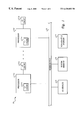
- FIG. 1 depicts a high level block diagram of a multiprocessor data processing system in accordance with the present invention
- FIG. 2 is a block diagram of a load instruction with appended time dependency field (TDF) in accordance with a preferred embodiment of the present invention
- FIG. 3A depicts a detailed block diagram of a load store unit of a processor coupled to an L 2 cache controller and L 2 cache utilized to implement the preferred embodiment of the present invention
- FIG. 3B depicts a block diagram of an intervening L 2 cache in accordance with one embodiment of the present invention.
- FIG. 4 is a block diagram illustrating the generating of a load instruction with appended TDF and subsequent utilization of the TDF within the processor in accordance with one embodiment of the present invention
- FIG. 5 depicts a logic flow chart of the process of loading data with a load instruction containing a TDF in accordance with a preferred embodiment of the present invention
- FIG. 6 depicts an adder component logic for converting a Distance of Dependency (DoD) field to a Cycle of Dependency (CoD) field in accordance with a preferred embodiment of the present invention
- FIG. 7 depicts a flowchart of a multiple TDF load request in accordance with a preferred embodiment of the present invention.
- data processing system 8 includes a number of processors 10 a - 10 n.
- Processors 10 a - 10 n preferably comprises one of the PowerPCTM line of microprocessors available from International Business Machines Corporation; and are superscalar with full out-of-order execution.
- PowerPCTM line of microprocessors available from International Business Machines Corporation; and are superscalar with full out-of-order execution.
- processors 10 a - 10 n preferably comprises one of the PowerPCTM line of microprocessors available from International Business Machines Corporation; and are superscalar with full out-of-order execution.
- processors 10 a - 10 n preferably comprises one of the PowerPCTM line of microprocessors available from International Business Machines Corporation; and are superscalar with full out-of-order execution.
- processors 10 a - 10 n preferably comprises one of the PowerPCTM line of microprocessors available from International Business Machines Corporation; and are superscalar with full out-of-order execution
- each of processors 10 a - 10 n also include an associated on-board level one (L 1 ) data caches 12 a - 12 n, which temporarily holds data that is likely to be accessed by the associated processor.
- L 1 on-board level one
- data processing system 8 may also include one or more additional lower levels of cache, such as level two (L 2 ) caches 15 a - 15 n.
- L 2 caches 15 a - 15 n are depicted as off-chip although it is conceivable that they may be on-chip with L 1 caches 12 a - 12 n.
- the L 2 caches 15 a - 15 n could be traditional inline or lookaside w.r.t. the interconnect, as well as inclusive or non-inclusive of their respective L 1 caches 12 a - 12 n.
- L 2 caches 15 a - 15 n can typically store a much larger amount of data than L 1 caches 12 a - 12 n, but with a longer access latency.
- L 2 caches 15 a - 15 n may have a storage capacity of 4 M-bytes and an access latency of 20 cycles, while L 1 caches 12 a - 12 n may have a storage capacity of 32 kilobytes with an access latency of 2 cycles.
- data processing system 8 further includes input/output (I/O) devices 20 , system memory 18 , and non-volatile storage 22 , which are each coupled to interconnect 16 .
- I/O devices 20 comprise conventional peripheral devices, such as a display device, keyboard, and graphical pointer, which are interfaced to interconnect 16 via conventional adapters.
- Non-volatile storage 22 stores an operating system and other software, which are loaded into volatile system memory 18 in response to data processing system 8 being powered on.
- data processing system 8 can include many additional components which are not shown in FIG. 1, such as serial and parallel ports for connection to network or attached devices, a memory controller that regulates access to system memory 18 , etc.
- Interconnect (system bus) 16 which can comprise one or more buses or a cross-point switch, serves as a conduit for communication transactions between processors 10 a - 10 n, system memory 18 , I/O devices 20 , and nonvolatile storage 22 .
- a typical communication transaction on interconnect 16 includes a source tag indicating the source of the transaction, a destination tag specifying the intended recipient of the transaction, an address, and data.
- Each device coupled to interconnect 16 preferably snoops all communication transactions on interconnect 16 .
- the execution circuitry of processors 10 a - 10 n each comprises multiple execution units, including two fixed-point units (FXU), two load/store units (LSU), and two floating-point units (FPU). As is well-known to those skilled in the computer art, each of the execution units typically executes one or more instructions of a particular type of instructions during each processor cycle.
- FXU fixed-point units
- LSU load/store units
- FPU floating-point units
- Processor 10 employs both pipelining and fully out-of-order execution of instructions to further improve the performance of its superscalar micro-architecture. Accordingly, instructions can be executed by FXU, LSU, and FPU in any order as long as data dependencies are observed.
- LSU typically executes load and store instructions which either load data from L 1 cache or memory (i.e., either L 2 data cache 15 a . . . 15 n or main memory) into selected GPRs, GPR rename buffers, FPRs or FPR rename buffers, etc., or which store data from a selected one of GPRs, GPR rename buffers, FPRs, or FPR rename buffers, etc., to memory.
- LSU typically executes load and store instructions which either load data from L 1 cache or memory (i.e., either L 2 data cache 15 a . . . 15 n or main memory) into selected GPRs, GPR rename buffers, FPRs or FPR rename buffers, etc., or which store data from a selected one of GPRs, GPR rename buffers, FPRs, or FPR rename buffers, etc., to memory.
- the present invention extends the functionality of the LSU during loading of data to allow just
- FIG. 1 depicts only two levels of cache
- the memory hierarchy of data processing system could be expanded to include additional levels (L 3 , L 4 , etc.) of serially-connected caches.
- L 3 , L 4 , etc. additional levels
- FIG. 3A A simple L 1 internal and L 2 external cache topography is utilized in the illustrations for simplicity.
- the preferred embodiment of the present invention appends a time dependency field (TDF) to load instructions.
- TDF is a set of bits which is populated with information which establish on which cycle to load data requested by the load instruction, (i.e., when to send the load request to L 1 or L 2 data cache to effectuate delivery of data at a desired time.) In the preferred embodiment, this is referred to as “just-in-time” delivery of data.
- distance refers to the time period (number of cycles) which exists between the processor issuing a load instruction and when the corresponding load data is actually required by a dependent instruction (i.e., its downstream dependency).
- the processor launches load instructions and sends the time dependency information with the instruction regarding when the load data is needed by the downstream dependency (for example, at 50th cycle).
- this bit field acts as a hint only and depends on the availability of system resources, and other factors.
- the TDF may be included within the instruction set architecture (ISA), or appended during compilation, or dynamically created by hardware during instruction processing.
- TDFs appended to the load instructions as will be discussed below.
- Those skilled in the art understand that any number of TDF fields with differing functionalities may be utilized within the scope of the invention, and that the number of fields actually presented herein are done so for illustrative purposes only.
- the configuration of these TDF fields with respect to a regular load instruction is illustrated in FIG. 2 .
- FIG. 2 depicts a load instruction 200 consisting of information bits such as register location 202 (i.e., where to load the data), and load data requests 204 identifying which data to load. Also, depicted are first TDF 206 A, second TDF 206 B, and third TDF 206 C (collectively referred to hereinafter as TDF 206 unless specifically named or excluded) appended according to the preferred embodiment of the invention. For simplification, discussions of the invention will focus on the first TDF 206 A which is utilized as the DoD and CoD field in the preferred embodiment.
- TDF 206 B utilized as Alternate Preferred Time (APT) and third TDF 206 C utilized as a range of dependency (RoD) will be discussed in detail in the section titled “Multiple TDF Method” below.
- TDF 206 holds the time to load information. This information is utilized to order the load instruction in a time-ordered queue of a data cache controller. The load instruction 200 is then sent to the data cache at a particular time to allow the data to be loaded at the time specified in TDF 206 .
- the TDF field is not present in traditional instruction set architectures (ISA). The dotted lines in FIG. 2 indicates that TDF 206 may or may not be present depending on the ISA of the processor.
- TDF 206 This new ISA includes an Architected TDF (ATDF) which is created by the compiler. Another embodiment utilizes currently available bits in ISA which are redefined to be utilized as the ATDF.
- ATDFs contain general dependency information provided during compilation of the instructions. ATDF (TDF 206 ) are later provided program specific dependency information and converted to an Internal TDF (ITDF) via one of two methods discussed with reference to FIG. 4 .
- Internal TDF (ITDF) (or DoD field) is dynamically created during instruction processing. In multiple TDF embodiments equivalent number of ITDFs are created and include DoD field, Alternate Preferred Time (APT) and range of dependency (RoD) field.
- the ITDF may contain either Distance of Dependency (DoD) or Cycle of Dependency (CoD) information.
- DoD refers to a relative time (number of cycles) between the load request and the load data (for example, in 15 cycles).
- CoD refers to an absolute time based on a Dependency Synchronized Timer (DST) (for example, at cycle 252 ).
- DST is basically a timer within the processor which is synchronized with the DST of the other system components which utilize just-in-time data delivery techniques. For illustrative purposes, it is assumed that a DST runs for 512 cycles (9 bit clock) each period.
- a load instruction with DoD of 100 cycles issue the load request in time for the data to arrive on/immediately after 100 cycles, irrespective of the DST.
- the preferred embodiment of the invention allows for the storage of an “absolute” time in the CoD field corresponding to the DST time the data is actually provided to the execution units.
- the CoD corresponds to DST time the data is actually requested from the L 2 cache.
- the desired absolute time may or may not be available and an “imprecise” time (within a range of cycles from the exact time, will be assigned to the load instruction as will become clear with the description of FIG. 4 and FIG. 7 .
- the utilization of DoD and CoD with load instructions leads to “just-in-time” data delivery.
- the time required for data to travel from the data cache to the requesting process is utilized as an offset to the DoD time and subsequent CoD time (also the RD and SD time).
- This offset allows the load instruction to be issued to the data cache at a time which results in the data arriving at the execution unit at the desired time.
- the offset may be utilized within the calculation of original DoD value or utilized by the time-ordered queue to offset each value during a snoop.
- the time ordered queue may be designed with a delay equal to the offset.
- the preferred embodiment of invention stores “relative” times in the DoD field. Relative time is based on an analysis of all the load instructions and their respective dependent instructions.
- the instructions are received by L 1 cache during program execution either simultaneously or in program order.
- the L 1 cache reschedules them for execution based on their respective DoD fields, thus optimizing the L 1 cache resources.
- one of two dynamic hardware implementations is utilized for appending the priority field.
- the first preferred implementation appends the DoD functionality during the “processing” of instructions in an instruction processor located within the processor of the data processing system.
- the second embodiment is based on an re-configured or newly designed ISA which supports having a TDF appended to regular load instructions as described above.
- the actual DoD information is placed in the DoD field (the new ITDF) by a dependency component/logic within (or external to) the instruction processor.
- FIG. 4 there is depicted a logical view of a dynamic hardware implementation of appending (if necessary) and/or setting the TDF and subsequent utilization of the value in that field to order load instructions from L 1 cache.
- An architected instruction stream 401 (such as, X 86 , PowerPC, etc.) comprising of load instructions of FIG. 2 and other instruction types is sent through an instruction processor 403 where the instructions are processed and converted into hardware specific instructions.
- Instruction processor 403 typically reformats, cracks, combines and reschedules the architected instructions based on the processor design.
- Those skilled in the art are familiar with an instruction processor which takes as input numerous architected instructions and produces an output stream of micro-instructions which are specific to the underlying hardware.
- micro-ops For example, 3.32 bit architected instructions may yield five 19 bit micro-instructions (micro-ops). These unique micro-instructions include load micro-instructions (micro-ops) 415 and other types of micro-instructions (now shown).
- the present invention is concerned only with the novel methods of utilizing an instruction processor to determine a DoD and placing that DoD information in a DoD field which may be either architected by the ISA or created within the instruction processor 403 . Creating hardware specific micro-ops is known in the art.
- micro-ops are separated into load micro-ops 415 and other types of micro-ops.
- the other types of micro-ops are sent to their respective execution units including FPU 407 A and FXU 407 B.
- Load micro-ops 415 with their appended DoD field are sent to LSU 417 .
- the appended load instructions which were originally in program execution order are given a DoD field 413 and other fields 414 utilized during processing. Those skilled in the art are familiar with these other fields 414 and processes by which these other fields 414 are appended.
- the value within DoD field 413 is utilized within LSU 417 to determine “when” to load requested data for each load micro-op 415 .
- Load micro-ops 415 are then sent to LSU 417 where they are scheduled within the relative time-ordered queue (RTOQ) 419 of L 1 cache controller (not shown).
- RTOQ relative time-ordered queue
- the L 1 cache controller determines if the data is available in L 1 cache 420 (i.e. a hit). If the data is available, then the load request is sent to RTOQ 419 which holds the request until the time distance specified (i.e. # of cycles) in DoD field 413 .
- the DoD functionality assumes a non-blocking fixed-delay path from the instruction processor 403 to LSU 417 to respective dependent load instruction (i.e., a known and invariant number of cycles for transmission of the load micro-op 415 from the instruction processor 403 to LSU 417 ). This guarantees the correct reference cycles for DoD.
- an acknowledgement (ACK) signal 422 is sent to the instruction processor which utilizes this information during future ordering (or DoD evaluation) of instructions.
- ACK acknowledgement
- LSU 417 In the event that a miss occurs, LSU 417 then the request for the load data is sent to L 2 cache (not shown).
- This invention implements a series of processes to convert DoD field 413 to a CoD field 425 for utilization by external components such as the L 2 cache and memory. This conversion process is necessary to implement a dependency mechanism at the general system level. The time of propagation of the load request on the system bus as it snoops the external components is not readily ascertainable. It is dependent on system loading, availability of the system bus, etc. These various factors makes it impossible to determine a “relative” time for the load request to be sent to the external component to retrieve the data.
- DST 424 is utilized to synchronize the system components. DST 424 then becomes a reliable reference by which the load request may be dispatched at the correct cycle within the external components.
- the DST time for loading the requested data is represented as a CoD.
- DoD to CoD conversion generation logic 421 is utilized with an input from DST 424 to create a load instruction 423 with appended CoD field 425 as described below.
- the processing of DoD to CoD generation logic 421 requires DST 424 and a non-conventional adder (described with reference to FIG. 5 below) which performs a “X” bit to “X bit+even/odd bit” addition.
- the process may be completed with a conventional adder which for example, takes a 40 bit clock and adds it to a 9 bit DoD field to create a very large 40 bit cycle output.
- This approach requires significant amounts of hardware to implement. Additionally, with this approach, the clock would not be able to handle carry overs and would require suspending the setting of CoD fields for clock cycles close to the end of the period, thus requiring even more logic and hardware to implement.
- FIG. 6 illustrates the adder 601 comprised of adder logic 603 with a first input 605 being the DoD value and a second input 607 being the (9 bit) DST value.
- An additional logic structure (MUX) 609 has as inputs the DST current status 612 (i.e. even or odd) and the carry over value 610 of the adder logic 603 .
- MUX 609 determines whether the time is in an even or odd cycle and stores the answer in even/odd bit 611 of CoD field 613 .
- MUX 609 changes the value of the DST current status 612 .
- CoD field 613 always consist of one additional bit than DoD field. Only the CoD field is shown in this embodiment, however it is understood that this field is appended to a load instruction.
- a DST goes through 512 cycles each period (i.e., a 9 bit clock) and that the maximum CoD for any load instruction is 500 cycles (i.e., also a 9 bit CoD field).
- a load instruction with a DoD value of 300 cycles is received as an input to the adder along with a DST time of 280, then the load data is delivered on cycle 68 of the next DST period.
- the DST time 68 is stored within the 9 bits of CoD.
- this absolute time refers to the next time period, otherwise the dynamic time ordering queue (discussed in FIG. 3 below) becomes confused about where in the queue to place the load instruction.
- the DST is assumed to be alternating between even and odd time periods.
- an even period is represented by a value of 1 and an odd period is represented by a value of 0.
- the adder appends the odd/even bit with its respective value, determined based on whether or not there is a carry over during the known (i.e. even or odd) DST period.
- the DST is always assumed to be even (or odd) for the present cycle and all load instructions for that cycle are given the respective bit, say 0.
- all load instruction still left are assumed to be on the current cycle and their even/odd bit changed to 0.
- the newly added instructions which have a carry over are stored with a 1 even/odd bit and those without a carry over are given a 0 even/odd bit.
- the embodiments presented herein assume that the DoD field holds a value which is less than the DST period; however, those skilled in the art will understand that the various functionalities of the invention may be implemented with DoD values larger than the DST cycle. In such a case, additional logic must be included to allow for the DoD and CoD value to be derived at some distant DST period.
- the nonarchitected micro-ops include only 19 bits.
- the TDF field is made up of 9 bits, then the resulting DoD load micro-ops are 28 bits and the corresponding CoD load micro-ops are 29 bits.
- the preferred embodiment is implemented on a data processing system in which the hardware components, the processor, the LSU and L 1 and L 2 cache, and bus connectors, etc. are designed to recognize a 29 (or 28) bit micro-op (i.e. the extra 9 bits of DoD and/or 10 bits of CoD) and execute the load instructions with these additional bits appended.
- FIG. 3A depicts multiprocessor access to a lower level data (L 2 ) cache.
- Processor 301 and Processor 303 both access a single L 2 cache 317 .
- Both processors 301 and 303 contain at least one load unit (L 1 ) 307 and are connected to L 2 cache 321 via a series of outgoing interconnects (buses) which include cast out/push address bus 308 and load address bus 310 , and a series of incoming interconnects which include L 1 invalidates bus 314 and acknowledgement bus 306 .
- Interconnects for load address 310 contain the load instruction being sent to L 2 cache.
- Load address 310 has an appended cycle of dependency (CoD) field which will be discussed in detail below.
- Return bus 314 also connects L 2 cache 317 to processors 301 and 303 .
- Data buses collectively are utilized for transmitting request for data and data to and from L 2 cache 317 .
- L 2 cache controller 321 contains a directory (not shown) and a dynamic “Time-Ordered Queue” (DTOQ) 305 which orders load and other requests for data from L 2 cache 317 .
- L 2 cache controller 321 also contains various logic structures 309 , 322 and 324 utilized during fetch and receive stages of data requests. Data requests from LSU (L 1 ) 307 are sent as load address 310 to L 2 cache controller 321 .
- L 2 cache controller checks its directory structure to determine if the result of the request is a “hit” or “miss” If it is a hit (i.e. data is present in L 2 cache), then load address 310 is sent to DTOQ 305 to reserve a queue position for delivery of the load data.
- DTOQ 305 orders load address 310 according to its CoD and transmits load address 310 at the precise time requested per its CoD to L 2 cache 317 .
- L 2 cache 317 is gated by a MUX 309 which accepts load address 310 and other simultaneous requests to L 2 cache 317 .
- an acknowledgement (ACK) 306 is transmitted back to the processors 301 and 303 .
- FIG. 3A also depicts system bus (SB) 320 which provides an interconnect between L 2 cache controller 321 and other system components (not shown).
- System bus (SB) 320 has outgoing interconnects 311 including SB address in bus 311 A and SB data in bus 311 B which snoops L 2 cache 317 via L 2 cache controller 321 .
- SB 320 also has incoming interconnects, SB address out bus 313 A and SB data out bus 313 B. Requests for data from L 2 cache 317 are sent to L 2 cache controller 321 via SB address in bus 311 A.
- SB address in bus 311 A also contains a CoD field utilized for ordering its request in dynamic time ordering queue 305 .
- L 2 cache 317 receives load requests 312 and L 2 write requests 316 as inputs. Once a load request 312 is received at L 2 cache 317 , corresponding data is immediately located via address information as is known in the art,and outputted via L 2 read data 318 . L 2 read data 318 is passed through a first logic structure 322 which determines where to deliver the data. Then L 2 read data 318 passes through MUX 324 shown with other inputs. Data requested by L 1 is sent to processors 301 and 303 via return buses 314 . Data requested by external components connected to system bus 320 are sent to external components via SB data out 313 B.
- L 2 cache 317 transmits an ACK signal 306 back to processors 301 and 303 .
- An ACK signal 306 is sent only when load request provides a hit and can be scheduled for the requested cycle. If a hit occurs but there is a conflict with the desired time requested (for example, another load request has already been allotted the time slot), no ACK is sent.
- ACK signal 306 may be a packet, a 1 bit pulse, or any other means utilizing minimal system resources by which L 1 cache is made aware of the availability of the requested time slot for delivery of the data (i.e., the data will be delivered at the cycle specified in the CoD field.).
- ACK signal 306 allows the arbiters and other resources within the processor to more opportunistically prepare for delivery of load data.
- ACK signal as utilized herein provides level information to allow the scheduler or processor to re-optimize based on the availability of lower level resources.
- ACK signal 306 once received, indicates to the processor that it may reserve its pipeline and other resources to that data at the time specified within its CoD field.
- processors 301 and 303 have to predict possible return path and reserve bubbles in pipeline for when it expects the data. This may involve an associative compare process with other data and instructions to determine where data belongs. An incorrect prediction results in bubbles in the pipeline and less efficient processing.
- FIG. 3B depicts an intervening cache 327 with similar configuration as the cache of FIG. 3 A.
- data requested may be in another location, either in memory or another parallel L 2 cache (intervening cache) 327 coupled to another processor.
- the load address is sent via SB address out bus 313 A and system bus 320 to other caches.
- SB address out 313 A contains the load request which includes the appended CoD field.
- This request is sent via system bus to intervening cache 327 which snoops the request and represents the input of SB address in bus 311 C of this structure.
- FIG. 5 there is illustrated a logical flowchart of the process of loading data utilizing a load instruction with appended DoD field.
- the process begins at step 501 .
- a load request is sent to L 1 cache controller with an appended DoD field (step 503 ).
- the L 1 cache controller searches its directory to determine if a hit (step 505 ). If a hit, then the L 1 cache controller checks its RTOQ to see if the requested cycle is available (step 507 ). If it is not available, then the load request is placed at the closest available location within the RTOQ (step 508 ) and the load data is sent on a different cycle (step 528 ). The process then ends (step 529 ).
- step 509 If, the cycle is available, the load request is placed in the queue at that location (step 509 ). An acknowledgement signal is sent to the instruction processor (step 511 ). The data is loaded at the requested pipeline cycle (step 513 ), then the process ends (step 529 ).
- step 505 When there is no hit (i.e. a miss occurs), the DoD is converted to a CoD (step 515 ) as described above.
- the load request is sent to the L 2 cache controller with the appended CoD (step 517 ).
- L 2 cache controller searches its directory to determine if a hit (step 519 ). If a hit, then the L 2 cache controller checks its DTOQ to see if the DST cycle in the DTOQ is available (step 537 ). If it is not available, then the load request is placed at the closest available location within the DTOQ (step 538 ) and the load data is sent on a different cycle (step 528 ). The process then ends (step 529 ).
- the load request is placed in the DTOQ at that location (step 539 ).
- An acknowledgement signal is sent to the processor (step 541 ).
- the data is loaded on the requested DST cycle (step 543 ), then the process ends (step 529 ).
- the load request is sent to the external system components via the system bus (step 521 ).
- the load request searches the directory structures of these external component to determine if a hit (step 523 ). If a hit, and the system component has a time order queue, the system determines if the cycle requested in the time-ordered queue is available (step 537 ).
- the load request is placed in the queue (step 539 ) and the data loaded on the requested DST cycle (step 543 ). Then the process ends (step 529 ). If it is not available, however, the load request is placed at the closest available location (step 538 ) and the data loaded on that cycle (step 528 ). Then the process ends (Step 529 ). The process also ends (step 529 ) when no hit occurs at the external system components.
- FIG. 5 illustrates numerous steps in a sequential fashion for the sake of simplicity, those skilled in the art will appreciate that many of the operations to which the steps pertain may actually be performed in parallel or in a different order.
- the second TDF field is referred to as Alternate Preferred Time (APT) and the third TDF field the range of dependency (RoD).
- the first TDF DoD or CoD
- This APT may then be utilized to select a clock cycle.
- APT may be a neighboring cycle (i.e., 1 cycle away) or many cycles away from the desired time dependency.
- the APT is the same cycle on the next natural loop of the processor pipeline.
- the utilization of multiple TDF fields may also include a third TDF field which provides a range of dependency (RoD).
- RoD refers to a number of cycles before or after the desired cycle (for example, a desired cycle of cycle 50 , with a range of 5 cycles allows the data to be loaded anytime between cycle 45 and cycle 55 ).
- the RoD is equally spread around CoD or DoD, however, it is contemplated that the range may be skewed.
- the invention may allow for a skewed range. In the above example, for instance, data may be loaded anytime between cycle 48 and 57 , or 43 and 52 when the range is 10.
- Those skilled in the art understand the concept of a skewed range to increase processor efficiency.
- the original APT (and RoD) values are also adjusted to reflect corresponding cycles based on the DST time. Skewing the range may be required to enable greater efficiency in providing data to a process which may prefer the data earlier or later when the desired time is not available.
- the RoD, when utilized as a raw number (range of 10) around the desired time is not adjusted during DoD to CoD conversion.
- FIG. 7 depicts the process of ordering load instructions of FIG. 5 during multiple TDF implementation.
- the process begins (step 701 ) when the time ordered queue is checked for the availability of the requested cycle (i.e., the DoD or CoD) (step 703 ). If the cycle is available, the load instruction is placed in time ordered queue at the requested cycle (DoD or CoD) (step 705 ). If, however, the cycle is unavailable the process then checks for the availability of the Alternate Preferred Time (APT) cycle (step 707 ). If the APT cycle is available, the load instruction is placed in the time ordered queue at that cycle (step 709 ).
- APT Alternate Preferred Time
- step 715 If, the APT cycle is unavailable, another check is made for the availability of a cycle within a range of dependencies (RoD) (step 715 ). If available, the load instruction is placed in the time ordered queue at a cycle time ordered queue within the range of dependency (RoD) (step 717 ). If, however, no cycle is available within the RoD, the load instruction is placed at an open/cycle within time ordered queue (step 711 ). Once the load instruction is placed in the time ordered queue, the process ends (step 713 ). Although not shown, those killed in the art appreciated that many other process steps are possible in attempting to place the load instruction within the time ordered queue. Once all pre-defined steps have been the instruction is placed at a random location which is available.
- RoD range of dependencies
- the process of sending an ACK is extended to the multiple TDF embodiment.
- a different ACK is sent for each TDF.
- Each ACK is coded to allow the system resources to decipher which TDF is actually being acknowledged.
- the corresponding ACK is sent and the system resources reserve pipeline based on the TDF.
- the RoD allows the system resources to determine if an available pipeline bubble exists within that range and to allocate that bubble to the load data.
Abstract
Description
Claims (20)
Priority Applications (1)
| Application Number | Priority Date | Filing Date | Title |
|---|---|---|---|
| US09/344,023 US6430683B1 (en) | 1999-06-25 | 1999-06-25 | Processor and method for just-in-time delivery of load data via time dependency field |
Applications Claiming Priority (1)
| Application Number | Priority Date | Filing Date | Title |
|---|---|---|---|
| US09/344,023 US6430683B1 (en) | 1999-06-25 | 1999-06-25 | Processor and method for just-in-time delivery of load data via time dependency field |
Publications (1)
| Publication Number | Publication Date |
|---|---|
| US6430683B1 true US6430683B1 (en) | 2002-08-06 |
Family
ID=23348711
Family Applications (1)
| Application Number | Title | Priority Date | Filing Date |
|---|---|---|---|
| US09/344,023 Expired - Fee Related US6430683B1 (en) | 1999-06-25 | 1999-06-25 | Processor and method for just-in-time delivery of load data via time dependency field |
Country Status (1)
| Country | Link |
|---|---|
| US (1) | US6430683B1 (en) |
Cited By (8)
| Publication number | Priority date | Publication date | Assignee | Title |
|---|---|---|---|---|
| US20020099927A1 (en) * | 2001-01-22 | 2002-07-25 | Steely Simon C. | System and method for determining operand access to data |
| US6950926B1 (en) * | 2001-03-02 | 2005-09-27 | Advanced Micro Devices, Inc. | Use of a neutral instruction as a dependency indicator for a set of instructions |
| US20060149933A1 (en) * | 2004-12-17 | 2006-07-06 | International Business Machines Corp. | Branch lookahead prefetch for microprocessors |
| US20060149934A1 (en) * | 2004-12-17 | 2006-07-06 | Eickemever Richard J | Using a modified value GPR to enhance lookahead prefetch |
| US20060149935A1 (en) * | 2004-12-17 | 2006-07-06 | International Business Machines Corporation | Load lookahead prefetch for microprocessors |
| US20070150687A1 (en) * | 2005-12-23 | 2007-06-28 | Intel Corporation | Memory system with both single and consolidated commands |
| US7430686B1 (en) | 2002-10-09 | 2008-09-30 | Xpoint Technologies, Inc. | Data processing recovery system and method spanning multiple operating system |
| US10185568B2 (en) * | 2016-04-22 | 2019-01-22 | Microsoft Technology Licensing, Llc | Annotation logic for dynamic instruction lookahead distance determination |
Citations (20)
| Publication number | Priority date | Publication date | Assignee | Title |
|---|---|---|---|---|
| US5214765A (en) | 1989-08-31 | 1993-05-25 | Sun Microsystems, Inc. | Method and apparatus for executing floating point instructions utilizing complimentary floating point pipeline and multi-level caches |
| US5278985A (en) * | 1990-10-31 | 1994-01-11 | Hewlett-Packard Company | Software method for implementing dismissible instructions on a computer |
| US5307477A (en) | 1989-12-01 | 1994-04-26 | Mips Computer Systems, Inc. | Two-level cache memory system |
| US5404484A (en) * | 1992-09-16 | 1995-04-04 | Hewlett-Packard Company | Cache system for reducing memory latency times |
| US5694574A (en) | 1994-01-04 | 1997-12-02 | Intel Corporation | Method and apparatus for performing load operations in a computer system |
| US5717882A (en) | 1994-01-04 | 1998-02-10 | Intel Corporation | Method and apparatus for dispatching and executing a load operation to memory |
| US5737565A (en) | 1995-08-24 | 1998-04-07 | International Business Machines Corporation | System and method for diallocating stream from a stream buffer |
| US5758051A (en) | 1996-07-30 | 1998-05-26 | International Business Machines Corporation | Method and apparatus for reordering memory operations in a processor |
| US5761515A (en) | 1996-03-14 | 1998-06-02 | International Business Machines Corporation | Branch on cache hit/miss for compiler-assisted miss delay tolerance |
| US5809275A (en) | 1996-03-01 | 1998-09-15 | Hewlett-Packard Company | Store-to-load hazard resolution system and method for a processor that executes instructions out of order |
| US5895495A (en) | 1997-03-13 | 1999-04-20 | International Business Machines Corporation | Demand-based larx-reserve protocol for SMP system buses |
| US5964867A (en) | 1997-11-26 | 1999-10-12 | Digital Equipment Corporation | Method for inserting memory prefetch operations based on measured latencies in a program optimizer |
| US5987594A (en) | 1997-06-25 | 1999-11-16 | Sun Microsystems, Inc. | Apparatus for executing coded dependent instructions having variable latencies |
| US5999727A (en) | 1997-06-25 | 1999-12-07 | Sun Microsystems, Inc. | Method for restraining over-eager load boosting using a dependency color indicator stored in cache with both the load and store instructions |
| US6006326A (en) | 1997-06-25 | 1999-12-21 | Sun Microsystems, Inc. | Apparatus for restraining over-eager load boosting in an out-of-order machine using a memory disambiguation buffer for determining dependencies |
| US6052775A (en) | 1997-06-25 | 2000-04-18 | Sun Microsystems, Inc. | Method for non-intrusive cache fills and handling of load misses |
| US6058472A (en) | 1997-06-25 | 2000-05-02 | Sun Microsystems, Inc. | Apparatus for maintaining program correctness while allowing loads to be boosted past stores in an out-of-order machine |
| US6065101A (en) | 1997-06-12 | 2000-05-16 | International Business Machines Corporation | Pipelined snooping of multiple L1 cache lines |
| US6092180A (en) | 1997-11-26 | 2000-07-18 | Digital Equipment Corporation | Method for measuring latencies by randomly selected sampling of the instructions while the instruction are executed |
| US6145059A (en) | 1998-02-17 | 2000-11-07 | International Business Machines Corporation | Cache coherency protocols with posted operations and tagged coherency states |
-
1999
- 1999-06-25 US US09/344,023 patent/US6430683B1/en not_active Expired - Fee Related
Patent Citations (20)
| Publication number | Priority date | Publication date | Assignee | Title |
|---|---|---|---|---|
| US5214765A (en) | 1989-08-31 | 1993-05-25 | Sun Microsystems, Inc. | Method and apparatus for executing floating point instructions utilizing complimentary floating point pipeline and multi-level caches |
| US5307477A (en) | 1989-12-01 | 1994-04-26 | Mips Computer Systems, Inc. | Two-level cache memory system |
| US5278985A (en) * | 1990-10-31 | 1994-01-11 | Hewlett-Packard Company | Software method for implementing dismissible instructions on a computer |
| US5404484A (en) * | 1992-09-16 | 1995-04-04 | Hewlett-Packard Company | Cache system for reducing memory latency times |
| US5694574A (en) | 1994-01-04 | 1997-12-02 | Intel Corporation | Method and apparatus for performing load operations in a computer system |
| US5717882A (en) | 1994-01-04 | 1998-02-10 | Intel Corporation | Method and apparatus for dispatching and executing a load operation to memory |
| US5737565A (en) | 1995-08-24 | 1998-04-07 | International Business Machines Corporation | System and method for diallocating stream from a stream buffer |
| US5809275A (en) | 1996-03-01 | 1998-09-15 | Hewlett-Packard Company | Store-to-load hazard resolution system and method for a processor that executes instructions out of order |
| US5761515A (en) | 1996-03-14 | 1998-06-02 | International Business Machines Corporation | Branch on cache hit/miss for compiler-assisted miss delay tolerance |
| US5758051A (en) | 1996-07-30 | 1998-05-26 | International Business Machines Corporation | Method and apparatus for reordering memory operations in a processor |
| US5895495A (en) | 1997-03-13 | 1999-04-20 | International Business Machines Corporation | Demand-based larx-reserve protocol for SMP system buses |
| US6065101A (en) | 1997-06-12 | 2000-05-16 | International Business Machines Corporation | Pipelined snooping of multiple L1 cache lines |
| US5987594A (en) | 1997-06-25 | 1999-11-16 | Sun Microsystems, Inc. | Apparatus for executing coded dependent instructions having variable latencies |
| US5999727A (en) | 1997-06-25 | 1999-12-07 | Sun Microsystems, Inc. | Method for restraining over-eager load boosting using a dependency color indicator stored in cache with both the load and store instructions |
| US6006326A (en) | 1997-06-25 | 1999-12-21 | Sun Microsystems, Inc. | Apparatus for restraining over-eager load boosting in an out-of-order machine using a memory disambiguation buffer for determining dependencies |
| US6052775A (en) | 1997-06-25 | 2000-04-18 | Sun Microsystems, Inc. | Method for non-intrusive cache fills and handling of load misses |
| US6058472A (en) | 1997-06-25 | 2000-05-02 | Sun Microsystems, Inc. | Apparatus for maintaining program correctness while allowing loads to be boosted past stores in an out-of-order machine |
| US5964867A (en) | 1997-11-26 | 1999-10-12 | Digital Equipment Corporation | Method for inserting memory prefetch operations based on measured latencies in a program optimizer |
| US6092180A (en) | 1997-11-26 | 2000-07-18 | Digital Equipment Corporation | Method for measuring latencies by randomly selected sampling of the instructions while the instruction are executed |
| US6145059A (en) | 1998-02-17 | 2000-11-07 | International Business Machines Corporation | Cache coherency protocols with posted operations and tagged coherency states |
Non-Patent Citations (5)
| Title |
|---|
| U.S. application No. 09/338,946, Ravi K. Arimilli et al., filed Jun. 25, 1999. |
| U.S. application No. 09/344,057, Ravi K. Arimilli et al., filed Jun. 25, 1999. |
| U.S. application No. 09/344,058, Ravi K. Arimilli et al., filed Jun. 25, 1999. |
| U.S. application No. 09/344,060, Ravi K. Arimilli et al., filed Jun. 25, 1999. |
| U.S. application No. 09/344,061, Ravi K. Arimilli et al., filed Jun. 25, 1999. |
Cited By (21)
| Publication number | Priority date | Publication date | Assignee | Title |
|---|---|---|---|---|
| US20020099927A1 (en) * | 2001-01-22 | 2002-07-25 | Steely Simon C. | System and method for determining operand access to data |
| US6769057B2 (en) * | 2001-01-22 | 2004-07-27 | Hewlett-Packard Development Company, L.P. | System and method for determining operand access to data |
| US6950926B1 (en) * | 2001-03-02 | 2005-09-27 | Advanced Micro Devices, Inc. | Use of a neutral instruction as a dependency indicator for a set of instructions |
| US7430686B1 (en) | 2002-10-09 | 2008-09-30 | Xpoint Technologies, Inc. | Data processing recovery system and method spanning multiple operating system |
| US7421567B2 (en) | 2004-12-17 | 2008-09-02 | International Business Machines Corporation | Using a modified value GPR to enhance lookahead prefetch |
| US7444498B2 (en) * | 2004-12-17 | 2008-10-28 | International Business Machines Corporation | Load lookahead prefetch for microprocessors |
| US7877580B2 (en) | 2004-12-17 | 2011-01-25 | International Business Machines Corporation | Branch lookahead prefetch for microprocessors |
| US7620799B2 (en) | 2004-12-17 | 2009-11-17 | International Business Machines Corporation | Using a modified value GPR to enhance lookahead prefetch |
| US20080077776A1 (en) * | 2004-12-17 | 2008-03-27 | Eickemeyer Richard J | Load Lookahead Prefetch for Microprocessors |
| US20080091928A1 (en) * | 2004-12-17 | 2008-04-17 | Eickemeyer Richard J | Branch lookahead prefetch for microprocessors |
| US20060149934A1 (en) * | 2004-12-17 | 2006-07-06 | Eickemever Richard J | Using a modified value GPR to enhance lookahead prefetch |
| US20060149933A1 (en) * | 2004-12-17 | 2006-07-06 | International Business Machines Corp. | Branch lookahead prefetch for microprocessors |
| US20080250230A1 (en) * | 2004-12-17 | 2008-10-09 | International Business Machines Corporation | Using a Modified Value GPR to Enhance Lookahead Prefetch |
| US20060149935A1 (en) * | 2004-12-17 | 2006-07-06 | International Business Machines Corporation | Load lookahead prefetch for microprocessors |
| US7552318B2 (en) | 2004-12-17 | 2009-06-23 | International Business Machines Corporation | Branch lookahead prefetch for microprocessors |
| US7594096B2 (en) | 2004-12-17 | 2009-09-22 | International Business Machines Corporation | Load lookahead prefetch for microprocessors |
| US20070150688A1 (en) * | 2005-12-23 | 2007-06-28 | Intel Corporation | Chips providing single and consolidated commands |
| US7673111B2 (en) | 2005-12-23 | 2010-03-02 | Intel Corporation | Memory system with both single and consolidated commands |
| US7752411B2 (en) * | 2005-12-23 | 2010-07-06 | Intel Corporation | Chips providing single and consolidated commands |
| US20070150687A1 (en) * | 2005-12-23 | 2007-06-28 | Intel Corporation | Memory system with both single and consolidated commands |
| US10185568B2 (en) * | 2016-04-22 | 2019-01-22 | Microsoft Technology Licensing, Llc | Annotation logic for dynamic instruction lookahead distance determination |
Similar Documents
| Publication | Publication Date | Title |
|---|---|---|
| US6950925B1 (en) | Scheduler for use in a microprocessor that supports data-speculative execution | |
| US7415597B2 (en) | Processor with dependence mechanism to predict whether a load is dependent on older store | |
| US5778434A (en) | System and method for processing multiple requests and out of order returns | |
| US6523109B1 (en) | Store queue multimatch detection | |
| EP1228426B1 (en) | Store buffer which forwards data based on index and optional way match | |
| US7213126B1 (en) | Method and processor including logic for storing traces within a trace cache | |
| US7028166B2 (en) | System and method for linking speculative results of load operations to register values | |
| US6622237B1 (en) | Store to load forward predictor training using delta tag | |
| US7133969B2 (en) | System and method for handling exceptional instructions in a trace cache based processor | |
| CN100495325C (en) | Method and system for on-demand scratch register renaming | |
| US6651161B1 (en) | Store load forward predictor untraining | |
| US6481251B1 (en) | Store queue number assignment and tracking | |
| US20020087849A1 (en) | Full multiprocessor speculation mechanism in a symmetric multiprocessor (smp) System | |
| US6694424B1 (en) | Store load forward predictor training | |
| GB2287111A (en) | Pipelined processing of instructions | |
| US6721877B1 (en) | Branch predictor that selects between predictions based on stored prediction selector and branch predictor index generation | |
| US6427204B1 (en) | Method for just in-time delivery of instructions in a data processing system | |
| US6389529B1 (en) | Method for alternate preferred time delivery of load data | |
| US6425090B1 (en) | Method for just-in-time delivery of load data utilizing alternating time intervals | |
| TWI457827B (en) | Distributed dispatch with concurrent, out-of-order dispatch | |
| US20030126409A1 (en) | Store sets poison propagation | |
| EP1644823A1 (en) | Load store unit with replay mechanism | |
| US6430683B1 (en) | Processor and method for just-in-time delivery of load data via time dependency field | |
| US6704854B1 (en) | Determination of execution resource allocation based on concurrently executable misaligned memory operations | |
| US7043626B1 (en) | Retaining flag value associated with dead result data in freed rename physical register with an indicator to select set-aside register instead for renaming |
Legal Events
| Date | Code | Title | Description |
|---|---|---|---|
| AS | Assignment |
Owner name: INTERNATIONAL BUSINESS MACHINES CORPORATION, NEW Y Free format text: ASSIGNMENT OF ASSIGNORS INTEREST;ASSIGNORS:ARIMILLI, RAVI K.;ARIMILLI, LAKSHMINARAYANAN B.;DODSON, JOHN S.;AND OTHERS;REEL/FRAME:010071/0960 Effective date: 19990618 |
|
| AS | Assignment |
Owner name: INTERNATIONAL BUSINESS MACHINES CORPORATION, NEW Y Free format text: ASSIGNMENT OF ASSIGNORS INTEREST;ASSIGNOR:ARIMILLI, LAKSHMINARAYANA B.;REEL/FRAME:010367/0116 Effective date: 19991007 Owner name: INTERNATIONAL BUSINESS MACHINES CORPORATION, NEW Y Free format text: ASSIGNMENT OF ASSIGNORS INTEREST;ASSIGNOR:LAKSHMINARAYANA B. ARIMILLI;REEL/FRAME:010367/0149 Effective date: 19991007 Owner name: INTERNATIONAL BUSINESS MACHINES CORPORATION, NEW Y Free format text: ASSIGNMENT OF ASSIGNORS INTEREST;ASSIGNOR:ARIMILLI, LADSHMINARAYANA B.;REEL/FRAME:010367/0218 Effective date: 19991007 |
|
| FPAY | Fee payment |
Year of fee payment: 4 |
|
| REMI | Maintenance fee reminder mailed | ||
| LAPS | Lapse for failure to pay maintenance fees | ||
| STCH | Information on status: patent discontinuation |
Free format text: PATENT EXPIRED DUE TO NONPAYMENT OF MAINTENANCE FEES UNDER 37 CFR 1.362 |
|
| FP | Lapsed due to failure to pay maintenance fee |
Effective date: 20100806 |