US6400624B1 - Configure registers and loads to tailor a multi-level cell flash design - Google Patents
Configure registers and loads to tailor a multi-level cell flash design Download PDFInfo
- Publication number
- US6400624B1 US6400624B1 US09/794,479 US79447901A US6400624B1 US 6400624 B1 US6400624 B1 US 6400624B1 US 79447901 A US79447901 A US 79447901A US 6400624 B1 US6400624 B1 US 6400624B1
- Authority
- US
- United States
- Prior art keywords
- values
- configure
- performance
- memory device
- program
- Prior art date
- Legal status (The legal status is an assumption and is not a legal conclusion. Google has not performed a legal analysis and makes no representation as to the accuracy of the status listed.)
- Expired - Lifetime
Links
- 230000015654 memory Effects 0.000 claims abstract description 97
- 238000012360 testing method Methods 0.000 claims abstract description 37
- 238000000034 method Methods 0.000 claims abstract description 17
- 238000003860 storage Methods 0.000 claims description 14
- 230000004044 response Effects 0.000 claims description 10
- 210000004027 cell Anatomy 0.000 description 85
- 238000009826 distribution Methods 0.000 description 14
- 239000002184 metal Substances 0.000 description 8
- 238000010586 diagram Methods 0.000 description 4
- 238000005457 optimization Methods 0.000 description 4
- 230000000630 rising effect Effects 0.000 description 3
- 230000004913 activation Effects 0.000 description 2
- 230000008901 benefit Effects 0.000 description 2
- 230000003993 interaction Effects 0.000 description 2
- 238000004519 manufacturing process Methods 0.000 description 2
- 239000011159 matrix material Substances 0.000 description 2
- 238000012986 modification Methods 0.000 description 2
- 230000004048 modification Effects 0.000 description 2
- 210000000352 storage cell Anatomy 0.000 description 2
- XUIMIQQOPSSXEZ-UHFFFAOYSA-N Silicon Chemical compound [Si] XUIMIQQOPSSXEZ-UHFFFAOYSA-N 0.000 description 1
- 238000012512 characterization method Methods 0.000 description 1
- 238000006243 chemical reaction Methods 0.000 description 1
- 238000013500 data storage Methods 0.000 description 1
- 230000009977 dual effect Effects 0.000 description 1
- 230000000873 masking effect Effects 0.000 description 1
- 238000001465 metallisation Methods 0.000 description 1
- 230000008569 process Effects 0.000 description 1
- 230000002441 reversible effect Effects 0.000 description 1
- 239000004065 semiconductor Substances 0.000 description 1
- 229910052710 silicon Inorganic materials 0.000 description 1
- 239000010703 silicon Substances 0.000 description 1
- 238000004088 simulation Methods 0.000 description 1
- 230000003068 static effect Effects 0.000 description 1
Images


Classifications
-
- G—PHYSICS
- G11—INFORMATION STORAGE
- G11C—STATIC STORES
- G11C29/00—Checking stores for correct operation ; Subsequent repair; Testing stores during standby or offline operation
- G11C29/02—Detection or location of defective auxiliary circuits, e.g. defective refresh counters
- G11C29/028—Detection or location of defective auxiliary circuits, e.g. defective refresh counters with adaption or trimming of parameters
-
- G—PHYSICS
- G11—INFORMATION STORAGE
- G11C—STATIC STORES
- G11C11/00—Digital stores characterised by the use of particular electric or magnetic storage elements; Storage elements therefor
- G11C11/56—Digital stores characterised by the use of particular electric or magnetic storage elements; Storage elements therefor using storage elements with more than two stable states represented by steps, e.g. of voltage, current, phase, frequency
- G11C11/5621—Digital stores characterised by the use of particular electric or magnetic storage elements; Storage elements therefor using storage elements with more than two stable states represented by steps, e.g. of voltage, current, phase, frequency using charge storage in a floating gate
-
- G—PHYSICS
- G11—INFORMATION STORAGE
- G11C—STATIC STORES
- G11C16/00—Erasable programmable read-only memories
- G11C16/02—Erasable programmable read-only memories electrically programmable
- G11C16/04—Erasable programmable read-only memories electrically programmable using variable threshold transistors, e.g. FAMOS
- G11C16/0483—Erasable programmable read-only memories electrically programmable using variable threshold transistors, e.g. FAMOS comprising cells having several storage transistors connected in series
-
- G—PHYSICS
- G11—INFORMATION STORAGE
- G11C—STATIC STORES
- G11C29/00—Checking stores for correct operation ; Subsequent repair; Testing stores during standby or offline operation
- G11C29/04—Detection or location of defective memory elements, e.g. cell constructio details, timing of test signals
- G11C29/50—Marginal testing, e.g. race, voltage or current testing
- G11C29/50004—Marginal testing, e.g. race, voltage or current testing of threshold voltage
-
- G—PHYSICS
- G11—INFORMATION STORAGE
- G11C—STATIC STORES
- G11C16/00—Erasable programmable read-only memories
- G11C16/02—Erasable programmable read-only memories electrically programmable
- G11C16/04—Erasable programmable read-only memories electrically programmable using variable threshold transistors, e.g. FAMOS
Definitions
- the present invention relates generally to memory devices. More particularly, the present invention relates to a descending staircase read technique for a multi-level cell NAND flash memory device.
- Nonvolatile memory provides a key advantage in that it retains stored data after power is removed from the device.
- One example of nonvolatile memory is flash memory.
- manufacture and operation of nonvolatile memory is generally more complex than for volatile memory.
- important design goals include increased storage density and reduced read and write times.
- a conventional memory device includes an array of storage cells or memory cells. Each cell stores a single binary digit or bit of information. For example, in a flash memory, the threshold voltage of a transistor in the memory cell is adjusted according to the data stored. During a read cycle, the threshold voltage is sensed to resolve the state of the data stored. In a conventional binary memory, this data is conventionally described as having a state of logic 0 or logic 1.
- the array of storage cells is surrounded by circuits for reading and writing data and controlling operation of the memory device.
- Multi-level storage refers to the ability of a single memory cell to store or represent more than a single bit of data.
- a multi-level cell may store 2, 4, 8 . . . etc., bits in a single storage location.
- Multi-level storage is achieved by storing charge on a floating gate of a memory cell to establish a threshold voltage Vt level for the cell from among three or more possible threshold voltages. The actual Vt produced will fall within a program distribution with some allowed tolerance still providing reliable operation.
- program pulse count or the number of signal pulses that must be applied to a memory cell to program the cell to a selected level
- program pulse width or the time duration of signal pulses which program the cell
- read verify reference current or the current used as a reference when resolving the stored state of the memory cell
- program inhibit voltage and read pass voltage Such parameters are referred to herein as performance variables, although once established they may not vary but instead remain constant.
- the first technique involves metal options for the integrated circuit. Metal masks may be changed or the silicon connections may be post-processed after most or all of the conventional masking steps to optimize performance variables. These metal option methods are time consuming and are generally not reversible, so that re-optimization later is not possible. There is no test flexibility with these metal options, so that a performance variable may be programmed once at one test condition (operating voltage, temperature, etc.) with no opportunity to adjust the performance variable at another test condition. Many memory devices must be prepared and tested to examine interaction of variables. With a large number of performance variables, it is impossible to investigate a full design matrix.
- a second technique has been used to generate performance variables in flash memory devices involves the use of content addressable memory or CAM cells consisting of a single flash memory cell.
- CAM cells are flexible and may be repeatedly programmed and erased, overcoming the chief limitation of metal options.
- CAM cells introduce a significant die size penalty.
- Each CAM cell must have its own high voltage circuit to generate the necessary program and erase voltages.
- programming and erasing of memory cells requires significant time and increases testing complexity. In conventional designs, all CAM cells are erased together, meaning that the old state must be stored to return to default settings.
- a method for testing a multi-level memory includes storing multi-level data in a plurality of memory cells of the multi-level memory and reading from configure registers initial values of a plurality of performance variables.
- the performance variables set operating parameters of the multi-level memory.
- the method further includes during a first test phase operating the multi-level memory at the initial values of the plurality of performance variables and reading program values of the plurality of performance variables.
- the multi-level memory is operated at the program values of the plurality of performance variables.
- FIG. 1 is a block diagram of a memory device
- FIG. 2 is a simplified block diagram illustrating a read operation in the memory device of FIG. 1;
- FIG. 3 illustrates relative threshold voltage levels for storing data in a multi-level memory cell of the memory device of FIG. 1;
- FIG. 4 illustrates configure registers for storing performance variable data in a multi-level memory cell.
- FIG. 1 shows a block diagram of a memory device 100 .
- the memory device 100 in the illustrated embodiment is a NAND flash memory.
- the memory device 100 may be any other suitable type of volatile memory such as random access memory (RAM) including static or dynamic RAM or nonvolatile memory such as EEPROM.
- RAM random access memory
- EEPROM nonvolatile memory
- the memory device 100 may be an embedded memory circuit within another integrated circuit or device containing other circuitry, such as logic.
- the memory device 100 may be written or programmed with data, read to retrieve the stored data, and erased to clear the memory device on a block-by-block basis.
- the memory device 100 includes a memory cell array 102 , an input/output (I/O) register 104 , one or more Y-decoders 106 , one or more sense amplifier blocks 108 and one or more X-decoders 110 . Further, the memory device 100 includes a command register 112 , a state machine 114 , an address register 116 , a status register 118 and a high voltage circuit 120 . Other embodiments of the memory device 100 may include other components or omit some of those illustrated in FIG. 1 .
- the memory cell array 102 includes a plurality of memory cells arranged in an ordered array of rows and columns. Each memory cell is independently addressable and may be programmed or written with data and read or sensed. In response to a received address, the X-decoder 110 selects one or more rows of the memory cell array 102 for access. Similarly, the Y-decoder 106 selects one or more columns of the memory cell array 102 for access. Sense amplifiers in the sense amplifier block 108 detect the state of the data stored in the accessed memory cell or cells. Data registers of the sense amplifier block 108 store data immediately prior to writing or immediately after reading the accessed memory cell or cells.
- Reading data is done according to standard NAND flash operation.
- a starting address is provided to the I/O register 104 along with the appropriate command.
- the associated memory cells are accessed and a page of data is transferred to the I/O register 104 .
- a page may be any suitable size, such as 264 bytes.
- the 264 bytes in this example includes 256 bytes of storage area and 8 bytes of spare area.
- an initial page read access time such as 6 microseconds
- the memory device 100 under control of the state machine 114 automatically increments the address register to the next address location in response to a received clock signal.
- Erasing operations are performed on a block basis.
- a block may be any suitable size, such as 16 rows by 256 words per row.
- the state machine 114 initiates an embedded erase algorithm to automatically time erase pulse widths and verify proper cell erase margin.
- the memory device 100 signals completion of an operation such as a read, write or erase using a read/busy pin 122 .
- the signal at the ready/busy pin 122 indicates operation status of the memory device 100 . When this signal is high, the memory device 100 is ready to accept commands and data for a next operation. When the signal at the pin 122 is low, an internal operation is in progress.
- the high voltage circuit 120 generates the voltages necessary for proper reading, programming and erasure of the memory device 100 .
- the memory device 100 operates in response to power supply (Vcc and Vccq) and ground (Vss) voltages.
- Typical power supply voltage is 3.0 volts, but other voltages may be used.
- a write protect input pin 124 provides hardware data protection. When a write protect signal is asserted at pin 124 , program and erase operations are inhibited.
- a command latch enable (CLE) pin 126 receives a signal which controls activation of the command register 112 for the receipt of commands. When this signal is high, the command is latched into the command register 112 on the rising edge of the write enable signal received at the write enable pin 128 .
- a signal at an address latch enable (ALE) input 130 controls activation of the address register 116 during a data input operation. When the ALE signal is high, the address information is latched on the rising edge of the write enable signal at pin 128 . When ALE is low, the input data information is latched on the rising edge of the write enable signal.
- the signal at the chip enable input 132 controls the mode, either active or standby, of the memory device 100 .
- the signal at the read enable input 134 controls serial data output and status from the input/output lines.
- the signal at the spare area enable input 136 controls access to a spare storage area on each page. When the spare area signal is high, the spare area is not enabled.
- the memory device 100 stores several internal parameters which affect performance of the memory. Examples of such parameters include: program pulse count, or the number of signal pulses that must be applied to a memory cell to program the cell to a selected level; program pulse width, or the time duration of signal pulses which program the cell; read verify reference current, or the current used as a reference when resolving the stored state of the memory cell; program inhibit voltage and read pass voltage. Such parameters are referred to herein as performance variables. In one embodiment, these parameters are stored in the state machine 114 . In other embodiments, these parameters are stored elsewhere in the memory device and their reading, programming and erasing is under control of one or more control circuits. Further details will be provided below in conjunction with FIG. 4 .
- FIG. 2 is a simplified block diagram illustrating a read operation in the memory device of FIG. 1 .
- FIG. 2 shows two columns including a first column 202 and a second column 204 of the memory cell array 102 .
- Each column 202 , 204 includes a column current source 206 , 208 , respectively, bit line buffer logic 210 , 212 respectively, a cascode transistor 216 , 218 , and a plurality of memory cells.
- the cascode transistors 216 , 218 have respective sources coupled to the bit lines 220 , 222 , respectively, and respective drains coupled to the sense lines 224 , 226 .
- the gates of the cascode transistors 216 , 218 are coupled to a reference potential.
- the cascode transistors 216 , 218 form cascode amplifiers to amplify the current in the bit line due to a selected memory cell for sensing at the sense lines 224 , 226 .
- the memory cells are arranged in an array of rows and columns. In a typical embodiment, there are 16 memory cells per column and 264 memory cells per row. Memory cells are further organized in pages, blocks and sectors. The rows are interconnected by word lines including a word line 214 shown in FIG. 2 .
- each memory cell of the flash memory includes a floating gate for storage of charge.
- the threshold voltage of the memory cell is adjusted.
- the memory cell transistor conducts current.
- other transistors in the column are supplied with a voltage Vpass so that these transistors act as pass transistors, conducting the current sunk in the memory cell to the bit lines 220 , 222 .
- This current is amplified by the cascode transistors 216 , 218 .
- transistor 230 is selected by driving the word line 214 to a read voltage. This same voltage is applied to all memory cells coupled to the word line 214 , such as transistor 232 in column 204 .
- the threshold voltage Vt of the cell is less than the applied read voltage (RD). Therefore, the memory cell 230 will conduct a read current on the order of a few microamps.
- This current in the bit line 220 is amplified by the cascode transistor 216 and the sense line 224 is pulled low to a voltage of approximately Vss.
- the bit line buffer circuitry 210 embodied here as a D latch 240 , will store the state of the sense line 224 and the data may be read from the latch 240 .
- the threshold voltage Vt of the memory cell 232 is greater than the applied read voltage (RD) on the word line 214 .
- the memory cell 232 will conduct substantially no current.
- the bit line buffer circuitry 210 is embodied as a D latch 242 which stores the state of the sense line 226 for subsequent reading.
- FIG. 3 illustrates relative threshold voltage levels for storing data in a multi-level memory cell of the memory device of FIG. 1 .
- the erased data state or E has the most negative programmed threshold voltage in a distribution 302 so that erased memory cells will always conduct when their associated word line is selected or driven to a relatively high voltage level.
- a data state of 0 has the next highest programmed threshold voltage, in a distribution 304 .
- a data state of 1 has the next highest programmed threshold voltage, in a distribution 306 .
- a data state of 2 has the highest programmed threshold voltage, in a distribution 308 .
- Vt Q2 Q1 2 2.0 V 0 0 1 1.0 V 0 1 0 0 V 1 0 E ⁇ 2.0 V 1 1
- FIG. 3 further shows the read levels required to resolve the data stored in a given memory cell.
- a first read level 310 labelled Rd 0 is used to discriminate the stored 0 data from an erased state. That is, a voltage Rd 0 is applied to the word line of the memory cell to be sensed. If the memory cell stores an erased state E, the threshold voltage of the memory cell will be in the distribution 302 and therefore less than the applied voltage Rd 0 . The memory cell will conduct current. On the other hand, if the memory cell stores the data 0 state, the threshold voltage will be in the distribution 304 and therefore greater than the applied voltage Rd 0 . The memory cell will not conduct current or will conduct only leakage current.
- a descending staircase read signal with levels substantially equal to voltage Rd 2 , Rd 1 and Rd 0 is applied to a selected memory cell to distinguish possible stored voltages in a memory cell.
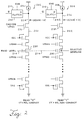
- FIG. 4 illustrates configure registers 400 for storing performance variable data in a multi-level memory cell.
- the configure registers 400 include a first configure register 402 and a second configure register 404 .
- the circuit shown in the drawing is exemplary only.
- An integrated circuit such as a memory may include a large number of configure registers to establish performance variables for operating and testing the integrated circuit.
- Each configure register 402 , 404 includes a first data input 406 to receive a default value and a second data input 408 to receive a program value. Each configure register 402 , 404 further includes a load input 410 to receive a load signal and a reset input 412 to receive a reset signal. The configure registers 402 , 404 store the default value on power up or upon assertion of the reset signal at the reset input 412 . Each configure register 402 , 404 further includes a data output 414 to provide contents of the register 402 , 404 .
- the configure registers 402 , 404 are shown as delay or D-type flip flops with dual data inputs and data load and reset capability. Design and implementation of such a configuration register is well within the purview of those ordinarily skilled in the art of CMOS circuit design. Further, any suitable data storage circuit may be fashioned to provide the functionality of the configure registers 402 , 404 . For example, a master-slave flip flop may be substituted, or the configure registers 402 , 404 may be provided with other operational features such as hardware set, etc. Still further, the configure registers 402 , 404 may be combined with combinatorial logic or timing or clocking signals or stored data to provide added flexibility. The configure registers form register means for storing data.
- the configure registers 402 , 404 in the illustrated embodiment are further combined with circuits to establish the default value.
- a non-volatile storage circuit, content addressable memory (CAM) cell 420 is coupled to the first data input 406 of configure register 402 to establish the default value.
- the CAM cell 420 may be programmed under control of a control circuit such as the state machine 114 of the memory device 100 .
- the high voltage pumps 120 generate the necessary read, erase and program voltages to control the CAM cell 420 .
- a single CAM cell 420 may be coupled to a large number of configure registers to provide default values of logic 0 or logic 1 to the configure registers.
- hardwired connection 422 is coupled between the first data input 406 of the configure register 404 and a predetermined voltage line to establish the default value.
- the predetermined voltage line is ground or Vss, the most negative supply potential in the memory device 100 .
- Other voltage lines may be used, such as Vcc or the most positive supply potential or another voltage generated on-chip or off-chip.
- the drawing figure is exemplary only. A designer may choose to establish default values using only CAM cells or using only hardwired connections or by using any combination of the two. Further, either the default values or the program values may be established from any data source on the integrated circuit such as the state machine 114 .
- the CAM cell 420 provides the advantage of being re-programmable following erasure. However, the CAM cell 420 and its associated high voltage circuitry take substantial real estate to implement. In contrast, the hardwired connection 422 is very small but is generally a one-time-only programming option.
- the configure registers form a hybrid between the metal options such as hardwired connection 422 and CAM cells.
- the configure registers have the flexibility of the CAM cells but also provide the low overhead of the metal options.
- the configure registers 402 , 404 default to the settings established by the CAM cell 420 for the configure register 402 and hardwired connection 422 for the configure register 404 .
- the default condition will be entered, for example, after execution of a reset operation or on power-up.
- the integrated circuit receives a CONFIGURE LOAD command, for example, using the I/O register of the memory device of FIG. 1, the configure registers are overwritten with data at the data inputs 408 .
- the output signals from the data output 414 may be combined in any suitable manner to establish performance variables for the memory device or other circuit.
- eight configure registers may be combined in parallel to define a byte-wide data value corresponding to a selected value of a performance variable of interest, such as the program pulse count.
- the state machine 114 may read this byte-wide value and determine the program pulse count to one of 256 resolution.
- the byte-wide value may be converted in a digital to analog conversion circuit to produce a signal such as a current or voltage.
- configure registers can be used to control testing modes under different operating conditions, such as low or high Vcc supply voltage, low or high temperature, and so forth.
- the external system containing the memory device 100 could use the CONFIGURE LOAD command to set the memory device for various program performances and reliability needs.
- a list of specific load words could be provided from the manufacturer to the customer for different device needs. For example, loading a particular value in conjunction with the CONFIGURE LOAD command may set the reference current and the program voltage for a fast program operation.
- a testing method for an integrated circuit such as a memory using configure registers includes initializing the integrated circuit, for example by resetting or applying operating power. This sets the configure registers to their default values which are established, for example, by the metal option or a CAM cell or by loading default data.
- the method further includes entering a test mode.
- program values are stored in a plurality of configure registers.
- the program values are provided, for example, by the state machine or from an external source. In the example of FIG. 4, the program values are provided on the lines labeled CFG 0 and CFG 1 .
- the program values are then read from the configure registers to establish values for performance variables such as program voltage, read verify reference current, and so on.
- the memory or other integrated circuit is then operated to determine its performance associated with those values of the performance variables. Subsequently, the reset signal can be asserted on the reset input 412 of the configure registers to reset the registers to default value. A next program signal can then be applied on program lines such as CFG 0 and CFG 1 , to the configure registers 402 , 404 or other similar registers, to establish a next test condition. This process can continue until a large number of test conditions have been evaluated.
- the present embodiments provide an improved method and apparatus for controlling on-chip values for testing and characterization.
- Configuration registers which are physically small and use little or no operating power are added to an integrated circuit to establish performance variables.
- By selectively programming or leaving defaulted various configuration registers a user can characterize or optimize performance of the integrated circuit.
- the many interrelated signal levels required for reliable operation of a multi-level memory may be varied to characterize and optimize performance.
Abstract
Description
| Accessed Logical Bits |
| Level | Vt | Q2 | Q1 | ||
| 2 | 2.0 V | 0 | 0 | ||
| 1 | 1.0 V | 0 | 1 | ||
| 0 | 0 |
1 | 0 | ||
| E | <−2.0 |
1 | 1 | ||
Claims (18)
Priority Applications (1)
| Application Number | Priority Date | Filing Date | Title |
|---|---|---|---|
| US09/794,479 US6400624B1 (en) | 2001-02-26 | 2001-02-26 | Configure registers and loads to tailor a multi-level cell flash design |
Applications Claiming Priority (1)
| Application Number | Priority Date | Filing Date | Title |
|---|---|---|---|
| US09/794,479 US6400624B1 (en) | 2001-02-26 | 2001-02-26 | Configure registers and loads to tailor a multi-level cell flash design |
Publications (1)
| Publication Number | Publication Date |
|---|---|
| US6400624B1 true US6400624B1 (en) | 2002-06-04 |
Family
ID=25162744
Family Applications (1)
| Application Number | Title | Priority Date | Filing Date |
|---|---|---|---|
| US09/794,479 Expired - Lifetime US6400624B1 (en) | 2001-02-26 | 2001-02-26 | Configure registers and loads to tailor a multi-level cell flash design |
Country Status (1)
| Country | Link |
|---|---|
| US (1) | US6400624B1 (en) |
Cited By (16)
| Publication number | Priority date | Publication date | Assignee | Title |
|---|---|---|---|---|
| US20040042319A1 (en) * | 2002-09-03 | 2004-03-04 | June Lee | Semiconductor memory device informing internal voltage level using ready/busy pin |
| US6735114B1 (en) | 2003-02-04 | 2004-05-11 | Advanced Micro Devices, Inc. | Method of improving dynamic reference tracking for flash memory unit |
| US6768673B1 (en) | 2003-04-24 | 2004-07-27 | Advanced Micro Devices, Inc. | Method of programming and reading a dual cell memory device |
| US6775187B1 (en) | 2003-04-24 | 2004-08-10 | Advanced Micro Devices, Inc. | Method of programming a dual cell memory device |
| US6778442B1 (en) | 2003-04-24 | 2004-08-17 | Advanced Micro Devices, Inc. | Method of dual cell memory device operation for improved end-of-life read margin |
| US20040208057A1 (en) * | 2003-04-15 | 2004-10-21 | Hamilton Darlene G. | Method of programming dual cell memory device to store multiple data states per cell |
| US6822909B1 (en) | 2003-04-24 | 2004-11-23 | Advanced Micro Devices, Inc. | Method of controlling program threshold voltage distribution of a dual cell memory device |
| US20060007752A1 (en) * | 2004-07-06 | 2006-01-12 | Zhigang Wang | Method of improving erase voltage distribution for a flash memory array having dummy wordlines |
| US20060023511A1 (en) * | 2004-08-02 | 2006-02-02 | Zhigang Wang | Flash memory unit and method of programming a flash memory device |
| US7042766B1 (en) | 2004-07-22 | 2006-05-09 | Spansion, Llc | Method of programming a flash memory device using multilevel charge storage |
| US20070033581A1 (en) * | 2005-08-02 | 2007-02-08 | Andrew Tomlin | Situation sensitive memory performance |
| US20080059690A1 (en) * | 2006-03-14 | 2008-03-06 | Stmicroelectronics Pvt. Ltd. | Self-updating memory controller |
| KR100928738B1 (en) * | 2004-08-30 | 2009-11-27 | 스펜션 엘엘씨 | Semiconductor device, test method and data recording method of semiconductor device |
| US20100131259A1 (en) * | 2008-11-26 | 2010-05-27 | Joshi Rajiv V | In-situ design method and system for improved memory yield |
| CN101330087B (en) * | 2004-07-07 | 2012-02-01 | 三星电子株式会社 | Array substrate, manufacturing method thereof and display device having the same |
| US20190189214A1 (en) * | 2017-12-20 | 2019-06-20 | Silicon Storage Technology, Inc. | System and method for minimizing floating gate to floating gate coupling effects during programming in flash memory |
Citations (4)
| Publication number | Priority date | Publication date | Assignee | Title |
|---|---|---|---|---|
| US5831900A (en) * | 1995-09-13 | 1998-11-03 | Kabushiki Kaisha Toshiba | Nonvolatile multi-level semiconductor memory device with registers |
| US6166979A (en) * | 1995-09-13 | 2000-12-26 | Kabushiki Kaisha Toshiba | Nonvolatile semiconductor memory device and method for using the same |
| US6236602B1 (en) * | 2000-05-25 | 2001-05-22 | Robert Patti | Dynamic configuration of storage arrays |
| US6289047B1 (en) * | 1998-08-28 | 2001-09-11 | Broadcom Corporation | Dynamic regulation of power consumption of a high-speed communication system |
-
2001
- 2001-02-26 US US09/794,479 patent/US6400624B1/en not_active Expired - Lifetime
Patent Citations (4)
| Publication number | Priority date | Publication date | Assignee | Title |
|---|---|---|---|---|
| US5831900A (en) * | 1995-09-13 | 1998-11-03 | Kabushiki Kaisha Toshiba | Nonvolatile multi-level semiconductor memory device with registers |
| US6166979A (en) * | 1995-09-13 | 2000-12-26 | Kabushiki Kaisha Toshiba | Nonvolatile semiconductor memory device and method for using the same |
| US6289047B1 (en) * | 1998-08-28 | 2001-09-11 | Broadcom Corporation | Dynamic regulation of power consumption of a high-speed communication system |
| US6236602B1 (en) * | 2000-05-25 | 2001-05-22 | Robert Patti | Dynamic configuration of storage arrays |
Non-Patent Citations (3)
| Title |
|---|
| "64 Megabit Mass Storage Flash Memory-Utilizing Ultranand Technology",Am30LV0064D, AMD-Utilizing UltraNAND Product Brief, Oct. 6, 2000, pp. 1-41. |
| "Flash Memory Goes Mainstream", Dipert et al, Intel Corp., IEEE Spectrum Oct. 1993, pp. 48-52. |
| James Eldridge, "Filing in a Flash", IEEE Spectrum, Oct. 1993, pp. 53-54.* * |
Cited By (29)
| Publication number | Priority date | Publication date | Assignee | Title |
|---|---|---|---|---|
| US20040042319A1 (en) * | 2002-09-03 | 2004-03-04 | June Lee | Semiconductor memory device informing internal voltage level using ready/busy pin |
| US7180811B2 (en) * | 2002-09-03 | 2007-02-20 | Samsung Electronics Co., Ltd. | Semiconductor memory device informing internal voltage level using ready/busy pin |
| US6735114B1 (en) | 2003-02-04 | 2004-05-11 | Advanced Micro Devices, Inc. | Method of improving dynamic reference tracking for flash memory unit |
| US20040208057A1 (en) * | 2003-04-15 | 2004-10-21 | Hamilton Darlene G. | Method of programming dual cell memory device to store multiple data states per cell |
| US6956768B2 (en) | 2003-04-15 | 2005-10-18 | Advanced Micro Devices, Inc. | Method of programming dual cell memory device to store multiple data states per cell |
| US6768673B1 (en) | 2003-04-24 | 2004-07-27 | Advanced Micro Devices, Inc. | Method of programming and reading a dual cell memory device |
| US6775187B1 (en) | 2003-04-24 | 2004-08-10 | Advanced Micro Devices, Inc. | Method of programming a dual cell memory device |
| US6778442B1 (en) | 2003-04-24 | 2004-08-17 | Advanced Micro Devices, Inc. | Method of dual cell memory device operation for improved end-of-life read margin |
| US6822909B1 (en) | 2003-04-24 | 2004-11-23 | Advanced Micro Devices, Inc. | Method of controlling program threshold voltage distribution of a dual cell memory device |
| US20060007752A1 (en) * | 2004-07-06 | 2006-01-12 | Zhigang Wang | Method of improving erase voltage distribution for a flash memory array having dummy wordlines |
| US6987696B1 (en) | 2004-07-06 | 2006-01-17 | Advanced Micro Devices, Inc. | Method of improving erase voltage distribution for a flash memory array having dummy wordlines |
| CN101330087B (en) * | 2004-07-07 | 2012-02-01 | 三星电子株式会社 | Array substrate, manufacturing method thereof and display device having the same |
| US7042766B1 (en) | 2004-07-22 | 2006-05-09 | Spansion, Llc | Method of programming a flash memory device using multilevel charge storage |
| US20060023511A1 (en) * | 2004-08-02 | 2006-02-02 | Zhigang Wang | Flash memory unit and method of programming a flash memory device |
| US7042767B2 (en) | 2004-08-02 | 2006-05-09 | Spansion, Llc | Flash memory unit and method of programming a flash memory device |
| KR100928738B1 (en) * | 2004-08-30 | 2009-11-27 | 스펜션 엘엘씨 | Semiconductor device, test method and data recording method of semiconductor device |
| WO2007018983A1 (en) * | 2005-08-02 | 2007-02-15 | Sandisk Corporation | Situation sensitive memory performance |
| US7502921B2 (en) | 2005-08-02 | 2009-03-10 | Sandisk Corporation | Situation sensitive memory performance |
| US20090172386A1 (en) * | 2005-08-02 | 2009-07-02 | Andrew Tomlin | Situation Sensitive Memory Performance |
| US7877593B2 (en) | 2005-08-02 | 2011-01-25 | Sandisk Corporation | Situation sensitive memory performance |
| US20070033581A1 (en) * | 2005-08-02 | 2007-02-08 | Andrew Tomlin | Situation sensitive memory performance |
| KR101249820B1 (en) | 2005-08-02 | 2013-04-03 | 쌘디스크 코포레이션 | Situation sensitive memory performance |
| US20080059690A1 (en) * | 2006-03-14 | 2008-03-06 | Stmicroelectronics Pvt. Ltd. | Self-updating memory controller |
| US8296497B2 (en) | 2006-03-14 | 2012-10-23 | Stmicroelectronics Pvt. Ltd. | Self-updating memory controller |
| US20100131259A1 (en) * | 2008-11-26 | 2010-05-27 | Joshi Rajiv V | In-situ design method and system for improved memory yield |
| US8170857B2 (en) | 2008-11-26 | 2012-05-01 | International Business Machines Corporation | In-situ design method and system for improved memory yield |
| US20190189214A1 (en) * | 2017-12-20 | 2019-06-20 | Silicon Storage Technology, Inc. | System and method for minimizing floating gate to floating gate coupling effects during programming in flash memory |
| US10600484B2 (en) * | 2017-12-20 | 2020-03-24 | Silicon Storage Technology, Inc. | System and method for minimizing floating gate to floating gate coupling effects during programming in flash memory |
| US10699787B2 (en) | 2017-12-20 | 2020-06-30 | Silicon Storage Technology, Inc. | System and method for minimizing floating gate to floating gate coupling effects during programming in flash memory |
Similar Documents
| Publication | Publication Date | Title |
|---|---|---|
| US6031760A (en) | Semiconductor memory device and method of programming the same | |
| US8520436B2 (en) | Programming memory devices | |
| KR0172401B1 (en) | Non-volatile semiconductor memory device | |
| US6525960B2 (en) | Nonvolatile semiconductor memory device including correction of erratic memory cell data | |
| US6307783B1 (en) | Descending staircase read technique for a multilevel cell NAND flash memory device | |
| KR100721012B1 (en) | Nand flash memory device and program method thereof | |
| USRE44350E1 (en) | Nonvolatile semiconductor memory including multi-threshold voltage memory cells including voltage ranges indicating either an erase state or a two or more program state | |
| KR100953330B1 (en) | A system and method for erase voltage control during multiple sector erase of a flash memory device | |
| US6400624B1 (en) | Configure registers and loads to tailor a multi-level cell flash design | |
| US6614683B1 (en) | Ascending staircase read technique for a multilevel cell NAND flash memory device | |
| US20030117851A1 (en) | NAND-type flash memory device with multi-page program, multi-page read, multi-block erase operations | |
| KR20020025636A (en) | Non-volatile memory and method of non-volatile memory programming | |
| US20070028155A1 (en) | Flash memory device having single page buffer structure and related programming method | |
| US9824775B2 (en) | Feedback validation of arbitrary non-volatile memory data | |
| US20050002239A1 (en) | Memory device with non-volatile reference memory cell trimming capabilities | |
| US6172915B1 (en) | Unified erase method in flash EEPROM | |
| KR100264028B1 (en) | Data erase mechanism for non-volatile memory for boot block type | |
| KR100645045B1 (en) | Non-volatile memory device and program method thereof | |
| KR100908662B1 (en) | Nonvolatile semiconductor memory device | |
| US7042795B2 (en) | Flash memory device with burst read mode of operation | |
| US6262916B1 (en) | Non-volatile semiconductor memory device capable of pre-conditioning memory cells prior to a data erasure | |
| US7317635B2 (en) | User configurable commands for flash memory | |
| WO1999033060A1 (en) | Integrated program verify page buffer | |
| EP1011105B1 (en) | One-chip microcomputer | |
| US6987695B2 (en) | Writing data to nonvolatile memory |
Legal Events
| Date | Code | Title | Description |
|---|---|---|---|
| AS | Assignment |
Owner name: ADVANCED MICRO DEVICES, INC., CALIFORNIA Free format text: ASSIGNMENT OF ASSIGNORS INTEREST;ASSIGNORS:PARKER, ALLAN;SKROVAN, JOSEPH;REEL/FRAME:011584/0203 Effective date: 20010214 |
|
| STCF | Information on status: patent grant |
Free format text: PATENTED CASE |
|
| FPAY | Fee payment |
Year of fee payment: 4 |
|
| AS | Assignment |
Owner name: SPANSION INC., CALIFORNIA Free format text: ASSIGNMENT OF ASSIGNORS INTEREST;ASSIGNOR:ADVANCED MICRO DEVICES, INC.;REEL/FRAME:019047/0554 Effective date: 20070131 |
|
| AS | Assignment |
Owner name: SPANSION LLC, CALIFORNIA Free format text: ASSIGNMENT OF ASSIGNORS INTEREST;ASSIGNOR:SPANSION INC.;REEL/FRAME:019069/0324 Effective date: 20070131 |
|
| FPAY | Fee payment |
Year of fee payment: 8 |
|
| AS | Assignment |
Owner name: BARCLAYS BANK PLC,NEW YORK Free format text: SECURITY AGREEMENT;ASSIGNORS:SPANSION LLC;SPANSION INC.;SPANSION TECHNOLOGY INC.;AND OTHERS;REEL/FRAME:024522/0338 Effective date: 20100510 Owner name: BARCLAYS BANK PLC, NEW YORK Free format text: SECURITY AGREEMENT;ASSIGNORS:SPANSION LLC;SPANSION INC.;SPANSION TECHNOLOGY INC.;AND OTHERS;REEL/FRAME:024522/0338 Effective date: 20100510 |
|
| FPAY | Fee payment |
Year of fee payment: 12 |
|
| FEPP | Fee payment procedure |
Free format text: PAYOR NUMBER ASSIGNED (ORIGINAL EVENT CODE: ASPN); ENTITY STATUS OF PATENT OWNER: LARGE ENTITY Free format text: PAYER NUMBER DE-ASSIGNED (ORIGINAL EVENT CODE: RMPN); ENTITY STATUS OF PATENT OWNER: LARGE ENTITY |
|
| AS | Assignment |
Owner name: SPANSION LLC, CALIFORNIA Free format text: TERMINATION AND RELEASE OF SECURITY INTEREST IN PATENT COLLATERAL;ASSIGNOR:BARCLAYS BANK PLC;REEL/FRAME:034715/0305 Effective date: 20141227 Owner name: SPANSION TECHNOLOGY INC., CALIFORNIA Free format text: TERMINATION AND RELEASE OF SECURITY INTEREST IN PATENT COLLATERAL;ASSIGNOR:BARCLAYS BANK PLC;REEL/FRAME:034715/0305 Effective date: 20141227 Owner name: SPANSION TECHNOLOGY LLC, CALIFORNIA Free format text: TERMINATION AND RELEASE OF SECURITY INTEREST IN PATENT COLLATERAL;ASSIGNOR:BARCLAYS BANK PLC;REEL/FRAME:034715/0305 Effective date: 20141227 Owner name: SPANSION INC., CALIFORNIA Free format text: TERMINATION AND RELEASE OF SECURITY INTEREST IN PATENT COLLATERAL;ASSIGNOR:BARCLAYS BANK PLC;REEL/FRAME:034715/0305 Effective date: 20141227 |
|
| AS | Assignment |
Owner name: III HOLDINGS 4, LLC, DELAWARE Free format text: ASSIGNMENT OF ASSIGNORS INTEREST;ASSIGNOR:SPANSION LLC;REEL/FRAME:035061/0248 Effective date: 20141228 |
|
| AS | Assignment |
Owner name: CYPRESS SEMICONDUCTOR CORPORATION, CALIFORNIA Free format text: ASSIGNMENT OF ASSIGNORS INTEREST;ASSIGNOR:SPANSION, LLC;REEL/FRAME:036031/0001 Effective date: 20150601 |
|
| AS | Assignment |
Owner name: SPANSION LLC, CALIFORNIA Free format text: PARTIAL RELEASE OF SECURITY INTEREST IN PATENTS;ASSIGNOR:MORGAN STANLEY SENIOR FUNDING, INC., AS COLLATERAL AGENT;REEL/FRAME:039708/0001 Effective date: 20160811 Owner name: CYPRESS SEMICONDUCTOR CORPORATION, CALIFORNIA Free format text: PARTIAL RELEASE OF SECURITY INTEREST IN PATENTS;ASSIGNOR:MORGAN STANLEY SENIOR FUNDING, INC., AS COLLATERAL AGENT;REEL/FRAME:039708/0001 Effective date: 20160811 |
|
| AS | Assignment |
Owner name: III HOLDINGS 4, LLC, DELAWARE Free format text: QUITCLAIM;ASSIGNOR:CYPRESS SEMICONDUCTOR CORPORATION;REEL/FRAME:043712/0164 Effective date: 20170829 |