US6308235B1 - Multi-port communications device and associated methods - Google Patents
Multi-port communications device and associated methods Download PDFInfo
- Publication number
- US6308235B1 US6308235B1 US09/137,407 US13740798A US6308235B1 US 6308235 B1 US6308235 B1 US 6308235B1 US 13740798 A US13740798 A US 13740798A US 6308235 B1 US6308235 B1 US 6308235B1
- Authority
- US
- United States
- Prior art keywords
- communications
- communications device
- circuit board
- port
- ports
- Prior art date
- Legal status (The legal status is an assumption and is not a legal conclusion. Google has not performed a legal analysis and makes no representation as to the accuracy of the status listed.)
- Expired - Fee Related
Links
Images


Classifications
-
- H—ELECTRICITY
- H01—ELECTRIC ELEMENTS
- H01R—ELECTRICALLY-CONDUCTIVE CONNECTIONS; STRUCTURAL ASSOCIATIONS OF A PLURALITY OF MUTUALLY-INSULATED ELECTRICAL CONNECTING ELEMENTS; COUPLING DEVICES; CURRENT COLLECTORS
- H01R24/00—Two-part coupling devices, or either of their cooperating parts, characterised by their overall structure
- H01R24/60—Contacts spaced along planar side wall transverse to longitudinal axis of engagement
- H01R24/62—Sliding engagements with one side only, e.g. modular jack coupling devices
- H01R24/64—Sliding engagements with one side only, e.g. modular jack coupling devices for high frequency, e.g. RJ 45
Definitions
- the present invention relates to the field of communications electronics, and, more particularly, to a communications device and related methods.
- LANs Local Area Networks
- the LAN typically connects multiple computer users to a server or other computer.
- a LAN transceiver that is, a combination transmitter and receiver, is typically used to transmit data and receive data over the twisted pair or fiber pair.
- FIG. 1 A typical LAN 15 as in the prior art is shown in FIG. 1 .
- the LAN 15 includes a pair of servers 16 connected to a plurality of user workstations 21 .
- a hub 17 is connected on one side to the servers 16 , and on the other side to the workstations 21 .
- the hub 17 includes signal transceivers and associated circuitry for processing the signals between the servers 16 and workstations 21 .
- FIG. 2 A simplified prior art hub 17 with the overall housing removed for clarity is shown in FIG. 2 . More particularly, the illustrated hub 17 includes a modular jack connector 22 , which, in turn, may provide twelve ports 22 a for connection to up to twelve workstations 21 . A series of electrical conductors, not shown, are carried within each recess of the modular jack connector 22 and engage mating conductors on the corresponding jack or plug. One common port arrangement provides compatibility with a so-called “RJ-45” jack. Optical ports, such as including an optical detector and optical emitter, are also commonly used to establish inbound and outbound signal paths.
- the modular jack connector 22 is mounted onto a mother circuit board 24 .
- the mother circuit board 24 also illustratively mounts three communications processors 26 , such as may be provided by available integrated circuit packages.
- the mother board 24 illustratively mounts associated magnetic devices 27 for coupling to twisted wire pairs, for example.
- the magnetic devices 27 are typically small transformers.
- the communications processor IC's 26 may be integrated quad-port repeaters such as the Model LXT915 available from Level One of Sacramento, Calif. Each of the communications processors 26 includes four transceivers for connection to four respective ports 22 a.
- the mother circuit board 24 would also typically mount a number of other components, not shown, such as for supplying power, providing various status indications, etc.
- An overall housing, not shown, would also typically be provided to protect the mother board 24 and other components.
- the hub 17 is typically a relatively bulky and expensive piece of equipment.
- Board-mounted shielding would typically be needed to shield the communications processors 26 from the magnetic devices 27 .
- the magnetic devices 27 typically generate electromagnetic interference (EMI), and the communications processors 26 are typically susceptible to EMI.
- the housing may be made of an electrical conductor, to provide an overall EMI shield.
- Another disadvantage of prior art LANs including one or more conventional hubs 17 is that the hubs are separate pieces of equipment from the servers 16 .
- the hubs 17 need to be purchased, installed and maintained. In other words, the hubs 17 add cost and complexity, and may reduce the overall reliability of the LAN 15 .
- a communications device comprising, in one embodiment, a multi-port jack housing having a front and a back, and including portions defining a plurality of recesses extending inwardly from the front for receiving respective mating plugs therein.
- Signal connector means are preferably positioned within each of the recesses and define a respective plurality of communications ports.
- each communications port establishes inbound and outbound signal paths with a respective mating plug.
- a circuit board is positioned within the multi-port jack housing and preferably extends adjacent the back thereof.
- the communications device preferably includes at least one communications processor mounted on the circuit board and connected to the plurality of communications ports for processing inbound and outbound communications signals. The at least one communications processor preferably communicates with two or more of the communications ports. Accordingly, an extremely compact multi-port device is provided.
- the at least one communications processor comprises a plurality of communications processors.
- a communications bus is provided on the circuit board interconnecting the plurality of communications processors.
- the communications processors include means for communicating with each other over this bus.
- Two or more of the plurality of recesses may be positioned in side-by-side relation.
- the recesses are arranged in two tiers, with each tier comprising two or more recesses arranged in side-by-side relation.
- a respective communication processor may be provided for each group of four communications ports.
- Each communications processor preferably includes an integrated circuit.
- Each communications processor also preferably includes a plurality of transceivers for a corresponding group of communications ports.
- the circuit board preferably comprises an electrically conductive layer defining a first internal electromagnetic interference (EMI) shield.
- EMI electromagnetic interference
- the circuit board preferably comprises an electrically conductive layer defining a first internal electromagnetic interference (EMI) shield.
- EMI electromagnetic interference
- the circuit board preferably comprises an electrically conductive layer defining a first internal electromagnetic interference (EMI) shield.
- EMI electromagnetic interference
- a plurality of communications processors are used, these are all preferably positioned on a first side of the circuit board.
- EMI generating devices such as circuit magnetics, are preferably positioned on the second side of the circuit board. Accordingly, a compact arrangement is facilitated without compromising performance caused by EMI.
- the communications device may preferably include an electrically conductive layer on outer surface portions of the multi-port jack housing defining an external EMI shield.
- This external EMI shield may be connected to the internal EMI shield.
- each of the communications ports is preferably compatible with the RJ-45 jack.
- the signal connector means may comprise a plurality of electrical contacts, such as for twisted pair links.
- the signal connector means may be optical and comprise an optical detector for inbound optical signals, and an optical emitter for outbound optical signals. Mixes of both formats may be provided in the communications device.
- Another aspect of the invention relates to a method for making a communications device comprising a multi-port jack housing having a front and a back, and including portions defining a plurality of recesses extending inwardly from the front for receiving respective mating plugs therein.
- the method preferably comprises the steps of: positioning signal connector means within each of the recesses and defining a respective plurality of communications ports, each communications port for establishing inbound and outbound signal paths with a respective mating plug; mounting at least one communications processor on a circuit board and connected to the plurality of communications ports for processing inbound and outbound communications signals; and positioning the circuit board within the multi-port jack housing and extending adjacent the back thereof.
- FIG. 1 is a schematic diagram of a typical LAN as in the prior art.
- FIG. 2 is a schematic plan view of a mother circuit board and related components mounted thereon in a hub as in the prior art and used in the LAN of FIG. 1 .
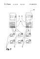
- FIG. 3 is a schematic diagram of a LAN including a server equipped with a communications device in accordance with the present invention.
- FIG. 4 is a front view of the communications device as shown in FIG. 3 .
- FIG. 5 is a rear view of the communications device as shown FIG. 3, with the rear housing portion removed.
- FIG. 6 is a fragmentary side view of the communications device as shown in FIG. 3 .
- FIG. 7 is a greatly enlarged cross-sectional view of the circuit board in the communications device as shown in FIG. 3 .
- FIG. 8 is a schematic diagram of a second embodiment of the communications device in accordance with the present invention.
- FIG. 9 is a schematic diagram of a third embodiment of a communications device in accordance with the present invention.
- the communications device 35 may advantageously be incorporated into a server 33 , which, in turn, is part of a LAN 30 .
- the LAN 30 interconnects a plurality of user workstations 31 .
- Twisted pair lines 32 may connect the workstations 31 to the respective ports of the respective communications devices 35 .
- fiber cables may be used to connect the workstations, or a mixture of fiber and twisted pair lines may be used.
- the communications device 35 is shown incorporated into a server 33 , it may also be advantageously be incorporated in other computer devices.
- the communications device 35 may be used, for example, in an integrated cable TV modem and Ethernet hub, as will also be readily appreciated by those skilled in the art. Other applications are also contemplated by the invention.
- the communications device 35 includes multi-port jack housing 36 having a front and a back, and including portions defining a plurality of recesses 37 extending inwardly from the front for receiving respective mating plugs, not shown.
- the multi-port jack housing 36 may be integrally molded plastic, for example, as will be readily understood by those skilled in the art.
- six recesses 37 are positioned in side-by-side relation, and two tiers of such recesses are provided. Any number of recesses 37 may be provided as explained in greater detail below.
- the illustrated twelve-port arrangement provides a relatively compact, yet readily manufactured embodiment of the communications device 35 . This arrangement provides a relatively high port density and is also rugged and reliable when formed using conventional plastic molding techniques.
- Signal connector means are preferably positioned within each of the recesses 37 and define a respective plurality of communications ports 38 .
- a plurality of biased electrical contacts 41 are provided.
- the arrangement of the contacts 41 and the size and configuration of the recesses 37 are compatible with the ubiquitous RJ-45 jack, which is commonly used in LAN and other communications applications as will be readily understood by those skilled in the art.
- Other configurations of electrical contacts are also contemplated by the present invention.
- Each communications port 38 establishes inbound and outbound signal paths with a respective mating plug.
- a relatively compact circuit board 45 is illustratively positioned within the multi-port jack housing 36 and extends across the entire back thereof as shown best in FIG. 5 .
- the communications device 35 includes three communications processors 42 mounted on the circuit board and connected to the plurality of communications ports 38 for processing inbound and outbound communications signals.
- Each communications processor 42 communicates with four communications ports 38 in the illustrated embodiment. In other embodiments, other numbers of ports 38 can be handled by each processor. Accordingly, an extremely compact multi-port device is provided.
- Each communications processor 42 may be provided, for example, by a commercially available integrated circuit offered by Level One under the designation LXT915.
- the communications processor 42 includes a plurality of transceivers for a corresponding group of communications ports 38 .
- ICs were positioned on relatively large and bulky mother boards as part of a hub as described above in the Background of the Invention section.
- the considerable signal processing capability of the IC is provided within the compact multi-port housing 36 .
- the communications device 35 may be connected to a mother circuit board, such as of the server 33 (FIG. 3 ), or other similar computer device. A separate hub may then not be needed.
- the initial purchase cost, and maintenance costs may be less.
- the LAN 30 will be simpler and more robust.
- the communications processors 42 are shown as integrated circuit packages, that is, with an integrally molded layer and outwardly extending leads, the processors may also be provided by the individual circuit die without the package.
- the circuit board 45 may mount the individual integrated circuit die as will be readily appreciated by those skilled in the art. Mounting the individual circuit die requires considerable less surface area on the circuit board 45 , which is necessarily relatively limited because of the compact dimensions of the multi-port housing 36 to be compatible with the RJ-45 jacks.
- a plurality of pins 46 extend outwardly from the bottom edge of the circuit board 45 as shown in FIG. 5 . These pins 46 can be inserted into corresponding openings in a circuit board to which the communications device 35 is attached, such as the mother board of the server.
- the communications device 35 also illustratively includes a metal or other conductive layer 47 which covers the outer surface portions of the multi-port housing 36 to thereby provide an EMI shield. Accordingly, adjacent components will not interfere with the circuitry within the housing 36 , and conversely, EMI will not be radiated outwardly from the housing.
- a back panel covers the circuit board 45 .
- the outer EMI shield 47 would also include portions which cover the back panel.
- the circuit board 45 illustratively comprises an electrically conductive layer 51 between two dielectric layers 52 .
- the electrically conductive layer 51 defines an internal electromagnetic interference (EMI) shield.
- the electrically conductive layer 47 which defines the external EMI shield may be connected to the electrically conductive layer 51 which defines the internal EMI shield.
- EMI electromagnetic interference
- the processors 42 are positioned adjacent the back of the multi-port housing 36 . The position could be reversed in other embodiments.
- EMI generating devices such as the illustrated circuit magnetics 54
- the magnetics 54 or other EMI generating devices are preferably on the opposite side from the processor. Accordingly, a compact arrangement is facilitated without compromising performance caused by EMI.
- a second embodiment of the communications device 35 ′ is schematically illustrated in FIG. 8 .
- the communications processor 42 ′ is connected to four transceivers 56 ′.
- the transceivers 56 ′ may be part of the integrated circuit of the processor.
- Magnetics 54 ′ are provided for interfacing the twisted pair ports 38 ′.
- Optical interfaces 57 ′ are provided for interfacing the transceivers 56 ′ to the optical ports 55 ′.
- each such port includes an optical detector 61 ′ for inbound optical signals and an optical emitter 62 ′ for outbound optical signals.
- the optical detector 61 ′ and optical emitter 62 ′ provide the signal connector means.
- This second embodiment illustrates a mix of both optical and twisted pair ports, and those of skill in the art will recognize that the ports can also be all optical or all twisted pair, for example, in other embodiments.
- the optical detector 61 ′ and optical emitter 62 ′ may be provided by any of a number of commercially available devices as will be readily appreciated by those skilled in the art.
- the communications device 35 ′ includes a multi-port housing 36 ′, circuit board mounting arrangement, and EMI shields as described above with reference to the embodiment as shown in FIGS. 3-7.
- a third embodiment of the communications device 35 ′′ is explained with additional reference to FIG. 9 .
- two communications processors 42 ′′ are provided.
- an internal repeater bus 66 ′′ is provided for communications between the two processors 42 ′′.
- the internal repeater bus 66 ′′ is provided by appropriate traces on the circuit board, for example, as will be readily appreciated by those skilled in the art.
- the communications processors 42 ′′ include circuitry for communicating with each other over this bus as will also be readily appreciated by those skilled in the art.
- each of the processors 42 ′′ is illustrated with transceiver circuitry 56 ′′ for each port, as well as PHY circuitry portions 65 ′′ for each group of four ports 38 ′′.
- the PHY circuitry portions 65 ′′ provide the so-called physical layer interface to the associated computer or other equipment.
- the communications device 35 ′′ includes a multi-port housing 36 ′′, circuit board mounting arrangement, and EMI shields as described above with reference to the embodiment described above.
- the circuitry mounted within the compact multi-port housing 36 ′′ performs the following functions: encodes and serializes the outgoing data, decodes and deserializes the incoming data, and synchronizes data flowing to and from the ports to the system bus timing.
- Another aspect of the invention relates to a method for making a communications device 35 comprising a multi-port jack housing 36 having a front and a back, and including portions defining a plurality of recesses 37 extending inwardly from the front for receiving respective mating plugs therein.
- the method preferably comprises the steps of: positioning signal connector means within each of the recesses 37 and defining a respective plurality of communications ports 38 , each communications port for establishing inbound and outbound signal paths with a respective mating plug; mounting at least one communications processor 42 on a circuit board 45 and connected to the plurality of communications ports for processing inbound and outbound communications signals; and positioning the circuit board within the multi-port jack housing and extending adjacent the back thereof.
Abstract
Description
Claims (62)
Priority Applications (5)
| Application Number | Priority Date | Filing Date | Title |
|---|---|---|---|
| US09/137,407 US6308235B1 (en) | 1998-06-16 | 1998-08-20 | Multi-port communications device and associated methods |
| US09/333,334 US6324610B1 (en) | 1998-06-16 | 1999-06-15 | Shared multi-port communications device and associated methods |
| AU45685/99A AU4568599A (en) | 1998-06-16 | 1999-06-15 | Multi-port communications device and associated methods |
| US09/333,462 US6344969B1 (en) | 1998-06-16 | 1999-06-15 | Switched multi-port communications device and associated methods |
| PCT/US1999/013491 WO1999066604A1 (en) | 1998-06-16 | 1999-06-15 | Multi-port communications device and associated methods |
Applications Claiming Priority (2)
| Application Number | Priority Date | Filing Date | Title |
|---|---|---|---|
| US09/098,277 US6497588B1 (en) | 1998-06-16 | 1998-06-16 | Communications transceiver with internal EMI shield and associated methods |
| US09/137,407 US6308235B1 (en) | 1998-06-16 | 1998-08-20 | Multi-port communications device and associated methods |
Related Parent Applications (2)
| Application Number | Title | Priority Date | Filing Date |
|---|---|---|---|
| US09/098,277 Continuation US6497588B1 (en) | 1998-06-16 | 1998-06-16 | Communications transceiver with internal EMI shield and associated methods |
| US09/098,277 Continuation-In-Part US6497588B1 (en) | 1998-06-16 | 1998-06-16 | Communications transceiver with internal EMI shield and associated methods |
Related Child Applications (2)
| Application Number | Title | Priority Date | Filing Date |
|---|---|---|---|
| US09/333,462 Continuation US6344969B1 (en) | 1998-06-16 | 1999-06-15 | Switched multi-port communications device and associated methods |
| US09/333,334 Continuation US6324610B1 (en) | 1998-06-16 | 1999-06-15 | Shared multi-port communications device and associated methods |
Publications (1)
| Publication Number | Publication Date |
|---|---|
| US6308235B1 true US6308235B1 (en) | 2001-10-23 |
Family
ID=26794585
Family Applications (3)
| Application Number | Title | Priority Date | Filing Date |
|---|---|---|---|
| US09/137,407 Expired - Fee Related US6308235B1 (en) | 1998-06-16 | 1998-08-20 | Multi-port communications device and associated methods |
| US09/333,334 Expired - Fee Related US6324610B1 (en) | 1998-06-16 | 1999-06-15 | Shared multi-port communications device and associated methods |
| US09/333,462 Expired - Fee Related US6344969B1 (en) | 1998-06-16 | 1999-06-15 | Switched multi-port communications device and associated methods |
Family Applications After (2)
| Application Number | Title | Priority Date | Filing Date |
|---|---|---|---|
| US09/333,334 Expired - Fee Related US6324610B1 (en) | 1998-06-16 | 1999-06-15 | Shared multi-port communications device and associated methods |
| US09/333,462 Expired - Fee Related US6344969B1 (en) | 1998-06-16 | 1999-06-15 | Switched multi-port communications device and associated methods |
Country Status (2)
| Country | Link |
|---|---|
| US (3) | US6308235B1 (en) |
| AU (1) | AU4568599A (en) |
Cited By (8)
| Publication number | Priority date | Publication date | Assignee | Title |
|---|---|---|---|---|
| US20020188709A1 (en) * | 2001-05-04 | 2002-12-12 | Rlx Technologies, Inc. | Console information server system and method |
| US20020188718A1 (en) * | 2001-05-04 | 2002-12-12 | Rlx Technologies, Inc. | Console information storage system and method |
| US20040059850A1 (en) * | 2002-09-19 | 2004-03-25 | Hipp Christopher G. | Modular server processing card system and method |
| US6985967B1 (en) * | 2000-07-20 | 2006-01-10 | Rlx Technologies, Inc. | Web server network system and method |
| US7044777B1 (en) | 2002-01-31 | 2006-05-16 | Methode Electronics, Inc. | Multi-port module receptacle |
| US20070015416A1 (en) * | 2005-03-23 | 2007-01-18 | Gutierrez Aurelio J | Power-enabled connector assembly and method of manufacturing |
| US7300215B2 (en) | 2004-06-04 | 2007-11-27 | Industrial Technology Research Institute | Light transceiver module |
| EP2538500A1 (en) * | 2011-06-22 | 2012-12-26 | Phoenix Contact GmbH & Co. KG | Coupling device for communication devices |
Families Citing this family (9)
| Publication number | Priority date | Publication date | Assignee | Title |
|---|---|---|---|---|
| US6431764B1 (en) * | 1998-06-16 | 2002-08-13 | Stratos Lightwave | Optical transceiver RJ-jack with EMI shield |
| US20020042857A1 (en) * | 2000-10-05 | 2002-04-11 | Jones Nicolas D.L. | Industrial multi-port data connector system |
| US6450837B1 (en) * | 2001-10-29 | 2002-09-17 | Hon Hai Precision Ind. Co., Ltd. | Electrical connector having surge suppressing device |
| US7323882B1 (en) * | 2003-05-14 | 2008-01-29 | Pent Technologies, Inc. | System to place receptacles and distribution blocks |
| TW200529498A (en) * | 2004-02-24 | 2005-09-01 | Delta Electronics Inc | Connector module |
| US6945820B1 (en) * | 2004-11-15 | 2005-09-20 | Hon Hai Precision Ind. Co., Ltd. | Electrical connect having integrated over current protector |
| US7690849B2 (en) * | 2007-05-16 | 2010-04-06 | Protokraft, Llc | Fiber optic connector, active contact inserts therefor, and associated methods |
| US7845984B2 (en) * | 2008-07-01 | 2010-12-07 | Pulse Engineering, Inc. | Power-enabled connector assembly and method of manufacturing |
| WO2017131694A1 (en) | 2016-01-28 | 2017-08-03 | Hewlett Packard Enterprise Development Lp | Printed circuit boards |
Citations (13)
| Publication number | Priority date | Publication date | Assignee | Title |
|---|---|---|---|---|
| US4973799A (en) * | 1988-09-02 | 1990-11-27 | Konica Corporation | Printed circuit board for use with an image forming apparatus |
| US5280598A (en) * | 1990-07-26 | 1994-01-18 | Mitsubishi Denki Kabushiki Kaisha | Cache memory and bus width control circuit for selectively coupling peripheral devices |
| US5518423A (en) | 1994-07-19 | 1996-05-21 | The Siemon Company | Shielded connector assembly |
| US5650917A (en) * | 1996-10-09 | 1997-07-22 | Hsu; Fu-Yu | CPU card mounting structure |
| US5841633A (en) * | 1997-09-16 | 1998-11-24 | Huang; Chuan-Wen | Cup and heat sink mounting arrangement |
| US5949648A (en) * | 1998-02-26 | 1999-09-07 | Compal Electronics Inc. | Heat radiating device capable of reducing electromagnetic interference |
| US5969946A (en) * | 1996-12-24 | 1999-10-19 | Hon Hai Precision Ind. Co., Ltd. | Heat dissipating electrical apparatus |
| US5982634A (en) * | 1996-11-14 | 1999-11-09 | Systran Corporation | High speed switch package provides reduced path lengths for electrical paths through the package |
| US5986693A (en) * | 1997-10-06 | 1999-11-16 | Adair; Edwin L. | Reduced area imaging devices incorporated within surgical instruments |
| US5991837A (en) * | 1997-12-02 | 1999-11-23 | Micron Electronics, Inc. | Reverse oriented processor configuration |
| US6061238A (en) * | 1998-06-29 | 2000-05-09 | Hitachi, Ltd. | Information processing apparatus, method of arranging components of the apparatus, and heat sink |
| US6094344A (en) * | 1995-10-13 | 2000-07-25 | Hitachi, Ltd. | Heat dissipation structure for a personal computer including two heat dissipation block assemblies and two heat dissipation plates |
| US6115755A (en) * | 1998-04-09 | 2000-09-05 | Novaweb Technologies, Inc. | Integrated apparatus for interfacing several computers to the internet through a single connection |
Family Cites Families (4)
| Publication number | Priority date | Publication date | Assignee | Title |
|---|---|---|---|---|
| JPH0798620A (en) * | 1992-11-13 | 1995-04-11 | Seiko Epson Corp | Electronic device and computer using it |
| US5647767A (en) | 1995-02-06 | 1997-07-15 | The Whitaker Corporation | Electrical connector jack assembly for signal transmission |
| US5876240A (en) * | 1997-04-01 | 1999-03-02 | The Whitaker Corp | Stacked electrical connector with visual indicators |
| US5915993A (en) * | 1997-02-27 | 1999-06-29 | Berg Technology, Inc. | Assembly containing a modular jack and a light emitting diode |
-
1998
- 1998-08-20 US US09/137,407 patent/US6308235B1/en not_active Expired - Fee Related
-
1999
- 1999-06-15 US US09/333,334 patent/US6324610B1/en not_active Expired - Fee Related
- 1999-06-15 AU AU45685/99A patent/AU4568599A/en not_active Abandoned
- 1999-06-15 US US09/333,462 patent/US6344969B1/en not_active Expired - Fee Related
Patent Citations (13)
| Publication number | Priority date | Publication date | Assignee | Title |
|---|---|---|---|---|
| US4973799A (en) * | 1988-09-02 | 1990-11-27 | Konica Corporation | Printed circuit board for use with an image forming apparatus |
| US5280598A (en) * | 1990-07-26 | 1994-01-18 | Mitsubishi Denki Kabushiki Kaisha | Cache memory and bus width control circuit for selectively coupling peripheral devices |
| US5518423A (en) | 1994-07-19 | 1996-05-21 | The Siemon Company | Shielded connector assembly |
| US6094344A (en) * | 1995-10-13 | 2000-07-25 | Hitachi, Ltd. | Heat dissipation structure for a personal computer including two heat dissipation block assemblies and two heat dissipation plates |
| US5650917A (en) * | 1996-10-09 | 1997-07-22 | Hsu; Fu-Yu | CPU card mounting structure |
| US5982634A (en) * | 1996-11-14 | 1999-11-09 | Systran Corporation | High speed switch package provides reduced path lengths for electrical paths through the package |
| US5969946A (en) * | 1996-12-24 | 1999-10-19 | Hon Hai Precision Ind. Co., Ltd. | Heat dissipating electrical apparatus |
| US5841633A (en) * | 1997-09-16 | 1998-11-24 | Huang; Chuan-Wen | Cup and heat sink mounting arrangement |
| US5986693A (en) * | 1997-10-06 | 1999-11-16 | Adair; Edwin L. | Reduced area imaging devices incorporated within surgical instruments |
| US5991837A (en) * | 1997-12-02 | 1999-11-23 | Micron Electronics, Inc. | Reverse oriented processor configuration |
| US5949648A (en) * | 1998-02-26 | 1999-09-07 | Compal Electronics Inc. | Heat radiating device capable of reducing electromagnetic interference |
| US6115755A (en) * | 1998-04-09 | 2000-09-05 | Novaweb Technologies, Inc. | Integrated apparatus for interfacing several computers to the internet through a single connection |
| US6061238A (en) * | 1998-06-29 | 2000-05-09 | Hitachi, Ltd. | Information processing apparatus, method of arranging components of the apparatus, and heat sink |
Non-Patent Citations (4)
| Title |
|---|
| Data Sheet LXT915, "Simple Quad Ethernet Repeater", Level One, (Apr. 1997), pp. 1-21. |
| Product Sheet H309.A, "Fastpulse High Speed LAN Transceivers", Pulse, (Jul. 1996), pp. 1-4. |
| Product Sheet MD6301 Series, "Single 10/100BASE-TX Filtered Connector Module", Valor Electronics, Inc., 1997. |
| Product Sheet MD6304 Series, "Quad 10/100BASE-TX Filtered Connector Module", Valor Electronics, Inc., 1997. |
Cited By (12)
| Publication number | Priority date | Publication date | Assignee | Title |
|---|---|---|---|---|
| US6985967B1 (en) * | 2000-07-20 | 2006-01-10 | Rlx Technologies, Inc. | Web server network system and method |
| US20020188709A1 (en) * | 2001-05-04 | 2002-12-12 | Rlx Technologies, Inc. | Console information server system and method |
| US20020188718A1 (en) * | 2001-05-04 | 2002-12-12 | Rlx Technologies, Inc. | Console information storage system and method |
| US7044777B1 (en) | 2002-01-31 | 2006-05-16 | Methode Electronics, Inc. | Multi-port module receptacle |
| US20060211302A1 (en) * | 2002-01-31 | 2006-09-21 | Daly John J | Multi-port module receptacle |
| US7275959B2 (en) | 2002-01-31 | 2007-10-02 | Methode Electronics, Inc. | Multi-port module receptacle |
| US20040059850A1 (en) * | 2002-09-19 | 2004-03-25 | Hipp Christopher G. | Modular server processing card system and method |
| US7300215B2 (en) | 2004-06-04 | 2007-11-27 | Industrial Technology Research Institute | Light transceiver module |
| US7680389B2 (en) | 2004-06-04 | 2010-03-16 | Industrial Technology Research Institute | Light transceiver module |
| US20070015416A1 (en) * | 2005-03-23 | 2007-01-18 | Gutierrez Aurelio J | Power-enabled connector assembly and method of manufacturing |
| US7524206B2 (en) | 2005-03-23 | 2009-04-28 | Pulse Engineering, Inc. | Power-enabled connector assembly with heat dissipation apparatus and method of manufacturing |
| EP2538500A1 (en) * | 2011-06-22 | 2012-12-26 | Phoenix Contact GmbH & Co. KG | Coupling device for communication devices |
Also Published As
| Publication number | Publication date |
|---|---|
| AU4568599A (en) | 2000-01-05 |
| US6324610B1 (en) | 2001-11-27 |
| US6344969B1 (en) | 2002-02-05 |
Similar Documents
| Publication | Publication Date | Title |
|---|---|---|
| US6308235B1 (en) | Multi-port communications device and associated methods | |
| US5639266A (en) | High frequency electrical connector | |
| US9876322B2 (en) | Backward compatible connectivity for high data rate applications | |
| JP5377512B2 (en) | Method and system for reducing common mode signal generation in plug / jack connections | |
| CA2347985C (en) | Crosstalk compensation for electrical connectors | |
| US6062908A (en) | High density connector modules having integral filtering components within repairable, replaceable submodules | |
| US7052328B2 (en) | Electronic connector and method of performing electronic connection | |
| US7568950B2 (en) | High speed modular jack including multiple contact blocks and method for assembling same | |
| WO1998033242A9 (en) | High density connector modules having integral filtering components within repairable, replaceable submodules | |
| US5340333A (en) | Shielded modular adapter | |
| US6165018A (en) | Connector having internal crosstalk compensation | |
| US6497588B1 (en) | Communications transceiver with internal EMI shield and associated methods | |
| US6945820B1 (en) | Electrical connect having integrated over current protector | |
| US6431764B1 (en) | Optical transceiver RJ-jack with EMI shield | |
| US10559927B2 (en) | Switchable RJ45/ARJ45 jack | |
| US7361053B1 (en) | Network element connector assembly including stacked connector interfaces | |
| WO1999066604A1 (en) | Multi-port communications device and associated methods | |
| WO2015054566A1 (en) | Switchable rj45/arj45 jack | |
| EP1432078A1 (en) | Cable connector shell | |
| GB2382236A (en) | RJ jack with integerated interface magnetics |
Legal Events
| Date | Code | Title | Description |
|---|---|---|---|
| AS | Assignment |
Owner name: POLYCORE TECHNOLOGIES, FLORIDA Free format text: ASSIGNMENT OF ASSIGNORS INTEREST;ASSIGNORS:SCHARF, ROBERT M.;LORD, RANDAL B.;REEL/FRAME:009408/0557;SIGNING DATES FROM 19970817 TO 19970818 |
|
| AS | Assignment |
Owner name: STRATOS MICRO SYSTEMS, INC., FLORIDA Free format text: ASSIGNMENT OF ASSIGNORS INTEREST;ASSIGNOR:METHODE ELECTRONICS OF FLORIDA, INC.;REEL/FRAME:010959/0031 Effective date: 19990915 Owner name: METHODE COMMUNICATIONS MODULES, INC., FLORIDA Free format text: ASSIGNMENT OF ASSIGNORS INTEREST;ASSIGNOR:METHODE ELECTRONICS OF FLORIDA, INC.;REEL/FRAME:010959/0031 Effective date: 19990915 |
|
| AS | Assignment |
Owner name: METHODE FLORIDA, INC., FLORIDA Free format text: ASSIGNMENT AND CHANGE OF NAME;ASSIGNOR:POLYCORE TECHNOLOGIES, INC.;REEL/FRAME:010978/0560 Effective date: 19990414 Owner name: METHODE COMMUNICATION MODULES, INC., FLORIDA Free format text: ASSIGNMENT AND CHANGE OF NAME;ASSIGNOR:POLYCORE TECHNOLOGIES, INC.;REEL/FRAME:010978/0560 Effective date: 19990414 Owner name: STRATOS MICRO SYSTEMS, INC., FLORIDA Free format text: ASSIGNMENT AND CHANGE OF NAME;ASSIGNOR:POLYCORE TECHNOLOGIES, INC.;REEL/FRAME:010978/0560 Effective date: 19990414 |
|
| FPAY | Fee payment |
Year of fee payment: 4 |
|
| FPAY | Fee payment |
Year of fee payment: 8 |
|
| REMI | Maintenance fee reminder mailed | ||
| LAPS | Lapse for failure to pay maintenance fees | ||
| STCH | Information on status: patent discontinuation |
Free format text: PATENT EXPIRED DUE TO NONPAYMENT OF MAINTENANCE FEES UNDER 37 CFR 1.362 |
|
| FP | Lapsed due to failure to pay maintenance fee |
Effective date: 20131023 |