US6305000B1 - Placement of conductive stripes in electronic circuits to satisfy metal density requirements - Google Patents
Placement of conductive stripes in electronic circuits to satisfy metal density requirements Download PDFInfo
- Publication number
- US6305000B1 US6305000B1 US09/334,171 US33417199A US6305000B1 US 6305000 B1 US6305000 B1 US 6305000B1 US 33417199 A US33417199 A US 33417199A US 6305000 B1 US6305000 B1 US 6305000B1
- Authority
- US
- United States
- Prior art keywords
- design
- fill
- conductive fill
- power distribution
- conductive
- Prior art date
- Legal status (The legal status is an assumption and is not a legal conclusion. Google has not performed a legal analysis and makes no representation as to the accuracy of the status listed.)
- Expired - Lifetime
Links
Images


Classifications
-
- G—PHYSICS
- G06—COMPUTING; CALCULATING OR COUNTING
- G06F—ELECTRIC DIGITAL DATA PROCESSING
- G06F30/00—Computer-aided design [CAD]
- G06F30/30—Circuit design
- G06F30/39—Circuit design at the physical level
-
- H—ELECTRICITY
- H01—ELECTRIC ELEMENTS
- H01L—SEMICONDUCTOR DEVICES NOT COVERED BY CLASS H10
- H01L23/00—Details of semiconductor or other solid state devices
- H01L23/52—Arrangements for conducting electric current within the device in operation from one component to another, i.e. interconnections, e.g. wires, lead frames
- H01L23/522—Arrangements for conducting electric current within the device in operation from one component to another, i.e. interconnections, e.g. wires, lead frames including external interconnections consisting of a multilayer structure of conductive and insulating layers inseparably formed on the semiconductor body
- H01L23/528—Geometry or layout of the interconnection structure
- H01L23/5286—Arrangements of power or ground buses
-
- H—ELECTRICITY
- H01—ELECTRIC ELEMENTS
- H01L—SEMICONDUCTOR DEVICES NOT COVERED BY CLASS H10
- H01L2924/00—Indexing scheme for arrangements or methods for connecting or disconnecting semiconductor or solid-state bodies as covered by H01L24/00
- H01L2924/0001—Technical content checked by a classifier
- H01L2924/0002—Not covered by any one of groups H01L24/00, H01L24/00 and H01L2224/00
Definitions
- This invention relates generally to the design and manufacture of electronic circuits and more particularly relates to the addition of conductive fill stripes to satisfy metal density requirements and improve circuit performance.
- Electronic circuits comprise layers of semiconductor materials doped with specific elements or combination of elements to make them more or less conductive. It is the predictable and controlled movement of electrons or holes through these semiconductor materials that enable logic to be manipulated in transistors and other integrated devices.
- electronic circuits in microprocessors and computers are nothing more than multitudes of these integrated logic and storage devices interconnected with each other. These integrated devices are interconnected in electronic circuits with each other using metal layers in horizontal planes above the integrated devices. These metal layers, up to eight or more, are referred to M 1 , M 2 , M 3 , etc. have signal routing and power distribution on them. These metal layers are not necessarily identical to each other.
- design space which is nothing more than the set of possible designs and design parameters that meet a specific product requirement. Exploring design space means evaluating the various design options possible with a given technology and optimizing with respect to specific constraints such as power or cost. For a particular semiconductor process technology, such as 0.5 micron CMOS, there are corresponding design rules that state the allowable limits for feature size, feature separation, layer-to-layer overlap, layer-to-layer feature separation, etc. used in the design and layout of integrated circuits. After an integrated circuit has been designed, the design is checked for compliance with the constraints imposed by these design rules, usually by a computerized design rule checker (DRC).
- DRC computerized design rule checker
- Silicon technology and integrated circuits have evolved to a point where the geometry of transistors and wires are so small with an increase in corresponding circuit density that it is becoming increasingly difficult to manufacture silicon chips with good yield and tolerances. Copper technology is especially sensitive to manufacturing process variations because of its smaller size.
- the design rules of manufacturers require that all wiring levels on these electronic circuits have a minimum usage requirement, i.e., a minimum density of metal per area, across all portions of the circuit to achieve consistent metal distribution across a wafer to improve manufacturing yield and reliability. For instance, one of these design rules for silicon technology require that all metal levels from M 1 to M 5 have a minimum density requirement of twenty percent or larger per area of one hundred square microns. The minimum density requirement for the thicker metal levels are ten percent or larger per one hundred square microns area.
- FIG. 1 is a layout of conductors, also called buses, of two metal layers of an electronic circuit 10 .
- Metal layer M 2 has power distribution and signal routing in which the power distribution comprise ground conductors 210 a and 210 b, bias voltage conductor 230 a, and signal routing 270 a, 270 b, . . . 270 f . . . 270 z.
- Another metal layer M 3 lies in a plane above the first metal layer M 2 with conductors running perpendicularly to those conductors in metal layer M 2 .
- Metal layer M 3 shows power distribution comprising ground conductors 310 a and 310 b and a bias voltage conductor 330 a.
- the layout of the power distribution and signal routing of the electronic circuit 10 of FIG. 1 is considered ideal because the ground conductors are equally spaced from the bias voltage conductors and because the signal routing is equally spaced and uniformly interspersed among the power distribution.
- the conductors of the power distribution are ideally the same size, as are the signal routing albeit a different size than the ground and voltage conductors. When bias voltages are applied to the conductors and when signals are routed through the signal routing, the power and resultant heating will be equally dissipated over the area of the electronic circuit 10 of FIG. 1 .
- FIG. 2 illustrates a more realistic electronic circuit 20 having two metal layers M 2 and M 3 positioned one above the other with the power distribution and signal routing as shown in FIG. 1 with the exception that there are fewer signal conductors in metal layer M 2 .
- metal layer M 2 In the M 2 layer of FIG. 2, there are only three signal conductors 270 c, 270 f, and 270 z.
- FIG. 2 there are empty regions 11 , 13 , 15 , 17 , and 19 between the power distribution conductors of both the M 2 and M 3 layers and the signal routing 270 c, 270 f, and 270 z. These empty regions 11 , 13 , 15 , 17 , and 19 violate the minimum area usage requirement for metal, especially in sensitive copper technologies as mentioned.
- the design rules and the manufacturing processes require that the empty regions 11 , 13 , 15 , 17 , and 19 be filled with metal or other conductors to satisfy a particular minimum usage requirement. In actuality, however, meeting the design rules is not as easy as placing conductors at regular intervals in a metal layer as shown in FIG. 1 .
- Some logic or storage devices are busier than others, some devices require larger operating bias voltages, etc.
- some areas of the electronic circuit are more dense and consume more power and/or generate more signals than other areas of the electronic circuit.
- FIG. 3 illustrates the layout of two metal layers M 2 and M 3 of FIG. 2 but empty regions 11 , 13 , 15 , 17 , and 19 and other empty regions have been filled with small floating metal conductors labeled 240 a, 240 b, 240 c . . . 240 q in the M 2 layer using the sprinkle fill approach.
- these metal fills are floating, i.e., they are not electrically connected to either the power distribution or the signal routing.
- An electronic circuit comprises a plurality of integrated circuits on a wafer with a plurality of metal conductive layers each having a distribution network of power and signal conductors with empty areas there between, the plurality of metal conductive layers being electrically connected to the integrated circuits.
- a plurality of conductive fill stripes are placed in the design of the electronic circuit in the empty areas to meet metal density requirements of the electronic circuit.
- the conductive fill stripes are electrically connected to the distribution network. It is envisioned that the power distribution, the signal conductors, and the conductive fill stripes could be of copper, titanium, aluminum, gold, tungsten, or any alloy thereof.
- the conductive fill stripes are preferably positioned between the signal conductors and the power distribution on the same metal conductive layer.
- the power distribution may further comprise a ground power bus and a bias voltage bus wherein at least one of the conductive fill stripes is electrically connected to a ground power bus or a bias voltage bus on an adjacent metal conductive layer.
- the ground fill stripe may be electrically connected to a ground power bus on the same as or different metal conductive layer than the bias voltage bus to which a bias voltage fill stripe on the intermediate metal layer is electrically connected.
- Some of the conductive fill stripes may be electrically connected to signal routing on an adjacent metal conductive layer.
- Another embodiment of the invention can be considered an electronic circuit having a plurality of integrated circuits on a wafer, a plurality of metal conductive layers one above another with the conductive layers being electrically connected to the integrated circuits and to each other.
- Each of the metal conductive layers have a distribution network of ground power buses and bias voltage power buses and signal routing.
- the conductive fill stripes may be at least one ground fill stripe parallel to and coextensive with the distribution network of its own metal conductive layer and electrically connected to a ground power bus on a first adjacent metal conductive layer.
- the conductive fill stripe may also be at least one bias voltage fill stripe parallel to and coextensive with the distribution network of its own metal conductive layer and electrically connected to a bias voltage power bus on a second adjacent metal conductive layer.
- a method which comprises the steps of defining power distribution, external IO signal routing, acceptable circuit placements and internal signal routing of the design. Circuits and interconnections between the circuits are placed on the design and a map of the power distribution and the external and internal signal routing is added onto the design. Conductive fill striping is added to portions of the map of the design which do not satisfy metal density requirements. The maximum amount of conductive fill striping to can be added to those portions, or conductive fill striping may be added to portions of the only if a distance to the power distribution or the signal routing is greater than or equal to a specified spacing variable of a design rule.
- the conductive fill striping is connected to the power distribution in the design and those conductive fill striping cannot be electrically connected to said power distribution are deleted from the design.
- a design rule checker is run to determine if the design satisfies design rules and meets metal density requirements. If not, more conductive fill stripes are added to the design and the process is repeated until the design meets the metal density requirements. The logical function of the design is verified against an electrical schematic of the design and the method determines that the conductive fill striping can be electrically connected to said power distribution in the design.
- the method to design electronic circuits may comprise the steps of defining power distribution, external IO signal routing, acceptable circuit placements and internal signal routing of the design.
- Preferred locations in the design for the placement of conductive fill striping based on power distribution and signal strength and switching speed of signal routing are predefined in the process.
- the circuits and a plurality of interconnections between said circuits are placed on the design.
- the conductive fill striping is added in the design to those predefined preferred locations lacking signal routing and are connected to the power distribution.
- the conductive fill striping that cannot be electrically connected to the power distribution is deleted and a design rule checker is run to determine if said design satisfies design rules.
- conductive fill striping is including in the design in those locations and the process repeats. If, however, the design meets the metal density requirements then the logical function of the design is verified against an electrical schematic and it is determined that the conductive fill striping can actually be electrically connected to the power distribution in the design.
- FIG. 1 is an illustration of a layout of power and signal conductors of two metal layers in an ideal electronic circuit.
- FIG. 2 is an illustration of a layout of power and signal conductors of two metal layers in a prior art electronic circuit.
- FIG. 3 is an illustration of the placement of metal conductors sprinkled into spaces between power and signal conductors in a prior art electronic circuit of FIG. 2 .
- FIG. 4 is an illustration of the placement of conductive striping in an electronic circuit in accordance with an embodiment of the invention. It is recommended that FIG. 4 be printed on the face of the patent.
- FIG. 5 is a vertical cross-section of the right edge of the electronic circuit of FIG. 4 .
- FIGS. 6 a and 6 b illustrate capacitive coupling between conductors in the same plane of the prior art electronic circuit sprinkled with metal fill, and of the electronic circuit using conductive striping in accordance with an embodiment of the invention, respectively.
- FIGS. 7 a and 7 b illustrate capacitive coupling between metal layers of the prior art electronic circuit sprinkled with metal fill, and of the electronic circuit using conductive striping in accordance with an embodiment of the invention, respectively.
- FIGS. 8 a and 8 b illustrate a horizontal view and a vertical cross section, respectively, of a signal net incorporated into a metal layer of the prior art electronic circuit.
- FIGS. 9 a and 9 b illustrate a horizontal view and a vertical cross section, respectively, of a signal net incorporated in a metal layer of an electronic circuit according to an embodiment of the invention.
- FIG. 10 is a simplified flow chart of a process to incorporate conductive fill stripes into the design of an electronic circuit according to one embodiment of the invention.
- FIG. 11 is a simplified flow chart of a process to incorporate conductive fill stripes into the design of an electronic circuit according to another embodiment of the invention.
- FIG. 12 is a simplified flow chart of a process to verify the placement of conductive fill stripes into the design of an electronic circuit according to principles of the invention.
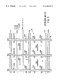
- FIG. 4 shows an embodiment of the invention to provide a more useful and robust approach to satisfy the integrated chip's metal area usage requirements by filling the unused area with conductive fill striping.
- FIG. 4 has the same basic layout of metal layers M 3 above metal layer M 2 with both layers having power distribution and signal routing as in FIG. 2 .
- Metal layer M 3 has ground buses 310 a and 310 b and bias voltage buses 330 a and 330 b.
- Metal layer M 2 has, from the top of the figure to bottom, a ground bus 210 a, a bias voltage conductor fill stripe 235 a (VDD FILL), a signal conductor 270 c, a ground conductor fill stripe 215 a (GND FILL), a second signal conductor 270 f, a second GND FILL 215 b, a bias voltage bus 230 a, a third GND FILL 215 c, another VDD FILL 235 b, a fourth GND FILL 215 d, another VDD FILL 235 c, a signal conductor 270 z, and a ground bus 210 b.
- VDD FILL bias voltage conductor fill stripe 235 a
- GND FILL ground conductor fill stripe 215 a
- second signal conductor 270 f a second GND FILL 215 b
- a bias voltage bus 230 a a third GND FILL 215 c, another VDD FILL 235 b
- This particular layout is somewhat arbitrary and should be considered as illustrative only; the particular layout is not intended to be limiting in any fashion.
- Metal layer M 3 is shown in FIG. 4 without any conductor fill stripes but in actuality, M 3 may also have a number of conductor fill stripes.
- the spacing and arrangement of the conductor fill stripes is also somewhat arbitrary in FIG. 4 meaning that two or more VDD FILL conductor stripes may be adjacent to each other or two or more GND FILL conductor stripes may be adjacent each other.
- the pattern of buses, signal conductors, and conductor fill stripes must be determined based on the individual applications and circuit parameters.
- Conductive fill stripes are not necessarily symmetric with respect to any ground or power bus and although there is a tendency to alternate GND FILL and VDD FILL conductor stripes, it need not be so.
- the conductive fill stripes may also be connected to signal routes, but it is preferred that the conductive fill strips be electrically connected to the power distribution.
- the conductive fill stripes 215 a, 215 b, 215 c, 215 d and 235 a, 235 b, and 235 c fill the empty spaces 11 , 13 , 15 , 17 , and 19 and other unlabeled open spaces to meet minimum conductor density requirements.
- the conductive fill stripes are preferably parallel to and coextensive with, i.e., the conductive fill stripes extend uninterrupted along the longer dimension, existing power buses in its own metal layer and perpendicular to power buses and signal routing in metal layers above or below and are electrically connected to them to enhance both layers.
- the conductive fill stripes extend uninterrupted along the longer dimension, existing power buses in its own metal layer and perpendicular to power buses and signal routing in metal layers above or below and are electrically connected to them to enhance both layers.
- FIG. 4 illustrates the interlevel connections 250 a, 250 b 250 c . . . 250 v which electrically connect a conductive fill stripe with its corresponding power bus.
- FIG. 5 is a vertical cross-section of the electronic circuit 40 from its right edge as shown in FIG. 4 .
- FIG. 5 shows three metal layers M 1 , M 2 , and M 3 each above the other. Layers M 2 and M 3 are the same layers as in FIG. 4, but metal layer M 1 is not visible in FIG. 4 because its view is blocked by metal layer M 3 .
- metal layer M 1 has a ground power bus 110 a under the bias voltage bus 330 b.
- Conductive bias voltage fill stripes VDD FILL 235 a, 235 b, and 235 c are electrically connected through interlevel connections 250 a, 250 c, and 250 d, respectively, to perpendicular bias voltage bus 330 b of metal layer M 3 .
- Conductive ground fill stripes GND FILL 215 a, 215 b, 215 c, and 215 d are electrically connected through interlevel connections 150 b, 150 c, 150 d, and 150 e to perpendicular ground power bus 110 a in metal layer M 1 .
- Interlevel connections are also provided for electrically connecting the power bus on one level with its corresponding power bus on another layer.
- ground power buses 210 a and 210 b on metal layer M 2 are electrically connected through interlevel connection 150 a and 150 f, respectively, to ground power bus 110 a on metal layer M 1 .
- bias voltage power bus 330 b on metal layer M 3 is electrically connected to bias voltage bus 230 a on metal layer M 2 at interlevel connection 250 b.
- FIGS. 6 a and 6 b are illustrations of coplanar capacitive coupling in the prior art using the floating metal fill as shown in FIG. 3 contrasted with using conductive fill stripe 215 a in accordance with one embodiment of the invention as shown in FIG. 4 .
- FIG. 6 a illustrates floating metal fill 240 d and 240 e between two signal wires 270 c and 270 f. Capacitive coupling which creates signal interference and reduces signal strength exists between the signal wires 270 c and 270 f and the metal floating fill 240 d and 240 e.
- Shown in FIG. 6 b is a conductive fill stripe 215 a GND FILL connected to a ground power bus. With the connected conductive fill stripe any coupling between the conductive fill stripe 215 a and signal wires 270 c and 270 f is grounded and the signal routing system becomes more robust.
- FIGS. 7 a and 7 b are illustrations of capacitive coupling between metal layer in the prior art using the floating metal fill 250 s contrasted with using conductive fill stripe 215 s in accordance with one embodiment of the invention.
- the conductive fill stripe 215 s reduces vertical coupling between metal layers.
- Shown in FIG. 7 a is a cross section of three metal layers M 1 , M 2 , and M 3 vertically displaced from each other.
- Layer M 1 has a signal wire 170 a extending horizontally across the figure.
- Layer M 2 in a horizontal plane above M 1 and below layer M 3 contains floating metal fill 240 s of the prior art.
- Layer M 3 has a plurality of signal wires 370 a - 370 f extending in a third dimension in and out of the page perpendicular to layers M 1 and M 2 .
- floating metal fill 240 s creates coupling between the signal wire 170 a in layer M 1 and signal wires 370 a - 370 f of layer M 3 .
- FIG. 7 b illustrates three metal layers M 1 , M 2 , and M 3 in a similar vertical arrangement as in FIG. 7 a.
- Layer M 2 between layers M 1 and layer M 3 has a GND FILL conductive power stripe 215 s although it could easily be a VDD FILL conductive stripe as well. Any capacitive coupling between the signal wires 370 a - 370 f in metal layer M 3 and signal wire 170 a in metal layer M 1 is grounded because GND FILL conductive power strip 215 s is electrically connected to a ground power bus (not shown). In this manner conductive fill stripes enhance signal strength and reduce noisy switching signals.
- FIG. 8 a is a simplified illustration of a prior art large input/output (IO) conductor 360 , also called a net, situated on metal layer M 3 of an electronic circuit 80 .
- IO input/output
- FIG. 8 b is a vertical cross-section of the arrangement of the upper-half of FIG.
- FIG. 9 a shows the same IO net 360 on metal layer M 3 .
- Metal layer M 2 now has conductive fill stripes 215 a , 215 b positioned below (FIG. 9 a ) and to the right (FIG. 9 b ) of each signal wire 270 c and 270 f.
- Conductive fill stripe 235 a is positioned above (FIG. 9 a ) and to the left (FIG. 9 b ) of signal wire 270 c.
- conductive fill stripes in this particular arrangement is not to be taken as limiting and it could easily have been a different number and conductive fill stripes that had been positioned differently around the signal wires.
- the conductive fill stripes are added to empty metal areas of the chip where the metal density does not meet manufacturing requirements, the conductive fill stripes are normally added so that at least a wiring track gap exists between the conductive fill stripe and a signal wire. This preferred placement limits any impact on active signal line capacitance. The flexibility to define how close or far away the conductive fill stripes are from the signal wires depends on the requirements of the area and signals involved.
- the conductive fill stripes be part of the power distribution and thus would be designed into the electronic circuit when the signal routing and the power distribution are designed after an area of the circuit is completed. In this fashion, the impact of including conductive fill stripes into the design can be assessed and necessary changes can be made earlier in the design and manufacturing process. Because the conductive fill stripes are part of the power distribution, moreover, DRC, LVS and extraction tools which generate electrical schematics from the layouts can assess whether the electronic circuit having the conductive fill stripes meet manufacturing density requirements and can detect any potential shorts, and can analyze noise and timing to obtain a more robust electronic circuit.
- FIG. 10 is a simplified flow chart of two options of an embodiment of the invention to add the conductive fill stripes during the design phase of an electronic circuit.
- Step 1010 begins a process during the design in which the power distribution and external IO signal routing are defined on the integrated circuit image. Then acceptable placements for circuits and the signal routing are set as in step 1020 .
- step 1030 the electronic circuits and the signal routing and power distribution and interconnections for circuits are placed in the design and in step 1040 a map of the signal routing signal conductors and power distribution for all metal layers is generated.
- there exist two options which use the same basic method, as in step 1050 for the placement of conductive fill stripes into the open areas.
- a second option of placing conductive fill stripes into an electronic circuit has as its upper bound adding maximum fill as above and as its lower bound adding no fill if the existing spacing meets the design rules. Conductive fill stripes are added to open areas only if a spacing to an adjacent conductor is greater than or equal to the specified spacing variable. Implementing a fill strategy of this sort provides more flexibility to accommodate manufacturing changes as well as the timing goal or other goals of a specific project. At step 1060 , conductor fill stripes are added to appropriately determined locations as above and the process continues to step 1210 of FIG. 12 .
- FIG. 11 is a simplified flow chart of a third approach to add conductive fill stripes to an electronic circuit.
- the process begins at step 1010 during the design in which the power distribution and signal routing, including IO signal routing, are defined on the integrated circuit image. Then acceptable placements for circuits and the signal routing are set as in step 1020 . Now, in step 1110 , preferred locations for the placement of conductive fill stripes are defined based on the power distribution. This approach is different from the previous options because rather than just determining if any open areas exist, conductive fill stripes are specifically not added where there are intersections of signal conductors and predefined fill placements.
- step 1030 the electronic circuits and the signal routing and power distribution and interconnections for circuits are placed in the design.
- An inquiry is made at step 1120 to determine if signal wires exist in the preferred locations defined above in step 1110 . If signal routing is present in the preferred locations, conductive fill stripes are not added, as in step 1130 . If the space is empty, however, conductive fill stripes are added to the preferred locations of the design as in step 1140 and the process advances to step 1210 of FIG. 12 .
- FIG. 12 then provides a simplified flow chart of the remainder of a process of inserting conductive fill stripes into an electronic design and verifying that the conductive fill stripes are functional. From step 1060 of FIG. 10 and step 1140 of FIG. 11 in which conductive fill stripes have been automatically placed and added to the design of the electronic circuit as determined by the various methods described herein, an inquiry is made at step 1210 to determine if the conductive fill stripes can be electrically connected to the power distribution or the signal routing, as appropriate. If not, as in step 1220 , in those areas where electrical connection cannot be made, the conductive fill stripes are deleted from the design. Typically, this is an indication that a particular area has enough conductor to meet manufacturing conductor density requirements.
- step 1230 the DRC is run in step 1230 .
- step 1240 an inquiry is made if a particular design rule, i.e., the metal density requirement or the minimum area usage, is satisfied. If not, then the process returns to the design phase, either step 1050 or 1110 of the appropriate option, to determine the placement of additional conductive fill stripes. If, however, the metal density requirement is met, then the LVS is run at step 1270 which confirms that the physical design of the electronic circuit and the logical design of the electronic circuit coincide. Then, at step 1270 the electrical continuity of the conductive fill stripes to the power distribution or the signal routing, as appropriate, are verified to avoid floating shapes.
- a particular design rule i.e., the metal density requirement or the minimum area usage
- the process cannot verify that the conductive fill stripes can be electrically connected, then there are two paths.
- the first action path is to return to the design phase, either step 1050 or 1110 of the appropriate option, to determine more appropriate placement of conductive fill stripes.
- a second action is to manually insert, remove, or connect conductive fill stripes into the design of the electronic chip, as in step 1260 .
- Manually a designer may add conductive fill stripes to areas which do not meet the conductor density requirement as in step 1240 .
- a designer may also remove conductive fill stripes which cannot be electrically attached, as in step 1220 .
- a designer may also manually connect conductive fill stripes to the appropriate power distribution or signal routing. In any event, once a circuit design has been manually modified the circuit must undergo a design rule check as in step 1230 .
Abstract
Description
Claims (15)
Priority Applications (1)
| Application Number | Priority Date | Filing Date | Title |
|---|---|---|---|
| US09/334,171 US6305000B1 (en) | 1999-06-15 | 1999-06-15 | Placement of conductive stripes in electronic circuits to satisfy metal density requirements |
Applications Claiming Priority (1)
| Application Number | Priority Date | Filing Date | Title |
|---|---|---|---|
| US09/334,171 US6305000B1 (en) | 1999-06-15 | 1999-06-15 | Placement of conductive stripes in electronic circuits to satisfy metal density requirements |
Publications (1)
| Publication Number | Publication Date |
|---|---|
| US6305000B1 true US6305000B1 (en) | 2001-10-16 |
Family
ID=23305928
Family Applications (1)
| Application Number | Title | Priority Date | Filing Date |
|---|---|---|---|
| US09/334,171 Expired - Lifetime US6305000B1 (en) | 1999-06-15 | 1999-06-15 | Placement of conductive stripes in electronic circuits to satisfy metal density requirements |
Country Status (1)
| Country | Link |
|---|---|
| US (1) | US6305000B1 (en) |
Cited By (60)
| Publication number | Priority date | Publication date | Assignee | Title |
|---|---|---|---|---|
| US20020149116A1 (en) * | 2001-03-05 | 2002-10-17 | Matsushita Electric Industrial Co., Ltd. | Integrated circuit device and method for forming the same |
| US6499135B1 (en) * | 2000-05-25 | 2002-12-24 | Sun Microsystems, Inc. | Computer aided design flow to locate grounded fill in a large scale integrated circuit |
| US20030001171A1 (en) * | 2001-07-02 | 2003-01-02 | Nec Corporation | Semiconductor integrated circuit having macro cells and designing method of the same |
| US20030018949A1 (en) * | 2001-07-19 | 2003-01-23 | Manabu Yoshida | Method and apparatus for laying out wires on a semiconductor integrated circuit |
| WO2003034805A2 (en) * | 2001-10-25 | 2003-05-01 | Khalil James M | Method for automating electrical engineering calculations |
| US6576486B2 (en) * | 2001-01-17 | 2003-06-10 | United Microelectronics Corp. | Unlanded process in semiconductor manufacture |
| US20030196832A1 (en) * | 2002-04-18 | 2003-10-23 | Melvin Peterson | Reconfigurable multilayer printed circuit board |
| US20040001326A1 (en) * | 2002-06-27 | 2004-01-01 | Nayon Tomsio | Power grid and bump pattern with reduced inductance and resistance |
| US6701509B2 (en) * | 1999-08-10 | 2004-03-02 | Koninklijke Philips Electronics N.V. | Integrated circuit power and ground routing |
| US20040049754A1 (en) * | 2002-09-06 | 2004-03-11 | Sun Microsystems, Inc. | Method and apparatus for filling and connecting filler material in a layout |
| US20040083438A1 (en) * | 2002-07-05 | 2004-04-29 | Fujitsu Limited | Method, program, and apparatus for designing a semiconductor device |
| US20040098688A1 (en) * | 2002-11-19 | 2004-05-20 | Cadence Design Systems, Inc. | Method, system, and article of manufacture for implementing long wire metal-fill |
| US20040098393A1 (en) * | 2002-11-19 | 2004-05-20 | Cadence Design Systems, Inc. | Method, system, and article of manufacture for implementing metal-fill on an integrated circuit |
| US20040098674A1 (en) * | 2002-11-19 | 2004-05-20 | Cadence Design Systems, Inc. | Place and route tool that incorporates a metal-fill mechanism |
| US20040243960A1 (en) * | 2003-06-01 | 2004-12-02 | Hengfu Hsu | Methods and apparatus for defining power grid structures having diagonal stripes |
| US20040251535A1 (en) * | 2003-06-13 | 2004-12-16 | Nec Electronics Corporation | Automatic wiring method for semiconductor integrated circuit, program for the same, and semiconductor integrated circuit |
| US20050044520A1 (en) * | 2002-11-19 | 2005-02-24 | Cadence Design Systems, Inc. | Method, system, and article of manufacture for implementing metal-fill with power or ground connection |
| US20050172248A1 (en) * | 2004-02-04 | 2005-08-04 | Matsushita Electric Industrial Co., Ltd. | Area ratio/occupancy ratio verification method and pattern generation method |
| EP1573605A2 (en) * | 2002-11-19 | 2005-09-14 | Cadence Design Systems, Inc. | Method, system, and article of manufacture for implementing metal-fill |
| US20050289494A1 (en) * | 2004-06-24 | 2005-12-29 | International Business Machines Corporation | I/o circuit power routing system and method |
| US20060001022A1 (en) * | 2000-03-07 | 2006-01-05 | Micron Technology, Inc. | Methods for making nearly planar dielectric films in integrated circuits |
| US20060035456A1 (en) * | 2004-08-13 | 2006-02-16 | Analog Devices, Inc. | Method and apparatus for deep sub-micron design of integrated circuits |
| US7003748B1 (en) * | 2003-06-01 | 2006-02-21 | Cadence Design Systems, Inc. | Methods and apparatus for defining Manhattan power grid structures beneficial to diagonal signal wiring |
| US20060081984A1 (en) * | 2003-07-30 | 2006-04-20 | Telairity Semiconductor, Inc. | Power grid layout techniques on integrated circuits |
| US20060225011A1 (en) * | 2005-04-05 | 2006-10-05 | Mcclellan James F | Method of tiling analog circuits |
| US20070011628A1 (en) * | 2005-07-06 | 2007-01-11 | Semiconductor Insights Inc. | Method and apparatus for removing dummy features from a data structure |
| US20070083833A1 (en) * | 2005-10-06 | 2007-04-12 | Subhas Bothra | Method to implement metal fill during integrated circuit design and layout |
| US7240314B1 (en) | 2004-06-04 | 2007-07-03 | Magma Design Automation, Inc. | Redundantly tied metal fill for IR-drop and layout density optimization |
| US20070198960A1 (en) * | 2006-02-17 | 2007-08-23 | Athena Design Systems, Inc. | Methods for tiling integrated circuit designs |
| US7272803B1 (en) | 2003-06-01 | 2007-09-18 | Cadence Design Systems, Inc. | Methods and apparatus for defining manhattan power grid structures having a reduced number of vias |
| US20070272949A1 (en) * | 2006-05-16 | 2007-11-29 | Noriko Shinomiya | Semiconductor integrated circuit, and method and apparatus for designing wiring pattern of semiconductor integrated circuit |
| US20070278528A1 (en) * | 2006-06-01 | 2007-12-06 | Elpida Memory, Inc. | Semiconductor device |
| US20080010934A1 (en) * | 2006-07-13 | 2008-01-17 | Infineon Technologies Ag | Method and apparatus for automatic routing yield optimization |
| US20080168417A1 (en) * | 2007-01-04 | 2008-07-10 | Freescale Semiconductor, Inc. | Integrated assist features for epitaxial growth bulk tiles with compensation |
| US20090055792A1 (en) * | 2007-08-23 | 2009-02-26 | Itagaki Daishin | Method and system for designing semiconductor integrated circuit providing dummy pattern in divided layout region |
| US7574685B1 (en) * | 2006-04-24 | 2009-08-11 | Cadence Design Systems, Inc. | Method, system, and article of manufacture for reducing via failures in an integrated circuit design |
| US20090210836A1 (en) * | 2008-02-15 | 2009-08-20 | International Business Machines Corporation | Automated Method and Apparatus for Very Early Validation of Chip Power Distribution Networks in Semiconductor Chip Designs |
| US20090210835A1 (en) * | 2008-02-15 | 2009-08-20 | International Business Machines Corporation | Method and Apparatus for Efficient Power Region Checking of Multi-Supply Voltage Microprocessors |
| US20090224393A1 (en) * | 2008-03-07 | 2009-09-10 | Sheng-Ming Chang | Semiconductor device and fabricating method thereof |
| US20100213974A1 (en) * | 2009-02-24 | 2010-08-26 | SypherMedia Interational, Inc., | Method and apparatus for camouflaging a printed circuit board |
| US20100218158A1 (en) * | 2009-02-24 | 2010-08-26 | Syphermedia International, Inc. | Method and apparatus for camouflaging a standard cell based integrated circuit |
| US20100229135A1 (en) * | 2005-08-01 | 2010-09-09 | Judd Matthew Ylinen | Method and apparatus for inserting metal fill in an integrated circuit ("ic") layout |
| US20100301903A1 (en) * | 2009-05-28 | 2010-12-02 | Syphermedia International, Inc. | Building block for a secure cmos logic cell library |
| US20110101534A1 (en) * | 2009-11-04 | 2011-05-05 | International Business Machines Corporation | Automated short length wire shape strapping and methods of fabricting the same |
| US20110185331A1 (en) * | 2010-01-22 | 2011-07-28 | Taiwan Semiconductor Manufacturing Company, Ltd. | Reducing Voltage Drops in Power Networks Using Unused Spaces in Integrated Circuits |
| US20120120617A1 (en) * | 2009-08-19 | 2012-05-17 | Nec Corporation | Feed line structure, circuit board using same, and emi noise reduction method |
| US20120139582A1 (en) * | 2009-02-24 | 2012-06-07 | Syphermedia International, Inc. | Method and apparatus for camouflaging a standard cell based integrated circuit with micro circuits and post processing |
| US20120181707A1 (en) * | 2011-01-14 | 2012-07-19 | Taiwan Semiconductor Manufacturing Company, Ltd. | Distributed Metal Routing |
| JP2012142434A (en) * | 2010-12-28 | 2012-07-26 | Toshiba Corp | Semiconductor integrated circuit wiring method, semiconductor circuit wiring device and semiconductor integrated circuit |
| US20140217601A1 (en) * | 2013-02-01 | 2014-08-07 | Mediatek Inc. | Semiconductor device |
| US8914765B2 (en) | 2013-01-15 | 2014-12-16 | International Business Machines Corporation | Power grid generation through modification of an initial power grid based on power grid analysis |
| US9000822B2 (en) | 2013-04-09 | 2015-04-07 | International Business Machines Corporation | Programmable delay circuit |
| US9536833B2 (en) | 2013-02-01 | 2017-01-03 | Mediatek Inc. | Semiconductor device allowing metal layer routing formed directly under metal pad |
| US9628059B2 (en) | 2015-06-18 | 2017-04-18 | International Business Machines Corporation | Fine delay structure with programmable delay ranges |
| US9735781B2 (en) | 2009-02-24 | 2017-08-15 | Syphermedia International, Inc. | Physically unclonable camouflage structure and methods for fabricating same |
| CN108336061A (en) * | 2017-01-20 | 2018-07-27 | Arm 有限公司 | Electric power distribution |
| CN110098176A (en) * | 2018-01-31 | 2019-08-06 | 台湾积体电路制造股份有限公司 | The generation method of the layout of semiconductor devices and its power grid (PG) |
| US10691860B2 (en) | 2009-02-24 | 2020-06-23 | Rambus Inc. | Secure logic locking and configuration with camouflaged programmable micro netlists |
| US10923596B2 (en) | 2019-03-08 | 2021-02-16 | Rambus Inc. | Camouflaged FinFET and method for producing same |
| US10991663B2 (en) * | 2013-10-24 | 2021-04-27 | Taiwan Semiconductor Manufacturing Co., Ltd. | Semiconductor device including dummy conductive cells |
Citations (12)
| Publication number | Priority date | Publication date | Assignee | Title |
|---|---|---|---|---|
| US4721689A (en) | 1986-08-28 | 1988-01-26 | International Business Machines Corporation | Method for simultaneously forming an interconnection level and via studs |
| US5272600A (en) | 1992-09-02 | 1993-12-21 | Microelectronics And Computer Technology Corporation | Electrical interconnect device with interwoven power and ground lines and capacitive vias |
| US5296189A (en) | 1992-04-28 | 1994-03-22 | International Business Machines Corporation | Method for producing metal powder with a uniform distribution of dispersants, method of uses thereof and structures fabricated therewith |
| US5574630A (en) | 1995-05-11 | 1996-11-12 | International Business Machines Corporation | Laminated electronic package including a power/ground assembly |
| US5602423A (en) | 1994-11-01 | 1997-02-11 | Texas Instruments Incorporated | Damascene conductors with embedded pillars |
| US5654216A (en) | 1996-04-08 | 1997-08-05 | Chartered Semiconductor Manufacturing Pte Ltd. | Formation of a metal via structure from a composite metal layer |
| US5712207A (en) | 1996-02-29 | 1998-01-27 | Taiwan Semiconductor Manufacturing Company, Ltd. | Profile improvement of a metal interconnect structure on a tungsten plug |
| US5741557A (en) | 1993-07-30 | 1998-04-21 | International Business Machines Corporation | Method for depositing metal fine lines on a substrate |
| US5846874A (en) | 1995-11-22 | 1998-12-08 | Cypress Semiconductor Corp. | Method and apparatus for preventing cracks in semiconductor die |
| US5846854A (en) | 1993-07-19 | 1998-12-08 | Compagnie Generale D'innovation Et De Developpement Cogidev | Electrical circuits with very high conductivity and high fineness, processes for fabricating them, and devices comprising them |
| US5872018A (en) * | 1997-05-05 | 1999-02-16 | Vanguard International Semiconductor Corporation | Testchip design for process analysis in sub-micron DRAM fabrication |
| US6075711A (en) * | 1996-10-21 | 2000-06-13 | Alpine Microsystems, Inc. | System and method for routing connections of integrated circuits |
-
1999
- 1999-06-15 US US09/334,171 patent/US6305000B1/en not_active Expired - Lifetime
Patent Citations (12)
| Publication number | Priority date | Publication date | Assignee | Title |
|---|---|---|---|---|
| US4721689A (en) | 1986-08-28 | 1988-01-26 | International Business Machines Corporation | Method for simultaneously forming an interconnection level and via studs |
| US5296189A (en) | 1992-04-28 | 1994-03-22 | International Business Machines Corporation | Method for producing metal powder with a uniform distribution of dispersants, method of uses thereof and structures fabricated therewith |
| US5272600A (en) | 1992-09-02 | 1993-12-21 | Microelectronics And Computer Technology Corporation | Electrical interconnect device with interwoven power and ground lines and capacitive vias |
| US5846854A (en) | 1993-07-19 | 1998-12-08 | Compagnie Generale D'innovation Et De Developpement Cogidev | Electrical circuits with very high conductivity and high fineness, processes for fabricating them, and devices comprising them |
| US5741557A (en) | 1993-07-30 | 1998-04-21 | International Business Machines Corporation | Method for depositing metal fine lines on a substrate |
| US5602423A (en) | 1994-11-01 | 1997-02-11 | Texas Instruments Incorporated | Damascene conductors with embedded pillars |
| US5574630A (en) | 1995-05-11 | 1996-11-12 | International Business Machines Corporation | Laminated electronic package including a power/ground assembly |
| US5846874A (en) | 1995-11-22 | 1998-12-08 | Cypress Semiconductor Corp. | Method and apparatus for preventing cracks in semiconductor die |
| US5712207A (en) | 1996-02-29 | 1998-01-27 | Taiwan Semiconductor Manufacturing Company, Ltd. | Profile improvement of a metal interconnect structure on a tungsten plug |
| US5654216A (en) | 1996-04-08 | 1997-08-05 | Chartered Semiconductor Manufacturing Pte Ltd. | Formation of a metal via structure from a composite metal layer |
| US6075711A (en) * | 1996-10-21 | 2000-06-13 | Alpine Microsystems, Inc. | System and method for routing connections of integrated circuits |
| US5872018A (en) * | 1997-05-05 | 1999-02-16 | Vanguard International Semiconductor Corporation | Testchip design for process analysis in sub-micron DRAM fabrication |
Cited By (140)
| Publication number | Priority date | Publication date | Assignee | Title |
|---|---|---|---|---|
| US6701509B2 (en) * | 1999-08-10 | 2004-03-02 | Koninklijke Philips Electronics N.V. | Integrated circuit power and ground routing |
| US20060001022A1 (en) * | 2000-03-07 | 2006-01-05 | Micron Technology, Inc. | Methods for making nearly planar dielectric films in integrated circuits |
| US6499135B1 (en) * | 2000-05-25 | 2002-12-24 | Sun Microsystems, Inc. | Computer aided design flow to locate grounded fill in a large scale integrated circuit |
| US6576486B2 (en) * | 2001-01-17 | 2003-06-10 | United Microelectronics Corp. | Unlanded process in semiconductor manufacture |
| US6794674B2 (en) * | 2001-03-05 | 2004-09-21 | Matsushita Electric Industrial Co., Ltd. | Integrated circuit device and method for forming the same |
| US20090078968A1 (en) * | 2001-03-05 | 2009-03-26 | Panasonic Corporation | Integrated circuit device and method for forming the same |
| US20100244102A1 (en) * | 2001-03-05 | 2010-09-30 | Panasonic Corporation | Integrated circuit device and method for forming the same |
| US7737473B2 (en) | 2001-03-05 | 2010-06-15 | Panasonic Corporation | Integrated circuit device and method for forming the same |
| US20020149116A1 (en) * | 2001-03-05 | 2002-10-17 | Matsushita Electric Industrial Co., Ltd. | Integrated circuit device and method for forming the same |
| US20040238850A1 (en) * | 2001-03-05 | 2004-12-02 | Matsushita Electric Industrial Co., Ltd | Integrated circuit device and method for forming the same |
| US20070079261A1 (en) * | 2001-03-05 | 2007-04-05 | Matsushita Electric Industrial Co., Ltd. | Integrated circuit device and method for forming the same |
| US7465974B2 (en) | 2001-03-05 | 2008-12-16 | Panasonic Corporation | Integrated circuit device and method for forming the same |
| US7155684B2 (en) | 2001-03-05 | 2006-12-26 | Matsushita Electric Industrial Co., Ltd. | Integrated circuit device and method for forming the same |
| US8063417B2 (en) | 2001-03-05 | 2011-11-22 | Panasonic Corporation | Integrated circuit device and method for forming the same |
| US6763511B2 (en) * | 2001-07-02 | 2004-07-13 | Nec Electronics Corporation | Semiconductor integrated circuit having macro cells and designing method of the same |
| US20030001171A1 (en) * | 2001-07-02 | 2003-01-02 | Nec Corporation | Semiconductor integrated circuit having macro cells and designing method of the same |
| US20030018949A1 (en) * | 2001-07-19 | 2003-01-23 | Manabu Yoshida | Method and apparatus for laying out wires on a semiconductor integrated circuit |
| US20040060014A1 (en) * | 2001-10-25 | 2004-03-25 | Khalil James M. | Method and apparatus for automating electrical engineering calculations |
| WO2003034805A2 (en) * | 2001-10-25 | 2003-05-01 | Khalil James M | Method for automating electrical engineering calculations |
| US7636650B2 (en) | 2001-10-25 | 2009-12-22 | Electric Power Calc Holdings, Inc. | Method and apparatus for automating electrical engineering calculations |
| WO2003034805A3 (en) * | 2001-10-25 | 2003-12-04 | James M Khalil | Method for automating electrical engineering calculations |
| US6750403B2 (en) * | 2002-04-18 | 2004-06-15 | Hewlett-Packard Development Company, L.P. | Reconfigurable multilayer printed circuit board |
| US20030196832A1 (en) * | 2002-04-18 | 2003-10-23 | Melvin Peterson | Reconfigurable multilayer printed circuit board |
| US6961247B2 (en) * | 2002-06-27 | 2005-11-01 | Sun Microsystems, Inc. | Power grid and bump pattern with reduced inductance and resistance |
| US20040001326A1 (en) * | 2002-06-27 | 2004-01-01 | Nayon Tomsio | Power grid and bump pattern with reduced inductance and resistance |
| US7013446B2 (en) * | 2002-07-05 | 2006-03-14 | Fujitsu Limited | Method, program, and apparatus for designing a semiconductor device |
| US20040083438A1 (en) * | 2002-07-05 | 2004-04-29 | Fujitsu Limited | Method, program, and apparatus for designing a semiconductor device |
| US20040049754A1 (en) * | 2002-09-06 | 2004-03-11 | Sun Microsystems, Inc. | Method and apparatus for filling and connecting filler material in a layout |
| US20080148212A1 (en) * | 2002-11-19 | 2008-06-19 | Cadence Design Systems, Inc. | Place and Route Tool That Incorporates a Metal-Fill Mechanism |
| US20040098393A1 (en) * | 2002-11-19 | 2004-05-20 | Cadence Design Systems, Inc. | Method, system, and article of manufacture for implementing metal-fill on an integrated circuit |
| US7231624B2 (en) * | 2002-11-19 | 2007-06-12 | Cadence Design Systems, Inc. | Method, system, and article of manufacture for implementing metal-fill with power or ground connection |
| US7865858B2 (en) | 2002-11-19 | 2011-01-04 | Cadence Design Systems, Inc. | Method, system, and article of manufacture for implementing metal-fill with power or ground connection |
| EP1573605A2 (en) * | 2002-11-19 | 2005-09-14 | Cadence Design Systems, Inc. | Method, system, and article of manufacture for implementing metal-fill |
| US20040098688A1 (en) * | 2002-11-19 | 2004-05-20 | Cadence Design Systems, Inc. | Method, system, and article of manufacture for implementing long wire metal-fill |
| EP1573605A4 (en) * | 2002-11-19 | 2006-08-16 | Cadence Design Systems Inc | Method, system, and article of manufacture for implementing metal-fill |
| US7328419B2 (en) * | 2002-11-19 | 2008-02-05 | Cadence Design Systems, Inc. | Place and route tool that incorporates a metal-fill mechanism |
| US20040098674A1 (en) * | 2002-11-19 | 2004-05-20 | Cadence Design Systems, Inc. | Place and route tool that incorporates a metal-fill mechanism |
| US7287324B2 (en) | 2002-11-19 | 2007-10-30 | Cadence Design Systems, Inc. | Method, system, and article of manufacture for implementing metal-fill on an integrated circuit |
| US20070234265A1 (en) * | 2002-11-19 | 2007-10-04 | Cadence Design Systems, Inc. | Method, System, and Article of Manufacture for Implementing Metal-Fill With Power or Ground Connection |
| US20050044520A1 (en) * | 2002-11-19 | 2005-02-24 | Cadence Design Systems, Inc. | Method, system, and article of manufacture for implementing metal-fill with power or ground connection |
| US8327300B2 (en) * | 2002-11-19 | 2012-12-04 | Cadence Design Systems, Inc. | Place and route tool that incorporates a metal-fill mechanism |
| EP1642324A4 (en) * | 2003-06-01 | 2011-11-30 | Cadence Desing Systems Inc | Methods and apparatus for defining power grid structures having diagonal stripes |
| US7480887B1 (en) * | 2003-06-01 | 2009-01-20 | Cadence Design Systems, Inc. | Methods and apparatus for defining Manhattan power grid structures beneficial to diagonal signal wiring |
| US7086024B2 (en) | 2003-06-01 | 2006-08-01 | Cadence Design Systems, Inc. | Methods and apparatus for defining power grid structures having diagonal stripes |
| US8245172B2 (en) | 2003-06-01 | 2012-08-14 | Cadence Design Systems, Inc. | Methods and apparatus for defining Manhattan power grid structures having a reduced number of vias |
| US7003748B1 (en) * | 2003-06-01 | 2006-02-21 | Cadence Design Systems, Inc. | Methods and apparatus for defining Manhattan power grid structures beneficial to diagonal signal wiring |
| US7272803B1 (en) | 2003-06-01 | 2007-09-18 | Cadence Design Systems, Inc. | Methods and apparatus for defining manhattan power grid structures having a reduced number of vias |
| US20100044875A1 (en) * | 2003-06-01 | 2010-02-25 | Hengfu Hsu | Methods and apparatus for defining manhattan power grid structures having a reduced number of vias |
| US20040243960A1 (en) * | 2003-06-01 | 2004-12-02 | Hengfu Hsu | Methods and apparatus for defining power grid structures having diagonal stripes |
| US20070294657A1 (en) * | 2003-06-01 | 2007-12-20 | Hengfu Hsu | Methods and apparatus for defining manhattan power grid structures having a reduced number of vias |
| EP1642324A2 (en) * | 2003-06-01 | 2006-04-05 | Cadence Desing Systems, Inc. | Methods and apparatus for defining power grid structures having diagonal stripes |
| US7631283B2 (en) | 2003-06-01 | 2009-12-08 | Cadence Design Systems, Inc. | Methods and apparatus for defining manhattan power grid structures having a reduced number of vias |
| US20040251535A1 (en) * | 2003-06-13 | 2004-12-16 | Nec Electronics Corporation | Automatic wiring method for semiconductor integrated circuit, program for the same, and semiconductor integrated circuit |
| US7249336B2 (en) * | 2003-06-13 | 2007-07-24 | Nec Electronics Corporation | Automatic wiring method for semiconductor integrated circuit, program for the same, and semiconductor integrated circuit |
| US7462941B2 (en) * | 2003-07-30 | 2008-12-09 | Telairity Semiconductor, Inc. | Power grid layout techniques on integrated circuits |
| US20060081984A1 (en) * | 2003-07-30 | 2006-04-20 | Telairity Semiconductor, Inc. | Power grid layout techniques on integrated circuits |
| US20050172248A1 (en) * | 2004-02-04 | 2005-08-04 | Matsushita Electric Industrial Co., Ltd. | Area ratio/occupancy ratio verification method and pattern generation method |
| US7269807B2 (en) * | 2004-02-04 | 2007-09-11 | Matsushita Electric Industrial Co., Ltd. | Area ratio/occupancy ratio verification method and pattern generation method |
| US7240314B1 (en) | 2004-06-04 | 2007-07-03 | Magma Design Automation, Inc. | Redundantly tied metal fill for IR-drop and layout density optimization |
| US7200829B2 (en) * | 2004-06-24 | 2007-04-03 | International Business Machines Corporation | I/O circuit power routing system and method |
| US20050289494A1 (en) * | 2004-06-24 | 2005-12-29 | International Business Machines Corporation | I/o circuit power routing system and method |
| US7694257B2 (en) * | 2004-08-13 | 2010-04-06 | Analog Devices, Inc. | Method and apparatus for deep sub-micron design of integrated circuits |
| US20060035456A1 (en) * | 2004-08-13 | 2006-02-16 | Analog Devices, Inc. | Method and apparatus for deep sub-micron design of integrated circuits |
| US20060225011A1 (en) * | 2005-04-05 | 2006-10-05 | Mcclellan James F | Method of tiling analog circuits |
| US7305642B2 (en) * | 2005-04-05 | 2007-12-04 | Freescale Semiconductor, Inc. | Method of tiling analog circuits |
| US8219940B2 (en) * | 2005-07-06 | 2012-07-10 | Semiconductor Insights Inc. | Method and apparatus for removing dummy features from a data structure |
| US7765517B2 (en) | 2005-07-06 | 2010-07-27 | Semiconductor Insights Inc. | Method and apparatus for removing dummy features from a data structure |
| US20100257501A1 (en) * | 2005-07-06 | 2010-10-07 | Semiconductor Insights Inc. | Method And Apparatus For Removing Dummy Features From A Data Structure |
| US7886258B2 (en) | 2005-07-06 | 2011-02-08 | Semiconductor Insights, Inc. | Method and apparatus for removing dummy features from a data structure |
| US20080059920A1 (en) * | 2005-07-06 | 2008-03-06 | Semiconductor Insights Inc. | Method and apparatus for removing dummy features from a data structure |
| US20070011628A1 (en) * | 2005-07-06 | 2007-01-11 | Semiconductor Insights Inc. | Method and apparatus for removing dummy features from a data structure |
| US20100229135A1 (en) * | 2005-08-01 | 2010-09-09 | Judd Matthew Ylinen | Method and apparatus for inserting metal fill in an integrated circuit ("ic") layout |
| US8074187B2 (en) | 2005-08-01 | 2011-12-06 | Candence Design Systems, Inc. | Method and apparatus for inserting metal fill in an integrated circuit (“IC”) layout |
| US7614024B2 (en) * | 2005-10-06 | 2009-11-03 | Broadcom Corporation | Method to implement metal fill during integrated circuit design and layout |
| US20070083833A1 (en) * | 2005-10-06 | 2007-04-12 | Subhas Bothra | Method to implement metal fill during integrated circuit design and layout |
| US20070198960A1 (en) * | 2006-02-17 | 2007-08-23 | Athena Design Systems, Inc. | Methods for tiling integrated circuit designs |
| US20080134122A1 (en) * | 2006-02-17 | 2008-06-05 | Athena Design Systems, Inc. | Methods for Tiling Integrated Circuit Designs |
| US7376921B2 (en) * | 2006-02-17 | 2008-05-20 | Athena Design Systems, Inc. | Methods for tiling integrated circuit designs |
| US7574685B1 (en) * | 2006-04-24 | 2009-08-11 | Cadence Design Systems, Inc. | Method, system, and article of manufacture for reducing via failures in an integrated circuit design |
| US8024689B2 (en) | 2006-05-16 | 2011-09-20 | Panasonic Corporation | Semiconductor integrated circuit apparatus with low wiring resistance |
| US20070272949A1 (en) * | 2006-05-16 | 2007-11-29 | Noriko Shinomiya | Semiconductor integrated circuit, and method and apparatus for designing wiring pattern of semiconductor integrated circuit |
| US20070278528A1 (en) * | 2006-06-01 | 2007-12-06 | Elpida Memory, Inc. | Semiconductor device |
| US7994542B2 (en) * | 2006-06-01 | 2011-08-09 | Elpida Memory, Inc. | Semiconductor device |
| US20080010934A1 (en) * | 2006-07-13 | 2008-01-17 | Infineon Technologies Ag | Method and apparatus for automatic routing yield optimization |
| US7698679B2 (en) | 2006-07-13 | 2010-04-13 | Infineon Technologies Ag | Method and apparatus for automatic routing yield optimization |
| US7565639B2 (en) * | 2007-01-04 | 2009-07-21 | Freescale Semiconductor, Inc. | Integrated assist features for epitaxial growth bulk tiles with compensation |
| US20080168417A1 (en) * | 2007-01-04 | 2008-07-10 | Freescale Semiconductor, Inc. | Integrated assist features for epitaxial growth bulk tiles with compensation |
| US20090055792A1 (en) * | 2007-08-23 | 2009-02-26 | Itagaki Daishin | Method and system for designing semiconductor integrated circuit providing dummy pattern in divided layout region |
| US8032856B2 (en) * | 2007-08-23 | 2011-10-04 | Renesas Electronics Corporation | Method and system for designing semiconductor integrated circuit providing dummy pattern in divided layout region |
| US8086980B2 (en) | 2008-02-15 | 2011-12-27 | International Business Machines Corporation | Efficient power region checking of multi-supply voltage microprocessors |
| US20090210836A1 (en) * | 2008-02-15 | 2009-08-20 | International Business Machines Corporation | Automated Method and Apparatus for Very Early Validation of Chip Power Distribution Networks in Semiconductor Chip Designs |
| US8028259B2 (en) * | 2008-02-15 | 2011-09-27 | International Business Machines Corporation | Automated method and apparatus for very early validation of chip power distribution networks in semiconductor chip designs |
| US20090210835A1 (en) * | 2008-02-15 | 2009-08-20 | International Business Machines Corporation | Method and Apparatus for Efficient Power Region Checking of Multi-Supply Voltage Microprocessors |
| US8258615B2 (en) * | 2008-03-07 | 2012-09-04 | Mediatek Inc. | Semiconductor device and fabricating method thereof |
| US20090224393A1 (en) * | 2008-03-07 | 2009-09-10 | Sheng-Ming Chang | Semiconductor device and fabricating method thereof |
| US9940425B2 (en) | 2009-02-24 | 2018-04-10 | Inside Secure S.A. | Method and apparatus for camouflaging a standard cell based integrated circuit with micro circuits and post processing |
| US11264990B2 (en) | 2009-02-24 | 2022-03-01 | Rambus Inc. | Physically unclonable camouflage structure and methods for fabricating same |
| US8151235B2 (en) * | 2009-02-24 | 2012-04-03 | Syphermedia International, Inc. | Camouflaging a standard cell based integrated circuit |
| US11163930B2 (en) | 2009-02-24 | 2021-11-02 | Rambus Inc. | Secure logic locking and configuration with camouflaged programmable micro netlists |
| US20120139582A1 (en) * | 2009-02-24 | 2012-06-07 | Syphermedia International, Inc. | Method and apparatus for camouflaging a standard cell based integrated circuit with micro circuits and post processing |
| US10691860B2 (en) | 2009-02-24 | 2020-06-23 | Rambus Inc. | Secure logic locking and configuration with camouflaged programmable micro netlists |
| US10574237B2 (en) | 2009-02-24 | 2020-02-25 | Verimatrix | Physically unclonable camouflage structure and methods for fabricating same |
| US9735781B2 (en) | 2009-02-24 | 2017-08-15 | Syphermedia International, Inc. | Physically unclonable camouflage structure and methods for fabricating same |
| US9542520B2 (en) | 2009-02-24 | 2017-01-10 | Syphermedia International, Inc. | Method and apparatus for camouflaging a standard cell based integrated circuit with micro circuits and post processing |
| US20100218158A1 (en) * | 2009-02-24 | 2010-08-26 | Syphermedia International, Inc. | Method and apparatus for camouflaging a standard cell based integrated circuit |
| US9355199B2 (en) | 2009-02-24 | 2016-05-31 | Syphermedia International, Inc. | Method and apparatus for camouflaging a standard cell based integrated circuit |
| US8510700B2 (en) * | 2009-02-24 | 2013-08-13 | Syphermedia International, Inc. | Method and apparatus for camouflaging a standard cell based integrated circuit with micro circuits and post processing |
| US20100213974A1 (en) * | 2009-02-24 | 2010-08-26 | SypherMedia Interational, Inc., | Method and apparatus for camouflaging a printed circuit board |
| US8418091B2 (en) | 2009-02-24 | 2013-04-09 | Syphermedia International, Inc. | Method and apparatus for camouflaging a standard cell based integrated circuit |
| US20100301903A1 (en) * | 2009-05-28 | 2010-12-02 | Syphermedia International, Inc. | Building block for a secure cmos logic cell library |
| US8111089B2 (en) | 2009-05-28 | 2012-02-07 | Syphermedia International, Inc. | Building block for a secure CMOS logic cell library |
| US20120120617A1 (en) * | 2009-08-19 | 2012-05-17 | Nec Corporation | Feed line structure, circuit board using same, and emi noise reduction method |
| US9532442B2 (en) * | 2009-08-19 | 2016-12-27 | Nec Corporation | Feed line structure, circuit board using same, and EMI noise reduction method |
| US20110101534A1 (en) * | 2009-11-04 | 2011-05-05 | International Business Machines Corporation | Automated short length wire shape strapping and methods of fabricting the same |
| US8276110B2 (en) | 2010-01-22 | 2012-09-25 | Taiwan Semiconductor Manufacturing Company, Ltd. | Reducing voltage drops in power networks using unused spaces in integrated circuits |
| US20110185331A1 (en) * | 2010-01-22 | 2011-07-28 | Taiwan Semiconductor Manufacturing Company, Ltd. | Reducing Voltage Drops in Power Networks Using Unused Spaces in Integrated Circuits |
| JP2012142434A (en) * | 2010-12-28 | 2012-07-26 | Toshiba Corp | Semiconductor integrated circuit wiring method, semiconductor circuit wiring device and semiconductor integrated circuit |
| US20120181707A1 (en) * | 2011-01-14 | 2012-07-19 | Taiwan Semiconductor Manufacturing Company, Ltd. | Distributed Metal Routing |
| CN102623436B (en) * | 2011-01-14 | 2015-07-15 | 台湾积体电路制造股份有限公司 | Distributed metal routing |
| US9041069B2 (en) * | 2011-01-14 | 2015-05-26 | Taiwan Semiconductor Manufacturing Company, Ltd. | Distributed metal routing |
| US9425095B2 (en) | 2011-01-14 | 2016-08-23 | Taiwan Semiconductor Manufacturing Company, Ltd. | Distributed metal routing |
| CN102623436A (en) * | 2011-01-14 | 2012-08-01 | 台湾积体电路制造股份有限公司 | Distributed metal routing |
| US8914765B2 (en) | 2013-01-15 | 2014-12-16 | International Business Machines Corporation | Power grid generation through modification of an initial power grid based on power grid analysis |
| US9455226B2 (en) * | 2013-02-01 | 2016-09-27 | Mediatek Inc. | Semiconductor device allowing metal layer routing formed directly under metal pad |
| US9536833B2 (en) | 2013-02-01 | 2017-01-03 | Mediatek Inc. | Semiconductor device allowing metal layer routing formed directly under metal pad |
| US9824971B2 (en) | 2013-02-01 | 2017-11-21 | Mediatek Inc. | Semiconductor device allowing metal layer routing formed directly under metal pad |
| US9847294B2 (en) | 2013-02-01 | 2017-12-19 | Mediatek Inc. | Semiconductor device allowing metal layer routing formed directly under metal pad |
| US9627336B2 (en) | 2013-02-01 | 2017-04-18 | Mediatek Inc. | Semiconductor device allowing metal layer routing formed directly under metal pad |
| US20140217601A1 (en) * | 2013-02-01 | 2014-08-07 | Mediatek Inc. | Semiconductor device |
| US9407247B2 (en) | 2013-04-09 | 2016-08-02 | International Business Machines Corporation | Programmable delay circuit |
| US9000822B2 (en) | 2013-04-09 | 2015-04-07 | International Business Machines Corporation | Programmable delay circuit |
| US10991663B2 (en) * | 2013-10-24 | 2021-04-27 | Taiwan Semiconductor Manufacturing Co., Ltd. | Semiconductor device including dummy conductive cells |
| US10892743B2 (en) | 2015-06-18 | 2021-01-12 | International Business Machines Corporation | Fine delay structure with programmable delay ranges |
| US9628059B2 (en) | 2015-06-18 | 2017-04-18 | International Business Machines Corporation | Fine delay structure with programmable delay ranges |
| US10923425B2 (en) * | 2017-01-20 | 2021-02-16 | Arm Limited | Power distribution |
| CN108336061A (en) * | 2017-01-20 | 2018-07-27 | Arm 有限公司 | Electric power distribution |
| CN108336061B (en) * | 2017-01-20 | 2024-02-23 | Arm 有限公司 | Power distribution |
| CN110098176B (en) * | 2018-01-31 | 2020-12-25 | 台湾积体电路制造股份有限公司 | Semiconductor device and method for generating layout of Power Grid (PG) thereof |
| CN110098176A (en) * | 2018-01-31 | 2019-08-06 | 台湾积体电路制造股份有限公司 | The generation method of the layout of semiconductor devices and its power grid (PG) |
| US10923596B2 (en) | 2019-03-08 | 2021-02-16 | Rambus Inc. | Camouflaged FinFET and method for producing same |
Similar Documents
| Publication | Publication Date | Title |
|---|---|---|
| US6305000B1 (en) | Placement of conductive stripes in electronic circuits to satisfy metal density requirements | |
| Zhu | Power distribution network design for VLSI | |
| US8701068B2 (en) | Interconnection device in a multi-layer shielding mesh | |
| US7943436B2 (en) | Integrated circuit devices and methods and apparatuses for designing integrated circuit devices | |
| Kahng et al. | Interconnect tuning strategies for high-performance ICs | |
| EP1129486B1 (en) | Integrated circuit power and ground routing | |
| US6218631B1 (en) | Structure for reducing cross-talk in VLSI circuits and method of making same using filled channels to minimize cross-talk | |
| CN100401511C (en) | Integrated circuit design for routing an electrical connection | |
| US7392497B2 (en) | Regular routing for deep sub-micron chip design | |
| US6184711B1 (en) | Low impact signal buffering in integrated circuits | |
| Katopis et al. | MCM technology and design for the S/390 G5 system | |
| US6845346B1 (en) | Iterative method of parasitics estimation for integrated circuit designs | |
| US10423754B1 (en) | Electrostatic discharge cell placement using effective resistance | |
| JPH06349947A (en) | Mask pattern designing method and device of semiconductor integrated circuit device | |
| JPH06216249A (en) | Automatic layout design system for ic chip | |
| Chang et al. | Cross talk noise control in gridless general-area routing | |
| Kurokawa et al. | DEPOGIT: Dense power-ground interconnect architecture for physical design integrity | |
| JPH10144798A (en) | Minimization of automatic layout wire for grid port | |
| JPH1126699A (en) | Semiconductor device | |
| Kurokawa et al. | Capacitance and yield evaluations using a 90-nm process technology based on the dense power-ground interconnect architecture |
Legal Events
| Date | Code | Title | Description |
|---|---|---|---|
| AS | Assignment |
Owner name: INTERNATIONAL BUSINESS MACHINES CORPORATION, NEW Y Free format text: ASSIGNMENT OF ASSIGNORS INTEREST;ASSIGNORS:VAN PHAN, NGHIA;ROHN, MICHAEL JAMES;REEL/FRAME:010047/0433 Effective date: 19990615 |
|
| STCF | Information on status: patent grant |
Free format text: PATENTED CASE |
|
| FPAY | Fee payment |
Year of fee payment: 4 |
|
| FPAY | Fee payment |
Year of fee payment: 8 |
|
| FPAY | Fee payment |
Year of fee payment: 12 |
|
| AS | Assignment |
Owner name: GLOBALFOUNDRIES U.S. 2 LLC, NEW YORK Free format text: ASSIGNMENT OF ASSIGNORS INTEREST;ASSIGNOR:INTERNATIONAL BUSINESS MACHINES CORPORATION;REEL/FRAME:036550/0001 Effective date: 20150629 |
|
| AS | Assignment |
Owner name: GLOBALFOUNDRIES INC., CAYMAN ISLANDS Free format text: ASSIGNMENT OF ASSIGNORS INTEREST;ASSIGNORS:GLOBALFOUNDRIES U.S. 2 LLC;GLOBALFOUNDRIES U.S. INC.;REEL/FRAME:036779/0001 Effective date: 20150910 |
|
| AS | Assignment |
Owner name: WILMINGTON TRUST, NATIONAL ASSOCIATION, DELAWARE Free format text: SECURITY AGREEMENT;ASSIGNOR:GLOBALFOUNDRIES INC.;REEL/FRAME:049490/0001 Effective date: 20181127 |
|
| AS | Assignment |
Owner name: GLOBALFOUNDRIES INC., CAYMAN ISLANDS Free format text: RELEASE BY SECURED PARTY;ASSIGNOR:WILMINGTON TRUST, NATIONAL ASSOCIATION;REEL/FRAME:054636/0001 Effective date: 20201117 |
|
| AS | Assignment |
Owner name: GLOBALFOUNDRIES U.S. INC., NEW YORK Free format text: RELEASE BY SECURED PARTY;ASSIGNOR:WILMINGTON TRUST, NATIONAL ASSOCIATION;REEL/FRAME:056987/0001 Effective date: 20201117 |