US6210995B1 - Method for manufacturing fusible links in a semiconductor device - Google Patents
Method for manufacturing fusible links in a semiconductor device Download PDFInfo
- Publication number
- US6210995B1 US6210995B1 US09/393,096 US39309699A US6210995B1 US 6210995 B1 US6210995 B1 US 6210995B1 US 39309699 A US39309699 A US 39309699A US 6210995 B1 US6210995 B1 US 6210995B1
- Authority
- US
- United States
- Prior art keywords
- etchable material
- access
- fusible link
- cavity
- refilling
- Prior art date
- Legal status (The legal status is an assumption and is not a legal conclusion. Google has not performed a legal analysis and makes no representation as to the accuracy of the status listed.)
- Expired - Fee Related
Links
- 239000004065 semiconductor Substances 0.000 title claims abstract description 5
- 238000000034 method Methods 0.000 title claims description 18
- 238000004519 manufacturing process Methods 0.000 title description 7
- 239000000463 material Substances 0.000 claims abstract description 30
- 239000010410 layer Substances 0.000 claims description 10
- 239000011241 protective layer Substances 0.000 claims description 8
- 150000004767 nitrides Chemical class 0.000 claims description 7
- 238000005530 etching Methods 0.000 claims description 5
- 239000011248 coating agent Substances 0.000 claims description 2
- 238000000576 coating method Methods 0.000 claims description 2
- 229920002120 photoresistant polymer Polymers 0.000 claims description 2
- 230000015654 memory Effects 0.000 description 18
- XUIMIQQOPSSXEZ-UHFFFAOYSA-N Silicon Chemical compound [Si] XUIMIQQOPSSXEZ-UHFFFAOYSA-N 0.000 description 6
- 229910052710 silicon Inorganic materials 0.000 description 6
- 239000010703 silicon Substances 0.000 description 6
- 239000000758 substrate Substances 0.000 description 6
- 230000002950 deficient Effects 0.000 description 4
- 229910021420 polycrystalline silicon Inorganic materials 0.000 description 3
- 229920005591 polysilicon Polymers 0.000 description 3
- VYPSYNLAJGMNEJ-UHFFFAOYSA-N Silicium dioxide Chemical compound O=[Si]=O VYPSYNLAJGMNEJ-UHFFFAOYSA-N 0.000 description 2
- 230000004913 activation Effects 0.000 description 2
- 238000007664 blowing Methods 0.000 description 2
- 238000000151 deposition Methods 0.000 description 2
- 230000006866 deterioration Effects 0.000 description 2
- 230000005669 field effect Effects 0.000 description 2
- 230000006870 function Effects 0.000 description 2
- 229910052751 metal Inorganic materials 0.000 description 2
- 239000002184 metal Substances 0.000 description 2
- 229910052814 silicon oxide Inorganic materials 0.000 description 2
- WQJQOUPTWCFRMM-UHFFFAOYSA-N tungsten disilicide Chemical compound [Si]#[W]#[Si] WQJQOUPTWCFRMM-UHFFFAOYSA-N 0.000 description 2
- 229910021342 tungsten silicide Inorganic materials 0.000 description 2
- RYGMFSIKBFXOCR-UHFFFAOYSA-N Copper Chemical compound [Cu] RYGMFSIKBFXOCR-UHFFFAOYSA-N 0.000 description 1
- 229910008814 WSi2 Inorganic materials 0.000 description 1
- 229910052782 aluminium Inorganic materials 0.000 description 1
- XAGFODPZIPBFFR-UHFFFAOYSA-N aluminium Chemical compound [Al] XAGFODPZIPBFFR-UHFFFAOYSA-N 0.000 description 1
- 238000005229 chemical vapour deposition Methods 0.000 description 1
- 239000004020 conductor Substances 0.000 description 1
- 229910052802 copper Inorganic materials 0.000 description 1
- 239000010949 copper Substances 0.000 description 1
- 230000006378 damage Effects 0.000 description 1
- 238000010586 diagram Methods 0.000 description 1
- 239000003989 dielectric material Substances 0.000 description 1
- 238000001312 dry etching Methods 0.000 description 1
- 230000000694 effects Effects 0.000 description 1
- 239000010408 film Substances 0.000 description 1
- 238000010438 heat treatment Methods 0.000 description 1
- 239000012535 impurity Substances 0.000 description 1
- 238000002955 isolation Methods 0.000 description 1
- 238000001459 lithography Methods 0.000 description 1
- 239000000155 melt Substances 0.000 description 1
- 229910001092 metal group alloy Inorganic materials 0.000 description 1
- 238000012986 modification Methods 0.000 description 1
- 230000004048 modification Effects 0.000 description 1
- 230000001681 protective effect Effects 0.000 description 1
- 239000003870 refractory metal Substances 0.000 description 1
- 238000000926 separation method Methods 0.000 description 1
- 239000010409 thin film Substances 0.000 description 1
Images


Classifications
-
- H—ELECTRICITY
- H01—ELECTRIC ELEMENTS
- H01L—SEMICONDUCTOR DEVICES NOT COVERED BY CLASS H10
- H01L23/00—Details of semiconductor or other solid state devices
- H01L23/52—Arrangements for conducting electric current within the device in operation from one component to another, i.e. interconnections, e.g. wires, lead frames
- H01L23/522—Arrangements for conducting electric current within the device in operation from one component to another, i.e. interconnections, e.g. wires, lead frames including external interconnections consisting of a multilayer structure of conductive and insulating layers inseparably formed on the semiconductor body
- H01L23/525—Arrangements for conducting electric current within the device in operation from one component to another, i.e. interconnections, e.g. wires, lead frames including external interconnections consisting of a multilayer structure of conductive and insulating layers inseparably formed on the semiconductor body with adaptable interconnections
- H01L23/5256—Arrangements for conducting electric current within the device in operation from one component to another, i.e. interconnections, e.g. wires, lead frames including external interconnections consisting of a multilayer structure of conductive and insulating layers inseparably formed on the semiconductor body with adaptable interconnections comprising fuses, i.e. connections having their state changed from conductive to non-conductive
-
- H—ELECTRICITY
- H01—ELECTRIC ELEMENTS
- H01L—SEMICONDUCTOR DEVICES NOT COVERED BY CLASS H10
- H01L2924/00—Indexing scheme for arrangements or methods for connecting or disconnecting semiconductor or solid-state bodies as covered by H01L24/00
- H01L2924/0001—Technical content checked by a classifier
- H01L2924/0002—Not covered by any one of groups H01L24/00, H01L24/00 and H01L2224/00
Definitions
- the present invention relates to a method for manufacturing electrically fusible links in VLSI circuits; and, more particularly, to a method for manufacturing fusible links having a cavity for accommodating a fused material.
- a large number of semiconductor devices may be fabricated on a silicon substrate.
- a plurality of conductors are typically provided to couple selected devices together.
- some of the conductive links may be coupled to fuses, which may be cut or blown after fabrication using lasers.
- fuses may be employed during manufacturing to protect some of the transistors' gate stacks from destruction due to inadvertent built-up charges. Once fabrication of the IC is substantially complete, the fuses may be blown or cut to permit the DRAM circuit to function as if the protective current paths never existed.
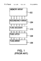
- FIG. 1 illustrates a typical dynamic random access memory (DRAM) integrated circuit, including a main memory array 202 .
- a redundant array 204 is provided as shown.
- a plurality of fuses in fuse array 206 are coupled to redundant array 204 via a fuse latch array 208 and a fuse decoder circuit 210 .
- individual fuses in fuse array 206 may be blown or cut to set their values to either a “1” or a “0” as required by the decoder circuit.
- the values of the fuses in fuse array 206 are typically loaded into fuse latch array 208 upon power up. These values are then decoded by fuse decoder circuit 210 during run time, thereby facilitating the replacement of specific failed main memory array elements with specific redundant elements of redundant array 204 . Techniques for replacing failed main memory array elements with redundant array elements are well known in the art and will not be discussed in great detail here for brevity's sake.
- the fuse links within fuse array 206 may be selectively blown or cut with a laser beam. Once blown by the laser beam, the fuse changes from a highly conductive state to a highly resistive, i.e., non-conductive state, i.e., a blown fuse inhibits current from flowing through and represents an open circuit to the current path.
- High density dynamic random access memories are designed with memory cell redundancy.
- the redundant memory cells are incorporated therein to prevent the loss of entire memories in the event that a minor number of memory cells do not function.
- Activation of the redundant memory cells is accomplished by fusible links which are strategically placed throughout the memory. Activation of a fusible link results in the disabling of the defective memory cell, while enabling in its place a redundant memory cell.
- the process of “blowing” fusible links is implemented by heating the fusible link which is to be blown.
- the heated fusible link melts or evaporates, creating an open circuit for replacing the defective memory cells with a functional cell.
- the fusible links are made of aluminum, copper and other high conductive metal or metal alloy.
- the conductive fusible link generally has a central width portion which is smaller than the ends to reduce the amount of energy necessary to melt the fusible link to create an open circuit condition.
- a small necked down portion of the fusible link acts as a fuse and can be blown out by an over-current or an over-voltage selectively applied in order to each memory cell.
- the fusible link is made of a thin film of refractory metal.
- FIG. 2 shows a schematic of a typical DRAM cell having a field effect transistor(FET) 100 and a fusible link 200 .
- the gate 110 of the FET 100 acts as the wordline W/L 120 .
- a bitline B/L 170 is connected to one terminal of the fusible link 200 .
- the other terminal of the fusible link 200 is connected to the one terminal 140 , e.g., a source terminal, of the FET 100 , depending on the applications such as read and write operations.
- the other DRAM terminal 150 e.g., a drain terminal, is referred to as a plate.
- the fusible link will melt causing an increase in volume when it is blown. Since, however, the melted fusible link was conventionally constrained within the a protective layer to prevent deterioration, it has to form a path by itself resulting in only a very small separation of the melted fusible link end. This can cause unwanted shorts or low resistance.
- FIG. 1 shows a typical DRAM integrated Circuit
- FIG. 2 shows an electrical schematic diagram for a conventional DRAM cell with a fusible link
- FIGS. 3 a to 3 c represent cross section views showing a fusible link at various stages of manufacture in accordance with the present invention.
- FIGS. 3 a to 3 c there is illustrated a method for forming a cavity for a fusible link on a silicon substrate in accordance with the present invention.
- Each of the fusible links is connected to circuitry on the silicon substrate for blowing redundant memory cells.
- the method is initiated with applying an etchable material over and around a portion of the fusible link. Specifically, first, a silicon substrate 20 is prepared and then a portion of the silicon substrate 20 is covered with an insulating layer 22 by a conventional depositing technique.
- the insulating layer 22 is made of an oxide such as a silicon oxide.
- a fusible line 28 is formed using conventional photolithographic methods.
- a film of gate material 24 such as a doped polysilicon and a gate wiring 26 such as a tungsten silicide WSi 2 are sequentially deposited over the silicon substrate 20 , and patterned lithographically and substantially etched to form the fusible line 28 including the doped polysilicon gate material 24 and tungsten silicide gate wiring 26 .
- the gate material 24 is formed of a polysilicon, which may be doped with either N + or P + impurities, and acts as the wordline W/L of the memory cell.
- the gate material 24 and the gate wiring 26 have a width that equals a minimum lithographic feature size.
- the fusible link is preferably connected to the gate region of the field effect transistor(FET), but it is noted that the fusible line may be connected to a source/drain region of the FET 10 .
- a nitride cover 30 is formed to cover the fusible line 28 , i.e., the gate wiring 26 and sidewalls of the gate material 24 .
- the entire top face of the nitride cover 30 is covered with a protective layer 32 of dielectric material.
- the protective layer 32 is made of a silicon oxide deposited at low temperature using chemical vapor deposition(CVD).
- the protective layer 32 is needed to protect the device from deterioration due to humidity and various surface effects. It is also used for isolation apart from the heat control layer.
- an access 36 through the protective layer 32 is formed by using a conventional lithography process. It is noted that the access 36 adjoins at least a portion of the nitride cover 30 . Specifically, a layer of photoresist mask 34 is applied, exposed and developed to form an etching hole 35 under which the access 36 is to exist. Then, the protective layer 32 is anisotropically etched to form the access 36 abutting the nitride cover 30 .
- the nitride cover 30 over and around the fusible line 28 is selectively removed by an isotropic etching, leaving the fusible link 28 surrounded by a cavity 38 . It is preferable that the nitride cover 30 is etched by a dry etching. Then, the mask is removed to expose the protective layer 32 as shown in FIG. 3 b.
- the access 36 is refilled with a refilling material 40 by a conventional depositing process.
- the refilling material 40 has a required viscosity so that almost all of the cavity 38 may remain without being refilled with the refilling material 40 as shown in FIG. 3 c .
- the cavity 38 may accommodate the molten metal of the fusible link 28 during the blowout thereof, thereby preventing unwanted shorts or low resistance therein.
Abstract
Description
Claims (6)
Priority Applications (3)
| Application Number | Priority Date | Filing Date | Title |
|---|---|---|---|
| US09/393,096 US6210995B1 (en) | 1999-09-09 | 1999-09-09 | Method for manufacturing fusible links in a semiconductor device |
| PCT/US2000/024402 WO2001018863A1 (en) | 1999-09-09 | 2000-09-06 | Method for manufacturing fusible links in a semiconductor device |
| TW089118329A TW499737B (en) | 1999-09-09 | 2000-09-07 | Method for manufacturing fusible links in a semiconductor device |
Applications Claiming Priority (1)
| Application Number | Priority Date | Filing Date | Title |
|---|---|---|---|
| US09/393,096 US6210995B1 (en) | 1999-09-09 | 1999-09-09 | Method for manufacturing fusible links in a semiconductor device |
Publications (1)
| Publication Number | Publication Date |
|---|---|
| US6210995B1 true US6210995B1 (en) | 2001-04-03 |
Family
ID=23553258
Family Applications (1)
| Application Number | Title | Priority Date | Filing Date |
|---|---|---|---|
| US09/393,096 Expired - Fee Related US6210995B1 (en) | 1999-09-09 | 1999-09-09 | Method for manufacturing fusible links in a semiconductor device |
Country Status (3)
| Country | Link |
|---|---|
| US (1) | US6210995B1 (en) |
| TW (1) | TW499737B (en) |
| WO (1) | WO2001018863A1 (en) |
Cited By (3)
| Publication number | Priority date | Publication date | Assignee | Title |
|---|---|---|---|---|
| US6480110B2 (en) * | 2000-12-01 | 2002-11-12 | Microchip Technology Incorporated | Inductively tunable antenna for a radio frequency identification tag |
| US20030119227A1 (en) * | 1999-11-10 | 2003-06-26 | Samsung Electronics Co. Ltd. | Architecture of laser fuse box of semiconductor integrated circuit and method for fabricating the same |
| US6828199B2 (en) * | 2001-12-20 | 2004-12-07 | Advanced Micro Devices, Ltd. | Monos device having buried metal silicide bit line |
Citations (11)
| Publication number | Priority date | Publication date | Assignee | Title |
|---|---|---|---|---|
| US4169000A (en) | 1976-09-02 | 1979-09-25 | International Business Machines Corporation | Method of forming an integrated circuit structure with fully-enclosed air isolation |
| US4209894A (en) | 1978-04-27 | 1980-07-01 | Texas Instruments Incorporated | Fusible-link semiconductor memory |
| US4460914A (en) | 1980-05-08 | 1984-07-17 | U.S. Philips Corporation | Programmable semiconductor device and method of manufacturing same |
| US4774561A (en) | 1985-05-23 | 1988-09-27 | Mitsubishi Denki Kabushiki Kaisha | Semiconductor device |
| US4879587A (en) | 1986-11-13 | 1989-11-07 | Transensory Devices, Inc. | Apparatus and method for forming fusible links |
| JPH034256A (en) | 1989-05-31 | 1991-01-10 | Toshiba Corp | Image forming device |
| JPH03169049A (en) | 1989-11-28 | 1991-07-22 | Nec Corp | Semiconductor integrated circuit |
| US5291434A (en) | 1989-07-13 | 1994-03-01 | Gemplus Card International | MOS fuse with oxide breakdown and application thereof to memory cards |
| US5585662A (en) | 1992-02-24 | 1996-12-17 | Nec Corporation | Semiconductor integrated circuit device with breakable fuse element covered with exactly controlled insulating film |
| US5641701A (en) | 1995-03-30 | 1997-06-24 | Texas Instruments Incorporated | Method for fabricating a semiconductor device with laser programable fuses |
| US5679967A (en) | 1985-01-20 | 1997-10-21 | Chip Express (Israel) Ltd. | Customizable three metal layer gate array devices |
Family Cites Families (4)
| Publication number | Priority date | Publication date | Assignee | Title |
|---|---|---|---|---|
| JPS5833865A (en) * | 1981-08-24 | 1983-02-28 | Toshiba Corp | Semiconductor memory device and manufacture thereof |
| JPS63307758A (en) * | 1987-06-09 | 1988-12-15 | Nec Corp | Integrated circuit device |
| DE19638666C1 (en) * | 1996-01-08 | 1997-11-20 | Siemens Ag | Fuse with a protective layer in an integrated semiconductor circuit and associated manufacturing process |
| US5899736A (en) * | 1997-09-19 | 1999-05-04 | Siemens Aktiengesellschaft | Techniques for forming electrically blowable fuses on an integrated circuit |
-
1999
- 1999-09-09 US US09/393,096 patent/US6210995B1/en not_active Expired - Fee Related
-
2000
- 2000-09-06 WO PCT/US2000/024402 patent/WO2001018863A1/en active Application Filing
- 2000-09-07 TW TW089118329A patent/TW499737B/en not_active IP Right Cessation
Patent Citations (12)
| Publication number | Priority date | Publication date | Assignee | Title |
|---|---|---|---|---|
| US4169000A (en) | 1976-09-02 | 1979-09-25 | International Business Machines Corporation | Method of forming an integrated circuit structure with fully-enclosed air isolation |
| US4209894A (en) | 1978-04-27 | 1980-07-01 | Texas Instruments Incorporated | Fusible-link semiconductor memory |
| US4460914A (en) | 1980-05-08 | 1984-07-17 | U.S. Philips Corporation | Programmable semiconductor device and method of manufacturing same |
| US4536948A (en) | 1980-05-08 | 1985-08-27 | U.S. Philips Corporation | Method of manufacturing programmable semiconductor device |
| US5679967A (en) | 1985-01-20 | 1997-10-21 | Chip Express (Israel) Ltd. | Customizable three metal layer gate array devices |
| US4774561A (en) | 1985-05-23 | 1988-09-27 | Mitsubishi Denki Kabushiki Kaisha | Semiconductor device |
| US4879587A (en) | 1986-11-13 | 1989-11-07 | Transensory Devices, Inc. | Apparatus and method for forming fusible links |
| JPH034256A (en) | 1989-05-31 | 1991-01-10 | Toshiba Corp | Image forming device |
| US5291434A (en) | 1989-07-13 | 1994-03-01 | Gemplus Card International | MOS fuse with oxide breakdown and application thereof to memory cards |
| JPH03169049A (en) | 1989-11-28 | 1991-07-22 | Nec Corp | Semiconductor integrated circuit |
| US5585662A (en) | 1992-02-24 | 1996-12-17 | Nec Corporation | Semiconductor integrated circuit device with breakable fuse element covered with exactly controlled insulating film |
| US5641701A (en) | 1995-03-30 | 1997-06-24 | Texas Instruments Incorporated | Method for fabricating a semiconductor device with laser programable fuses |
Cited By (4)
| Publication number | Priority date | Publication date | Assignee | Title |
|---|---|---|---|---|
| US20030119227A1 (en) * | 1999-11-10 | 2003-06-26 | Samsung Electronics Co. Ltd. | Architecture of laser fuse box of semiconductor integrated circuit and method for fabricating the same |
| US6682959B2 (en) * | 1999-11-10 | 2004-01-27 | Samsung Electronics Co., Ltd. | Architecture of laser fuse box of semiconductor integrated circuit and method for fabricating the same |
| US6480110B2 (en) * | 2000-12-01 | 2002-11-12 | Microchip Technology Incorporated | Inductively tunable antenna for a radio frequency identification tag |
| US6828199B2 (en) * | 2001-12-20 | 2004-12-07 | Advanced Micro Devices, Ltd. | Monos device having buried metal silicide bit line |
Also Published As
| Publication number | Publication date |
|---|---|
| WO2001018863A9 (en) | 2002-11-07 |
| TW499737B (en) | 2002-08-21 |
| WO2001018863A1 (en) | 2001-03-15 |
Similar Documents
| Publication | Publication Date | Title |
|---|---|---|
| US5324681A (en) | Method of making a 3-dimensional programmable antifuse for integrated circuits | |
| US6746947B2 (en) | Post-fuse blow corrosion prevention structure for copper fuses | |
| JP4263816B2 (en) | Semiconductor device and manufacturing method thereof | |
| US7288804B2 (en) | Electrically programmable π-shaped fuse structures and methods of fabrication thereof | |
| US6972220B2 (en) | Structures and methods of anti-fuse formation in SOI | |
| US8278155B2 (en) | Reprogrammable fuse structure and method | |
| KR100295061B1 (en) | Semiconductor device having chamfered silicide layer and method for manufacturing the same | |
| US5789795A (en) | Methods and apparatus for fabricationg anti-fuse devices | |
| US6335228B1 (en) | Method for making an anti-fuse | |
| US20060220174A1 (en) | E-Fuse and anti-E-Fuse device structures and methods | |
| US7425472B2 (en) | Semiconductor fuses and semiconductor devices containing the same | |
| US7745855B2 (en) | Single crystal fuse on air in bulk silicon | |
| US7784009B2 (en) | Electrically programmable π-shaped fuse structures and design process therefore | |
| US6210995B1 (en) | Method for manufacturing fusible links in a semiconductor device | |
| US7888255B2 (en) | Method of forming an antifuse and a conductive interconnect, and methods of forming DRAM circuitry | |
| US7026217B1 (en) | Method of forming an antifuse on a semiconductor substrate using wet oxidation of a nitrided substrate | |
| KR100192591B1 (en) | Method of manufacturing the repair circuit of semiconductor memory device | |
| US20070190751A1 (en) | Semiconductor fuses and methods for fabricating and programming the same | |
| KR100334388B1 (en) | Manufacturing method for antifuse of semiconductor device | |
| JPH1126589A (en) | Manufacture of semiconductor device | |
| JPH10289955A (en) | Manufacture of semiconductor device | |
| KR20010061008A (en) | Manufacturing method for anti-fuse of semiconductor device | |
| JPH08340049A (en) | Integrated circuit correction method |
Legal Events
| Date | Code | Title | Description |
|---|---|---|---|
| AS | Assignment |
Owner name: INTERNATIONAL BUSINESS MACHINES CORPORATION, NEW Y Free format text: ASSIGNMENT OF ASSIGNORS INTEREST;ASSIGNORS:GAMBINO, JEFFREY;HALLE, SCOTT;REEL/FRAME:010240/0974;SIGNING DATES FROM 19990819 TO 19990903 Owner name: INFINEON TECHNOLOGIES CORPORATION, CALIFORNIA Free format text: ASSIGNMENT OF ASSIGNORS INTEREST;ASSIGNORS:BRINTZINGER, AXEL C.;RUPP, THOMAS;REEL/FRAME:010235/0262;SIGNING DATES FROM 19990816 TO 19990909 |
|
| AS | Assignment |
Owner name: INFINEON TECHNOLOGIES NORTH AMERICA CORP., CALIFOR Free format text: CHANGE OF NAME;ASSIGNOR:INFINEON TECHNOLOGIES CORPORATION;REEL/FRAME:010884/0487 Effective date: 19990930 |
|
| FEPP | Fee payment procedure |
Free format text: PAYOR NUMBER ASSIGNED (ORIGINAL EVENT CODE: ASPN); ENTITY STATUS OF PATENT OWNER: LARGE ENTITY |
|
| FPAY | Fee payment |
Year of fee payment: 4 |
|
| REMI | Maintenance fee reminder mailed | ||
| LAPS | Lapse for failure to pay maintenance fees | ||
| STCH | Information on status: patent discontinuation |
Free format text: PATENT EXPIRED DUE TO NONPAYMENT OF MAINTENANCE FEES UNDER 37 CFR 1.362 |
|
| FP | Lapsed due to failure to pay maintenance fee |
Effective date: 20090403 |