US6175157B1 - Semiconductor device package for suppressing warping in semiconductor chips - Google Patents
Semiconductor device package for suppressing warping in semiconductor chips Download PDFInfo
- Publication number
- US6175157B1 US6175157B1 US09/045,135 US4513598A US6175157B1 US 6175157 B1 US6175157 B1 US 6175157B1 US 4513598 A US4513598 A US 4513598A US 6175157 B1 US6175157 B1 US 6175157B1
- Authority
- US
- United States
- Prior art keywords
- bumps
- connecting surface
- semiconductor chip
- chip
- semiconductor device
- Prior art date
- Legal status (The legal status is an assumption and is not a legal conclusion. Google has not performed a legal analysis and makes no representation as to the accuracy of the status listed.)
- Expired - Lifetime
Links
- 239000004065 semiconductor Substances 0.000 title claims abstract description 66
- 238000000034 method Methods 0.000 claims description 6
- 125000006850 spacer group Chemical group 0.000 claims description 4
- 239000004840 adhesive resin Substances 0.000 claims description 3
- 229920006223 adhesive resin Polymers 0.000 claims description 3
- 239000002245 particle Substances 0.000 claims description 3
- 239000011347 resin Substances 0.000 abstract 1
- 229920005989 resin Polymers 0.000 abstract 1
- 239000000463 material Substances 0.000 description 4
- 239000010931 gold Substances 0.000 description 3
- 239000004020 conductor Substances 0.000 description 2
- PCHJSUWPFVWCPO-UHFFFAOYSA-N gold Chemical compound [Au] PCHJSUWPFVWCPO-UHFFFAOYSA-N 0.000 description 2
- 229910052737 gold Inorganic materials 0.000 description 2
- 239000002184 metal Substances 0.000 description 2
- 229910052751 metal Inorganic materials 0.000 description 2
- 229910000679 solder Inorganic materials 0.000 description 2
- 229920003002 synthetic resin Polymers 0.000 description 2
- 239000000057 synthetic resin Substances 0.000 description 2
- 229910020220 Pb—Sn Inorganic materials 0.000 description 1
- 238000001704 evaporation Methods 0.000 description 1
- 230000001747 exhibiting effect Effects 0.000 description 1
- 239000011810 insulating material Substances 0.000 description 1
- 230000010354 integration Effects 0.000 description 1
- 230000004048 modification Effects 0.000 description 1
- 238000012986 modification Methods 0.000 description 1
- 238000007747 plating Methods 0.000 description 1
- 238000001721 transfer moulding Methods 0.000 description 1
Images


Classifications
-
- H—ELECTRICITY
- H01—ELECTRIC ELEMENTS
- H01L—SEMICONDUCTOR DEVICES NOT COVERED BY CLASS H10
- H01L24/00—Arrangements for connecting or disconnecting semiconductor or solid-state bodies; Methods or apparatus related thereto
- H01L24/80—Methods for connecting semiconductor or other solid state bodies using means for bonding being attached to, or being formed on, the surface to be connected
- H01L24/83—Methods for connecting semiconductor or other solid state bodies using means for bonding being attached to, or being formed on, the surface to be connected using a layer connector
-
- H—ELECTRICITY
- H01—ELECTRIC ELEMENTS
- H01L—SEMICONDUCTOR DEVICES NOT COVERED BY CLASS H10
- H01L21/00—Processes or apparatus adapted for the manufacture or treatment of semiconductor or solid state devices or of parts thereof
- H01L21/02—Manufacture or treatment of semiconductor devices or of parts thereof
- H01L21/04—Manufacture or treatment of semiconductor devices or of parts thereof the devices having at least one potential-jump barrier or surface barrier, e.g. PN junction, depletion layer or carrier concentration layer
- H01L21/50—Assembly of semiconductor devices using processes or apparatus not provided for in a single one of the subgroups H01L21/06 - H01L21/326, e.g. sealing of a cap to a base of a container
- H01L21/56—Encapsulations, e.g. encapsulation layers, coatings
- H01L21/563—Encapsulation of active face of flip-chip device, e.g. underfilling or underencapsulation of flip-chip, encapsulation preform on chip or mounting substrate
-
- H—ELECTRICITY
- H01—ELECTRIC ELEMENTS
- H01L—SEMICONDUCTOR DEVICES NOT COVERED BY CLASS H10
- H01L23/00—Details of semiconductor or other solid state devices
- H01L23/48—Arrangements for conducting electric current to or from the solid state body in operation, e.g. leads, terminal arrangements ; Selection of materials therefor
- H01L23/488—Arrangements for conducting electric current to or from the solid state body in operation, e.g. leads, terminal arrangements ; Selection of materials therefor consisting of soldered or bonded constructions
- H01L23/495—Lead-frames or other flat leads
- H01L23/49575—Assemblies of semiconductor devices on lead frames
-
- H—ELECTRICITY
- H01—ELECTRIC ELEMENTS
- H01L—SEMICONDUCTOR DEVICES NOT COVERED BY CLASS H10
- H01L24/00—Arrangements for connecting or disconnecting semiconductor or solid-state bodies; Methods or apparatus related thereto
- H01L24/01—Means for bonding being attached to, or being formed on, the surface to be connected, e.g. chip-to-package, die-attach, "first-level" interconnects; Manufacturing methods related thereto
- H01L24/26—Layer connectors, e.g. plate connectors, solder or adhesive layers; Manufacturing methods related thereto
- H01L24/28—Structure, shape, material or disposition of the layer connectors prior to the connecting process
- H01L24/29—Structure, shape, material or disposition of the layer connectors prior to the connecting process of an individual layer connector
-
- H—ELECTRICITY
- H01—ELECTRIC ELEMENTS
- H01L—SEMICONDUCTOR DEVICES NOT COVERED BY CLASS H10
- H01L24/00—Arrangements for connecting or disconnecting semiconductor or solid-state bodies; Methods or apparatus related thereto
- H01L24/80—Methods for connecting semiconductor or other solid state bodies using means for bonding being attached to, or being formed on, the surface to be connected
- H01L24/81—Methods for connecting semiconductor or other solid state bodies using means for bonding being attached to, or being formed on, the surface to be connected using a bump connector
-
- H—ELECTRICITY
- H01—ELECTRIC ELEMENTS
- H01L—SEMICONDUCTOR DEVICES NOT COVERED BY CLASS H10
- H01L25/00—Assemblies consisting of a plurality of individual semiconductor or other solid state devices ; Multistep manufacturing processes thereof
- H01L25/03—Assemblies consisting of a plurality of individual semiconductor or other solid state devices ; Multistep manufacturing processes thereof all the devices being of a type provided for in the same subgroup of groups H01L27/00 - H01L33/00, or in a single subclass of H10K, H10N, e.g. assemblies of rectifier diodes
- H01L25/04—Assemblies consisting of a plurality of individual semiconductor or other solid state devices ; Multistep manufacturing processes thereof all the devices being of a type provided for in the same subgroup of groups H01L27/00 - H01L33/00, or in a single subclass of H10K, H10N, e.g. assemblies of rectifier diodes the devices not having separate containers
- H01L25/065—Assemblies consisting of a plurality of individual semiconductor or other solid state devices ; Multistep manufacturing processes thereof all the devices being of a type provided for in the same subgroup of groups H01L27/00 - H01L33/00, or in a single subclass of H10K, H10N, e.g. assemblies of rectifier diodes the devices not having separate containers the devices being of a type provided for in group H01L27/00
- H01L25/0657—Stacked arrangements of devices
-
- H—ELECTRICITY
- H01—ELECTRIC ELEMENTS
- H01L—SEMICONDUCTOR DEVICES NOT COVERED BY CLASS H10
- H01L2224/00—Indexing scheme for arrangements for connecting or disconnecting semiconductor or solid-state bodies and methods related thereto as covered by H01L24/00
- H01L2224/01—Means for bonding being attached to, or being formed on, the surface to be connected, e.g. chip-to-package, die-attach, "first-level" interconnects; Manufacturing methods related thereto
- H01L2224/02—Bonding areas; Manufacturing methods related thereto
- H01L2224/04—Structure, shape, material or disposition of the bonding areas prior to the connecting process
- H01L2224/05—Structure, shape, material or disposition of the bonding areas prior to the connecting process of an individual bonding area
- H01L2224/0554—External layer
- H01L2224/0555—Shape
- H01L2224/05552—Shape in top view
- H01L2224/05553—Shape in top view being rectangular
-
- H—ELECTRICITY
- H01—ELECTRIC ELEMENTS
- H01L—SEMICONDUCTOR DEVICES NOT COVERED BY CLASS H10
- H01L2224/00—Indexing scheme for arrangements for connecting or disconnecting semiconductor or solid-state bodies and methods related thereto as covered by H01L24/00
- H01L2224/01—Means for bonding being attached to, or being formed on, the surface to be connected, e.g. chip-to-package, die-attach, "first-level" interconnects; Manufacturing methods related thereto
- H01L2224/02—Bonding areas; Manufacturing methods related thereto
- H01L2224/04—Structure, shape, material or disposition of the bonding areas prior to the connecting process
- H01L2224/05—Structure, shape, material or disposition of the bonding areas prior to the connecting process of an individual bonding area
- H01L2224/0554—External layer
- H01L2224/0556—Disposition
- H01L2224/05568—Disposition the whole external layer protruding from the surface
-
- H—ELECTRICITY
- H01—ELECTRIC ELEMENTS
- H01L—SEMICONDUCTOR DEVICES NOT COVERED BY CLASS H10
- H01L2224/00—Indexing scheme for arrangements for connecting or disconnecting semiconductor or solid-state bodies and methods related thereto as covered by H01L24/00
- H01L2224/01—Means for bonding being attached to, or being formed on, the surface to be connected, e.g. chip-to-package, die-attach, "first-level" interconnects; Manufacturing methods related thereto
- H01L2224/02—Bonding areas; Manufacturing methods related thereto
- H01L2224/04—Structure, shape, material or disposition of the bonding areas prior to the connecting process
- H01L2224/05—Structure, shape, material or disposition of the bonding areas prior to the connecting process of an individual bonding area
- H01L2224/0554—External layer
- H01L2224/05573—Single external layer
-
- H—ELECTRICITY
- H01—ELECTRIC ELEMENTS
- H01L—SEMICONDUCTOR DEVICES NOT COVERED BY CLASS H10
- H01L2224/00—Indexing scheme for arrangements for connecting or disconnecting semiconductor or solid-state bodies and methods related thereto as covered by H01L24/00
- H01L2224/01—Means for bonding being attached to, or being formed on, the surface to be connected, e.g. chip-to-package, die-attach, "first-level" interconnects; Manufacturing methods related thereto
- H01L2224/10—Bump connectors; Manufacturing methods related thereto
- H01L2224/12—Structure, shape, material or disposition of the bump connectors prior to the connecting process
- H01L2224/13—Structure, shape, material or disposition of the bump connectors prior to the connecting process of an individual bump connector
- H01L2224/13001—Core members of the bump connector
- H01L2224/13099—Material
- H01L2224/131—Material with a principal constituent of the material being a metal or a metalloid, e.g. boron [B], silicon [Si], germanium [Ge], arsenic [As], antimony [Sb], tellurium [Te] and polonium [Po], and alloys thereof
- H01L2224/13101—Material with a principal constituent of the material being a metal or a metalloid, e.g. boron [B], silicon [Si], germanium [Ge], arsenic [As], antimony [Sb], tellurium [Te] and polonium [Po], and alloys thereof the principal constituent melting at a temperature of less than 400°C
- H01L2224/13111—Tin [Sn] as principal constituent
-
- H—ELECTRICITY
- H01—ELECTRIC ELEMENTS
- H01L—SEMICONDUCTOR DEVICES NOT COVERED BY CLASS H10
- H01L2224/00—Indexing scheme for arrangements for connecting or disconnecting semiconductor or solid-state bodies and methods related thereto as covered by H01L24/00
- H01L2224/01—Means for bonding being attached to, or being formed on, the surface to be connected, e.g. chip-to-package, die-attach, "first-level" interconnects; Manufacturing methods related thereto
- H01L2224/10—Bump connectors; Manufacturing methods related thereto
- H01L2224/12—Structure, shape, material or disposition of the bump connectors prior to the connecting process
- H01L2224/13—Structure, shape, material or disposition of the bump connectors prior to the connecting process of an individual bump connector
- H01L2224/13001—Core members of the bump connector
- H01L2224/13099—Material
- H01L2224/131—Material with a principal constituent of the material being a metal or a metalloid, e.g. boron [B], silicon [Si], germanium [Ge], arsenic [As], antimony [Sb], tellurium [Te] and polonium [Po], and alloys thereof
- H01L2224/13138—Material with a principal constituent of the material being a metal or a metalloid, e.g. boron [B], silicon [Si], germanium [Ge], arsenic [As], antimony [Sb], tellurium [Te] and polonium [Po], and alloys thereof the principal constituent melting at a temperature of greater than or equal to 950°C and less than 1550°C
- H01L2224/13144—Gold [Au] as principal constituent
-
- H—ELECTRICITY
- H01—ELECTRIC ELEMENTS
- H01L—SEMICONDUCTOR DEVICES NOT COVERED BY CLASS H10
- H01L2224/00—Indexing scheme for arrangements for connecting or disconnecting semiconductor or solid-state bodies and methods related thereto as covered by H01L24/00
- H01L2224/01—Means for bonding being attached to, or being formed on, the surface to be connected, e.g. chip-to-package, die-attach, "first-level" interconnects; Manufacturing methods related thereto
- H01L2224/10—Bump connectors; Manufacturing methods related thereto
- H01L2224/15—Structure, shape, material or disposition of the bump connectors after the connecting process
- H01L2224/16—Structure, shape, material or disposition of the bump connectors after the connecting process of an individual bump connector
- H01L2224/161—Disposition
- H01L2224/16135—Disposition the bump connector connecting between different semiconductor or solid-state bodies, i.e. chip-to-chip
- H01L2224/16145—Disposition the bump connector connecting between different semiconductor or solid-state bodies, i.e. chip-to-chip the bodies being stacked
-
- H—ELECTRICITY
- H01—ELECTRIC ELEMENTS
- H01L—SEMICONDUCTOR DEVICES NOT COVERED BY CLASS H10
- H01L2224/00—Indexing scheme for arrangements for connecting or disconnecting semiconductor or solid-state bodies and methods related thereto as covered by H01L24/00
- H01L2224/01—Means for bonding being attached to, or being formed on, the surface to be connected, e.g. chip-to-package, die-attach, "first-level" interconnects; Manufacturing methods related thereto
- H01L2224/26—Layer connectors, e.g. plate connectors, solder or adhesive layers; Manufacturing methods related thereto
- H01L2224/28—Structure, shape, material or disposition of the layer connectors prior to the connecting process
- H01L2224/29—Structure, shape, material or disposition of the layer connectors prior to the connecting process of an individual layer connector
- H01L2224/29001—Core members of the layer connector
- H01L2224/29099—Material
- H01L2224/291—Material with a principal constituent of the material being a metal or a metalloid, e.g. boron [B], silicon [Si], germanium [Ge], arsenic [As], antimony [Sb], tellurium [Te] and polonium [Po], and alloys thereof
- H01L2224/29101—Material with a principal constituent of the material being a metal or a metalloid, e.g. boron [B], silicon [Si], germanium [Ge], arsenic [As], antimony [Sb], tellurium [Te] and polonium [Po], and alloys thereof the principal constituent melting at a temperature of less than 400°C
- H01L2224/29111—Tin [Sn] as principal constituent
-
- H—ELECTRICITY
- H01—ELECTRIC ELEMENTS
- H01L—SEMICONDUCTOR DEVICES NOT COVERED BY CLASS H10
- H01L2224/00—Indexing scheme for arrangements for connecting or disconnecting semiconductor or solid-state bodies and methods related thereto as covered by H01L24/00
- H01L2224/01—Means for bonding being attached to, or being formed on, the surface to be connected, e.g. chip-to-package, die-attach, "first-level" interconnects; Manufacturing methods related thereto
- H01L2224/26—Layer connectors, e.g. plate connectors, solder or adhesive layers; Manufacturing methods related thereto
- H01L2224/28—Structure, shape, material or disposition of the layer connectors prior to the connecting process
- H01L2224/29—Structure, shape, material or disposition of the layer connectors prior to the connecting process of an individual layer connector
- H01L2224/29001—Core members of the layer connector
- H01L2224/29099—Material
- H01L2224/29198—Material with a principal constituent of the material being a combination of two or more materials in the form of a matrix with a filler, i.e. being a hybrid material, e.g. segmented structures, foams
- H01L2224/29199—Material of the matrix
- H01L2224/2929—Material of the matrix with a principal constituent of the material being a polymer, e.g. polyester, phenolic based polymer, epoxy
-
- H—ELECTRICITY
- H01—ELECTRIC ELEMENTS
- H01L—SEMICONDUCTOR DEVICES NOT COVERED BY CLASS H10
- H01L2224/00—Indexing scheme for arrangements for connecting or disconnecting semiconductor or solid-state bodies and methods related thereto as covered by H01L24/00
- H01L2224/01—Means for bonding being attached to, or being formed on, the surface to be connected, e.g. chip-to-package, die-attach, "first-level" interconnects; Manufacturing methods related thereto
- H01L2224/26—Layer connectors, e.g. plate connectors, solder or adhesive layers; Manufacturing methods related thereto
- H01L2224/28—Structure, shape, material or disposition of the layer connectors prior to the connecting process
- H01L2224/29—Structure, shape, material or disposition of the layer connectors prior to the connecting process of an individual layer connector
- H01L2224/29001—Core members of the layer connector
- H01L2224/29099—Material
- H01L2224/29198—Material with a principal constituent of the material being a combination of two or more materials in the form of a matrix with a filler, i.e. being a hybrid material, e.g. segmented structures, foams
- H01L2224/29298—Fillers
- H01L2224/29299—Base material
-
- H—ELECTRICITY
- H01—ELECTRIC ELEMENTS
- H01L—SEMICONDUCTOR DEVICES NOT COVERED BY CLASS H10
- H01L2224/00—Indexing scheme for arrangements for connecting or disconnecting semiconductor or solid-state bodies and methods related thereto as covered by H01L24/00
- H01L2224/01—Means for bonding being attached to, or being formed on, the surface to be connected, e.g. chip-to-package, die-attach, "first-level" interconnects; Manufacturing methods related thereto
- H01L2224/26—Layer connectors, e.g. plate connectors, solder or adhesive layers; Manufacturing methods related thereto
- H01L2224/31—Structure, shape, material or disposition of the layer connectors after the connecting process
- H01L2224/32—Structure, shape, material or disposition of the layer connectors after the connecting process of an individual layer connector
- H01L2224/321—Disposition
- H01L2224/32135—Disposition the layer connector connecting between different semiconductor or solid-state bodies, i.e. chip-to-chip
- H01L2224/32145—Disposition the layer connector connecting between different semiconductor or solid-state bodies, i.e. chip-to-chip the bodies being stacked
-
- H—ELECTRICITY
- H01—ELECTRIC ELEMENTS
- H01L—SEMICONDUCTOR DEVICES NOT COVERED BY CLASS H10
- H01L2224/00—Indexing scheme for arrangements for connecting or disconnecting semiconductor or solid-state bodies and methods related thereto as covered by H01L24/00
- H01L2224/01—Means for bonding being attached to, or being formed on, the surface to be connected, e.g. chip-to-package, die-attach, "first-level" interconnects; Manufacturing methods related thereto
- H01L2224/42—Wire connectors; Manufacturing methods related thereto
- H01L2224/44—Structure, shape, material or disposition of the wire connectors prior to the connecting process
- H01L2224/45—Structure, shape, material or disposition of the wire connectors prior to the connecting process of an individual wire connector
- H01L2224/45001—Core members of the connector
- H01L2224/45099—Material
- H01L2224/451—Material with a principal constituent of the material being a metal or a metalloid, e.g. boron (B), silicon (Si), germanium (Ge), arsenic (As), antimony (Sb), tellurium (Te) and polonium (Po), and alloys thereof
-
- H—ELECTRICITY
- H01—ELECTRIC ELEMENTS
- H01L—SEMICONDUCTOR DEVICES NOT COVERED BY CLASS H10
- H01L2224/00—Indexing scheme for arrangements for connecting or disconnecting semiconductor or solid-state bodies and methods related thereto as covered by H01L24/00
- H01L2224/01—Means for bonding being attached to, or being formed on, the surface to be connected, e.g. chip-to-package, die-attach, "first-level" interconnects; Manufacturing methods related thereto
- H01L2224/42—Wire connectors; Manufacturing methods related thereto
- H01L2224/47—Structure, shape, material or disposition of the wire connectors after the connecting process
- H01L2224/48—Structure, shape, material or disposition of the wire connectors after the connecting process of an individual wire connector
- H01L2224/4805—Shape
- H01L2224/4809—Loop shape
- H01L2224/48091—Arched
-
- H—ELECTRICITY
- H01—ELECTRIC ELEMENTS
- H01L—SEMICONDUCTOR DEVICES NOT COVERED BY CLASS H10
- H01L2224/00—Indexing scheme for arrangements for connecting or disconnecting semiconductor or solid-state bodies and methods related thereto as covered by H01L24/00
- H01L2224/01—Means for bonding being attached to, or being formed on, the surface to be connected, e.g. chip-to-package, die-attach, "first-level" interconnects; Manufacturing methods related thereto
- H01L2224/42—Wire connectors; Manufacturing methods related thereto
- H01L2224/47—Structure, shape, material or disposition of the wire connectors after the connecting process
- H01L2224/48—Structure, shape, material or disposition of the wire connectors after the connecting process of an individual wire connector
- H01L2224/481—Disposition
- H01L2224/48151—Connecting between a semiconductor or solid-state body and an item not being a semiconductor or solid-state body, e.g. chip-to-substrate, chip-to-passive
- H01L2224/48221—Connecting between a semiconductor or solid-state body and an item not being a semiconductor or solid-state body, e.g. chip-to-substrate, chip-to-passive the body and the item being stacked
- H01L2224/48245—Connecting between a semiconductor or solid-state body and an item not being a semiconductor or solid-state body, e.g. chip-to-substrate, chip-to-passive the body and the item being stacked the item being metallic
- H01L2224/48247—Connecting between a semiconductor or solid-state body and an item not being a semiconductor or solid-state body, e.g. chip-to-substrate, chip-to-passive the body and the item being stacked the item being metallic connecting the wire to a bond pad of the item
-
- H—ELECTRICITY
- H01—ELECTRIC ELEMENTS
- H01L—SEMICONDUCTOR DEVICES NOT COVERED BY CLASS H10
- H01L2224/00—Indexing scheme for arrangements for connecting or disconnecting semiconductor or solid-state bodies and methods related thereto as covered by H01L24/00
- H01L2224/73—Means for bonding being of different types provided for in two or more of groups H01L2224/10, H01L2224/18, H01L2224/26, H01L2224/34, H01L2224/42, H01L2224/50, H01L2224/63, H01L2224/71
- H01L2224/732—Location after the connecting process
- H01L2224/73201—Location after the connecting process on the same surface
- H01L2224/73203—Bump and layer connectors
- H01L2224/73204—Bump and layer connectors the bump connector being embedded into the layer connector
-
- H—ELECTRICITY
- H01—ELECTRIC ELEMENTS
- H01L—SEMICONDUCTOR DEVICES NOT COVERED BY CLASS H10
- H01L2224/00—Indexing scheme for arrangements for connecting or disconnecting semiconductor or solid-state bodies and methods related thereto as covered by H01L24/00
- H01L2224/80—Methods for connecting semiconductor or other solid state bodies using means for bonding being attached to, or being formed on, the surface to be connected
- H01L2224/81—Methods for connecting semiconductor or other solid state bodies using means for bonding being attached to, or being formed on, the surface to be connected using a bump connector
- H01L2224/818—Bonding techniques
- H01L2224/81801—Soldering or alloying
-
- H—ELECTRICITY
- H01—ELECTRIC ELEMENTS
- H01L—SEMICONDUCTOR DEVICES NOT COVERED BY CLASS H10
- H01L2224/00—Indexing scheme for arrangements for connecting or disconnecting semiconductor or solid-state bodies and methods related thereto as covered by H01L24/00
- H01L2224/80—Methods for connecting semiconductor or other solid state bodies using means for bonding being attached to, or being formed on, the surface to be connected
- H01L2224/83—Methods for connecting semiconductor or other solid state bodies using means for bonding being attached to, or being formed on, the surface to be connected using a layer connector
- H01L2224/831—Methods for connecting semiconductor or other solid state bodies using means for bonding being attached to, or being formed on, the surface to be connected using a layer connector the layer connector being supplied to the parts to be connected in the bonding apparatus
- H01L2224/83101—Methods for connecting semiconductor or other solid state bodies using means for bonding being attached to, or being formed on, the surface to be connected using a layer connector the layer connector being supplied to the parts to be connected in the bonding apparatus as prepeg comprising a layer connector, e.g. provided in an insulating plate member
-
- H—ELECTRICITY
- H01—ELECTRIC ELEMENTS
- H01L—SEMICONDUCTOR DEVICES NOT COVERED BY CLASS H10
- H01L2224/00—Indexing scheme for arrangements for connecting or disconnecting semiconductor or solid-state bodies and methods related thereto as covered by H01L24/00
- H01L2224/80—Methods for connecting semiconductor or other solid state bodies using means for bonding being attached to, or being formed on, the surface to be connected
- H01L2224/83—Methods for connecting semiconductor or other solid state bodies using means for bonding being attached to, or being formed on, the surface to be connected using a layer connector
- H01L2224/8319—Arrangement of the layer connectors prior to mounting
-
- H—ELECTRICITY
- H01—ELECTRIC ELEMENTS
- H01L—SEMICONDUCTOR DEVICES NOT COVERED BY CLASS H10
- H01L2224/00—Indexing scheme for arrangements for connecting or disconnecting semiconductor or solid-state bodies and methods related thereto as covered by H01L24/00
- H01L2224/80—Methods for connecting semiconductor or other solid state bodies using means for bonding being attached to, or being formed on, the surface to be connected
- H01L2224/83—Methods for connecting semiconductor or other solid state bodies using means for bonding being attached to, or being formed on, the surface to be connected using a layer connector
- H01L2224/838—Bonding techniques
-
- H—ELECTRICITY
- H01—ELECTRIC ELEMENTS
- H01L—SEMICONDUCTOR DEVICES NOT COVERED BY CLASS H10
- H01L2225/00—Details relating to assemblies covered by the group H01L25/00 but not provided for in its subgroups
- H01L2225/03—All the devices being of a type provided for in the same subgroup of groups H01L27/00 - H01L33/648 and H10K99/00
- H01L2225/04—All the devices being of a type provided for in the same subgroup of groups H01L27/00 - H01L33/648 and H10K99/00 the devices not having separate containers
- H01L2225/065—All the devices being of a type provided for in the same subgroup of groups H01L27/00 - H01L33/648 and H10K99/00 the devices not having separate containers the devices being of a type provided for in group H01L27/00
- H01L2225/06503—Stacked arrangements of devices
- H01L2225/0651—Wire or wire-like electrical connections from device to substrate
-
- H—ELECTRICITY
- H01—ELECTRIC ELEMENTS
- H01L—SEMICONDUCTOR DEVICES NOT COVERED BY CLASS H10
- H01L2225/00—Details relating to assemblies covered by the group H01L25/00 but not provided for in its subgroups
- H01L2225/03—All the devices being of a type provided for in the same subgroup of groups H01L27/00 - H01L33/648 and H10K99/00
- H01L2225/04—All the devices being of a type provided for in the same subgroup of groups H01L27/00 - H01L33/648 and H10K99/00 the devices not having separate containers
- H01L2225/065—All the devices being of a type provided for in the same subgroup of groups H01L27/00 - H01L33/648 and H10K99/00 the devices not having separate containers the devices being of a type provided for in group H01L27/00
- H01L2225/06503—Stacked arrangements of devices
- H01L2225/06513—Bump or bump-like direct electrical connections between devices, e.g. flip-chip connection, solder bumps
-
- H—ELECTRICITY
- H01—ELECTRIC ELEMENTS
- H01L—SEMICONDUCTOR DEVICES NOT COVERED BY CLASS H10
- H01L2225/00—Details relating to assemblies covered by the group H01L25/00 but not provided for in its subgroups
- H01L2225/03—All the devices being of a type provided for in the same subgroup of groups H01L27/00 - H01L33/648 and H10K99/00
- H01L2225/04—All the devices being of a type provided for in the same subgroup of groups H01L27/00 - H01L33/648 and H10K99/00 the devices not having separate containers
- H01L2225/065—All the devices being of a type provided for in the same subgroup of groups H01L27/00 - H01L33/648 and H10K99/00 the devices not having separate containers the devices being of a type provided for in group H01L27/00
- H01L2225/06503—Stacked arrangements of devices
- H01L2225/06582—Housing for the assembly, e.g. chip scale package [CSP]
-
- H—ELECTRICITY
- H01—ELECTRIC ELEMENTS
- H01L—SEMICONDUCTOR DEVICES NOT COVERED BY CLASS H10
- H01L24/00—Arrangements for connecting or disconnecting semiconductor or solid-state bodies; Methods or apparatus related thereto
- H01L24/01—Means for bonding being attached to, or being formed on, the surface to be connected, e.g. chip-to-package, die-attach, "first-level" interconnects; Manufacturing methods related thereto
- H01L24/02—Bonding areas ; Manufacturing methods related thereto
- H01L24/04—Structure, shape, material or disposition of the bonding areas prior to the connecting process
- H01L24/05—Structure, shape, material or disposition of the bonding areas prior to the connecting process of an individual bonding area
-
- H—ELECTRICITY
- H01—ELECTRIC ELEMENTS
- H01L—SEMICONDUCTOR DEVICES NOT COVERED BY CLASS H10
- H01L24/00—Arrangements for connecting or disconnecting semiconductor or solid-state bodies; Methods or apparatus related thereto
- H01L24/01—Means for bonding being attached to, or being formed on, the surface to be connected, e.g. chip-to-package, die-attach, "first-level" interconnects; Manufacturing methods related thereto
- H01L24/42—Wire connectors; Manufacturing methods related thereto
- H01L24/44—Structure, shape, material or disposition of the wire connectors prior to the connecting process
- H01L24/45—Structure, shape, material or disposition of the wire connectors prior to the connecting process of an individual wire connector
-
- H—ELECTRICITY
- H01—ELECTRIC ELEMENTS
- H01L—SEMICONDUCTOR DEVICES NOT COVERED BY CLASS H10
- H01L24/00—Arrangements for connecting or disconnecting semiconductor or solid-state bodies; Methods or apparatus related thereto
- H01L24/01—Means for bonding being attached to, or being formed on, the surface to be connected, e.g. chip-to-package, die-attach, "first-level" interconnects; Manufacturing methods related thereto
- H01L24/42—Wire connectors; Manufacturing methods related thereto
- H01L24/47—Structure, shape, material or disposition of the wire connectors after the connecting process
- H01L24/48—Structure, shape, material or disposition of the wire connectors after the connecting process of an individual wire connector
-
- H—ELECTRICITY
- H01—ELECTRIC ELEMENTS
- H01L—SEMICONDUCTOR DEVICES NOT COVERED BY CLASS H10
- H01L2924/00—Indexing scheme for arrangements or methods for connecting or disconnecting semiconductor or solid-state bodies as covered by H01L24/00
- H01L2924/0001—Technical content checked by a classifier
- H01L2924/00013—Fully indexed content
-
- H—ELECTRICITY
- H01—ELECTRIC ELEMENTS
- H01L—SEMICONDUCTOR DEVICES NOT COVERED BY CLASS H10
- H01L2924/00—Indexing scheme for arrangements or methods for connecting or disconnecting semiconductor or solid-state bodies as covered by H01L24/00
- H01L2924/0001—Technical content checked by a classifier
- H01L2924/00014—Technical content checked by a classifier the subject-matter covered by the group, the symbol of which is combined with the symbol of this group, being disclosed without further technical details
-
- H—ELECTRICITY
- H01—ELECTRIC ELEMENTS
- H01L—SEMICONDUCTOR DEVICES NOT COVERED BY CLASS H10
- H01L2924/00—Indexing scheme for arrangements or methods for connecting or disconnecting semiconductor or solid-state bodies as covered by H01L24/00
- H01L2924/01—Chemical elements
- H01L2924/01033—Arsenic [As]
-
- H—ELECTRICITY
- H01—ELECTRIC ELEMENTS
- H01L—SEMICONDUCTOR DEVICES NOT COVERED BY CLASS H10
- H01L2924/00—Indexing scheme for arrangements or methods for connecting or disconnecting semiconductor or solid-state bodies as covered by H01L24/00
- H01L2924/01—Chemical elements
- H01L2924/0105—Tin [Sn]
-
- H—ELECTRICITY
- H01—ELECTRIC ELEMENTS
- H01L—SEMICONDUCTOR DEVICES NOT COVERED BY CLASS H10
- H01L2924/00—Indexing scheme for arrangements or methods for connecting or disconnecting semiconductor or solid-state bodies as covered by H01L24/00
- H01L2924/01—Chemical elements
- H01L2924/01078—Platinum [Pt]
-
- H—ELECTRICITY
- H01—ELECTRIC ELEMENTS
- H01L—SEMICONDUCTOR DEVICES NOT COVERED BY CLASS H10
- H01L2924/00—Indexing scheme for arrangements or methods for connecting or disconnecting semiconductor or solid-state bodies as covered by H01L24/00
- H01L2924/01—Chemical elements
- H01L2924/01079—Gold [Au]
-
- H—ELECTRICITY
- H01—ELECTRIC ELEMENTS
- H01L—SEMICONDUCTOR DEVICES NOT COVERED BY CLASS H10
- H01L2924/00—Indexing scheme for arrangements or methods for connecting or disconnecting semiconductor or solid-state bodies as covered by H01L24/00
- H01L2924/01—Chemical elements
- H01L2924/01082—Lead [Pb]
-
- H—ELECTRICITY
- H01—ELECTRIC ELEMENTS
- H01L—SEMICONDUCTOR DEVICES NOT COVERED BY CLASS H10
- H01L2924/00—Indexing scheme for arrangements or methods for connecting or disconnecting semiconductor or solid-state bodies as covered by H01L24/00
- H01L2924/013—Alloys
- H01L2924/0132—Binary Alloys
-
- H—ELECTRICITY
- H01—ELECTRIC ELEMENTS
- H01L—SEMICONDUCTOR DEVICES NOT COVERED BY CLASS H10
- H01L2924/00—Indexing scheme for arrangements or methods for connecting or disconnecting semiconductor or solid-state bodies as covered by H01L24/00
- H01L2924/013—Alloys
- H01L2924/014—Solder alloys
-
- H—ELECTRICITY
- H01—ELECTRIC ELEMENTS
- H01L—SEMICONDUCTOR DEVICES NOT COVERED BY CLASS H10
- H01L2924/00—Indexing scheme for arrangements or methods for connecting or disconnecting semiconductor or solid-state bodies as covered by H01L24/00
- H01L2924/06—Polymers
- H01L2924/078—Adhesive characteristics other than chemical
- H01L2924/0781—Adhesive characteristics other than chemical being an ohmic electrical conductor
-
- H—ELECTRICITY
- H01—ELECTRIC ELEMENTS
- H01L—SEMICONDUCTOR DEVICES NOT COVERED BY CLASS H10
- H01L2924/00—Indexing scheme for arrangements or methods for connecting or disconnecting semiconductor or solid-state bodies as covered by H01L24/00
- H01L2924/10—Details of semiconductor or other solid state devices to be connected
- H01L2924/1015—Shape
- H01L2924/1016—Shape being a cuboid
- H01L2924/10162—Shape being a cuboid with a square active surface
-
- H—ELECTRICITY
- H01—ELECTRIC ELEMENTS
- H01L—SEMICONDUCTOR DEVICES NOT COVERED BY CLASS H10
- H01L2924/00—Indexing scheme for arrangements or methods for connecting or disconnecting semiconductor or solid-state bodies as covered by H01L24/00
- H01L2924/10—Details of semiconductor or other solid state devices to be connected
- H01L2924/11—Device type
- H01L2924/14—Integrated circuits
-
- H—ELECTRICITY
- H01—ELECTRIC ELEMENTS
- H01L—SEMICONDUCTOR DEVICES NOT COVERED BY CLASS H10
- H01L2924/00—Indexing scheme for arrangements or methods for connecting or disconnecting semiconductor or solid-state bodies as covered by H01L24/00
- H01L2924/15—Details of package parts other than the semiconductor or other solid state devices to be connected
- H01L2924/151—Die mounting substrate
- H01L2924/156—Material
- H01L2924/157—Material with a principal constituent of the material being a metal or a metalloid, e.g. boron [B], silicon [Si], germanium [Ge], arsenic [As], antimony [Sb], tellurium [Te] and polonium [Po], and alloys thereof
-
- H—ELECTRICITY
- H01—ELECTRIC ELEMENTS
- H01L—SEMICONDUCTOR DEVICES NOT COVERED BY CLASS H10
- H01L2924/00—Indexing scheme for arrangements or methods for connecting or disconnecting semiconductor or solid-state bodies as covered by H01L24/00
- H01L2924/15—Details of package parts other than the semiconductor or other solid state devices to be connected
- H01L2924/181—Encapsulation
Definitions
- This invention relates to a semiconductor device having a plurality of semiconductor chips. More particularly, this invention relates to a semiconductor device having one semiconductor chip stacked thereon with another semiconductor chip so that they are connected together, thereby increasing the integration density.
- the bumps are placed only at the periphery of the IC chip, involving a problem as stated below. That is, no bumps are provided at a central area of the IC chips so that a gap might occur between the central areas of the two IC chips. This results in warping in at least one of the two IC chips in a manner of nearing two IC chips together. Accordingly, there arises a problem that the circuit elements formed in the connection surface undergo damage due to nearing the two IC chips, besides the warped IC chip surface suffers from cracks. This tendency becomes prominent as the area of the IC chips increases.
- a semiconductor device comprises: a first semiconductor chip having a first connecting surface; a second semiconductor chip placed over the first semiconductor chip and having a second connecting surface; a plurality of first bumps formed on at least one of the first connecting surface and the second connecting surface so as to connect between the first semiconductor chip and the second semiconductor chip; and at least one second bumps formed at least one of the first connecting surface and the second connecting surface.
- the first bumps serve to connect between the first connecting surface and the second connecting surface, i.e., the first semiconductor chip and the second semiconductor chip.
- the second bumps are interposed, at an area other than that having the first bumps, between the first semiconductor chip and the second semiconductor chip. Therefore, even if a warp occurs in one or both of the first semiconductor chip and the second semiconductor chip, the deformation is suppressed to a minimum extent.
- the first bumps solely may be utilized to connect between the first semiconductor chip and the second semiconductor chip. Alternatively to this, both the first bumps and the second bumps may be used for the connection. Note that the first bump (and the second bump) serving to connect between chips is referred to as “connecting bump” while the second bump not serving to connect between the chips is referred to as “dummy bump” throughout this Specification.
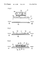
- FIG. 1 is an exploded perspective view showing an essential part of one embodiment of this invention
- FIG. 2 is a sectional illustrative view of the FIG. 1 embodiment
- FIG. 3 is a sectional illustrative view showing a state that one IC chip is firmly fixed on a leadframe in the FIG. 1 embodiment;
- FIG. 4 is a sectional illustrative view showing that two IC chips are in connection with each other in the FIG. 1 embodiment;
- FIG. 5 is a sectional illustrative view showing by magnifying the essential part in the FIG. 1 embodiment
- FIG. 6 is a sectional illustrative view showing the FIG. 1 embodiment
- FIG. 7 is a sectional illustrative view showing another embodiment of this invention.
- FIG. 8 is a sectional illustrative view showing one example of a dummy bump sheet.
- a semiconductor device 10 as an embodiment according to this invention includes a leadframe 12 .
- the leadframe 12 has a chip-mounting base 12 a arranged in a rectangular form at a center thereof.
- the leadframe 12 is provided with a plurality of lead terminals 12 b in such a manner that they extend outward from each of four sides of this mounting base 12 a .
- a main chip 14 is mounted by die-bonding.
- the main chip 14 is formed with a plurality of circuit elements 14 a , such as active elements and passive elements, at a center in a surface thereof. Surrounding the circuit elements 14 a , a plurality of electrode pads 14 b are formed for connection to a sub-chip 16 . Further, a plurality of electrode pads 14 c are formed at around the electrode pads 14 b so that they can be wire-bonded to the lead terminals 12 b . That is, the electrode pads 14 b are arranged at an periphery of a connecting area of the main IC 14 , while the electrode pads 14 c are placed at a periphery of the main chip 14 .
- circuit elements 14 a such as active elements and passive elements
- the main chip 14 has the sub-chip 16 mounted thereon so that their surfaces face to each other.
- This sub-chip 16 also has, at a main surface, a plurality of circuit elements 16 a , such as active elements and passive elements, similarly to the main chip 14 .
- a plurality of bumps 16 b are formed for connection to the electrode pads 14 b provided on the main chip 14 .
- the sub-chip 16 in this embodiment, is smaller than the main chip 14 , so that the main chip 14 is allowed to have an area corresponding to the entire area of the sub-chip 16 , thus constituting the above-stated connecting area.
- the above-stated bumps 16 b are arranged at a periphery of the IC chip 16 correspondingly in position to the electrode pads 14 b .
- the bumps 16 b are formed by plating or evaporating with solder (Pb-Sn), gold (Au), or the like so that they project toward the main surface or the connecting surface of the main chip 14 , as will be particularly well understood in FIG. 5 .
- At least one dummy bumps 16 c are formed in a connecting surface of the sub-chip 16 at an area excepting the area having the bump 16 b , specifically at a central area surrounded by the bumps 16 b , by a process similar to that of the bumps 14 b .
- These dummy bumps 16 c are also formed in a manner projecting toward the main surface or connecting surface of the main chip 14 .
- the dummy bump 16 c has a projecting height, preferably, the same in amount as the projecting height of the bump 16 b .
- the height of the dummy bump 16 c may be formed different from the height of the connecting bump 16 b . In such a case, the height of the dummy bump 16 c would be lower than the height of the connecting bump 16 b.
- the dummy bumps 16 c in this embodiment were formed of a same material as that of the connecting bump 16 b.
- the dummy bumps 16 c and the connecting bumps 16 b may be different in material.
- the connecting bumps 16 b should be formed of an electrically-conductive material, because it is to be connected to the electrode pad 14 a .
- the dummy bumps 16 c can be formed not limited only to a conductive material but also an insulating material or a semiconductor material, because it is inherently not for a purpose of electrical connection.
- the dummy bumps 16 c serve as spacers given between the main chip 14 and the sub-chip 16 , it is possible to arbitrarily select a best suited material therefor in conformity to the functional requirement.
- the bumps 16 b are formed of gold
- the dummy bumps 16 c can be formed of an inexpensive solder.
- the dummy bumps 16 c were formed in the same size (diameter, height, etc) as the connecting bumps 16 b .
- the dummy bumps 16 c may be formed different in size and/or shape from the connecting bumps 16 b .
- the connecting bumps 16 were formed in circular in plan by taking account the connection to the electrode pad 14 b through a connecting sheet 18 or anisotropic conductive sheet.
- the dummy bumps 16 c are not utilized for connection, and may be in an arbitrary form, such as rectangular, triangular, or the like, in plan.
- the connecting bumps 16 b were each formed as a projection with a round given at a tip in consideration of connection.
- the dummy bumps 16 c may be formed in a flat face at the tip.
- a connecting sheet 18 is interposed between the main chip 14 and the sub-chip 16 , as shown in FIG. 1 and FIG. 2 .
- This connecting sheet 18 is for adhering between the main chip 14 and the sub-chip, to electrically connect the connecting bumps 16 b and the electrode pads 14 b therebetween. Consequently, the connecting sheet 18 is preferably formed by an anisotropic conductive sheet.
- the anisotropic conductive sheet is made by mixing conductive particles in an adhesive resin therefor. When the bumps 16 b are strongly pressed onto the electrode pads 14 b , the conductive particles existing therebetween are brought into a contact state. Due to this, the anisotropic conductive sheet 18 becomes exhibiting electrical conductivity only in a thickness direction.
- the sub-chip 16 is placed with its main surface, i.e. the surface formed with the circuit elements 16 a and the bumps 16 b , faced down.
- the sub-chip 16 is mounted on the main chip 14 through the connecting sheet 18 such that the bumps 16 b on the sub-chip 16 respectively in abutment against the electrode pads 14 b on the main chip 14 .
- the entire assembly is heated up while pressing the sub-chip 16 onto the main chip 14 , the bumps 16 b and the electrode pads 14 b are brought into electric connection through the connecting sheet 18 .
- the adhesive resin of the connecting sheet 18 is hardened, thereby firmly fixing the sub-chip 16 on the main chip 14 .
- wire bonding is made using thin metal wires 20 between the electrode pads 14 c formed on the main chip 14 and the lead terminals 12 b of the leadframe 12 , thus providing electrical connection.
- the lead terminals 12 b are cut out of the leadframe 12 , and the lead terminals 12 b are bent into a form flush with a backside of the package 22 , thereby completing a semiconductor device 10 .
- the bumps 16 b and 16 c function as spacers present between the main chip 14 and the sub-chip 16 . This serves to suppress the warp in the main chip 14 and/or the sub-chip 16 to a minimum degree.
- a semiconductor device 10 according to an embodiment as shown in FIG. 7 is similar to the semiconductor device 10 shown in FIG. 1 and FIG. 6, except for the following point. More specifically, the FIG. 6 embodiment has electrical connection between the main chip 14 and the sub-chip 16 by providing the electrode pads 14 b on the former and the connecting pads 16 b and the dummy bumps 16 c on the latter. In the FIG. 7 embodiment, however, the main chip 14 has connecting bumps 14 b ′ modified from the electrode pads 14 b , and the dummy bumps 14 c ′ formed at a central area of a connecting surface of the main chip 14 at position corresponding to the dummy bumps 16 c of the sub-chips 16 .
- the main chips 14 and the sub-chip 16 are electrically connected through the connecting bumps 14 b ′ and 16 b , while the dummy bumps 14 c ′ and 16 c ′ function as spacers interposed between the two IC chips 14 and 16 .
- either one of the dummy bumps 14 c ′ or 16 c ′ may be provided by making modification to the FIG. 7 embodiment so that the height thereof is matched to a total height of the two connecting bumps 14 b ′ and 16 b.
- the connecting bumps 16 b (and 14 b ′) and the dummy bumps 16 c (and 14 c ′) were formed through the common process.
- a dummy bump sheet 24 as shown in FIG. 8 is utilized. That is, the dummy bump sheet 24 is made, for example, of a synthetic resin or metal to have an appropriate number of dummy bumps 24 a on a surface thereof. Where this dummy bump sheet 24 is used, this dummy bump sheet 24 may merely be adhered onto a required area on a required chip in a process separate from that for the connecting bumps 16 (and 14 b ′).
Landscapes
- Engineering & Computer Science (AREA)
- Microelectronics & Electronic Packaging (AREA)
- Power Engineering (AREA)
- Computer Hardware Design (AREA)
- Physics & Mathematics (AREA)
- Condensed Matter Physics & Semiconductors (AREA)
- General Physics & Mathematics (AREA)
- Manufacturing & Machinery (AREA)
- Wire Bonding (AREA)
Abstract
A semiconductor device includes a main chip and a sub-chip. The both chips are in a mount-structure, and molded by a resin package. The main chip has electrode pads formed at an periphery in a connecting surface thereof, while the sub-chip has a plurality of connecting bumps formed at a periphery in a connecting surface at positions corresponding to the plurality of electrode pads. A plurality of dummy bumps are formed at a central area of the connecting surface of the sub-chip. Connections are made respectively between the connecting bumps and the connecting electrodes. The main chip and the sub-chip have the connecting bumps and dummy bumps interposed therebetween to thereby prevent the main chip and/or the sub-chip from warping.
Description
1. Field of the Invention
This invention relates to a semiconductor device having a plurality of semiconductor chips. More particularly, this invention relates to a semiconductor device having one semiconductor chip stacked thereon with another semiconductor chip so that they are connected together, thereby increasing the integration density.
2. Description of the Prior Art
There is one example of this kind of a conventional semiconductor device disclosed by Japanese Laying-Open Patent Publication No. H6-112402 [H01L25/065, 07, 18] assigned to the same assignee as this invention was assigned to. This prior art includes two IC chips each having bumps formed at a periphery of a connecting surface so that the two IC chips are connected together. These both IC chips are further transfer-molded into a mold or package.
In this prior art, however, the bumps are placed only at the periphery of the IC chip, involving a problem as stated below. That is, no bumps are provided at a central area of the IC chips so that a gap might occur between the central areas of the two IC chips. This results in warping in at least one of the two IC chips in a manner of nearing two IC chips together. Accordingly, there arises a problem that the circuit elements formed in the connection surface undergo damage due to nearing the two IC chips, besides the warped IC chip surface suffers from cracks. This tendency becomes prominent as the area of the IC chips increases.
Therefore, it is a primary object of this invention to provide a novel semiconductor device having a plurality of semiconductor chips.
It is another object of this invention to provide a semiconductor device that can prevent the semiconductor chip from warping.
It is further object of this invention to provide a semiconductor device having semiconductor chips and circuit elements prevented from being damaged.
A semiconductor device according to this invention, comprises: a first semiconductor chip having a first connecting surface; a second semiconductor chip placed over the first semiconductor chip and having a second connecting surface; a plurality of first bumps formed on at least one of the first connecting surface and the second connecting surface so as to connect between the first semiconductor chip and the second semiconductor chip; and at least one second bumps formed at least one of the first connecting surface and the second connecting surface.
The first bumps serve to connect between the first connecting surface and the second connecting surface, i.e., the first semiconductor chip and the second semiconductor chip. The second bumps are interposed, at an area other than that having the first bumps, between the first semiconductor chip and the second semiconductor chip. Therefore, even if a warp occurs in one or both of the first semiconductor chip and the second semiconductor chip, the deformation is suppressed to a minimum extent.
Therefore, according to this invention, it is possible to prevent the semiconductor chip from excessively warping so that there is no possibility of damaging to the semiconductor chip or circuit elements formed thereon.
Incidentally, the first bumps solely may be utilized to connect between the first semiconductor chip and the second semiconductor chip. Alternatively to this, both the first bumps and the second bumps may be used for the connection. Note that the first bump (and the second bump) serving to connect between chips is referred to as “connecting bump” while the second bump not serving to connect between the chips is referred to as “dummy bump” throughout this Specification.
The above described objects and other objects, features, aspects and advantages of the present invention will become more apparent from the following detailed description of the present invention when taken in conjunction with the accompanying drawings.
FIG. 1 is an exploded perspective view showing an essential part of one embodiment of this invention;
FIG. 2 is a sectional illustrative view of the FIG. 1 embodiment;
FIG. 3 is a sectional illustrative view showing a state that one IC chip is firmly fixed on a leadframe in the FIG. 1 embodiment;
FIG. 4 is a sectional illustrative view showing that two IC chips are in connection with each other in the FIG. 1 embodiment;
FIG. 5 is a sectional illustrative view showing by magnifying the essential part in the FIG. 1 embodiment;
FIG. 6 is a sectional illustrative view showing the FIG. 1 embodiment;
FIG. 7 is a sectional illustrative view showing another embodiment of this invention; and
FIG. 8 is a sectional illustrative view showing one example of a dummy bump sheet.
Referring to FIG. 1 and FIG. 2, a semiconductor device 10 as an embodiment according to this invention includes a leadframe 12. The leadframe 12 has a chip-mounting base 12 a arranged in a rectangular form at a center thereof. The leadframe 12 is provided with a plurality of lead terminals 12 b in such a manner that they extend outward from each of four sides of this mounting base 12 a. On a surface of the mounting base 12 a, a main chip 14 is mounted by die-bonding.
The main chip 14 is formed with a plurality of circuit elements 14 a, such as active elements and passive elements, at a center in a surface thereof. Surrounding the circuit elements 14 a, a plurality of electrode pads 14 b are formed for connection to a sub-chip 16. Further, a plurality of electrode pads 14 c are formed at around the electrode pads 14 b so that they can be wire-bonded to the lead terminals 12 b. That is, the electrode pads 14 b are arranged at an periphery of a connecting area of the main IC 14, while the electrode pads 14 c are placed at a periphery of the main chip 14.
The main chip 14 has the sub-chip 16 mounted thereon so that their surfaces face to each other. This sub-chip 16 also has, at a main surface, a plurality of circuit elements 16 a, such as active elements and passive elements, similarly to the main chip 14. Surrounding the circuit elements 16 a, a plurality of bumps 16 b are formed for connection to the electrode pads 14 b provided on the main chip 14. The sub-chip 16, in this embodiment, is smaller than the main chip 14, so that the main chip 14 is allowed to have an area corresponding to the entire area of the sub-chip 16, thus constituting the above-stated connecting area. Accordingly, the above-stated bumps 16 b are arranged at a periphery of the IC chip 16 correspondingly in position to the electrode pads 14 b. The bumps 16 b are formed by plating or evaporating with solder (Pb-Sn), gold (Au), or the like so that they project toward the main surface or the connecting surface of the main chip 14, as will be particularly well understood in FIG. 5.
At least one dummy bumps 16 c (four in this embodiment) are formed in a connecting surface of the sub-chip 16 at an area excepting the area having the bump 16 b, specifically at a central area surrounded by the bumps 16 b, by a process similar to that of the bumps 14 b. These dummy bumps 16 c are also formed in a manner projecting toward the main surface or connecting surface of the main chip 14. The dummy bump 16 c has a projecting height, preferably, the same in amount as the projecting height of the bump 16 b. However, the height of the dummy bump 16 c may be formed different from the height of the connecting bump 16 b. In such a case, the height of the dummy bump 16 c would be lower than the height of the connecting bump 16 b.
Further, the dummy bumps 16 c in this embodiment were formed of a same material as that of the connecting bump 16 b. However, the dummy bumps 16 c and the connecting bumps 16 b may be different in material. Specifically, the connecting bumps 16 b should be formed of an electrically-conductive material, because it is to be connected to the electrode pad 14 a. Contrary to this, the dummy bumps 16 c can be formed not limited only to a conductive material but also an insulating material or a semiconductor material, because it is inherently not for a purpose of electrical connection. The dummy bumps 16 c serve as spacers given between the main chip 14 and the sub-chip 16, it is possible to arbitrarily select a best suited material therefor in conformity to the functional requirement. For example, where the bumps 16 b are formed of gold, the dummy bumps 16 c can be formed of an inexpensive solder.
Also, in the embodiment the dummy bumps 16 c were formed in the same size (diameter, height, etc) as the connecting bumps 16 b. However, the dummy bumps 16 c may be formed different in size and/or shape from the connecting bumps 16 b. For example, it can be considered that the dummy bumps 16 c be formed by far greater than a diameter of the connecting bump 16 b. Also, the connecting bumps 16 were formed in circular in plan by taking account the connection to the electrode pad 14 b through a connecting sheet 18 or anisotropic conductive sheet. Contrary to this, the dummy bumps 16 c are not utilized for connection, and may be in an arbitrary form, such as rectangular, triangular, or the like, in plan. Further, the connecting bumps 16 b were each formed as a projection with a round given at a tip in consideration of connection. However, the dummy bumps 16 c may be formed in a flat face at the tip.
In this embodiment, a connecting sheet 18 is interposed between the main chip 14 and the sub-chip 16, as shown in FIG. 1 and FIG. 2. This connecting sheet 18 is for adhering between the main chip 14 and the sub-chip, to electrically connect the connecting bumps 16 b and the electrode pads 14 b therebetween. Consequently, the connecting sheet 18 is preferably formed by an anisotropic conductive sheet. The anisotropic conductive sheet is made by mixing conductive particles in an adhesive resin therefor. When the bumps 16 b are strongly pressed onto the electrode pads 14 b, the conductive particles existing therebetween are brought into a contact state. Due to this, the anisotropic conductive sheet 18 becomes exhibiting electrical conductivity only in a thickness direction.
As shown in FIG. 2, the sub-chip 16 is placed with its main surface, i.e. the surface formed with the circuit elements 16 a and the bumps 16 b, faced down. The sub-chip 16 is mounted on the main chip 14 through the connecting sheet 18 such that the bumps 16 b on the sub-chip 16 respectively in abutment against the electrode pads 14 b on the main chip 14. When the entire assembly is heated up while pressing the sub-chip 16 onto the main chip 14, the bumps 16 b and the electrode pads 14 b are brought into electric connection through the connecting sheet 18. At the same time, the adhesive resin of the connecting sheet 18 is hardened, thereby firmly fixing the sub-chip 16 on the main chip 14.
Further, wire bonding is made using thin metal wires 20 between the electrode pads 14 c formed on the main chip 14 and the lead terminals 12 b of the leadframe 12, thus providing electrical connection.
Then, transfer-molding is carried out, as shown in FIG. 6, to form a synthetic-resin package 22 encapsulating the entire assembly. As shown in FIG. 6, the lead terminals 12 b are cut out of the leadframe 12, and the lead terminals 12 b are bent into a form flush with a backside of the package 22, thereby completing a semiconductor device 10.
During forming the package 22 or in a state of a complete semiconductor device 10, where an external force is applied to the main chip 14 and/or the sub-chip in a direction closing together the main chip 14 and sub-chip 16, if the dummy bumps 16 c are absent, there is a possibility that the main chip 14 and/or the sub-chip 16 be deformed by warping. In the above embodiment, on the contrary, the bumps 16 b and 16 c, particularly the dummy bumps 16 c, function as spacers present between the main chip 14 and the sub-chip 16. This serves to suppress the warp in the main chip 14 and/or the sub-chip 16 to a minimum degree.
A semiconductor device 10 according to an embodiment as shown in FIG. 7 is similar to the semiconductor device 10 shown in FIG. 1 and FIG. 6, except for the following point. More specifically, the FIG. 6 embodiment has electrical connection between the main chip 14 and the sub-chip 16 by providing the electrode pads 14 b on the former and the connecting pads 16 b and the dummy bumps 16 c on the latter. In the FIG. 7 embodiment, however, the main chip 14 has connecting bumps 14 b′ modified from the electrode pads 14 b, and the dummy bumps 14 c′ formed at a central area of a connecting surface of the main chip 14 at position corresponding to the dummy bumps 16 c of the sub-chips 16.
In this FIG. 6 embodiment, therefore, the main chips 14 and the sub-chip 16 are electrically connected through the connecting bumps 14 b′ and 16 b, while the dummy bumps 14 c′ and 16 c′ function as spacers interposed between the two IC chips 14 and 16.
Incidentally, either one of the dummy bumps 14 c′ or 16 c′ may be provided by making modification to the FIG. 7 embodiment so that the height thereof is matched to a total height of the two connecting bumps 14 b′ and 16 b.
In the above embodiment, the connecting bumps 16 b (and 14 b′) and the dummy bumps 16 c (and 14 c′) were formed through the common process. However, it is possible to form the connecting bumps 16 b (and 14 b′) by a conventionally-known process and the dummy bumps 16 c (and 14 c′) through a separate process therefrom. Specifically, a dummy bump sheet 24 as shown in FIG. 8 is utilized. That is, the dummy bump sheet 24 is made, for example, of a synthetic resin or metal to have an appropriate number of dummy bumps 24 a on a surface thereof. Where this dummy bump sheet 24 is used, this dummy bump sheet 24 may merely be adhered onto a required area on a required chip in a process separate from that for the connecting bumps 16 (and 14 b′).
Although the present invention has been described and illustrated in detail, it is clearly understood that the same is by way of illustration and example only and is not to be taken by way of limitation, the spirit and scope of the present invention being limited only by the terms of the appended claims.
Claims (12)
1. A semiconductor device, comprising:
a first semiconductor chip having a first connecting surface;
a second semiconductor chip arranged over said first semiconductor chip and having a second connecting surface;
a plurality of connecting members formed on at least one of the first connecting surface and the second connecting surface;
a plurality of connecting bumps formed on at least one of the first connecting surface and the second connecting surface, the connecting bumps being aligned with said connecting members so as to connect between said first semiconductor chip and said second semiconductor chip through pressure connection of said connecting bumps and said connecting members; and
at least one first dummy bump formed on at least one of the first connecting surface and the second connecting surface for spacing said first semiconductor chip from said second semiconductor chip, said at least one first dummy bump being formed at a location where said connecting members are not formed, the at least one first dummy bump being surrounded by the plurality of connecting bumps within an area defined by the plurality of connecting bumps such that the plurality of connecting bumps are accessible from a periphery of at least one of the first connecting surface and the second connecting surface, the at least one first dummy bump being formed as a sheet.
2. A semiconductor device according to claim 1, further comprising an anisotropic conductive sheet interposed between the first connecting surface and the second connecting surface.
3. A semiconductor device according to claim 2, wherein said anisotropic conductive member includes an adhesive resin sheet containing electrically conductive particles mixed therein.
4. A semiconductor device according to claim 1, further comprising a package encapsulating said first semiconductor chip and said second semiconductor chip.
5. A semiconductor device according to claim 1, wherein said at least one first dummy bump is formed at a second area that is at least one area in the first connecting surface and the second connecting surface, excepting the area having said connecting bumps in the first area.
6. A semiconductor device according to claim 5, wherein said second area is within said first area.
7. A semiconductor device according to claim 6, wherein said second area is surrounded by said first area.
8. A semiconductor device according to claim 1, wherein said connecting members include electrode pads.
9. A semiconductor device according to claim 1, wherein said connecting members include at least one second connecting bump.
10. A semiconductor device according to claim 9, further comprising at least one second dummy bump formed on at least one of the first connecting surface and the second connecting surface at positions corresponding to said at least one first dummy bump, wherein said at least one second dummy bump functions as a spacer between said first semiconductor chip and said second semiconductor chip in cooperation with said at least one first dummy bump, wherein said plurality of connecting bumps and said at least one second dummy bump are formed by a substantially similar process, and wherein said plurality of connecting bumps and said at least one second dummy bump are formed in a substantially similar shape.
11. A semiconductor device according to claim 1, wherein said at least one first dummy bump is formed at a central area of at least one of the first connecting surface and the second connecting surface.
12. A semiconductor device, comprising:
a first semiconductor chip having a first connecting surface;
a second semiconductor chip arranged over the first semiconductor chip and having a second connecting surface;
a plurality of connecting members formed substantially along a periphery of at least one of the first connecting surface and the second connecting surface;
a plurality of connecting bumps formed substantially along a periphery of at least one of the first connecting surface and the second connecting surface, the connecting bumps being aligned with and corresponding to the connecting members; and
at least one dummy bump formed at a central area inward of the periphery of at least one of the first connecting surface and the second connecting surface, the at least one dummy bump being surrounded by the plurality of connecting bumps within an area defined by the plurality of connecting bumps such that the plurality of connecting bumps are accessible from the periphery of at least one of the first connecting surface and the second connecting surface, the at least one dummy bump being formed as a sheet, the at least one dummy bump spacing the first semiconductor chip from the second semiconductor chip and suppressing warping of at least one of the first and second semiconductor chips.
Applications Claiming Priority (2)
| Application Number | Priority Date | Filing Date | Title |
|---|---|---|---|
| JP9-068540 | 1997-03-21 | ||
| JP06854097A JP3349058B2 (en) | 1997-03-21 | 1997-03-21 | Structure of a semiconductor device having a plurality of IC chips |
Publications (1)
| Publication Number | Publication Date |
|---|---|
| US6175157B1 true US6175157B1 (en) | 2001-01-16 |
Family
ID=13376688
Family Applications (1)
| Application Number | Title | Priority Date | Filing Date |
|---|---|---|---|
| US09/045,135 Expired - Lifetime US6175157B1 (en) | 1997-03-21 | 1998-03-20 | Semiconductor device package for suppressing warping in semiconductor chips |
Country Status (2)
| Country | Link |
|---|---|
| US (1) | US6175157B1 (en) |
| JP (1) | JP3349058B2 (en) |
Cited By (47)
| Publication number | Priority date | Publication date | Assignee | Title |
|---|---|---|---|---|
| US6285084B1 (en) * | 1999-02-09 | 2001-09-04 | Rohm Co., Ltd. | Semiconductor device |
| US6376914B2 (en) * | 1999-12-09 | 2002-04-23 | Atmel Corporation | Dual-die integrated circuit package |
| US20020052105A1 (en) * | 1999-08-31 | 2002-05-02 | Salman Akram | Chip package with grease heat sink and method of making |
| US6426559B1 (en) * | 2000-06-29 | 2002-07-30 | National Semiconductor Corporation | Miniature 3D multi-chip module |
| US6462420B2 (en) * | 1999-02-12 | 2002-10-08 | Rohm Co., Ltd. | Semiconductor chip and semiconductor device having a chip-on-chip structure |
| US6483190B1 (en) * | 1999-10-20 | 2002-11-19 | Fujitsu Limited | Semiconductor chip element, semiconductor chip element mounting structure, semiconductor chip element mounting device and mounting method |
| US20030038356A1 (en) * | 2001-08-24 | 2003-02-27 | Derderian James M | Semiconductor devices including stacking spacers thereon, assemblies including the semiconductor devices, and methods |
| US6537855B2 (en) * | 1999-04-28 | 2003-03-25 | Matsushita Electric Industrial Co., Ltd. | Semiconductor device and method of manufacturing the same |
| US6583512B2 (en) * | 2000-12-26 | 2003-06-24 | Matsushita Electric Industrial Co., Ltd. | Semiconductor device and method for fabricating the same |
| US6590286B2 (en) * | 2001-04-19 | 2003-07-08 | Mitsubishi Denki Kabushiki Kaisha | Land grid array semiconductor device |
| US20030173679A1 (en) * | 2002-03-13 | 2003-09-18 | Levardo Melvin N. | Stacked dice standoffs |
| US20030193088A1 (en) * | 2002-04-15 | 2003-10-16 | Micron Technology, Inc. | Semiconductor integrated circuit package having electrically disconnected solder balls for mounting |
| US20040104476A1 (en) * | 2001-07-19 | 2004-06-03 | Naofumi Iwamoto | Method of manufacturing semiconductor chip having supporting member and semiconductor package having the semiconductor chip |
| US20040124539A1 (en) * | 2002-12-31 | 2004-07-01 | Advanced Semiconductor Engineering, Inc. | Multi-chip stack flip-chip package |
| US6815832B2 (en) * | 2001-09-28 | 2004-11-09 | Rohm Co., Ltd. | Semiconductor device having opposed and connected semiconductor chips with lateral deviation confirming electrodes |
| US20040241908A1 (en) * | 2001-06-26 | 2004-12-02 | Samsung Electronics Co., Ltd. | Semiconductor package with semiconductor chips stacked therein and method of making the package |
| WO2005003791A2 (en) * | 2003-06-27 | 2005-01-13 | Formfactor, Inc. | Insulative covering of probe tips |
| US20050006730A1 (en) * | 2003-07-07 | 2005-01-13 | Motorola, Inc. | Semiconductor component and method of manufacturing same |
| US20050029642A1 (en) * | 2003-07-30 | 2005-02-10 | Minoru Takaya | Module with embedded semiconductor IC and method of fabricating the module |
| US20050042796A1 (en) * | 1998-03-27 | 2005-02-24 | Sigurd Wagner | Method for making multilayer thin-film electronics |
| US20050242431A1 (en) * | 1999-08-17 | 2005-11-03 | Agere Systems Inc. | Integrated circuit dies |
| US20050250303A1 (en) * | 2002-07-05 | 2005-11-10 | Industrial Technology Research Institute | Method for bonding IC chips to substrates incorporating dummy bumps and non-conductive adhesive |
| US20060057341A1 (en) * | 2004-09-16 | 2006-03-16 | Tdk Corporation | Multilayer substrate and manufacturing method thereof |
| US20070023903A1 (en) * | 2005-08-01 | 2007-02-01 | Seiko Epson Corporation | Semiconductor device, electronic module, and method of manufacturing electronic module |
| US20070172981A1 (en) * | 2006-01-20 | 2007-07-26 | Meng-Jen Wang | Method for making flip chip on leadframe package |
| US20070209835A1 (en) * | 2006-01-05 | 2007-09-13 | Hyeon-Ho Song | Semiconductor device having pad structure capable of reducing failures in mounting process |
| US20080096294A1 (en) * | 2006-10-24 | 2008-04-24 | Yao-Ren Liu | Integrated circuit structure, display module, and inspection method thereof |
| US20080223609A1 (en) * | 2007-03-14 | 2008-09-18 | Fujitsu Limited | Electronic device and electronic component mounting method |
| US7449771B1 (en) * | 2002-06-10 | 2008-11-11 | Asat Ltd. | Multiple leadframe laminated IC package |
| CN100438007C (en) * | 2005-02-07 | 2008-11-26 | 恩益禧电子股份有限公司 | Interconnecting substrate and semiconductor device |
| EP2009697A1 (en) * | 2007-06-27 | 2008-12-31 | Société Française de Détecteurs Infrarouges - SOFRADIR | Fabrication process of a matrix-shaped radiation detector and process for exchanging single detection modules of this matrix |
| US20090014870A1 (en) * | 2007-07-12 | 2009-01-15 | United Microelectronics Corp. | Semiconductor chip and package process for the same |
| US20090102049A1 (en) * | 2006-03-27 | 2009-04-23 | Katsumasa Murata | Semiconductor device, layered type semiconductor device using the same, base substrate and semiconductor device manufacturing method |
| US7544537B2 (en) | 2005-09-28 | 2009-06-09 | Tdk Corporation | Semiconductor IC-embedded substrate and method for manufacturing same |
| US20090212406A1 (en) * | 2008-02-22 | 2009-08-27 | Panasonic Corporation | Semiconductor device and method of manufacturing the same |
| US20090242255A1 (en) * | 2008-03-27 | 2009-10-01 | Ibiden Co., Ltd | Wiring board with built-in electronic component and method of manufacturing same |
| US20110095418A1 (en) * | 2009-10-26 | 2011-04-28 | Hwan-Sik Lim | Semiconductor package and method for fabricating the same |
| US20110233771A1 (en) * | 2010-03-26 | 2011-09-29 | Samsung Electronics Co., Ltd. | Semiconductor packages having warpage compensation |
| US20130026623A1 (en) * | 2011-07-29 | 2013-01-31 | Taiwan Semiconductor Manufacturing Company, Ltd. | Semiconductor Devices, Packaging Methods and Structures |
| US20130075853A1 (en) * | 2006-06-15 | 2013-03-28 | Pavan Gupta | Stacked Die Package for MEMS Resonator System |
| US20130159950A1 (en) * | 2011-12-16 | 2013-06-20 | Industrial Technology Research Institute | Method and apparatus of an integrated circuit |
| CN103208501A (en) * | 2012-01-17 | 2013-07-17 | 奥林巴斯株式会社 | Solid-state imaging device, imaging apparatus, substrate, semiconductor device and method of manufacturing the solid-state imaging device |
| US8887110B1 (en) * | 2007-08-22 | 2014-11-11 | Cadence Design Systems, Inc. | Methods for designing intergrated circuits with automatically synthesized clock distribution networks |
| US8981574B2 (en) | 2012-12-20 | 2015-03-17 | Samsung Electronics Co., Ltd. | Semiconductor package |
| US20150103499A1 (en) * | 2012-10-05 | 2015-04-16 | Murata Manufacturing Co., Ltd. | Electronic component-embedded module and communication terminal device |
| US9543276B2 (en) | 2014-08-22 | 2017-01-10 | Samsung Electronics Co., Ltd. | Chip-stacked semiconductor package |
| WO2018098647A1 (en) * | 2016-11-30 | 2018-06-07 | 深圳修远电子科技有限公司 | Integrated circuit multichip stacked packaging structure and method |
Families Citing this family (4)
| Publication number | Priority date | Publication date | Assignee | Title |
|---|---|---|---|---|
| US6724084B1 (en) | 1999-02-08 | 2004-04-20 | Rohm Co., Ltd. | Semiconductor chip and production thereof, and semiconductor device having semiconductor chip bonded to solid device |
| JP3405697B2 (en) | 1999-09-20 | 2003-05-12 | ローム株式会社 | Semiconductor chip |
| US6146984A (en) * | 1999-10-08 | 2000-11-14 | Agilent Technologies Inc. | Method and structure for uniform height solder bumps on a semiconductor wafer |
| KR102556518B1 (en) * | 2018-10-18 | 2023-07-18 | 에스케이하이닉스 주식회사 | Semiconductor package including supporting block supporting upper chip stack |
Citations (8)
| Publication number | Priority date | Publication date | Assignee | Title |
|---|---|---|---|---|
| US4764804A (en) * | 1986-02-21 | 1988-08-16 | Hitachi, Ltd. | Semiconductor device and process for producing the same |
| US5120665A (en) * | 1988-12-05 | 1992-06-09 | Hitachi Chemical Company | Method of using an anisotropically electroconductive adhesive having pressure-deformable electroconductive particles to electrically connect circuits |
| US5376825A (en) * | 1990-10-22 | 1994-12-27 | Seiko Epson Corporation | Integrated circuit package for flexible computer system alternative architectures |
| US5400950A (en) * | 1994-02-22 | 1995-03-28 | Delco Electronics Corporation | Method for controlling solder bump height for flip chip integrated circuit devices |
| US5523628A (en) * | 1994-08-05 | 1996-06-04 | Hughes Aircraft Company | Apparatus and method for protecting metal bumped integrated circuit chips during processing and for providing mechanical support to interconnected chips |
| US5686703A (en) * | 1994-12-16 | 1997-11-11 | Minnesota Mining And Manufacturing Company | Anisotropic, electrically conductive adhesive film |
| US5734199A (en) * | 1995-12-18 | 1998-03-31 | Matsushita Electric Industrial Co., Ltd. | Semiconductor device having improved test electrodes |
| US5813870A (en) * | 1996-07-12 | 1998-09-29 | International Business Machines Corporation | Selectively filled adhesives for semiconductor chip interconnection and encapsulation |
-
1997
- 1997-03-21 JP JP06854097A patent/JP3349058B2/en not_active Expired - Fee Related
-
1998
- 1998-03-20 US US09/045,135 patent/US6175157B1/en not_active Expired - Lifetime
Patent Citations (8)
| Publication number | Priority date | Publication date | Assignee | Title |
|---|---|---|---|---|
| US4764804A (en) * | 1986-02-21 | 1988-08-16 | Hitachi, Ltd. | Semiconductor device and process for producing the same |
| US5120665A (en) * | 1988-12-05 | 1992-06-09 | Hitachi Chemical Company | Method of using an anisotropically electroconductive adhesive having pressure-deformable electroconductive particles to electrically connect circuits |
| US5376825A (en) * | 1990-10-22 | 1994-12-27 | Seiko Epson Corporation | Integrated circuit package for flexible computer system alternative architectures |
| US5400950A (en) * | 1994-02-22 | 1995-03-28 | Delco Electronics Corporation | Method for controlling solder bump height for flip chip integrated circuit devices |
| US5523628A (en) * | 1994-08-05 | 1996-06-04 | Hughes Aircraft Company | Apparatus and method for protecting metal bumped integrated circuit chips during processing and for providing mechanical support to interconnected chips |
| US5686703A (en) * | 1994-12-16 | 1997-11-11 | Minnesota Mining And Manufacturing Company | Anisotropic, electrically conductive adhesive film |
| US5734199A (en) * | 1995-12-18 | 1998-03-31 | Matsushita Electric Industrial Co., Ltd. | Semiconductor device having improved test electrodes |
| US5813870A (en) * | 1996-07-12 | 1998-09-29 | International Business Machines Corporation | Selectively filled adhesives for semiconductor chip interconnection and encapsulation |
Cited By (109)
| Publication number | Priority date | Publication date | Assignee | Title |
|---|---|---|---|---|
| US20050042796A1 (en) * | 1998-03-27 | 2005-02-24 | Sigurd Wagner | Method for making multilayer thin-film electronics |
| US7115983B2 (en) * | 1998-03-27 | 2006-10-03 | The Trustees Of Princeton University | Multilayer, thin-film electronic devices |
| US6285084B1 (en) * | 1999-02-09 | 2001-09-04 | Rohm Co., Ltd. | Semiconductor device |
| US6462420B2 (en) * | 1999-02-12 | 2002-10-08 | Rohm Co., Ltd. | Semiconductor chip and semiconductor device having a chip-on-chip structure |
| US6537855B2 (en) * | 1999-04-28 | 2003-03-25 | Matsushita Electric Industrial Co., Ltd. | Semiconductor device and method of manufacturing the same |
| US7541674B2 (en) * | 1999-08-17 | 2009-06-02 | Agere Systems Inc. | Integrated circuit die for wire bonding and flip-chip mounting |
| US20050242431A1 (en) * | 1999-08-17 | 2005-11-03 | Agere Systems Inc. | Integrated circuit dies |
| US6972494B1 (en) * | 1999-08-17 | 2005-12-06 | Agere Systems Inc. | Integrated circuit die for wire bonding and flip-chip mounting |
| US20060097381A1 (en) * | 1999-08-31 | 2006-05-11 | Salman Akram | Chip package with grease heat sink |
| US20050001312A1 (en) * | 1999-08-31 | 2005-01-06 | Micron Technology | Chip package with grease heat sink |
| US20050221533A1 (en) * | 1999-08-31 | 2005-10-06 | Salman Akram | Method of making chip package with grease heat sink |
| US6919220B2 (en) | 1999-08-31 | 2005-07-19 | Micron Technology, Inc. | Method of making chip package with grease heat sink |
| US6424033B1 (en) * | 1999-08-31 | 2002-07-23 | Micron Technology, Inc. | Chip package with grease heat sink and method of making |
| US20020052105A1 (en) * | 1999-08-31 | 2002-05-02 | Salman Akram | Chip package with grease heat sink and method of making |
| US6794749B2 (en) | 1999-08-31 | 2004-09-21 | Micron Technology, Inc. | Chip package with grease heat sink |
| US20030057552A1 (en) * | 1999-10-20 | 2003-03-27 | Fujitsu Limited | Semiconductor chip element, semiconductor chip element mounting structure, semiconductor chip element mounting device and mounting method |
| US6483190B1 (en) * | 1999-10-20 | 2002-11-19 | Fujitsu Limited | Semiconductor chip element, semiconductor chip element mounting structure, semiconductor chip element mounting device and mounting method |
| US7436062B2 (en) | 1999-10-20 | 2008-10-14 | Fujitsu Limited | Semiconductor chip element, semiconductor chip element mounting structure, semiconductor chip element mounting device and mounting method |
| US6376914B2 (en) * | 1999-12-09 | 2002-04-23 | Atmel Corporation | Dual-die integrated circuit package |
| US6426559B1 (en) * | 2000-06-29 | 2002-07-30 | National Semiconductor Corporation | Miniature 3D multi-chip module |
| US6583512B2 (en) * | 2000-12-26 | 2003-06-24 | Matsushita Electric Industrial Co., Ltd. | Semiconductor device and method for fabricating the same |
| US20030127722A1 (en) * | 2000-12-26 | 2003-07-10 | Matsushita Electric Industrial Co., Ltd. | Semiconductor device and method for fabricating the same |
| US6590286B2 (en) * | 2001-04-19 | 2003-07-08 | Mitsubishi Denki Kabushiki Kaisha | Land grid array semiconductor device |
| US7115441B2 (en) * | 2001-06-26 | 2006-10-03 | Samsung Electronics Co., Ltd. | Semiconductor package with semiconductor chips stacked therein and method of making the package |
| US20040241908A1 (en) * | 2001-06-26 | 2004-12-02 | Samsung Electronics Co., Ltd. | Semiconductor package with semiconductor chips stacked therein and method of making the package |
| US6841462B2 (en) * | 2001-07-19 | 2005-01-11 | Oki Electric Industry Co., Ltd. | Method of manufacturing semiconductor chip having supporting member |
| US20040104476A1 (en) * | 2001-07-19 | 2004-06-03 | Naofumi Iwamoto | Method of manufacturing semiconductor chip having supporting member and semiconductor package having the semiconductor chip |
| US20030038356A1 (en) * | 2001-08-24 | 2003-02-27 | Derderian James M | Semiconductor devices including stacking spacers thereon, assemblies including the semiconductor devices, and methods |
| US20040200885A1 (en) * | 2001-08-24 | 2004-10-14 | Derderian James M | Methods for assembling semiconductor devices in stacked arrangements by positioning spacers therebetween |
| US8101459B2 (en) * | 2001-08-24 | 2012-01-24 | Micron Technology, Inc. | Methods for assembling semiconductor devices in stacked arrangements by positioning spacers therebetween |
| US6815832B2 (en) * | 2001-09-28 | 2004-11-09 | Rohm Co., Ltd. | Semiconductor device having opposed and connected semiconductor chips with lateral deviation confirming electrodes |
| US6753613B2 (en) * | 2002-03-13 | 2004-06-22 | Intel Corporation | Stacked dice standoffs |
| US20030173679A1 (en) * | 2002-03-13 | 2003-09-18 | Levardo Melvin N. | Stacked dice standoffs |
| US20030193088A1 (en) * | 2002-04-15 | 2003-10-16 | Micron Technology, Inc. | Semiconductor integrated circuit package having electrically disconnected solder balls for mounting |
| US7468559B2 (en) | 2002-04-15 | 2008-12-23 | Micron Technology, Inc. | Semiconductor integrated circuit package having electrically disconnected solder balls for mounting |
| US20080142950A1 (en) * | 2002-04-15 | 2008-06-19 | Micron Technology, Inc. | Semiconductor integrated circuit package having electrically disconnected solder balls for mounting |
| US7342319B2 (en) | 2002-04-15 | 2008-03-11 | Micron Technology, Inc. | Semiconductor integrated circuit package having electrically disconnected solder balls for mounting |
| US7268067B2 (en) | 2002-04-15 | 2007-09-11 | Micron Technology, Inc. | Semiconductor integrated circuit package having electrically disconnected solder balls for mounting |
| US7276802B2 (en) * | 2002-04-15 | 2007-10-02 | Micron Technology, Inc. | Semiconductor integrated circuit package having electrically disconnected solder balls for mounting |
| US20050026327A1 (en) * | 2002-04-15 | 2005-02-03 | Micron Technology, Inc. | Semiconductor integrated circuit package having electrically disconnected solder balls for mounting |
| US7851907B2 (en) | 2002-04-15 | 2010-12-14 | Micron Technology, Inc. | Semiconductor integrated circuit package having electrically disconnected solder balls for mounting |
| US20060237845A1 (en) * | 2002-04-15 | 2006-10-26 | Micron Technology, Inc. | Semiconductor integrated circuit package having electrically disconnected solder balls for mounting |
| US20060237844A1 (en) * | 2002-04-15 | 2006-10-26 | Micron Technology, Inc. | Semiconductor integrated circuit package having electrically disconnected solder balls for mounting |
| US7449771B1 (en) * | 2002-06-10 | 2008-11-11 | Asat Ltd. | Multiple leadframe laminated IC package |
| US20050250303A1 (en) * | 2002-07-05 | 2005-11-10 | Industrial Technology Research Institute | Method for bonding IC chips to substrates incorporating dummy bumps and non-conductive adhesive |
| US7300865B2 (en) * | 2002-07-05 | 2007-11-27 | Industrial Technology Research Institute | Method for bonding IC chips to substrates incorporating dummy bumps and non-conductive adhesive |
| US20040124539A1 (en) * | 2002-12-31 | 2004-07-01 | Advanced Semiconductor Engineering, Inc. | Multi-chip stack flip-chip package |
| US6861761B2 (en) * | 2002-12-31 | 2005-03-01 | Advanced Semiconductor Engineering Inc. | Multi-chip stack flip-chip package |
| WO2005003791A3 (en) * | 2003-06-27 | 2006-04-13 | Formfactor Inc | Insulative covering of probe tips |
| WO2005003791A2 (en) * | 2003-06-27 | 2005-01-13 | Formfactor, Inc. | Insulative covering of probe tips |
| US7074647B2 (en) * | 2003-07-07 | 2006-07-11 | Freescale Semiconductor, Inc. | Semiconductor component comprising leadframe, semiconductor chip and integrated passive component in vertical relationship to each other |
| US20050006730A1 (en) * | 2003-07-07 | 2005-01-13 | Motorola, Inc. | Semiconductor component and method of manufacturing same |
| US7547975B2 (en) * | 2003-07-30 | 2009-06-16 | Tdk Corporation | Module with embedded semiconductor IC and method of fabricating the module |
| US20050029642A1 (en) * | 2003-07-30 | 2005-02-10 | Minoru Takaya | Module with embedded semiconductor IC and method of fabricating the module |
| US7868464B2 (en) | 2004-09-16 | 2011-01-11 | Tdk Corporation | Multilayer substrate and manufacturing method thereof |
| US20060057341A1 (en) * | 2004-09-16 | 2006-03-16 | Tdk Corporation | Multilayer substrate and manufacturing method thereof |
| CN100438007C (en) * | 2005-02-07 | 2008-11-26 | 恩益禧电子股份有限公司 | Interconnecting substrate and semiconductor device |
| US7582967B2 (en) * | 2005-08-01 | 2009-09-01 | Seiko Epson Corporation | Semiconductor device, electronic module, and method of manufacturing electronic module |
| US20070023903A1 (en) * | 2005-08-01 | 2007-02-01 | Seiko Epson Corporation | Semiconductor device, electronic module, and method of manufacturing electronic module |
| US7544537B2 (en) | 2005-09-28 | 2009-06-09 | Tdk Corporation | Semiconductor IC-embedded substrate and method for manufacturing same |
| US20070209835A1 (en) * | 2006-01-05 | 2007-09-13 | Hyeon-Ho Song | Semiconductor device having pad structure capable of reducing failures in mounting process |
| US7425468B2 (en) * | 2006-01-20 | 2008-09-16 | Advanced Semiconductor Engineering, Inc. | Method for making flip chip on leadframe package |
| US20070172981A1 (en) * | 2006-01-20 | 2007-07-26 | Meng-Jen Wang | Method for making flip chip on leadframe package |
| US20090102049A1 (en) * | 2006-03-27 | 2009-04-23 | Katsumasa Murata | Semiconductor device, layered type semiconductor device using the same, base substrate and semiconductor device manufacturing method |
| US20130075853A1 (en) * | 2006-06-15 | 2013-03-28 | Pavan Gupta | Stacked Die Package for MEMS Resonator System |
| US10723617B2 (en) | 2006-06-15 | 2020-07-28 | Sitime Corporation | Package structure for micromechanical resonator |
| US8941247B1 (en) * | 2006-06-15 | 2015-01-27 | Sitime Corporation | Stacked die package for MEMS resonator system |
| US11708264B2 (en) | 2006-06-15 | 2023-07-25 | Sitime Corporation | Stacked-die MEMS resonator |
| US8669664B2 (en) * | 2006-06-15 | 2014-03-11 | Sitime Corporation | Stacked die package for MEMS resonator system |
| US20150035090A1 (en) * | 2006-06-15 | 2015-02-05 | Sitime Corporation | Stacked die package for mems resonator system |
| US11370656B2 (en) | 2006-06-15 | 2022-06-28 | Sitime Corporation | Stacked-die MEMS resonator |
| US9371221B2 (en) | 2006-06-15 | 2016-06-21 | Sitime Corporation | Low-profile stacked-die MEMS resonator system |
| US10913655B2 (en) | 2006-06-15 | 2021-02-09 | Sitime Corporation | Manufacturing of integrated circuit resonator |
| US9821998B2 (en) | 2006-06-15 | 2017-11-21 | SiTime Corpoaration | Stacked-die MEMS resonator system |
| US10287162B2 (en) | 2006-06-15 | 2019-05-14 | Sitime Corporation | Low-profile stacked-die MEMS resonator system |
| US20080096294A1 (en) * | 2006-10-24 | 2008-04-24 | Yao-Ren Liu | Integrated circuit structure, display module, and inspection method thereof |
| US20080223609A1 (en) * | 2007-03-14 | 2008-09-18 | Fujitsu Limited | Electronic device and electronic component mounting method |
| US20090004760A1 (en) * | 2007-06-27 | 2009-01-01 | Societe Francaise De Detecteurs Infrarouges-Sofradir | Method for producing a matrix for detecting electromagnetic radiation and method for replacing an elementary module of such a detection matrix |
| FR2918212A1 (en) * | 2007-06-27 | 2009-01-02 | Fr De Detecteurs Infrarouges S | METHOD FOR PRODUCING AN ELECTROMAGNETIC RADIATION MATRIX AND METHOD FOR REPLACING AN ELEMENTARY MODULE OF SUCH A DETECTION MATRIX |
| EP2009697A1 (en) * | 2007-06-27 | 2008-12-31 | Société Française de Détecteurs Infrarouges - SOFRADIR | Fabrication process of a matrix-shaped radiation detector and process for exchanging single detection modules of this matrix |
| US7811855B2 (en) | 2007-06-27 | 2010-10-12 | Societe Francaise De Detecteurs Infrarouges-Sofradir | Method for producing a matrix for detecting electromagnetic radiation and method for replacing an elementary module of such a detection matrix |
| US20090014870A1 (en) * | 2007-07-12 | 2009-01-15 | United Microelectronics Corp. | Semiconductor chip and package process for the same |
| US8887110B1 (en) * | 2007-08-22 | 2014-11-11 | Cadence Design Systems, Inc. | Methods for designing intergrated circuits with automatically synthesized clock distribution networks |
| US7977790B2 (en) * | 2008-02-22 | 2011-07-12 | Panasonic Corporation | Semiconductor device and method of manufacturing the same |
| US20090212406A1 (en) * | 2008-02-22 | 2009-08-27 | Panasonic Corporation | Semiconductor device and method of manufacturing the same |
| US8347493B2 (en) * | 2008-03-27 | 2013-01-08 | Ibiden Co., Ltd. | Wiring board with built-in electronic component and method of manufacturing same |
| US20090242255A1 (en) * | 2008-03-27 | 2009-10-01 | Ibiden Co., Ltd | Wiring board with built-in electronic component and method of manufacturing same |
| US8823172B2 (en) | 2009-10-26 | 2014-09-02 | Samsung Electronics Co., Ltd. | Semiconductor package and method for fabricating the same |
| US20110095418A1 (en) * | 2009-10-26 | 2011-04-28 | Hwan-Sik Lim | Semiconductor package and method for fabricating the same |
| US8680685B2 (en) * | 2009-10-26 | 2014-03-25 | Samsung Electronics Co., Ltd. | Semiconductor package and method for fabricating the same |
| US8604614B2 (en) * | 2010-03-26 | 2013-12-10 | Samsung Electronics Co., Ltd. | Semiconductor packages having warpage compensation |
| US9048168B2 (en) | 2010-03-26 | 2015-06-02 | Samsung Electronics Co., Ltd. | Semiconductor packages having warpage compensation |
| US20110233771A1 (en) * | 2010-03-26 | 2011-09-29 | Samsung Electronics Co., Ltd. | Semiconductor packages having warpage compensation |
| US8916969B2 (en) * | 2011-07-29 | 2014-12-23 | Taiwan Semiconductor Manufacturing Company, Ltd. | Semiconductor devices, packaging methods and structures |
| US20130026623A1 (en) * | 2011-07-29 | 2013-01-31 | Taiwan Semiconductor Manufacturing Company, Ltd. | Semiconductor Devices, Packaging Methods and Structures |
| US8689160B2 (en) | 2011-12-16 | 2014-04-01 | Industrial Technology Research Institute | Method and apparatus of an integrated circuit |
| US20130159950A1 (en) * | 2011-12-16 | 2013-06-20 | Industrial Technology Research Institute | Method and apparatus of an integrated circuit |
| US8522186B2 (en) * | 2011-12-16 | 2013-08-27 | Industrial Technology Research Institute | Method and apparatus of an integrated circuit |
| CN103208501B (en) * | 2012-01-17 | 2017-07-28 | 奥林巴斯株式会社 | Solid camera head and its manufacture method, camera device, substrate, semiconductor device |
| CN103208501A (en) * | 2012-01-17 | 2013-07-17 | 奥林巴斯株式会社 | Solid-state imaging device, imaging apparatus, substrate, semiconductor device and method of manufacturing the solid-state imaging device |
| US9478520B2 (en) | 2012-01-17 | 2016-10-25 | Olympus Corporation | Solid-state imaging device, imaging apparatus, substrate, semiconductor device and method of manufacturing the solid-state imaging device |
| US20170171966A1 (en) * | 2012-10-05 | 2017-06-15 | Murata Manufacturing Co., Ltd. | Electronic component-embedded module and communication terminal device |
| US9596764B2 (en) * | 2012-10-05 | 2017-03-14 | Murata Manufacturing Co., Ltd. | Electronic component-embedded module and communication terminal device |
| US9974165B2 (en) * | 2012-10-05 | 2018-05-15 | Murata Manufacturing Co., Ltd. | Electronic component-embedded module and communication terminal device |
| US20150103499A1 (en) * | 2012-10-05 | 2015-04-16 | Murata Manufacturing Co., Ltd. | Electronic component-embedded module and communication terminal device |
| US8981574B2 (en) | 2012-12-20 | 2015-03-17 | Samsung Electronics Co., Ltd. | Semiconductor package |
| US9633973B2 (en) | 2012-12-20 | 2017-04-25 | Samsung Electronics Co., Ltd. | Semiconductor package |
| US9543276B2 (en) | 2014-08-22 | 2017-01-10 | Samsung Electronics Co., Ltd. | Chip-stacked semiconductor package |
| WO2018098647A1 (en) * | 2016-11-30 | 2018-06-07 | 深圳修远电子科技有限公司 | Integrated circuit multichip stacked packaging structure and method |
Also Published As
| Publication number | Publication date |
|---|---|
| JP3349058B2 (en) | 2002-11-20 |
| JPH10270637A (en) | 1998-10-09 |
Similar Documents
| Publication | Publication Date | Title |
|---|---|---|
| US6175157B1 (en) | Semiconductor device package for suppressing warping in semiconductor chips | |
| US7485490B2 (en) | Method of forming a stacked semiconductor package | |
| US7405104B2 (en) | Lead frame and method of producing the same, and resin-encapsulated semiconductor device and method of producing the same | |
| US6759737B2 (en) | Semiconductor package including stacked chips with aligned input/output pads | |
| US6426559B1 (en) | Miniature 3D multi-chip module | |
| US20070048903A1 (en) | Multi-chip package type semiconductor device | |
| US20070007633A1 (en) | Lead frame, resin-encapsulated semiconductor device, and method of producing the same | |
| JP2000243887A (en) | Semiconductor device and its manufacture | |
| JPH10256470A (en) | Semiconductor device | |
| JP2002270717A (en) | Semiconductor device | |
| KR100533847B1 (en) | Stacked flip chip package using carrier tape | |
| JP2001035961A (en) | Semiconductor and manufacture thereof | |
| JP2001024133A (en) | Lead frame, resin sealed semiconductor device employing it and manufacture thereof | |
| JP2000243880A (en) | Semiconductor device and its manufacture | |
| JPH10335366A (en) | Semiconductor device | |
| JP3286196B2 (en) | Structure of sealed semiconductor device having a plurality of IC chips | |
| JPH11238828A (en) | Semiconductor device of bga type package and its manufacture and packaging equipment | |
| JPH11186449A (en) | Semiconductor device and its manufacture | |
| JP2000196005A (en) | Semiconductor device | |
| KR100218335B1 (en) | Chip-sized package | |
| JP3248854B2 (en) | Structure of a semiconductor device having a plurality of IC chips | |
| JP2000091490A (en) | Semiconductor device | |
| KR100352112B1 (en) | Structure of chip-sized semiconductor package and fabricating method thereof | |
| JP3439890B2 (en) | Semiconductor device and manufacturing method thereof | |
| JPH11233676A (en) | Semiconductor device of bga-type package, manufacture thereof and mounting apparatus |
Legal Events
| Date | Code | Title | Description |
|---|---|---|---|
| AS | Assignment |
Owner name: ROHM CO., LTD., JAPAN Free format text: ASSIGNMENT OF ASSIGNORS INTEREST;ASSIGNOR:MORIFUJI, TADAHIRO;REEL/FRAME:009220/0089 Effective date: 19980512 |
|
| FEPP | Fee payment procedure |
Free format text: PAYOR NUMBER ASSIGNED (ORIGINAL EVENT CODE: ASPN); ENTITY STATUS OF PATENT OWNER: LARGE ENTITY |
|
| STCF | Information on status: patent grant |
Free format text: PATENTED CASE |
|
| FPAY | Fee payment |
Year of fee payment: 4 |
|
| FPAY | Fee payment |
Year of fee payment: 8 |
|
| FPAY | Fee payment |
Year of fee payment: 12 |