US6166946A - System and method for writing to and reading from a memory cell - Google Patents
System and method for writing to and reading from a memory cell Download PDFInfo
- Publication number
- US6166946A US6166946A US09/489,380 US48938000A US6166946A US 6166946 A US6166946 A US 6166946A US 48938000 A US48938000 A US 48938000A US 6166946 A US6166946 A US 6166946A
- Authority
- US
- United States
- Prior art keywords
- value
- bit line
- port
- line
- signal
- Prior art date
- Legal status (The legal status is an assumption and is not a legal conclusion. Google has not performed a legal analysis and makes no representation as to the accuracy of the status listed.)
- Expired - Lifetime
Links
Images


Classifications
-
- G—PHYSICS
- G11—INFORMATION STORAGE
- G11C—STATIC STORES
- G11C11/00—Digital stores characterised by the use of particular electric or magnetic storage elements; Storage elements therefor
- G11C11/21—Digital stores characterised by the use of particular electric or magnetic storage elements; Storage elements therefor using electric elements
- G11C11/34—Digital stores characterised by the use of particular electric or magnetic storage elements; Storage elements therefor using electric elements using semiconductor devices
- G11C11/40—Digital stores characterised by the use of particular electric or magnetic storage elements; Storage elements therefor using electric elements using semiconductor devices using transistors
- G11C11/41—Digital stores characterised by the use of particular electric or magnetic storage elements; Storage elements therefor using electric elements using semiconductor devices using transistors forming static cells with positive feedback, i.e. cells not needing refreshing or charge regeneration, e.g. bistable multivibrator or Schmitt trigger
- G11C11/412—Digital stores characterised by the use of particular electric or magnetic storage elements; Storage elements therefor using electric elements using semiconductor devices using transistors forming static cells with positive feedback, i.e. cells not needing refreshing or charge regeneration, e.g. bistable multivibrator or Schmitt trigger using field-effect transistors only
-
- G—PHYSICS
- G11—INFORMATION STORAGE
- G11C—STATIC STORES
- G11C8/00—Arrangements for selecting an address in a digital store
- G11C8/16—Multiple access memory array, e.g. addressing one storage element via at least two independent addressing line groups
Definitions
- the present invention generally relates to data processing techniques and, in particular, to a system and method for performing a writing operation and a reading operation on a memory cell, such as a static-random-access-memory (SRAM) cell, during the same clock cycle.
- a memory cell such as a static-random-access-memory (SRAM) cell
- SRAM cells are known in the art for storing digital bit values and are used in many electronic applications requiring data storage, such as in the internal cache memory of a microprocessor.
- Each storage element within a SRAM cell usually stores only one bit of information at a time, and storing a new value into the storage element overwrites the previous value stored in the storage element.
- the term "operation” shall refer to a write to or a read from the memory cell that is being described. If there are two or more operations that are ready to occur, then at least one of the operations should be postponed until a later clock cycle such that no more than one operation occurs during each clock cycle. However, the postponement of operations is generally undesirable since it increases the amount of time required to produce the results of the operations.
- U.S. Pat. No. 5,815,432 entitled “Single-Ended Read, Dual-Ended Write SRAM Cell,” which is incorporated herein by reference, describes a design for a SRAM cell that enables a higher frequency of operations to occur.
- the SRAM cell of the U.S. Pat. No. 5,815,432 enables two simultaneous reads of the same cell to occur. Therefore, during a single clock cycle, either two reads from an SRAM cell or one write to the SRAM cell may occur. As a result, the number of operations that utilize the same SRAM cell during a given time period is increased.
- U.S. Pat. No. 5,815,432 works well in applications that generate a large number of read operations. However, the advantages of the U.S. Pat. No. 5,815,432 are reduced in applications that utilize a large number of write operations, since the design of the U.S. Pat. No. 5,815,432 only enables read operations to simultaneously occur.
- the present invention overcomes the inadequacies and deficiencies of the prior art as discussed hereinbefore.
- the present invention provides a system and method for writing to and reading from a memory cell during the same clock cycle.
- the memory cell of the present invention utilizes a storage element, a multiplexer, first and second bit lines, first and second switching elements, and a switching mechanism.
- the storage element has a first port and a second port and maintains a value of the first port as an inverse of the value of the second port.
- the first switching element is connected to the first port and the first bit line
- the second switching element is connected to the second port and the second bit line.
- An input value to be written to the memory cell is received by the switching mechanism, which transmits the input value to one of the bit lines based on a value of a mode signal.
- the switching mechanism may invert the input value before transmitting it to the one bit line.
- the multiplexer receives the value of the other bit line and selects this value based on the value of the mode signal. The multiplexer then transmits the selected value as an output of the memory cell.
- the present invention can also be viewed as providing a method for storing data values.
- the method can be broadly conceptualized by the following steps: providing a memory cell, the memory cell having a first port connected to a first bit line via a first switching element and a second port connected to a second bit line via a second switching element; maintaining a value of the first port as an inverse of a value of the second port; receiving an input value; receiving a clock signal; precharging the first and second bit lines in response to the clock signal; storing the input value in the memory cell, via the first bit line, between consecutive precharges of the first and second bit lines; and reading, via the second bit line, a value stored in the memory cell between the consecutive precharges of the first and second bit lines.
- FIG. 1 is a diagram illustrating an SRAM cell in accordance with the prior art.
- FIG. 2 is a diagram illustrating a more detailed view of a storage element depicted in FIG. 1.
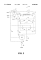
- FIG. 3 is a diagram illustrating a memory cell in accordance with the principles of the present invention.
- FIG. 4 is a diagram illustrating the graph of a clock signal and a mode signal employed to operate the memory cell of FIG. 3.
- FIG. 5 is a diagram illustrating a more detailed view of select circuitry depicted in FIG. 3.
- FIG. 6 is exemplary circuitry that may be used to control the timing of the mode signal, the read signal, and the write signal of the preferred embodiment depicted by FIG. 3.
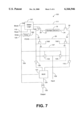
- FIG. 7 is a diagram illustrating another embodiment of a memory cell in accordance with the present invention.
- FIG. 8 is a diagram illustrating yet another embodiment of a memory cell in accordance with the present invention.
- the present invention generally provides a memory cell, such as an SRAM cell, that enables a write operation and a read operation to occur during the same clock cycle.
- a memory cell such as an SRAM cell
- FIG. 1 depicts an exemplary SRAM cell 15 of the prior art.
- a bit value is stored in a storage element 18, which has two input/output (I/O) ports 21 and 24.
- the storage element 18 is designed such that at any given time, the value at port 21 should be the inverse of the value at port 24.
- FIG. 2 depicts an exemplary embodiment of circuitry that may be used to implement the storage element 18.
- the inverters 27 ensure that the value at ports 21 and 24 are inverse to one another.
- the value at port 24 corresponds to the value stored in the storage element 18, and the value at port 21, therefore, corresponds to the inverse of the value stored in the storage element 18. For example, if the value stored in the storage element 18 is a "1," then the value at port 24 should be a logical high, and the value at port 21 should be a logical low. Conversely, if the value stored in the storage element 18 is a "0,” then the value at port 24 should be a logical low, and the value at port 21 should be a logical high. In other words, the value at port 24 represents the value stored in the storage element 18.
- the value on select line 25 is asserted to activate the switching elements 26 and 28, and the values on bit lines 32 and 34 are appropriately asserted and deasserted to write the desired value into the storage element 18.
- the storage element 18 is designed such that activation of the switching element 26 enables a logical low on bit line 32 to force the value of port 21 to a logical low and such that activation of the switching element 28 enables a logical low on bit line 34 to force the value of port 24 to a logical low.
- the storage element 18 is further designed such that a logical high on either bit line 32 or 34 does not affect the values at ports 21 and 24 and, therefore, the value stored in the storage element 18, regardless of whether the switching elements 26 and/or 28 are activated or deactivated.
- NFETs are usually used to implement the switching elements 26 and 28 as shown by FIG. 1, although it may be possible to utilize other devices in implementing the switching elements 26 and/or 28 in other embodiments.
- the select line 25 is asserted, and the bit line 32 is forced to a logical low and the bit line 34 is forced to a logical high.
- the value at port 21 is forced to a logical low, and the value at port 24 (i.e., the value representing the value stored in the storage element 18) is forced to a logical high via the inverters 27 (FIG. 2) of the storage element 18.
- the select line 25 is asserted, and the bit line 34 is forced to a logical low and the bit line 32 is forced to a logical high.
- the value at port 24 is forced to a logical low, and the value at port 21 is forced to a logical high via the inverters 27 of the storage element 18.
- Switching elements 42, 44, 46, and 48 are typically used to control the value of the bit lines 32 and 34.
- switching elements 42, 44, 46, and 48 (as well as switching elements 26 and 28) are open circuits.
- switching elements 42 and 44 allow a supply voltage (V dd ) to pass to bit lines 32 and 34, respectively, and when activated, switching elements 46 and 48 allow the values of bit lines 32 and 34 to be grounded, respectively.
- V dd supply voltage
- switching elements 46 and 48 allow the values of bit lines 32 and 34 to be grounded, respectively.
- PFETs are used to implement switching elements 42 and 44
- NFETs are used to implement switching elements 46 and 48, although other types of devices may be used to implement switching elements 42, 44, 46, and/or 48 in other embodiments.
- the precharge line 55 is asserted during a first half of a cycle of a clock signal to activate switching elements 42 and 44, and the write lines 57 and 59 are deasserted to deactivate the switching elements 46 and 48.
- the bit lines 32 and 34 are initially both forced to a logical high.
- the precharge line 55 is deasserted to deactivate the switching elements 42 and 44, and the select line 25 is asserted to activate the switching elements 26 and 28.
- one of the write lines 57 or 59 is asserted to activate the appropriate switching element 46 or 48 in order to write the desired value into the storage element 18.
- write line 57 is asserted to activate the switching element 46
- write line 59 is asserted to activate the switching element 48.
- the precharge line 55 is asserted during a first half of a cycle of the clock signal to activate the switching elements 42 and 44, and the write lines 57 and 59 are deasserted to deactivate the switching elements 46 and 48. Accordingly, the bit lines 32 and 34 are initially both forced to a logical high. Then, during the next half of the cycle of the clock signal, the precharge line 55 is deasserted to deactivate the switching elements 42 and 44, and the select line 25 is asserted to activate the switching elements 26 and 28. When the select line 25 is asserted, the port 21 or 24 having the low logical value forces the adjacent bit line 32 or 34 to a logical low.
- the bit line 32 is forced to a logical low when the select line 25 is asserted.
- the bit line 34 is forced to a logical low when the select line 25 is asserted.
- a sense amplifier 63 is configured to receive the values on bit lines 32 and 34 and to output the same value stored in the storage element 18 via output line 64 based on the values received from bit lines 32 and 34.
- the sense amplifier 63 is designed to output, via output line 64, the value received from bit line 34 as the value read from the cell 15, when the sense amplifier 63 detects a logical difference between the values on bit lines 32 and 34. Therefore, the sense amplifier 63 outputs the value received from bit line 34 as the value read from the cell 15 after the bit lines 32 and 34 have been precharged (i.e., the switching elements 42 and 44 have been activated) and one of the values on bit line 32 or 34 has been forced to a logical low after the precharge.
- a value can either be written to or read from the storage element 18 for every clock cycle.
- FIG. 3 depicts a memory cell 100, such as an SRAM cell, in accordance with the principles of the present invention.
- the memory cell 100 includes, similar to conventional memory cell 15, a storage element 18, ports 21 and 24, bit lines 32 and 34, and switching elements 26, 28, 42, and 44.
- the value stored in the storage element 18 is represented by the value at port 24, and the value of port 21 is an inverse of the value of port 24.
- a mode signal is provided to the cell 100 via mode line 104.
- the mode signal is preferably a clock signal having a frequency different than the clock (CK) signal used to control the timing of the cell 100, as will be discussed in further detail hereinbelow.
- the mode signal in the preferred embodiment, has a frequency that is half that of the CK signal, and the mode signal is synchronized with the CK signal. In other words, the mode signal toggles every cycle of the CK signal.
- the CK signal and the mode signal are shown in FIG. 4 as having different amplitudes for illustrative purposes, the CK signal and the mode signal may have the same amplitude in the preferred embodiment.
- the bit lines 32 and 34 are initially precharged in the first half of a cycle of the CK signal, as is done in the prior art. Then, during the next half of the cycle of the CK signal, the select logic 107 is designed to assert select line 111. In this regard, the select logic 107 receives the mode signal and a read signal via mode line 104 and a read line 116, respectively.
- the value on read line 116 is preferably a logical high when a read operation is to be performed and a logical low when a read operation is not to be performed.
- the select circuitry 107 is configured to assert the value transmitted across select line 111, thereby activating the switching element 28. This forces the logical value of bit line 34 to the logical value of the port 24 (i.e., the value stored in the memory element 18).
- the foregoing logical value is then passed through an amplifier 119 and received by a multiplexer 121.
- the amplifier 119 may be positioned before the multiplexer 121 (e.g., at the input of the multiplexer 121), as shown by FIG. 3, or after the multiplexer 121 (e.g., at the output of the multiplexer 121).
- the multiplexer 121 is configured to select the logical value received from bit line 34 and to transmit this logical value via output line 124.
- the multiplexer 121 is configured to receive the mode signal via mode line 104 as a control signal and to select the value received from bit line 34 when the mode signal is a logical high.
- the multiplexer 121 is configured to select the value received from bit line 32 instead and to transmit this value via output line 124.
- the value transmitted across output line 124 is received by an exclusive--or (XOR) gate 125, which also receives the mode signal from mode line 104. Therefore, when the mode signal is a logical high, the XOR gate 125 outputs the value received from output line 124. As will be later discussed, when the mode signal is a logical low, the XOR gate 125 outputs the inverse of the value received from output line 124.
- the logical value output by XOR gate 125 should be the logical value stored in storage element 18 (i.e., is the value read from memory cell 100).
- the write signal on write line 126 is preferably forced to a logical high when a write operation is to be performed and forced to a logical low when a write operation is not to be performed.
- the logical value to be written to the storage element 18 is transmitted across input line 128 when the write signal is forced to a logical high.
- the select logic 107 is configured to assert the value transmitted across select line 129, thereby activating the switching element 26 during the next half of the cycle of the CK signal.
- the mode signal is transmitted as a control signal to switching elements 133 and 135 of a switching mechanism 137.
- the switching elements 133 and 135 are tri-state amplifiers but may be any other type of switch in other embodiments.
- other configurations of the switching mechanism 137 may exist without departing from the principles of the present invention.
- the switching element 133 When the mode signal is a logical high, the switching element 133 is designed to transmit an inverse of the value from input line 128 to bit line 32. Therefore, if the value on input line 128 is a logical high, the value of bit line 32 is forced to a logical low. As a result, the value at port 21 is forced to a logical low, and the value at port 24 is, therefore, forced to a logical high (i.e., a "1" is written into the storage element 18) via the inverters 27 (FIG. 2) of the storage element 18. If the value on input line 128 is a logical low, then the value of bit line 32 is forced to a logical high, and no change occurs to the value at ports 21 and 24.
- the switching element 135 is designed to operate as an open circuit. Therefore, any value on input line 128 should not be transmitted by the switching element 135. As a result, the value being read from the cell 100 via bit line 34 should not be affected by the value on input line 128.
- the bit lines 32 and 34 are initially precharged in the first half of a cycle of CK, as is done in the prior art. Then, during the next half of the cycle of the CK signal, the select logic 107 is designed to assert select line 129 in response to the logical high on read line 116 and the logical low on mode line 104, thereby activating the switching element 26. This forces the logical value of bit line 32 to the logical value of the port 21 (i.e., the inverse of the value stored in the memory element 18).
- the logical value on bit line 32 is then passed through an amplifier 138 and received by multiplexer 121.
- the amplifier 138 may be positioned before the multiplexer 121 (e.g., at the input of the multiplexer 121), as shown by FIG. 3, or after the multiplexer 121 (e.g., at the output of the multiplexer 121).
- the multiplexer 121 is configured to select the logical value received from bit line 32 and to transmit this logical value via output line 124.
- the XOR gate 125 is configured to output an inverse of this value in response to the logical low on mode line 104. Therefore, the logical value output by XOR gate 125 should be the logical value stored in storage element 18 (i.e., is the value read from memory cell 100).
- a write operation may be simultaneously performed using bit line 34.
- the write signal on write line 126 is preferably forced to a logical high, and the logical value to be written to the storage element 18 is transmitted across input line 128.
- the select logic 107 is configured to assert the value transmitted across select line 111, thereby activating the switching element 28 during the last half of a cycle of the CK signal (i.e., after bit lines 32 and 34 have been precharged).
- the mode signal is transmitted via mode line 104 as a control signal to switching elements 133 and 135.
- the switching element 135 is designed to transmit the value from input line 128 to bit line 34. Therefore, if the value on input line 128 is a logical low, the value of bit line 34 is forced to a logical low. As a result, the value at port 24 is forced to a logical low (i.e., a "0" is written into the storage element 18), and the value at port 21 is, therefore, forced to a logical high via the inverters 27 (FIG. 2) of the storage element 18. If the value on input line 128 is a logical high, then the value of bit line 34 is forced to a logical high, and no change occurs to the value at ports 21 and 24.
- the switching element 133 is designed to operate as an open circuit. Therefore, any value on the input line 128 should not be transmitted by the switching element 133. As a result, the value being read from the cell 100 via bit line 32 should not be affected by the value on input line 128.
- FIG. 5 shows exemplary circuitry that may be used to implement the select logic 107.
- the select logic 107 shown by FIG. 5 includes AND gates 142, 143, 144 and 145 and includes OR gates 146 and 147.
- the AND gate 142 and OR gate 146 are configured to assert the value transmitted across select line 111, if the read signal on read line 116 is a logical high. If the read signal on read line 116 is a logical low when the mode signal is a logical high, then AND gates 142 and 143 and the OR gate 146 are designed to deassert the value transmitted across select line 111.
- the AND gate 145 and OR gate 147 are configured to assert the value transmitted across select line 129, if the write signal on write line 126 is a logical high. If the write signal on write line 126 is a logical low when the mode signal is a logical high, then AND gates 144 and 145 and the OR gate 147 are designed to deassert the value transmitted across select line 129.
- the AND gate 143 and OR gate 146 are configured to assert the value transmitted across select line 111, if the write signal on write line 126 is a logical high. If the write signal on write line 126 is a logical low when the mode signal is a logical low, then AND gates 142 and 143 and the OR gate 146 are designed to deassert the value transmitted across select line 111.
- the AND gate 144 and OR gate 147 are configured to assert the value transmitted across select line 129, if the read signal on read line 116 is a logical high. If the read signal on read line 116 is a logical low when the mode signal is a logical low, then AND gates 144 and 145 and the OR gate 147 are designed to deassert the value transmitted across select line 129.
- FIG. 6 depicts exemplary circuitry that may be used to control the timing of the signals transmitted across lines 55, 104, 116, and 121 based on the CK signal.
- an inverse value of the CK signal is transmitted across precharge line 55 by an inverter 152. Therefore, the value on precharge line 55 is asserted during the first half of a cycle of the CK signal and is deasserted during the last half of the cycle of the CK signal.
- the switching elements 42 and 44 (FIG. 3) are activated during the first half of the cycle of the CK signal, thereby forcing the values of bit lines 32 and 34 to V dd or, in other words, to a logical high.
- the switching elements 42 and 44 are deactivated, thereby isolating bit lines 32 and 34 from V dd .
- AND gates 155 and 157 are configured to deassert the values transmitted across lines 116 and 126, respectively, regardless of the values of the read signal and the write signal respectively received from lines 161 and 163.
- the write signal on line 161 when asserted, indicates that the value on input line 128 should be written to the storage element 18 and, when deasserted, indicates that a write operation should not occur.
- the read signal on line 163, when asserted, indicates that the value stored in the storage element 18 should be output by the cell 100 and, when deasserted, indicates that no read operation should occur.
- the CK signal is a logical high in the preferred embodiment. Therefore, AND gate 155 transmits the value received from line 161 to write line 126, and AND gate 157 transmits the value received from line 163 to read line 116.
- read and write operations are enabled only in the last half of the cycle of the CK signal. In other words, read and write operations are enabled only after bit lines 32 and 34 have been precharged.
- Mode circuitry 171 is configured to receive the CK signal. Based on the CK signal, the mode circuitry 171 produces the mode signal and transmits the mode signal across mode line 104. As set forth hereinabove, the mode signal is preferably synchronized with the CK signal such that the mode signal toggles when the CK signal completes a cycle.
- the mode signal is toggled to a logical high.
- the write signal on write line 126, the read signal on read line 116, and the mode signal on mode line 104 are all set to a logical high, during the last half of a cycle of the CK signal (i.e., after bit lines 32 and 34 have been precharged).
- the select logic 107 asserts the signals on select lines 111 and 129, and the switching elements 26 and 28 are activated.
- the mode signal is a logical high
- the value stored in the storage element 18 is read via bit line 34 and the value to be written into the storage element 18 is transmitted to bit line 32. If the value to be written into the storage element 18 is a logical high, then the value of port 21 is forced to a logical low, and the value of port 24 is, therefore, forced to a logical high. As a result, the write operation and the read operation are performed during the same cycle of the CK signal.
- the mode signal toggles to a logical low, and the value on input line 128 (i.e., the value to be written into the storage element 18) is maintained on input line 128. Furthermore, the value of the write signal on line 126 is maintained at a logical high. Therefore, during the last half of this next cycle of the CK signal, the value of select line 111 is asserted, thereby activating switching element 28. Since the mode signal is now a logical low, the value to be written into the storage element 18 is transmitted to bit line 34 via switching element 135.
- the value to be written into the storage element 18 by a write operation is written into the storage element 18 in one of the foregoing two cycles of the CK signal. It is possible to also perform a different read operation in each of these two cycles. Therefore, by utilizing the techniques described hereinabove, it is possible to increase the number of operations performed on the memory cell 100.
- the present invention has been described hereinabove as utilizing a storage element having two ports 21 and 24 from which to read and write data.
- the present invention should not be so limited.
- multi-ported memory cells are well known in the art, and it is possible for the memory cell 100 of the present invention to include other storage elements 18 and/or other ports 21 and/or 24.
- the write operation may be delayed a sufficient amount of time to ensure that the write operation does not overwrite the data read by the read operation.
- the write signal transmitted to select logic 107 via write connection 126 may pass through a delay mechanism 182.
- the delay mechanism 182 is designed to delay the write signal a sufficient amount of time to ensure that the write operation does not overwrite the data read by any read operations occurring during the same cycle of the CK signal.
- the read and write operation occurring during the same cycle of the CK signal may be prevented from accessing the same storage element 18.
- at least one other storage element 18' is included in the memory cell 100, as shown by FIG. 8.
- the storage element 18' is configured identical to storage element 18 and, therefore, includes two ports 21' and 24'.
- the value at port 21' should be the inverse of the value at port 24', and the value at port 24' represents the value stored in the storage element 18'.
- the cell 100 depicted by FIG. 8 also includes select logic 107' that is configured identical to select logic 107. Therefore, the select logic 107' controls the states of switching elements 26' and 28' based on a read' signal and a write' signal respectively received from connections 116' and 126' in the same way that select logic 107 controls the states of switching elements 26 and 28 based on a read signal and a write signal respectively received from connections 116 and 126.
- a read operation may be performed on one of the storage elements 18 or 18' via one of the bit lines 32 or 34 while a write operation is performed on the other of the storage elements 18 or 18' via the other bit line 32 or 34.
- the value written to the cell 100 via the write operation should not overwrite the value read from the cell 100 via the read operation, even though the two operations are simultaneously performed.
Abstract
Description
Claims (19)
Priority Applications (2)
| Application Number | Priority Date | Filing Date | Title |
|---|---|---|---|
| US09/489,380 US6166946A (en) | 2000-01-21 | 2000-01-21 | System and method for writing to and reading from a memory cell |
| JP2001012879A JP3541179B2 (en) | 2000-01-21 | 2001-01-22 | System and method for writing to and reading from memory cells |
Applications Claiming Priority (1)
| Application Number | Priority Date | Filing Date | Title |
|---|---|---|---|
| US09/489,380 US6166946A (en) | 2000-01-21 | 2000-01-21 | System and method for writing to and reading from a memory cell |
Publications (1)
| Publication Number | Publication Date |
|---|---|
| US6166946A true US6166946A (en) | 2000-12-26 |
Family
ID=23943615
Family Applications (1)
| Application Number | Title | Priority Date | Filing Date |
|---|---|---|---|
| US09/489,380 Expired - Lifetime US6166946A (en) | 2000-01-21 | 2000-01-21 | System and method for writing to and reading from a memory cell |
Country Status (2)
| Country | Link |
|---|---|
| US (1) | US6166946A (en) |
| JP (1) | JP3541179B2 (en) |
Cited By (15)
| Publication number | Priority date | Publication date | Assignee | Title |
|---|---|---|---|---|
| US20030081449A1 (en) * | 2001-11-01 | 2003-05-01 | Dale Beucler | Method and apparatus for providing pseudo 2-port RAM functionality using a 1-port memory cell |
| US6567326B2 (en) * | 2000-08-09 | 2003-05-20 | Kabushiki Kaisha Toshiba | Semiconductor memory device |
| US20050195641A1 (en) * | 2004-03-02 | 2005-09-08 | Anderson Scott A. | Memory system and associated methodology |
| US20060262635A1 (en) * | 2005-05-20 | 2006-11-23 | Matsushita Electric Industrial Co., Ltd. | Semiconductor memory device |
| US20070242529A1 (en) * | 2005-03-15 | 2007-10-18 | Jason Redgrave | Method and Apparatus for Accessing Contents of Memory Cells |
| US7872496B2 (en) | 2004-02-14 | 2011-01-18 | Tabula, Inc. | Method of mapping a user design defined for a user design cycle to an IC with multiple sub-cycle reconfigurable circuits |
| US20110018582A1 (en) * | 2007-09-06 | 2011-01-27 | Trevis Chandler | Configuration context switcher with a clocked storage element |
| CN1941174B (en) * | 2005-09-28 | 2012-01-11 | 海力士半导体有限公司 | Multi-port memory device |
| US8112468B1 (en) | 2007-03-22 | 2012-02-07 | Tabula, Inc. | Method and apparatus for performing an operation with a plurality of sub-operations in a configurable IC |
| US8183882B2 (en) | 2004-11-08 | 2012-05-22 | Tabula, Inc. | Reconfigurable IC that has sections running at different reconfiguration rates |
| US8705310B2 (en) | 2012-08-24 | 2014-04-22 | Cypress Semiconductor Corporation | Access methods and circuits for memory devices having multiple banks |
| US20140232292A1 (en) * | 2013-02-15 | 2014-08-21 | Osram Sylvania Inc. | Illumination techniques and devices |
| US20160358645A1 (en) * | 2013-07-25 | 2016-12-08 | Renesas Electronics Corporation | Semiconductor integrated circuit device |
| US9576630B2 (en) | 2010-07-09 | 2017-02-21 | Cypress Semiconductor Corporation | Memory devices and methods having multiple address accesses in same cycle |
| US9640237B1 (en) | 2012-08-24 | 2017-05-02 | Cypress Semiconductor Corporation | Access methods and circuits for memory devices having multiple channels and multiple banks |
Citations (5)
| Publication number | Priority date | Publication date | Assignee | Title |
|---|---|---|---|---|
| US5034923A (en) * | 1987-09-10 | 1991-07-23 | Motorola, Inc. | Static RAM with soft defect detection |
| US5353251A (en) * | 1992-09-21 | 1994-10-04 | Sharp Kabushiki Kaisha | Memory cell circuit with single bit line latch |
| US5450353A (en) * | 1993-08-02 | 1995-09-12 | Nec Corporation | Static random access memory device having reset controller |
| US5781469A (en) * | 1997-01-24 | 1998-07-14 | Atmel Corporation | Bitline load and precharge structure for an SRAM memory |
| US5815432A (en) * | 1997-07-10 | 1998-09-29 | Hewlett-Packard Company | Single-ended read, dual-ended write SCRAM cell |
-
2000
- 2000-01-21 US US09/489,380 patent/US6166946A/en not_active Expired - Lifetime
-
2001
- 2001-01-22 JP JP2001012879A patent/JP3541179B2/en not_active Expired - Fee Related
Patent Citations (5)
| Publication number | Priority date | Publication date | Assignee | Title |
|---|---|---|---|---|
| US5034923A (en) * | 1987-09-10 | 1991-07-23 | Motorola, Inc. | Static RAM with soft defect detection |
| US5353251A (en) * | 1992-09-21 | 1994-10-04 | Sharp Kabushiki Kaisha | Memory cell circuit with single bit line latch |
| US5450353A (en) * | 1993-08-02 | 1995-09-12 | Nec Corporation | Static random access memory device having reset controller |
| US5781469A (en) * | 1997-01-24 | 1998-07-14 | Atmel Corporation | Bitline load and precharge structure for an SRAM memory |
| US5815432A (en) * | 1997-07-10 | 1998-09-29 | Hewlett-Packard Company | Single-ended read, dual-ended write SCRAM cell |
Cited By (29)
| Publication number | Priority date | Publication date | Assignee | Title |
|---|---|---|---|---|
| US6567326B2 (en) * | 2000-08-09 | 2003-05-20 | Kabushiki Kaisha Toshiba | Semiconductor memory device |
| US6882562B2 (en) * | 2001-11-01 | 2005-04-19 | Agilent Technologies, Inc. | Method and apparatus for providing pseudo 2-port RAM functionality using a 1-port memory cell |
| US20030081449A1 (en) * | 2001-11-01 | 2003-05-01 | Dale Beucler | Method and apparatus for providing pseudo 2-port RAM functionality using a 1-port memory cell |
| US8193830B2 (en) | 2004-02-14 | 2012-06-05 | Tabula, Inc. | Configurable circuits, IC's, and systems |
| US7872496B2 (en) | 2004-02-14 | 2011-01-18 | Tabula, Inc. | Method of mapping a user design defined for a user design cycle to an IC with multiple sub-cycle reconfigurable circuits |
| US20050195641A1 (en) * | 2004-03-02 | 2005-09-08 | Anderson Scott A. | Memory system and associated methodology |
| US7035134B2 (en) * | 2004-03-02 | 2006-04-25 | Hewlett-Packard Development Company, L.P. | Memory system and associated methodology |
| US8183882B2 (en) | 2004-11-08 | 2012-05-22 | Tabula, Inc. | Reconfigurable IC that has sections running at different reconfiguration rates |
| US20070242529A1 (en) * | 2005-03-15 | 2007-10-18 | Jason Redgrave | Method and Apparatus for Accessing Contents of Memory Cells |
| US7804730B2 (en) * | 2005-03-15 | 2010-09-28 | Tabula, Inc. | Method and apparatus for accessing contents of memory cells |
| US7366007B2 (en) * | 2005-05-20 | 2008-04-29 | Matsushita Electric Industrial Co., Ltd. | Semiconductor memory device |
| US20060262635A1 (en) * | 2005-05-20 | 2006-11-23 | Matsushita Electric Industrial Co., Ltd. | Semiconductor memory device |
| CN1941174B (en) * | 2005-09-28 | 2012-01-11 | 海力士半导体有限公司 | Multi-port memory device |
| US8112468B1 (en) | 2007-03-22 | 2012-02-07 | Tabula, Inc. | Method and apparatus for performing an operation with a plurality of sub-operations in a configurable IC |
| US8138789B2 (en) | 2007-09-06 | 2012-03-20 | Tabula, Inc. | Configuration context switcher with a clocked storage element |
| US20110018582A1 (en) * | 2007-09-06 | 2011-01-27 | Trevis Chandler | Configuration context switcher with a clocked storage element |
| US8344755B2 (en) | 2007-09-06 | 2013-01-01 | Tabula, Inc. | Configuration context switcher |
| US9576630B2 (en) | 2010-07-09 | 2017-02-21 | Cypress Semiconductor Corporation | Memory devices and methods having multiple address accesses in same cycle |
| US9666255B2 (en) | 2012-08-24 | 2017-05-30 | Cypress Semiconductor Corporation | Access methods and circuits for memory devices having multiple banks |
| US9640237B1 (en) | 2012-08-24 | 2017-05-02 | Cypress Semiconductor Corporation | Access methods and circuits for memory devices having multiple channels and multiple banks |
| US8705310B2 (en) | 2012-08-24 | 2014-04-22 | Cypress Semiconductor Corporation | Access methods and circuits for memory devices having multiple banks |
| US9210768B2 (en) * | 2013-02-15 | 2015-12-08 | Osram Sylvania Inc. | Illumination techniques and devices |
| US20140232292A1 (en) * | 2013-02-15 | 2014-08-21 | Osram Sylvania Inc. | Illumination techniques and devices |
| US20160358645A1 (en) * | 2013-07-25 | 2016-12-08 | Renesas Electronics Corporation | Semiconductor integrated circuit device |
| US9830977B2 (en) * | 2013-07-25 | 2017-11-28 | Renesas Electronics Corporation | Semiconductor integrated circuit device |
| US9947393B2 (en) | 2013-07-25 | 2018-04-17 | Renesas Electronics Corporation | Semiconductor integrated circuit device |
| US20180204613A1 (en) | 2013-07-25 | 2018-07-19 | Renesas Electronics Corporation | Semiconductor integrated circuit device |
| US10304527B2 (en) | 2013-07-25 | 2019-05-28 | Renesas Electronics Corporation | Semiconductor integrated circuit device |
| US10580484B2 (en) | 2013-07-25 | 2020-03-03 | Renesas Electronics Corporation | Semiconductor integrated circuit device |
Also Published As
| Publication number | Publication date |
|---|---|
| JP2001243776A (en) | 2001-09-07 |
| JP3541179B2 (en) | 2004-07-07 |
Similar Documents
| Publication | Publication Date | Title |
|---|---|---|
| US6914829B2 (en) | Multi-stage output multiplexing circuits and methods for double data rate synchronous memory devices | |
| US6166946A (en) | System and method for writing to and reading from a memory cell | |
| US6310816B2 (en) | Method and system for accessing rows in multiple memory banks within an integrated circuit | |
| US6249480B1 (en) | Fully synchronous pipelined ram | |
| US6377512B1 (en) | Clock synchronous type semiconductor memory device that can switch word configuration | |
| US20200082856A1 (en) | Dfe conditioning for write operations of a memory device | |
| KR100694440B1 (en) | A semiconductor memory | |
| US20060250884A1 (en) | Memory device and method of controlling the same | |
| US7394707B2 (en) | Programmable data strobe enable architecture for DDR memory applications | |
| US5257236A (en) | Static RAM | |
| US5815432A (en) | Single-ended read, dual-ended write SCRAM cell | |
| US6301322B1 (en) | Balanced dual-edge triggered data bit shifting circuit and method | |
| JP2007257822A (en) | Semiconductor memory device testing on/of state of odt circuit during data read mode and test method of state of odt circuit | |
| US7599237B2 (en) | Memory device and method for precharging a memory device | |
| JPH09320261A (en) | Semiconductor memory circuit and control signal generation circuit | |
| US6320794B1 (en) | Late-write type semiconductor memory device with multi-channel data output multiplexer | |
| US5825715A (en) | Method and apparatus for preventing write operations in a memory device | |
| US5774410A (en) | Semiconductor storage device | |
| WO2005091934A2 (en) | Sense amplifier systems and methods | |
| JP4383028B2 (en) | Semiconductor memory device and control method thereof | |
| EP0405411B1 (en) | Semiconductor memory having improved data readout scheme | |
| US6028448A (en) | Circuitry architecture and method for improving output tri-state time | |
| KR100613447B1 (en) | Data Latch Circuit and Semiconductor Device | |
| US6192005B1 (en) | Clock control signal and output enable signal generator in semiconductor memory device | |
| US6195296B1 (en) | Semiconductor memory device and system |
Legal Events
| Date | Code | Title | Description |
|---|---|---|---|
| AS | Assignment |
Owner name: HEWLETT-PACKARD COMPANY, COLORADO Free format text: ASSIGNMENT OF ASSIGNORS INTEREST;ASSIGNOR:NAFFZIGER, SAMUEL D.;REEL/FRAME:010810/0614 Effective date: 20000120 |
|
| STCF | Information on status: patent grant |
Free format text: PATENTED CASE |
|
| FEPP | Fee payment procedure |
Free format text: PAYOR NUMBER ASSIGNED (ORIGINAL EVENT CODE: ASPN); ENTITY STATUS OF PATENT OWNER: LARGE ENTITY |
|
| FPAY | Fee payment |
Year of fee payment: 4 |
|
| FEPP | Fee payment procedure |
Free format text: PAYER NUMBER DE-ASSIGNED (ORIGINAL EVENT CODE: RMPN); ENTITY STATUS OF PATENT OWNER: LARGE ENTITY Free format text: PAYOR NUMBER ASSIGNED (ORIGINAL EVENT CODE: ASPN); ENTITY STATUS OF PATENT OWNER: LARGE ENTITY |
|
| FPAY | Fee payment |
Year of fee payment: 8 |
|
| AS | Assignment |
Owner name: HEWLETT-PACKARD DEVELOPMENT COMPANY, L.P., TEXAS Free format text: ASSIGNMENT OF ASSIGNORS INTEREST;ASSIGNOR:HEWLETT-PACKARD COMPANY;REEL/FRAME:026945/0699 Effective date: 20030131 |
|
| FPAY | Fee payment |
Year of fee payment: 12 |
|
| AS | Assignment |
Owner name: HEWLETT PACKARD ENTERPRISE DEVELOPMENT LP, TEXAS Free format text: ASSIGNMENT OF ASSIGNORS INTEREST;ASSIGNOR:HEWLETT-PACKARD DEVELOPMENT COMPANY, L.P.;REEL/FRAME:037079/0001 Effective date: 20151027 |