US6147668A - Digital display unit of a computer system having an improved method and apparatus for sampling analog display signals - Google Patents
Digital display unit of a computer system having an improved method and apparatus for sampling analog display signals Download PDFInfo
- Publication number
- US6147668A US6147668A US09/100,503 US10050398A US6147668A US 6147668 A US6147668 A US 6147668A US 10050398 A US10050398 A US 10050398A US 6147668 A US6147668 A US 6147668A
- Authority
- US
- United States
- Prior art keywords
- delay
- signal
- clock signal
- analog
- sampling
- Prior art date
- Legal status (The legal status is an assumption and is not a legal conclusion. Google has not performed a legal analysis and makes no representation as to the accuracy of the status listed.)
- Expired - Fee Related
Links
Images

Classifications
-
- G—PHYSICS
- G09—EDUCATION; CRYPTOGRAPHY; DISPLAY; ADVERTISING; SEALS
- G09G—ARRANGEMENTS OR CIRCUITS FOR CONTROL OF INDICATING DEVICES USING STATIC MEANS TO PRESENT VARIABLE INFORMATION
- G09G5/00—Control arrangements or circuits for visual indicators common to cathode-ray tube indicators and other visual indicators
- G09G5/003—Details of a display terminal, the details relating to the control arrangement of the display terminal and to the interfaces thereto
- G09G5/006—Details of the interface to the display terminal
- G09G5/008—Clock recovery
-
- G—PHYSICS
- G09—EDUCATION; CRYPTOGRAPHY; DISPLAY; ADVERTISING; SEALS
- G09G—ARRANGEMENTS OR CIRCUITS FOR CONTROL OF INDICATING DEVICES USING STATIC MEANS TO PRESENT VARIABLE INFORMATION
- G09G5/00—Control arrangements or circuits for visual indicators common to cathode-ray tube indicators and other visual indicators
- G09G5/18—Timing circuits for raster scan displays
-
- G—PHYSICS
- G09—EDUCATION; CRYPTOGRAPHY; DISPLAY; ADVERTISING; SEALS
- G09G—ARRANGEMENTS OR CIRCUITS FOR CONTROL OF INDICATING DEVICES USING STATIC MEANS TO PRESENT VARIABLE INFORMATION
- G09G2320/00—Control of display operating conditions
- G09G2320/02—Improving the quality of display appearance
Definitions
- the present invention relates to computer graphics systems, and more specifically to a method and apparatus for sampling an analog display signal received in a digital display unit.
- Digital display units e.g., flat panel monitors
- An analog display signal generally includes display data signal (e.g., in RGB format) and corresponding synchronization signals (e.g., HSYNC and VSYNC).
- the display data signal identifies a color intensity for each point of an image and the synchronization signals provide a time reference such that each portion of the display data signal can be correlated with a corresponding portion of the image,
- Display signals are typically generated by a digital-to-analog converter (DAC) in a graphics source generally located outside of a digital display unit.
- the DAC generates a portion of a display data signal by processing each of several pixel data element values representing an image.
- Each pixel data element value generally represents the color intensity of a point of the image such that the display data signal represents the overall image.
- An analog-to-digital converter (ADC) located in a digital display unit usually samples display signals to recover the pixel data elements and display the represented images.
- ADC analog-to-digital converter
- the analog display signals received by a digital display unit are characterized by frequency components.
- signals which can change amplitude levels quickly (or sharply) include high bandwidth components, and are accordingly termed as wide bandwidth signals.
- signals which can only change slowly as a function of time may be termed as narrow-band signals.
- analog display signals be wide bandwidth signals as display signals may represent adjacent points differing substantially (e.g., no color intensity to complete brightness) in intensity level and an ideal display signals needs to transition in amplitude instantaneously to represent such adjacent points.
- stairway signal resembles a "stairway” as is (illustrated below with reference to FIG. 1A) well-known in the relevant arts.
- the input to an ADC in a digital display unit may not resemble an ideal stairway-signal for several reasons.
- DACs in typical graphics sources may not be able to generate stairway shaped signals due to practical limitations in cost and manufacturing technologies.
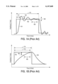
- overshoots of some magnitude are typical with transitions as illustrated with reference to FIG. 1A, which depicts a graph of a portion of display signal with amplitude on Y-Axis and time on X-Axis.
- the ideal stairway signal is shown as line 150.
- Time duration 170 represents the pixel period, which is a time duration when the signal level represents the pixel data element value from which the portion is generated.
- Time duration 110 represents a rise time as the analog signal level changes to a desired amplitude level represented by stairway signal 150.
- overshoot 120 is typically present in wide bandwidth analog display signals. The overshoot decreases substantially over time, and the overshoots are down to a large degree in the time duration 160. Therefore, time duration 160 (“sampling duration”) is a suitable period for taking samples representing the corresponding pixel data element.
- the sampled data element values can vary from the correct value represented by the ideal stairway signal 150.
- the effect is that perceptible display artifacts may be present in the displayed images.
- the artifacts may have the form of rolling diagonal bars or horizontal lines or low frequency flicker.
- Display artifacts result due to such aliased components. These type of display artifacts may be undesirable in some situations.
- An analog display signal presented to an ADC as a result of any such schemes is a signal which responds slowly to changes in the values of adjacent pixel data elements as generally illustrated with reference to FIG. 1B.
- FIG. 1B illustrates a portion of an analog display signal (corresponding to a pixel data element) generated either as an output of a low pass filter or a slow DAC. Similar time durations are represented by similar numerals in comparison to FIG. 1A. The overshoots and external noise are substantially eliminated. However, due to the jitter generally present in sampling clocks driving ADCs and the short sampling period 160 particularly with the analog display signals generated at high dot clock speeds, the sampled data values may differ substantially from the corresponding pixel data element value corresponding to the display signal portion.
- the result may be a decrease in the effective number of quantization levels in the operation of ADCs, and thus a reduction of effective number of bits (ENOB) as is well known in the relevant arts.
- ENOB effective number of bits
- an ADC can generate an 8-bit output with the ability to discriminate between 2 8 (256) color intensities (or quantization levels)
- Smaller ENOBs usually means a degradation in the display quality, and thus undesirable.
- the present invention is directed to a method and apparatus for generating a sampling clock signal for sampling an analog display signal received by a digital display unit.
- the sampling clock is generated such that display artifacts caused by high frequency noise signals may be substantially reduced (or eliminated) in the display of successive image frames encoded in a wide bandwidth analog display signal.
- a clock generator in a display unit first generates an intermediate clock signal synchronized with the synchronization signals in a received analog display signal. Due to the synchronization, the analog display signal may be generally sampled in the sampling duration if the intermediate clock signal were to be used as a sampling clock.
- the sampling clock used for sampling the analog display signal is generated in accordance with the present invention by modulating the intermediate clock by different phase delay amounts for successive image frames (or horizontal lines). Due to the different phase delays, samples are taken at different sampling points for successive image frames for the same pixel position. The amount of phase delay is maintained to be small enough such that the samples are again taken in the sampling duration.
- the effect of displaying the sampled values on many digital display units is that the image for the pixel position is perceived as if the sampled values are passed through a low-pass filter. This is because of at least one of two reasons--(1) the display units generally respond slowly to changes in image intensity, and (2) the human eye generally perceives an average intensity when a display is varied in quick succession. It may be noted that the filtering action is temporal in nature, that is, the average of intensities across a few successive frames is perceived for each pixel position (point) on a digital display screen.
- each pixel position on a display screen is perceived to have been displayed with an average of the sampled data values for the pixel position.
- the average is typically less than any samples which may consistently deviate substantially in successive image frames due to high frequency noise, display artifacts may be substantially reduced.
- all the sampled data element values may be substantially equal and no degradation in display quality is generally felt.
- the present invention provides an effective method and apparatus to reduce display artifacts which may be caused distortions (from ideal stair-way signal) present in wide-band analog display signals. This is achieved by changing the phase delay of the sampling clock minimally for successive image frames.
- the present invention is particularly suited for low-cost digital display units because only addition of integrated circuit is necessary to reduce the display artifacts.
- the present invention takes advantage of the low-pass filter naturally present with respect to human eye perception and flat-panel monitor displays to avoid the need for additional low pass filter also.
- FIG. 1A is a graph of a wide bandwidth analog signal illustrating the characteristics of a portion of the signal encoding an pixel data element value
- FIG. 1 B is a graph of a narrow bandwidth analog signal illustrating the characteristics of a portion of the signal encoding an pixel data element value
- FIG. 2 is a block diagram of a computer system illustrating an example environment in which the present invention can be implemented
- FIG. 3 is a block diagram of a digital display unit implemented in accordance with the present invention.
- FIG. 4 is a flow-chart illustrating a method in accordance with the present invention.
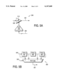
- FIG. 5A is a block diagram illustrating an analog implementation of adjustable delay block
- FIG. 5B is a block diagram illustrating another implementation of the adjustable delay block
- FIG. 6 is a flow-chart illustrating the manner in which different phase delays can be computed for successive image frames
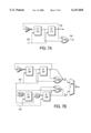
- FIG. 7A is a block diagram illustrating a circuit for generating different phase delays for successive image frames
- FIG. 7B is a block diagram illustrating another circuit for generating different phase delays which vary for each line.
- FIG. 8 is a graph of a wide bandwidth analog display signal illustrating the sampling points resulting from modulation using different phase delays.
- the present invention provides a method and apparatus for generating a sampling clock signal for sampling an analog display signal received by a digital display unit.
- the sampling clock is generated such that display artifacts caused by high frequency noise signals may be substantially reduced (or eliminated) in the display of successive image frames encoded in a wide bandwidth analog display signal. The manner in which the display artifacts are reduced is explained below first with general reference to FIG. 8.
- FIG. 8 includes potential sampling points 861-864 in addition.
- the parts of FIG. 8 already included in FIG. 1A are not described here for conciseness.
- the sampling points are located in sampling duration 160.
- signal 101 represents the display data portion for each of a few pixel data elements, with the few pixel data elements corresponding to a consecutive image frame and to the same pixel position in the image frames.
- four pixel data elements may correspond to 100 th pixel data element in 200 th row in four consecutive image frames of 640 ⁇ 480 pixels size.
- an intermediate clock signal synchronized with the synchronization signals (associated with the display data portion) is generated first. Synchronization has the general effect of ensuring that samples will be taken at a specific sampling point (assume at sampling point 862 for illustration) in samples duration 160. That is, if the intermediate clock were to be used as a sampling clock (and assuming no jitter in the sampling clock), the samples are likely to be taken at (or very close to) the specific sampling point (sampling point 862).
- a sampling clock is generated by modulating the intermediate clock signal by different phase delay amounts ("phase delta” or "modulation index") in successive frames.
- the phase delta may be modified either in successive lines or frames.
- the phase delta is maintained to be small enough such that the samples are taken in the sampling duration 160.
- the phase delta may be varied such that samples are taken at sampling points 863, 861 and 864 for the following image frames for pixel position 100 th pixel data element in 200 row.
- any samples deviating substantially from an average value in the sampling duration 160 may have less effect on the displayed image due to the sampling at different sampling points.
- an embodiment may be implemented with a low pass filter which ensures that substantial averages from the mean do not have a dominant effect on the display.
- the output of the low-pass filter may be used to generate display on a digital display screen.
- such a low pass filter may not be used in an alternative embodiment for one of two reasons--(1) the human eye generally perceives only the average color intensities when quick changes in the color intensity are presented, and (2) displays screens of digital display units generally respond slowly to changes in color intensity. As the images are scanned at rates in the range of at least 50-100 Hz in typical display units, either of these phenomenon may operate as a natural low pass filter. Accordingly, the change in the phase delay across consecutive frames may result in the reduction of display artifacts which would other wise result from the high frequency noise components in wide bandwidth signals may be accomplished without using an extra low-pass filter.
- the invention can be implemented in any computer system having a digital display unit such as a flat panel monitor.
- the present invention is described in the context of a computer system operating in graphics modes such as EGA, VGA and SVGA modes.
- Such computer systems include, without limitation, lap-top and desk-top personal computer systems, work-stations, special purpose computer systems, general purpose computer systems, network computers, and many others.
- the invention may be implemented in hardware, software, firmware, or combination of the like.
- the above noted graphics modes are described in detail in a book entitled, "Programmer's Guide to the EGA, VGA, and Super VGA Cards", published by Addition-Wesley Publishing Company, by Richard F. Ferraro, ISBN Number 0-201-62490-7, which is incorporated in its entirety herewith.
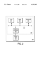
- FIG. 2 is a block diagram of computer system 200 in which the present invention can be implemented.
- Computer system 200 includes central processing unit (CPU) 210, random access memory (RAM) 220, one or more peripherals 230, graphics controller 260, and digital display unit 270.
- CPU 210, RAM 220 and graphics controller 260 are typically packaged in a single unit, and such a unit is referred to as graphics source 299 as an analog display signal is generated by the unit. All the components in graphics source 299 of computer system 200 communicate over bus 250, which can in reality include several physical buses connected by appropriate interfaces.
- RAM 220 stores data representing commands and possibly pixel data representing a source image.
- CPU 210 executes commands stored in RAM 220, and causes different commands and pixel data to be transferred to graphics controller 260.
- Peripherals 230 can include storage components such as hard-drives or removable drives (e.g., floppy-drives). Peripherals 230 can be used to store commands and/or data which enable computer system 200 to operate in accordance with the present invention. By executing the stored commands, CPU 210 provides the electrical and control signals to coordinate and control the operation of various components.
- Graphics controller 260 receives data/commands from CPU 210, generates analog display signals including display data and corresponding synchronization signals, and provides both to digital display unit 270.
- Graphics controller 260 can generate an analog display signal in the RS-170 standard with RGB signals in one embodiment.
- the analog display signal is in the form of RGB signals and the reference signal includes the VSYNC and HSYNC signals well known in the relevant arts. Therefore, three analog display signals (red, green and blue) are generated from each pixel data element.
- the present invention is described with reference to one display data signal. It should be understood that the description may be applicable to all the three display data signals. It should be further understood that the present invention can be implemented with analog image data and/or reference signals in other standards even though the present description is provided with reference to RGB signals. Examples of such standards include composite sync standard usually implemented on Macintosh Computer Systems and Sync on Green standard.
- graphics controller 260 first generates pixel data elements of a source image with a predefined width and height (measured in terms of number of pixel data elements).
- the pixel data elements for a source image may either be provided by CPU 210 or be generated by graphics controller 260 in response to commands from CPU 210.
- Graphics controller 260 typically includes a digital to analog converter (DAC) for generating an analog display signal based on the pixel data elements in a known way.
- DAC digital to analog converter
- the signals generated by DACs need to be of wide bandwidth signals particularly in view of the high image resolutions and scan rates.
- Digital display unit 270 receives an analog display signal from graphics controller 260, and processes the received display signal.
- the received analog signal may include several components which cause the analog display signal to deviation from the ideal stairway signal.
- the components may include those that cause the overshoots (resulting from high speed DACs) and those introduced by reflections due to impedance mismatches in the path from DAC to display unit 270, among others as noted above in the section entitled "Background of the Invention.”
- the display artifacts which may result from the noise components are minimized in accordance with the present invention as described below.
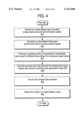
- FIG. 4 is a flow-chart illustrating a method in accordance with the present invention. For illustration, the method is described with reference to FIG. 2.
- digital display unit 270 receives an analog display signal including analog display data and synchronization signals in a known way.
- digital display unit 270 generates an intermediate clock signal synchronized with the synchronization signals. Due to such synchronization, a sampling scheme using the intermediate clock signal would sample an analog display signal in a sampling duration 160. However, the actual sampling clock is generated by modulating the intermediate clock signal as described with reference to step 430.
- step 430 digital display unit 270 generates a sampling clock by modulating the intermediate clock signal by different amounts of phase delay for successive image frames in the display signal.
- the analog display data included in the received analog display signal is sampled using the sampling clock in step 440.
- the modulation of step 430 has the general effect that sampling are taken at different points in the samples duration for the same pixel position in successive image frames. With reference to FIG. 8, 861-864 represent such different points in the sampling duration.
- step 450 digital display unit 270 processes the sampled data elements. Processing may entail steps such as resizing.
- the pixel data elements generated by the processing of step 450 can be used for generating display signals on a digital display screen in step 460. Due to the change of phase delay by different amounts in step 430, display artifacts resulting from any noise components may be reduced.
- display artifacts may be reduced in digital display units by using the method of FIG. 4.
- the method can be implemented in several embodiments as will be apparent to one skilled in the relevant arts by reading the description herein. An example embodiment is described below.
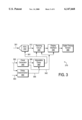
- FIG. 3 is a block diagram of digital display unit 270 illustrating an embodiment in accordance with the present invention.
- Digital display unit 270 can include ADC 310, resizing circuit, display interface 330, clock generator 340, delay determination block 350, adjustable delay 360, and digital display screen 390. Each block is described in detail below.
- ADC 310 samples analog display data received on line 301 using a sampling clock received on SCLK signal 361.
- ADC 310 may be implemented in a known way.
- Resizing circuit 320 receives the sampled data elements on line 312 from ADC 310, and upscales or downscales the image represented by the sampled data elements. Resizing circuit 320 may use clock signals from clock generator 340 for performing the resizing operation. Embodiments of upscaler are described in U.S. Pat. No. 5,739,867, entitled, "A Method and Apparatus for Upscaling an Image" issued on Apr. 4, 1998, and naming as inventor Alexander J. Eglit, which is incorporated in its entirety into the present application. The embodiments there may use SCLK signal 361 and DCLK signal 342.
- Display interface 330 receives pixel data elements representing images to be displayed from resizing circuit 330, and generates displays signals compatible with digital display screen 390.
- Display interface 330 may used DCLK signal 342 to generate the display signals to cause digital display screen 390 to generate images.
- Clock generator 340 receives horizontal synchronization signals (HSYNC) on line 302, and generates DCLK signal 342 and an intermediate clock signal on line 346.
- HSELNC horizontal synchronization signals
- a embodiment of clock generator 340 is described in the co-pending U.S. patent application entitled "A Method and Apparatus for Clock Recovery in a Digital Display Unit", Ser. No. 08/803,824, Filed Feb. 24, 1997, and is incorporated in its entirety into the present application herewith.
- Digital display screen 390 includes several pixels organized as rows and columns.
- a pixel position refers to a pixel in a given row and column.
- Several digital display screens are designed such that pixels respond slowly to changes in display intensity. That is, if the color intensity is varied during successive scans at a pixel, the change in display intensity is slow at that pixel position in the display. The slow response makes the digital display screen 390 operate as a temporal low pass filter when displaying pixels scanned with varying intensities in successive image frames.
- Adjustable delay 360 delays (or modifies in general) the intermediate clock signal by a phase delay amount which may be determined by an input received on line 356.
- Delay determination circuit 350 determines the phase delay amount. The amount of delay can be determined according to any scheme so long as the eventual sampling with the samples duration and the sampling point is generally different among consecutive frames.
- Delay determination circuit 350 and adjustable delay 360 together may be viewed as a modulation circuit, which modulates intermediate clock signal 346 by different phase delay amounts such that samples on successive frames corresponding to a given pixel position are taken at different sampling points in a sampling duration.
- Adjustable delay 360 can be implemented using analog components, digital components or the like. Example implementations are illustrated with reference to FIGS. 5A and 5B.
- FIG. 5A depicts analog variable delay 510 driven by digital to analog converter (DAC) 520.
- DAC 520 receives on line 356 an input number representing the phase delay by which an intermediate clock received on line 346 needs to be delayed.
- the output of DAC 520 is proportional to the received number, and the output voltage drives analog variable delay 510 to modulate (delay) the intermediate clock signal proportionate the input number on line 356.
- DAC 520 and variable delay 510 can be implemented using conventional components.
- FIG. 5B illustrates an another embodiment of adjustable delay 360.
- Delay elements 561-562 delay an intermediate clock signal received on line 346 preferably by equal time durations.
- the delays are typically in the range of a fraction of a nano-second (for fast sampling clock signals) to a few nano-seconds such that even the longest delayed signal from delay 563 causes sampling to be taken during the samples duration 160 (of FIG. 8). Even though only four delay elements are shown, several more delay elements may be implemented in adjustable delay 360.
- Multiplexor 550 receives as inputs the outputs of all the delay elements 561-563 and the input clock signal received on line 346. Multiplexor 550 selects one of the inputs under the control of line 356.
- the number on line 356 generally indicates the input to be selected. The number can be generated in one of several ways. Some example embodiments for generating the number are described below with reference to FIGS. 7, 6A and 6B.
- Delay determination circuit 360 can be implemented in hardware, software, firmware, or combination of the like. An example method of generating the numbers substantially in software is described with reference to FIG. 6. Embodiments implemented substantially in hardware are illustrated with reference to FIGS. 7A and 7B.
- a randomization table including a sequence of random numbers may be generated and stored in a memory (not shown) in display unit 270.
- Each random number can represent an absolute value representing delay as an input to DAC 520 in FIG. 5A, or an input to multiplexor 550 in FIG. 5B.
- the random numbers can be chosen arbitrarily or according to a pre-determined algorithm.
- a determination is made as to whether a new image frame is being received (e.g., by examining VSYNC signals).
- a new randomization number is selected from the randomization table in step 630.
- the selected value is stored in a phase delay control register (not shown) included within delay determination circuit 360.
- the phase delay control register drives adjustable delay 360. As a new number affecting the phase delay modification of the intermediate clock signals is selected for every frame, the sampling point may be different in successive frames.
- FIGS. 7A and 7B illustrate embodiments of delay determination 350 implemented in hardware. Both Figures generally depict circuits for generating random numbers, which are known well in the relevant arts.
- the embodiment of FIG. 7A changes the phase modification value once every frame, which the embodiment of FIG. 7B changes the phase modification value once every line. In either case, the sampling point is generally different for successive frames for the same pixel position.
- the simple Johnson counter depicted in FIG. 7A generates a randomization sequence of 0, 2, 1, 3, 0, 2, 1 on the two bits 749 (bit 0) and 748 (bit 1).
- Flip-flops (FFs) 710 and 711 are clocked by the VSYNC signal available on line 303.
- XOR gate 740 receives as inputs the outputs of flip-flops 710 and 711.
- Inverter 720 inverts the output of flip-flop 711 and provides the inverted value as input to flip-flop 710.
- the two bits together may be provided on bus 356 of FIG. 3.
- FIG. 7B includes two portions 791 and 792, each providing a two bit output. The two bit outputs are added by adder 795.
- Portion 791 operates similar to the circuit in FIG. 7A and is not described again for conciseness.
- Portion 792 also operates similar to the circuit of FIG. 7A except that the inputs to flip-flops 762 and 764 are provided by AND gates 780 and 781 respectively. As both the AND gates have as one of the inputs the inverted VSYNC signal, flip-flops 762 and 764 are reset at the beginning of each frame. As flip-flops 762 and 764 are clocked by HSYNC signal 302, the output of portion 792 is computed each horizontal line.
- the embodiment of FIG. 7B provides a potentially different number every horizontal line. The number can be provide as an input to multiplexor 550 to select an intermediate signal delayed by an amount corresponding to the number.
- phase of the sampling clock signal provided to ADC 310 may be changed every line or every frame in accordance with the embodiments of above.
- phase of the sampling clock due to the change of phase of the sampling clock, successive image frames encoded in an analog display signal may be sampled at different sampling points in the sampling duration. Due to the natural inclination of the human eye to perceive the average intensity of quickly changing points, and the digital display screen's general characteristic of responding slowly to changes in intensity of points while scanning, display artifacts which may otherwise result are reduced in accordance with the present invention.
Abstract
Description
Claims (15)
Priority Applications (2)
| Application Number | Priority Date | Filing Date | Title |
|---|---|---|---|
| US09/100,503 US6147668A (en) | 1998-06-20 | 1998-06-20 | Digital display unit of a computer system having an improved method and apparatus for sampling analog display signals |
| US09/655,195 US6307498B1 (en) | 1998-06-20 | 2000-09-05 | Digital display unit of a computer system having an improved method and apparatus for sampling analog display signals |
Applications Claiming Priority (1)
| Application Number | Priority Date | Filing Date | Title |
|---|---|---|---|
| US09/100,503 US6147668A (en) | 1998-06-20 | 1998-06-20 | Digital display unit of a computer system having an improved method and apparatus for sampling analog display signals |
Related Child Applications (1)
| Application Number | Title | Priority Date | Filing Date |
|---|---|---|---|
| US09/655,195 Continuation US6307498B1 (en) | 1998-06-20 | 2000-09-05 | Digital display unit of a computer system having an improved method and apparatus for sampling analog display signals |
Publications (1)
| Publication Number | Publication Date |
|---|---|
| US6147668A true US6147668A (en) | 2000-11-14 |
Family
ID=22280089
Family Applications (2)
| Application Number | Title | Priority Date | Filing Date |
|---|---|---|---|
| US09/100,503 Expired - Fee Related US6147668A (en) | 1998-06-20 | 1998-06-20 | Digital display unit of a computer system having an improved method and apparatus for sampling analog display signals |
| US09/655,195 Expired - Fee Related US6307498B1 (en) | 1998-06-20 | 2000-09-05 | Digital display unit of a computer system having an improved method and apparatus for sampling analog display signals |
Family Applications After (1)
| Application Number | Title | Priority Date | Filing Date |
|---|---|---|---|
| US09/655,195 Expired - Fee Related US6307498B1 (en) | 1998-06-20 | 2000-09-05 | Digital display unit of a computer system having an improved method and apparatus for sampling analog display signals |
Country Status (1)
| Country | Link |
|---|---|
| US (2) | US6147668A (en) |
Cited By (15)
| Publication number | Priority date | Publication date | Assignee | Title |
|---|---|---|---|---|
| US6307498B1 (en) * | 1998-06-20 | 2001-10-23 | Genesis Microchip Corp. | Digital display unit of a computer system having an improved method and apparatus for sampling analog display signals |
| US6462726B1 (en) * | 1998-02-19 | 2002-10-08 | Matsushita Electric Industrial Co., Ltd. | Video signal processor |
| US20030164897A1 (en) * | 2002-03-04 | 2003-09-04 | Chang-Lun Chen | Methods and apparatus for bridging different video formats |
| US20030189544A1 (en) * | 2002-04-09 | 2003-10-09 | Shouji Nitawaki | Display control circuit for liquid crystal display |
| US6633288B2 (en) * | 1999-09-15 | 2003-10-14 | Sage, Inc. | Pixel clock PLL frequency and phase optimization in sampling of video signals for high quality image display |
| US20040183769A1 (en) * | 2000-09-08 | 2004-09-23 | Earl Schreyer | Graphics digitizer |
| DE10254469B4 (en) * | 2002-11-21 | 2004-12-09 | Sp3D Chip Design Gmbh | Method and device for determining a frequency for sampling analog image data |
| US6876339B2 (en) * | 1999-12-27 | 2005-04-05 | Semiconductor Energy Laboratory Co., Ltd. | Semiconductor device and driving method thereof |
| US7190360B1 (en) * | 1998-08-31 | 2007-03-13 | Semiconductor Energy Laboratory Co., Ltd. | Display device and method of driving the same |
| US20070121007A1 (en) * | 2005-11-18 | 2007-05-31 | Markus Waldner | Video signal sampling system with sampling clock adjustment |
| US20070279423A1 (en) * | 2000-12-22 | 2007-12-06 | Keeney Richard A | Methods and apparatus for repairing inoperative pixels in a display |
| US20080002058A1 (en) * | 2006-06-30 | 2008-01-03 | Nec Display Solutions, Ltd. | Image display apparatus and method of adjusting clock phase |
| WO2011097801A1 (en) * | 2010-02-11 | 2011-08-18 | 北京视博数字电视科技有限公司 | Method and device for cyclically sampling, method and device for image displaying |
| US20140015868A1 (en) * | 2012-07-13 | 2014-01-16 | Semiconductor Energy Laboratory Co., Ltd. | Liquid Crystal Display Device and Method for Driving Liquid Crystal Display Device |
| CN109074784A (en) * | 2016-04-01 | 2018-12-21 | 夏普株式会社 | Display device, the control method of display device and control program |
Families Citing this family (6)
| Publication number | Priority date | Publication date | Assignee | Title |
|---|---|---|---|---|
| US6972778B2 (en) * | 2002-06-27 | 2005-12-06 | Koninklijke Philips Electronics N.V. | Color re-mapping for color sequential displays |
| US7274209B1 (en) * | 2003-06-26 | 2007-09-25 | Cypress Semiconductor Corporation | Low voltage to high voltage signal level translator with improved performance |
| KR100583723B1 (en) * | 2003-09-16 | 2006-05-25 | 삼성전자주식회사 | Apparatus for sampling a plurality of analog signals |
| US7307562B2 (en) * | 2006-02-22 | 2007-12-11 | Analog Devices, Inc. | Spectrally-adjusted sampling methods and structures for digital displays |
| US7778789B2 (en) * | 2006-07-28 | 2010-08-17 | Mediatek Inc. | Digital phase calibration method and system |
| US7602325B2 (en) * | 2007-12-28 | 2009-10-13 | General Electric Company | Sigma delta analog to digital converter with internal synchronous demodulation |
Citations (8)
| Publication number | Priority date | Publication date | Assignee | Title |
|---|---|---|---|---|
| US5739867A (en) * | 1997-02-24 | 1998-04-14 | Paradise Electronics, Inc. | Method and apparatus for upscaling an image in both horizontal and vertical directions |
| US5742799A (en) * | 1997-02-18 | 1998-04-21 | Motorola, Inc. | Method and apparatus for synchronizing multiple clocks |
| US5796392A (en) * | 1997-02-24 | 1998-08-18 | Paradise Electronics, Inc. | Method and apparatus for clock recovery in a digital display unit |
| US5821910A (en) * | 1995-05-26 | 1998-10-13 | National Semiconductor Corporation | Clock generation circuit for a display controller having a fine tuneable frame rate |
| US5841430A (en) * | 1992-01-30 | 1998-11-24 | Icl Personal Systems Oy | Digital video display having analog interface with clock and video signals synchronized to reduce image flicker |
| US5912713A (en) * | 1993-12-28 | 1999-06-15 | Canon Kabushiki Kaisha | Display control apparatus using display synchronizing signal |
| US5917461A (en) * | 1996-04-26 | 1999-06-29 | Matsushita Electric Industrial Co., Ltd. | Video adapter and digital image display apparatus |
| US5959691A (en) * | 1996-07-12 | 1999-09-28 | Samsung Electronics Co., Ltd. | Digital display apparatus having image size adjustment |
Family Cites Families (1)
| Publication number | Priority date | Publication date | Assignee | Title |
|---|---|---|---|---|
| US6147668A (en) * | 1998-06-20 | 2000-11-14 | Genesis Microchip Corp. | Digital display unit of a computer system having an improved method and apparatus for sampling analog display signals |
-
1998
- 1998-06-20 US US09/100,503 patent/US6147668A/en not_active Expired - Fee Related
-
2000
- 2000-09-05 US US09/655,195 patent/US6307498B1/en not_active Expired - Fee Related
Patent Citations (8)
| Publication number | Priority date | Publication date | Assignee | Title |
|---|---|---|---|---|
| US5841430A (en) * | 1992-01-30 | 1998-11-24 | Icl Personal Systems Oy | Digital video display having analog interface with clock and video signals synchronized to reduce image flicker |
| US5912713A (en) * | 1993-12-28 | 1999-06-15 | Canon Kabushiki Kaisha | Display control apparatus using display synchronizing signal |
| US5821910A (en) * | 1995-05-26 | 1998-10-13 | National Semiconductor Corporation | Clock generation circuit for a display controller having a fine tuneable frame rate |
| US5917461A (en) * | 1996-04-26 | 1999-06-29 | Matsushita Electric Industrial Co., Ltd. | Video adapter and digital image display apparatus |
| US5959691A (en) * | 1996-07-12 | 1999-09-28 | Samsung Electronics Co., Ltd. | Digital display apparatus having image size adjustment |
| US5742799A (en) * | 1997-02-18 | 1998-04-21 | Motorola, Inc. | Method and apparatus for synchronizing multiple clocks |
| US5739867A (en) * | 1997-02-24 | 1998-04-14 | Paradise Electronics, Inc. | Method and apparatus for upscaling an image in both horizontal and vertical directions |
| US5796392A (en) * | 1997-02-24 | 1998-08-18 | Paradise Electronics, Inc. | Method and apparatus for clock recovery in a digital display unit |
Cited By (30)
| Publication number | Priority date | Publication date | Assignee | Title |
|---|---|---|---|---|
| US6462726B1 (en) * | 1998-02-19 | 2002-10-08 | Matsushita Electric Industrial Co., Ltd. | Video signal processor |
| US6307498B1 (en) * | 1998-06-20 | 2001-10-23 | Genesis Microchip Corp. | Digital display unit of a computer system having an improved method and apparatus for sampling analog display signals |
| US7782315B2 (en) | 1998-08-31 | 2010-08-24 | Semiconductor Energy Laboratory Co., Ltd | Display device and method of driving the same |
| US20070159429A1 (en) * | 1998-08-31 | 2007-07-12 | Semiconductor Energy Laboratory Co., Ltd. | Display device and method of driving the same |
| US7190360B1 (en) * | 1998-08-31 | 2007-03-13 | Semiconductor Energy Laboratory Co., Ltd. | Display device and method of driving the same |
| US6633288B2 (en) * | 1999-09-15 | 2003-10-14 | Sage, Inc. | Pixel clock PLL frequency and phase optimization in sampling of video signals for high quality image display |
| US20040032406A1 (en) * | 1999-09-15 | 2004-02-19 | Sandeep Agarwal | Pixel clock PLL frequency and phase optimization in sampling of video signals for high quality image display |
| US6933937B2 (en) | 1999-09-15 | 2005-08-23 | Genesis Microchip Inc. | Pixel clock PLL frequency and phase optimization in sampling of video signals for high quality image display |
| US6876339B2 (en) * | 1999-12-27 | 2005-04-05 | Semiconductor Energy Laboratory Co., Ltd. | Semiconductor device and driving method thereof |
| US20040183769A1 (en) * | 2000-09-08 | 2004-09-23 | Earl Schreyer | Graphics digitizer |
| US20070279423A1 (en) * | 2000-12-22 | 2007-12-06 | Keeney Richard A | Methods and apparatus for repairing inoperative pixels in a display |
| US7071992B2 (en) | 2002-03-04 | 2006-07-04 | Macronix International Co., Ltd. | Methods and apparatus for bridging different video formats |
| US20030164897A1 (en) * | 2002-03-04 | 2003-09-04 | Chang-Lun Chen | Methods and apparatus for bridging different video formats |
| US7034796B2 (en) * | 2002-04-09 | 2006-04-25 | Oki Electric Industry Co., Ltd. | Display control circuit for liquid crystal display |
| US20030189544A1 (en) * | 2002-04-09 | 2003-10-09 | Shouji Nitawaki | Display control circuit for liquid crystal display |
| US20050179571A1 (en) * | 2002-11-21 | 2005-08-18 | Martin Maier | Method and apparatus for determining a frequency for the sampling of an analog signal |
| DE10254469B4 (en) * | 2002-11-21 | 2004-12-09 | Sp3D Chip Design Gmbh | Method and device for determining a frequency for sampling analog image data |
| US7257499B2 (en) | 2002-11-21 | 2007-08-14 | Koninklijke Philips Electronics N.V. | Method and apparatus for determining a frequency for the sampling of an analog signal |
| US20070121007A1 (en) * | 2005-11-18 | 2007-05-31 | Markus Waldner | Video signal sampling system with sampling clock adjustment |
| US20100201874A1 (en) * | 2006-06-30 | 2010-08-12 | Nec Display Solutions, Ltd. | Image display apparatus and method of adjusting clock phase |
| US20080002058A1 (en) * | 2006-06-30 | 2008-01-03 | Nec Display Solutions, Ltd. | Image display apparatus and method of adjusting clock phase |
| US8525771B2 (en) | 2006-06-30 | 2013-09-03 | Nec Display Solutions, Ltd. | Image display apparatus and method of adjusting clock phase using delay evaluation signal |
| US9262989B2 (en) * | 2006-06-30 | 2016-02-16 | Nec Display Solutions, Ltd. | Image display apparatus and method of adjusting clock phase using a delay evaluation signal |
| WO2011097801A1 (en) * | 2010-02-11 | 2011-08-18 | 北京视博数字电视科技有限公司 | Method and device for cyclically sampling, method and device for image displaying |
| CN102484725A (en) * | 2010-02-11 | 2012-05-30 | 北京视博云科技有限公司 | Method and device for cyclically sampling, method and device for image displaying |
| CN102484725B (en) * | 2010-02-11 | 2014-04-23 | 北京视博云科技有限公司 | Method for cyclically sampling, method and device for image displaying |
| US20140015868A1 (en) * | 2012-07-13 | 2014-01-16 | Semiconductor Energy Laboratory Co., Ltd. | Liquid Crystal Display Device and Method for Driving Liquid Crystal Display Device |
| US9449569B2 (en) * | 2012-07-13 | 2016-09-20 | Semiconductor Energy Laboratory Co., Ltd. | Liquid crystal display device and method for driving liquid crystal display device |
| CN109074784A (en) * | 2016-04-01 | 2018-12-21 | 夏普株式会社 | Display device, the control method of display device and control program |
| CN109074784B (en) * | 2016-04-01 | 2021-10-12 | 夏普株式会社 | Display device, control method for display device, and recording medium for control program |
Also Published As
| Publication number | Publication date |
|---|---|
| US6307498B1 (en) | 2001-10-23 |
Similar Documents
| Publication | Publication Date | Title |
|---|---|---|
| US6147668A (en) | Digital display unit of a computer system having an improved method and apparatus for sampling analog display signals | |
| US6078317A (en) | Display device, and display control method and apparatus therefor | |
| KR100853210B1 (en) | A liquid crystal display apparatus having functions of color characteristic compensation and response speed compensation | |
| EP0435527B1 (en) | Picture element encoding | |
| US5402148A (en) | Multi-resolution video apparatus and method for displaying biological data | |
| TW536913B (en) | Blending text and graphics for display on televisions | |
| JP5064631B2 (en) | Video image data processing method and apparatus for display on a display device | |
| US7808448B1 (en) | Raster engine with hardware cursor | |
| US6664970B1 (en) | Display apparatus capable of on-screen display | |
| KR19980025801A (en) | How to reduce perceptual contouring in display systems | |
| KR20010112638A (en) | Scanning an image within a narrow horizontal line frequency range irrespective of the frequency at which the image is received | |
| WO2005093709A1 (en) | Error accumulation dithering of image data | |
| EP0656616A1 (en) | Technique to increase the apparent dynamic range of a visual display | |
| US7961251B2 (en) | Method and apparatus for conversion of video formats to 120 Hz 4 to 1 interlaced formats | |
| JPH0432593B2 (en) | ||
| US7427989B2 (en) | Raster engine with multiple color depth digital display interface | |
| JP3288426B2 (en) | Liquid crystal display device and driving method thereof | |
| US6011538A (en) | Method and apparatus for displaying images when an analog-to-digital converter in a digital display unit is unable to sample an analog display signal at a desired high sampling frequency | |
| KR20000070092A (en) | Method and apparatus for using interpolation line buffers as pixel look up tables | |
| US20030222895A1 (en) | Image display apparatus and control method for image display apparatus | |
| US6911959B1 (en) | Low cost horizontal bar indicator system for on screen displays | |
| JP2002268600A (en) | Method for assigning intensity levels, display controller and display device | |
| US6046738A (en) | Method and apparatus for scanning a digital display screen of a computer screen at a horizontal scanning frequency lower than the origin frequency of a display signal | |
| JP5132081B2 (en) | Display device | |
| JP3628133B2 (en) | Video display device |
Legal Events
| Date | Code | Title | Description |
|---|---|---|---|
| AS | Assignment |
Owner name: PARADISE ELECTRONICS, INC., CALIFORNIA Free format text: ASSIGNMENT OF ASSIGNORS INTEREST;ASSIGNOR:EGLIT, ALEXANDER JULIAN;REEL/FRAME:009268/0555 Effective date: 19980618 |
|
| FEPP | Fee payment procedure |
Free format text: PAT HOLDER NO LONGER CLAIMS SMALL ENTITY STATUS, ENTITY STATUS SET TO UNDISCOUNTED (ORIGINAL EVENT CODE: STOL); ENTITY STATUS OF PATENT OWNER: LARGE ENTITY |
|
| FEPP | Fee payment procedure |
Free format text: PAYER NUMBER DE-ASSIGNED (ORIGINAL EVENT CODE: RMPN); ENTITY STATUS OF PATENT OWNER: LARGE ENTITY Free format text: PAYOR NUMBER ASSIGNED (ORIGINAL EVENT CODE: ASPN); ENTITY STATUS OF PATENT OWNER: LARGE ENTITY |
|
| FPAY | Fee payment |
Year of fee payment: 4 |
|
| AS | Assignment |
Owner name: GENESIS MICROCHIP CORPORATION, CALIFORNIA Free format text: CHANGE OF NAME;ASSIGNOR:GMI NEWCO, INC.;REEL/FRAME:020794/0831 Effective date: 20010716 Owner name: GMI NEWCO, INC., CALIFORNIA Free format text: MERGER;ASSIGNOR:PARADISE ELECTRONICS, INC.;REEL/FRAME:020828/0259 Effective date: 20010629 Owner name: GENESIS MICROCHIP (DELAWARE) INC., CALIFORNIA Free format text: CHANGE OF NAME;ASSIGNOR:GENESIS MICROCHIP CORPORATION;REEL/FRAME:020930/0333 Effective date: 20011017 Owner name: GENESIS MICROCHIP (DELAWARE) INC., CALIFORNIA Free format text: CHANGE OF NAME;ASSIGNOR:GENESIS MICROCHIP CORPORATION;REEL/FRAME:020963/0098 Effective date: 20011017 Owner name: GENESIS MICROCHIP CORPORATION,CALIFORNIA Free format text: CHANGE OF NAME;ASSIGNOR:GMI NEWCO, INC.;REEL/FRAME:020794/0831 Effective date: 20010716 Owner name: GMI NEWCO, INC.,CALIFORNIA Free format text: MERGER;ASSIGNOR:PARADISE ELECTRONICS, INC.;REEL/FRAME:020828/0259 Effective date: 20010629 Owner name: GENESIS MICROCHIP (DELAWARE) INC.,CALIFORNIA Free format text: CHANGE OF NAME;ASSIGNOR:GENESIS MICROCHIP CORPORATION;REEL/FRAME:020930/0333 Effective date: 20011017 Owner name: GENESIS MICROCHIP (DELAWARE) INC.,CALIFORNIA Free format text: CHANGE OF NAME;ASSIGNOR:GENESIS MICROCHIP CORPORATION;REEL/FRAME:020963/0098 Effective date: 20011017 |
|
| FPAY | Fee payment |
Year of fee payment: 8 |
|
| AS | Assignment |
Owner name: TAMIRAS PER PTE. LTD., LLC, DELAWARE Free format text: ASSIGNMENT OF ASSIGNORS INTEREST;ASSIGNOR:GENESIS MICROCHIP (DELAWARE) INC.;REEL/FRAME:022917/0377 Effective date: 20090313 |
|
| FEPP | Fee payment procedure |
Free format text: PAYER NUMBER DE-ASSIGNED (ORIGINAL EVENT CODE: RMPN); ENTITY STATUS OF PATENT OWNER: LARGE ENTITY Free format text: PAYOR NUMBER ASSIGNED (ORIGINAL EVENT CODE: ASPN); ENTITY STATUS OF PATENT OWNER: LARGE ENTITY |
|
| REMI | Maintenance fee reminder mailed | ||
| LAPS | Lapse for failure to pay maintenance fees | ||
| STCH | Information on status: patent discontinuation |
Free format text: PATENT EXPIRED DUE TO NONPAYMENT OF MAINTENANCE FEES UNDER 37 CFR 1.362 |
|
| FP | Lapsed due to failure to pay maintenance fee |
Effective date: 20121114 |