US5828429A - Electro-optical device and method of driving with voltage supply lines parallel to gate lines and two transistors per pixel - Google Patents
Electro-optical device and method of driving with voltage supply lines parallel to gate lines and two transistors per pixel Download PDFInfo
- Publication number
- US5828429A US5828429A US08/419,956 US41995695A US5828429A US 5828429 A US5828429 A US 5828429A US 41995695 A US41995695 A US 41995695A US 5828429 A US5828429 A US 5828429A
- Authority
- US
- United States
- Prior art keywords
- transistor
- voltage
- line
- lines
- transistors
- Prior art date
- Legal status (The legal status is an assumption and is not a legal conclusion. Google has not performed a legal analysis and makes no representation as to the accuracy of the status listed.)
- Expired - Lifetime
Links
Images


Classifications
-
- H—ELECTRICITY
- H01—ELECTRIC ELEMENTS
- H01L—SEMICONDUCTOR DEVICES NOT COVERED BY CLASS H10
- H01L27/00—Devices consisting of a plurality of semiconductor or other solid-state components formed in or on a common substrate
- H01L27/02—Devices consisting of a plurality of semiconductor or other solid-state components formed in or on a common substrate including semiconductor components specially adapted for rectifying, oscillating, amplifying or switching and having at least one potential-jump barrier or surface barrier; including integrated passive circuit elements with at least one potential-jump barrier or surface barrier
- H01L27/12—Devices consisting of a plurality of semiconductor or other solid-state components formed in or on a common substrate including semiconductor components specially adapted for rectifying, oscillating, amplifying or switching and having at least one potential-jump barrier or surface barrier; including integrated passive circuit elements with at least one potential-jump barrier or surface barrier the substrate being other than a semiconductor body, e.g. an insulating body
- H01L27/1214—Devices consisting of a plurality of semiconductor or other solid-state components formed in or on a common substrate including semiconductor components specially adapted for rectifying, oscillating, amplifying or switching and having at least one potential-jump barrier or surface barrier; including integrated passive circuit elements with at least one potential-jump barrier or surface barrier the substrate being other than a semiconductor body, e.g. an insulating body comprising a plurality of TFTs formed on a non-semiconducting substrate, e.g. driving circuits for AMLCDs
- H01L27/124—Devices consisting of a plurality of semiconductor or other solid-state components formed in or on a common substrate including semiconductor components specially adapted for rectifying, oscillating, amplifying or switching and having at least one potential-jump barrier or surface barrier; including integrated passive circuit elements with at least one potential-jump barrier or surface barrier the substrate being other than a semiconductor body, e.g. an insulating body comprising a plurality of TFTs formed on a non-semiconducting substrate, e.g. driving circuits for AMLCDs with a particular composition, shape or layout of the wiring layers specially adapted to the circuit arrangement, e.g. scanning lines in LCD pixel circuits
-
- G—PHYSICS
- G02—OPTICS
- G02F—OPTICAL DEVICES OR ARRANGEMENTS FOR THE CONTROL OF LIGHT BY MODIFICATION OF THE OPTICAL PROPERTIES OF THE MEDIA OF THE ELEMENTS INVOLVED THEREIN; NON-LINEAR OPTICS; FREQUENCY-CHANGING OF LIGHT; OPTICAL LOGIC ELEMENTS; OPTICAL ANALOGUE/DIGITAL CONVERTERS
- G02F1/00—Devices or arrangements for the control of the intensity, colour, phase, polarisation or direction of light arriving from an independent light source, e.g. switching, gating or modulating; Non-linear optics
- G02F1/01—Devices or arrangements for the control of the intensity, colour, phase, polarisation or direction of light arriving from an independent light source, e.g. switching, gating or modulating; Non-linear optics for the control of the intensity, phase, polarisation or colour
- G02F1/13—Devices or arrangements for the control of the intensity, colour, phase, polarisation or direction of light arriving from an independent light source, e.g. switching, gating or modulating; Non-linear optics for the control of the intensity, phase, polarisation or colour based on liquid crystals, e.g. single liquid crystal display cells
- G02F1/133—Constructional arrangements; Operation of liquid crystal cells; Circuit arrangements
- G02F1/136—Liquid crystal cells structurally associated with a semi-conducting layer or substrate, e.g. cells forming part of an integrated circuit
- G02F1/1362—Active matrix addressed cells
- G02F1/13624—Active matrix addressed cells having more than one switching element per pixel
-
- G—PHYSICS
- G09—EDUCATION; CRYPTOGRAPHY; DISPLAY; ADVERTISING; SEALS
- G09G—ARRANGEMENTS OR CIRCUITS FOR CONTROL OF INDICATING DEVICES USING STATIC MEANS TO PRESENT VARIABLE INFORMATION
- G09G3/00—Control arrangements or circuits, of interest only in connection with visual indicators other than cathode-ray tubes
- G09G3/20—Control arrangements or circuits, of interest only in connection with visual indicators other than cathode-ray tubes for presentation of an assembly of a number of characters, e.g. a page, by composing the assembly by combination of individual elements arranged in a matrix no fixed position being assigned to or needed to be assigned to the individual characters or partial characters
- G09G3/34—Control arrangements or circuits, of interest only in connection with visual indicators other than cathode-ray tubes for presentation of an assembly of a number of characters, e.g. a page, by composing the assembly by combination of individual elements arranged in a matrix no fixed position being assigned to or needed to be assigned to the individual characters or partial characters by control of light from an independent source
- G09G3/36—Control arrangements or circuits, of interest only in connection with visual indicators other than cathode-ray tubes for presentation of an assembly of a number of characters, e.g. a page, by composing the assembly by combination of individual elements arranged in a matrix no fixed position being assigned to or needed to be assigned to the individual characters or partial characters by control of light from an independent source using liquid crystals
- G09G3/3611—Control of matrices with row and column drivers
- G09G3/3648—Control of matrices with row and column drivers using an active matrix
-
- H—ELECTRICITY
- H01—ELECTRIC ELEMENTS
- H01L—SEMICONDUCTOR DEVICES NOT COVERED BY CLASS H10
- H01L27/00—Devices consisting of a plurality of semiconductor or other solid-state components formed in or on a common substrate
- H01L27/02—Devices consisting of a plurality of semiconductor or other solid-state components formed in or on a common substrate including semiconductor components specially adapted for rectifying, oscillating, amplifying or switching and having at least one potential-jump barrier or surface barrier; including integrated passive circuit elements with at least one potential-jump barrier or surface barrier
- H01L27/12—Devices consisting of a plurality of semiconductor or other solid-state components formed in or on a common substrate including semiconductor components specially adapted for rectifying, oscillating, amplifying or switching and having at least one potential-jump barrier or surface barrier; including integrated passive circuit elements with at least one potential-jump barrier or surface barrier the substrate being other than a semiconductor body, e.g. an insulating body
- H01L27/1214—Devices consisting of a plurality of semiconductor or other solid-state components formed in or on a common substrate including semiconductor components specially adapted for rectifying, oscillating, amplifying or switching and having at least one potential-jump barrier or surface barrier; including integrated passive circuit elements with at least one potential-jump barrier or surface barrier the substrate being other than a semiconductor body, e.g. an insulating body comprising a plurality of TFTs formed on a non-semiconducting substrate, e.g. driving circuits for AMLCDs
- H01L27/1251—Devices consisting of a plurality of semiconductor or other solid-state components formed in or on a common substrate including semiconductor components specially adapted for rectifying, oscillating, amplifying or switching and having at least one potential-jump barrier or surface barrier; including integrated passive circuit elements with at least one potential-jump barrier or surface barrier the substrate being other than a semiconductor body, e.g. an insulating body comprising a plurality of TFTs formed on a non-semiconducting substrate, e.g. driving circuits for AMLCDs comprising TFTs having a different architecture, e.g. top- and bottom gate TFTs
-
- G—PHYSICS
- G02—OPTICS
- G02F—OPTICAL DEVICES OR ARRANGEMENTS FOR THE CONTROL OF LIGHT BY MODIFICATION OF THE OPTICAL PROPERTIES OF THE MEDIA OF THE ELEMENTS INVOLVED THEREIN; NON-LINEAR OPTICS; FREQUENCY-CHANGING OF LIGHT; OPTICAL LOGIC ELEMENTS; OPTICAL ANALOGUE/DIGITAL CONVERTERS
- G02F1/00—Devices or arrangements for the control of the intensity, colour, phase, polarisation or direction of light arriving from an independent light source, e.g. switching, gating or modulating; Non-linear optics
- G02F1/01—Devices or arrangements for the control of the intensity, colour, phase, polarisation or direction of light arriving from an independent light source, e.g. switching, gating or modulating; Non-linear optics for the control of the intensity, phase, polarisation or colour
- G02F1/13—Devices or arrangements for the control of the intensity, colour, phase, polarisation or direction of light arriving from an independent light source, e.g. switching, gating or modulating; Non-linear optics for the control of the intensity, phase, polarisation or colour based on liquid crystals, e.g. single liquid crystal display cells
- G02F1/133—Constructional arrangements; Operation of liquid crystal cells; Circuit arrangements
- G02F1/136—Liquid crystal cells structurally associated with a semi-conducting layer or substrate, e.g. cells forming part of an integrated circuit
- G02F1/1362—Active matrix addressed cells
- G02F1/13624—Active matrix addressed cells having more than one switching element per pixel
- G02F1/136245—Active matrix addressed cells having more than one switching element per pixel having complementary transistors
-
- G—PHYSICS
- G02—OPTICS
- G02F—OPTICAL DEVICES OR ARRANGEMENTS FOR THE CONTROL OF LIGHT BY MODIFICATION OF THE OPTICAL PROPERTIES OF THE MEDIA OF THE ELEMENTS INVOLVED THEREIN; NON-LINEAR OPTICS; FREQUENCY-CHANGING OF LIGHT; OPTICAL LOGIC ELEMENTS; OPTICAL ANALOGUE/DIGITAL CONVERTERS
- G02F1/00—Devices or arrangements for the control of the intensity, colour, phase, polarisation or direction of light arriving from an independent light source, e.g. switching, gating or modulating; Non-linear optics
- G02F1/01—Devices or arrangements for the control of the intensity, colour, phase, polarisation or direction of light arriving from an independent light source, e.g. switching, gating or modulating; Non-linear optics for the control of the intensity, phase, polarisation or colour
- G02F1/13—Devices or arrangements for the control of the intensity, colour, phase, polarisation or direction of light arriving from an independent light source, e.g. switching, gating or modulating; Non-linear optics for the control of the intensity, phase, polarisation or colour based on liquid crystals, e.g. single liquid crystal display cells
- G02F1/133—Constructional arrangements; Operation of liquid crystal cells; Circuit arrangements
- G02F1/136—Liquid crystal cells structurally associated with a semi-conducting layer or substrate, e.g. cells forming part of an integrated circuit
- G02F1/1362—Active matrix addressed cells
- G02F1/1368—Active matrix addressed cells in which the switching element is a three-electrode device
-
- G—PHYSICS
- G09—EDUCATION; CRYPTOGRAPHY; DISPLAY; ADVERTISING; SEALS
- G09G—ARRANGEMENTS OR CIRCUITS FOR CONTROL OF INDICATING DEVICES USING STATIC MEANS TO PRESENT VARIABLE INFORMATION
- G09G2300/00—Aspects of the constitution of display devices
- G09G2300/08—Active matrix structure, i.e. with use of active elements, inclusive of non-linear two terminal elements, in the pixels together with light emitting or modulating elements
- G09G2300/0809—Several active elements per pixel in active matrix panels
Definitions
- the present invention relates in general to an electro-optical liquid crystal display suitable for finely graded operation and methods of driving and manufacturing the same.
- TFTLCD thin film transistor liquid crystal displays
- FIG. 1(A) is a circuit diagram showing a driving circuit for controlling one pixel of such a TFTLCD.
- a single thin film transistor is provided for the pixel located at each intersection of a matrix diagonal wiring comprising horizontal addressing lines (only one line V G being illustrated) and vertical data lines (also only one line V D being illustrated).
- the drain (D) of the transistor is connected to the corresponding one of the data lines while the source (S) thereof is connected to the corresponding one of the electrode pads defining pixels of the display (not shown).
- the gate of the transistor is connected to the corresponding one of the addressing lines V G .
- Such a matrix type design has been broadly employed already in the DRAM technique so that the reliability thereof is believed to have been fully established.
- the driving technique for liquid crystal display includes also analog data manipulation.
- FIG. 1(B) is a schematic diagram showing examples of signals applied to the addressing line V G and the data line V D and the resultant driving voltage at the electrode of the corresponding pixel in response to the signals. If a liquid crystal material is subjected to a DC voltage for a substantial time period, the characteristics of the materials are degraded. The signal at the data line therefore is periodically inverted (usually for each frame) in order to invert the direction of the voltage applied across the liquid crystal material.
- the operational speed is so high that the pulse width is narrower than one microseconds, however, even the polysilicon transistor can no longer follow such a high speed. It takes 30 milliseconds in usual cases to scan one frame.
- the pulse width of the addressing signal is therefore about 50 microseconds In the case that the number of the addressing lines is 480 (480 rows display). If higher definition of grading is desired, however, the pulse width narrower than one microsecond becomes necessary.
- the voltage at the pixel then drops by V.
- This drop is caused by charge accumulated in the parasitic capacitance which is formed by the overlap between the gate electrode and the source region.
- the voltage drop increases as the parasitic capacitance increases.
- a capacitance is provided across the liquid crystal at the pixel in order to reduce the voltage drop. The provision of such a particular capacitance, in turn, increases the load of the TFT and the other peripheral circuit and decreases the aperture ratio because of the wiring for the capacitances so that the brightness is decreased.
- the voltage at the pixel gradually decreases until a next addressing line arrives (region t 2 ) because of discharge due mainly to leakage current passing through the transistor being turned off.
- the next pulse is than applied to the addressing line V G . Since the voltage level of the pulse is inverted in this time, the voltage level at the pixel is also gradually decreased to the inverted level in the same manner as described above.
- the absolute value or the voltage at the pixel is increased in this case by the voltage drop V followed by gradually decrease due to discharge.
- the voltage applied to the pixel is asymmetrical resulting in several problems such as flicker or deterioration of the liquid crystal material.
- the voltage at the pixel having a waveform, of such a complicated pattern substantially tends to vary from pixel to pixel.
- the rise of the voltage at the pixel in region t 1 depends upon the several parameters of the transistor, e.g. the mobility, the channel length, the thickness of the active region, the gate voltage (the voltage applied to the addressing line) and the drain voltage (the voltage applied to the data line).
- the mobility of the transistor depends largely upon the manufacturing process so that pixel to pixel variation will not be so large. when the panel size becomes large in future, however, it will be the case that the variation within the same panel can not be neglected.
- Variation in the thickness of the active region may be also a problem in the case of large panels.
- Variations in the channel length and the channel width are usually as large as about 10% of more from pixels near the driver to pixels apart from the driver.
- the voltage drop depends upon the parasitic capacitance of the TFT.
- the dispersion of the capacitance is about 20% in the case of non-self alignment processes and about 10% in the case of self-alignment processes.
- the voltage drop is in proportion to the gate voltage applied, the dispersion of the parasitic capacitance and the dispersion of the gate voltage form a multiplier action to widen the dispersion of the voltage drop.
- the gradually decrease of the voltage at the pixel depends largely upon the channel length, the channel width, the characteristics of the active region, of the transistor (TFT).
- the voltage level at the pixel fluctuates from solid line to broken line in FIG. 1(B).
- Particularly accurate duality control is required in manufacturing processes for the devices in order that the dispersion of the voltage at the pixel is always within a tolerable range.
- the yield is significantly decreased. It may be impossible to meet future requirements for highly-value-added products with a high yield whereas low quality products may be manufactured with a relatively high yield.
- a plurality of grades in brightness can be constructed by controlling the voltages at the signals lines.
- the manufacture of the graded displays seems to be almost impossible even with 16 grades in accordance with the current technique from the view point as discussed below.
- the threshold voltages of usual twisted nematic liquid crystals are 5 V or therearound, which are divided by 16 into 30 mV for realizing 16 grades.
- dispersion in the voltage rise at time t 1 in the voltage drop and in the discharge, as above discussed, the dispersion of the voltage at the pixel would easily exceed 300 mV unless products are carefully sifted out.
- the digital graded displaying systems are realized by controlling the time for which the liquid crystal is subjected to a driving voltage at each pixel. Details are described in Japanese Patent Applications Nos. Hei3-169305, 169306, 169307 and 209869 of the same applicant.
- the frequencies required for driving the digital grading displays are 20 to 300 times as high as conventional frequencies so that TFTs of CMOS structure have to be arranged at each pixel in place of NMOSTFT alone. It is also difficult even with such digital systems to suppress disturbance at grading due to dispersion of the characteristics of the TFTs.
- the inventors proposed for the driving device to collect information about characteristics of respective pixels and input the information into an external memory device.
- the input data signal are processed in advance on the basis of the information and outputted to the respective pixels in order to make correction.
- the data processing is so complicated that peripheral circuits must carry heavy burdens.
- it takes a substantial time to examine the respective pixels and input correction data, For example, if the examination and the data inputs for one pixel takes one second, the total time of 85 hours is necessary in the case of a panel having 640 ⁇ 480 pixels resulting in a significantly increased cost.
- an electro-optical liquid crystal display having a first substrate on which a plurality of electrode pads are formed in order to define a plurality of pixels arranged in a matrix, a second substrate on which an opposed electrode arrangement is formed, an electro-optical modulating layer (liquid crystal layer) disposed between the first and second substrates, and a control circuit for supplying driving voltages to the electrode pads respectively
- the control circuit comprises a plurality of addressing lines tar scanning the pixels by sequentially supplying an addressing signal to the pixels arranged in each row or matrix to be addressed, a plurality of data lines for supplying data to the pixels arranged in the row addressed by the addressing signal, a plurality of voltage supplying lines for supplying a driving signal to the pixels arranged in the row addressed by the addressing signal and means for selectively connecting or disconnecting the electrode pad of each pixel with a corresponding one of the voltage supplying line in accordance with data supplied from
- the means comprises a plurality of second transistors provided respectively for the plurality of the pixels, each second transistor being connected between a corresponding one of the electrode pads and a corresponding one of the voltage supplying lines and a plurality of first transistors provided for the plurality of the pixels respectively, each first transistor being connected between the gate of a corresponding one of said second transistors and a corresponding one of said data lines, the gate of said first transistor being connected to a corresponding one of said addressing line.
- the electro-optical liquid crystal display in accordance with the present invention is particularly suitable for displaying finely graded images.
- the plurality of pixels are arranged in a matrix and supplied with data signals through the data lines extending in the column direction. Extending in the row direction are a plurality of the addressing lines and a plurality of the voltage signal lines. Each row is selected by activating each of the addressing lines and supplied with a driving voltage from each of the voltage supplying lines.
- FIG. 2(B) is a schematic circuit diagram showing one pixel of the liquid crystal display.
- FIG. 2(C) is a graphical diagram, showing voltage levels appearing at respective nodes of the circuit diagram during operation.
- the display comprises a number of such pixels arranged in a matrix. A particular column can be made active by activating a corresponding one of the data lines V D whereas a particular row can be made active by suitably activating the corresponding addressing line V G and then the corresponding voltage supplying line V LC .
- the circuit for driving one pixel as shown in FIG. 2(B) comprises a first n type thin film transistor Tr 1 and a second n type thin film transistor Tr 2 .
- the first transistor Tr 1 is connected with the data line V D at its drain, the addressing line V D at its gate and the gate of the second transistor Tr 2 at its source in order to transfer a voltage level at the data line V D to the gate of the second transistor Tr 2 when addressed by the addressing line V G .
- the source and the drain of the second transistor Tr 2 are connected to the electrode pad of a liquid crystal LC and the voltage supplying line V LC .
- the electrode pad is formed to define one pixel in the liquid crystal.
- the circuit operates as follows. When addressed (given a positive gate signal from he addressing line V G ), the first transistor Tr 1 is turned on to transfer the data level at the data line V D to the gate of the second transistor Tr 2 . If the data level is "1", the second transistor Tr 2 is turned on to supply the pixel with a voltage at the voltage supplying line V LC in order to activate the pixel. On the other hand, if the data level is "0", the second transistor Tr 2 is turned off. The voltage at the gate of the second transistor Tr 2 is maintained when the addressing voltage is removed from the addressing line V G to address subsequent rows.
- the signal level at the respective data line is not directly transmitted to the pixel so that the timing of the signal operation is significantly relaxed. Namely, even if the voltage level at the respective data line deviates from the predetermined level, the pixel is supplied with a constant driving voltage as long as the deviating level can turn on the second transistor Tr 2 .
- the pulse width of the addressing signal is extremely short, e.g. 70 microseconds for typical cases, or from shorter than tenth to several-hundredth that of the typical cases for digital grading.
- the voltage level supplied to the respective pixel tends to fluctuate because of such a short operating time.
- a constant voltage can be supplied to the respective pixels from the voltage supplying lines by controlling the on/off operation of the second transistors. Accordingly, the voltage supplied to each pixel is not dictated by the signals from the data lines. The signals from the data lines only determine the on/off condition of the second transistors.
- the switching speed of the second transistors may be substantially lower than that of the first transistors.
- the second transistor can perform its task even if it operates after completion of the on/off operation of the first transistor since electric charge is trapped at the gate of the second transistor Tr 2 after operation of the first transistor. Accordingly, the second transistor can be an amorphous silicon semiconductors TFT having a slow switching speed even for digital grading with 32 grades.
- the load upon the first transistor of FIG. 2(B) is significantly reduced as compared with that in conventional configurations.
- electric charge Prior to the present invention, electric charge must pass through the transistor addressed within a time shorter than 70 microseconds to the pixel. Electric charge passing through the first transistor of the present invention is accumulated in the capacitance formed between the gate and the drain of the second transistor Tr 2 .
- the capacitance associated with each pixel is 30 times as large as that of the capacitance formed between the gate and the drain of the second transistor Tr 2 in the case that the area and the thickness of the electrode pad of each pixel are 300 micrometers ⁇ 300 micrometers and 2 micrometers respectively and the area and the thickness of the gate insulating film of the second transistor are 10 micrometers ⁇ 10 micrometers and 0.2 micrometers.
- the ratio between these capacitances is furthermore increased to 120 if the area of the gate electrode is decreased to 5 micrometers ⁇ 6 micrometers.
- the load is decreased by a factor of 30 to 120 or more. This means that the switching speed of the first transistor can be substantially increased to 30 to 120 times that in the conventional cases in which digital grading can not be realized with amorphous transistor whose mobility is very low.
- the electric charge to be passed through the first transistor is significantly small in accordance with the present invention so that the above problem is not the case. Accordingly, it is possible to drive amorphous silicon TFTs even to realize 64 or more grades. Amorphous silicon TFTs can be produced at relatively low temperatures as compared with polysilicon TFTs so that massproduction is facilitated to obtain a high yield and reduce the production cost.
- the second transistor can sufficiently perform its task if its switching speed is no lower than one hundredth, preferably no lower than twentieth, that of the first transistor.
- the amount of electric charge passing through the second transistor is substantially equal to that in conventional cases. Since the switching speed required of the second transistor is very low, however, amorphous silicon TFTs can be employed for digital grading with 33 grades.
- the switching speed or amorphous silicon TFTS is usually about 70 microseconds which is only 7% of the minimum cycle of the 32 grade digital grading, i.e. 33/32 milliseconds (about 1 millisecond), so that such higher grading can be realized with no problem.
- the channel width can be increased for the purpose of increasing the driving capability of the transistor Tr 2 . care must be paid in this case because the capacitance between the gate and the drain of the second transistor Tr 2 is also increased resulting in a heavy load on the first transistor Tr 1 . For example, if the channel width is increased by a factor of 5 to obtain 5 times the driving capability, the load on the first transistor Tr 1 is also increased by a factor of 5 so that the effective switching speed of the first transistor Tr 1 is reduced to 20%.
- the addressing line V G and the data line V D are supplied with similar signals as in a conventional display.
- the signal supplied through the data line is a pure digital 0 or 1 which simply turns off or on the second transistor Tr 2 .
- the voltage source line (voltage supplying line) V LC is supplied alternately with a positive signal or a negative signal in synchronism with the addressing signal on the corresponding addressing line V G .
- the signal on the voltage supplying line however, is set at 0 during the time when the addressing line is supplied with an addressing pulse.
- Reference letters V G to V 2 in FIG. 2(C) correspond to similar letters written in FIG. 2(B).
- the voltage levels at respective nodes change during operation as follows.
- the voltage v 1 at the source of the first transistor Tr 1 i.e. at the gate of the second transistor Tr 2
- the voltage level at the source of the second transistor Tr 2 (i.e. at the electrode pad of the pixel) changes as follows. First, the second transistor Tr 2 is turned on since the source of the first transistor Tr 1 rises. Next, since a driving voltage is supplied to the voltage supplying line, the electrode pad is charged to a predetermined level. In this connection, it is noted that since the second transistor Tr 2 is already tuned on when the driving voltage is supplied, the charging time is dictated by the on resistance of the transistor Tr 2 and the capacitance associated with the electrode pad, resulting in a rapid onset.
- the driving voltage is supplied to the voltage supplying line only when a certain time elapses after the addressing signal disappears. Of course, it is also possible to supply the driving voltage just after the addressing signal disappears.
- finely grading is performed by means of high speed TFTs as the second transistor Tr 2 in accordance with the digital control technique, particularly such a technique as described in Japanese Patent Application Nos. Hei3-163870 to 163873, however, the later alternative timing is not an good.
- the minimum periodic cycle of the addressing signals is 500 microseconds.
- the pulse width of the addressing signal is about 1 microsecond in the case of a matrix having 480 rows.
- the first transistor Tr 1 can perform its task because of the light load thereon as explained above. There arise no problems even if the source of the transistor Tr 1 rises not so much, as long as the second transistor can be driven. Accordingly, the source of the first transistor Tr 1 is considered to sufficiently rise to drive the second transistor Tr 2 .
- the second transistor Tr 2 is designed only to have a switching speed of 70 microseconds, there are formed a number of such transistors with in an actual panel and some transistors among them may have switching speeds as high as 50 microseconds.
- Such disparity of switching speed originates from production variation such as differences in mobility due to slightly differences in quality or the active region, differences in channel length and channel width due to slight variation of photomasks.
- some transistor Tr 2 having 70 microsecond switching speed is turned on 10 microsecond after other transistor Tr 2 on the same panel having 60 microsecond switching speed is turned on.
- the difference of 10 microseconds is equal to 2% of the periodic cycle of the addressing signal.
- the problematic 2% dispersion makes the 64 grades meaningless because the time dispersion of voltage application to the pixels must be limited to 1.6% in order to actually realize 64 grades.
- the problematic dispersion can be suppressed by sifting out productions resulting in a high cost to make even the switching speeds. The production cost, however, is significantly increased.
- the driving voltage is supplied to the voltage supplying line when a certain time (80 or 100 microseconds) elapses after the addressing pulse disappears, all the pixels are given the driving voltage substantially at the same time point in each cycle.
- the problematic dispersion is dictated only by factors such as the on resistance of the transistor Tr 2 and the capacitance associated with the electrode pad.
- the on resistance and the capacitance are of the order of 10 16 ohm and the order of 10 -13 F so that the time constant is about 100 nanoseconds.
- the problematic dispersion is no larger than 100 nanoseconds unless the dispersion of the time constant does not exceed 50%.
- 100 nanoseconds is extremely small as compared with the periodic cycle of 500 microseconds (0.02%) and meets the requirement of within 1.8%. Accordingly, it is effective for finely grading to supply the driving voltage a certain time after the addressing signal disappears.
- a certain time period defining a space duration is provided between the removal of the driving voltage and the application of the addressing signal in order to discharge electric charge accumulated in the electrode pad of the pixel. If the driving voltage is supplied to the electrode pad when the addressing voltage is supplied to the sate of the first transistor Tr 1 , the electric charge remains at the electrode pad in the case that the data signal on the data line V D is 0 and turns off the second transistor Tr 2 . In order to avoid such a case, electric charge accumulated at the electrode pad is discharged for the certain time period u interposed between the driving voltage signal and the addressing signal.
- the certain time period T corresponds to the time constant as discussed above.
- the driving voltage is inverted.
- the negative driving voltage is supplied to the drain of the second transistor Tr 2 also the certain time period after the addressing signal.
- the data signal need not be inverted unlike in conventional displays.
- broken line is plotted in the figure for the purpose of showing possible poor characteristics of a first transistor Tr 1 .
- the source voltage can not reach to the drain voltage and is largely influenced by voltage drop when the addressing voltage disappears, followed by a relatively large natural discharge.
- displayed images comprise irregular colors so that the display is not accepted.
- the pixel driven by such a transistor can operate with no trouble. Namely, even if the transistor Tr 1 exhibits such poor characteristics as shown by broken line, there arise no problem as long as the source voltage can drive the second transistor Tr 2 .
- the source voltage V 1 is lowered as plotted with broken line, no influence appears on the driving voltage at the electrode pad of the pixel.
- the voltage at the data line is preferably selected in order to guarantee that a most poor one of the first transistors can drive the corresponding second transistor. Of course, the voltage must not be selected to destroy the transistor.
- the present invention is therefore based upon the concept that if a certain pixel is selected to be active, a constant voltage should be always applied to that pixel. Accordingly, it is avoided that the voltage level at the pixel gradually decreases due to discharge.
- the yield is significantly improved as compared with those of conventional analog or digital systems.
- the displays in accordance with the present invention can maintain a sufficient grading ability even with TFTs having poor characteristics, and as a result the yield and cost performance are significantly improved. It is also advantageous to manufacture displays having qualities no lower than those of conventional displays only with a lower manufacturing cost.
- TFTs are formed by self-alignment processes in the manufacturing method of the present invention
- the liquid crystal displays as manufactured become furthermore excellent in operation at high frequencies and in realizing finely graded images.
- polysilicon TFTs are formed by non-self-alignment processes in the manufacturing method of the present invention, it is possible to display clear images in 64 or more grades without particular difficulties at a cost which is no higher than or significantly lower than that of conventional analog systems capable of 16 graded images.
- amorphous silicon TFTs are formed by non-self-alignment processes in the manufacturing method of the present invention, it is possible to display clear images in 15 or more grades at a low cost.
- FIGS. 1(A) and 1(B) are a schematic circuit diagram and a graphical diagram showing a prior art electro-optical liquid crystal display.
- FIG. 2(A) is a cross sectional view showing a general configuration of an electro-optical liquid crystal display in accordance with the present invention.
- FIGS. 2(B) and 2(C) are a schematic circuit diagram and a graphical diagram showing an electro-optical liquid crystal display and its operation in accordance with a first embodiment of the present invention.
- FIGS. 3(A) and 3(B) are a schematic circuit diagram and a graphical diagram showing an electro-optical liquid crystal display and its operation in accordance with a second embodiment of the present invention.
- FIGS. 4(A) to 4(C) are a schematic circuit diagram and graphical diagrams for explaining in details the operation of the electro-optical liquid crystal display in accordance with the first embodiment of the present invention.
- FIG. 5(A) is a schematic circuit diagram showing an electro-optical liquid crystal display in accordance with a third embodiment of the present invention.
- FIG. 5(B) is a schematic circuit diagram showing an electro-optical liquid crystal display in accordance with a modification of the third embodiment of the present invention.
- FIGS. 6(A) and 6(B) are a schematic circuit diagram and a graphical diagram showing an electro-optical liquid crystal display and its operation in accordance with a fourth embodiment of the present invention.
- FIGS. 7(A) and 7(B) are a schematic circuit diagram and a graphical diagram showing an electro-optical liquid crystal display and its operation in accordance with a fifth embodiment of the present invention.
- FIG. 8 is a schematic diagram showing a grading operation of an electro-optical liquid crystal display in accordance with the present invention.
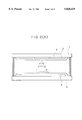
- FIG. 9 is a perspective view showing the external appearance of an electro-optical liquid crystal display in accordance with the present invention.
- FIGS. 10(A) to 10(D) and FIGS. 11(A) to 11(D) are cross sectional views and plan views showing a method of manufacturing an electro-optical liquid crystal display in accordance with the present invention.
- FIGS. 12(A) to 12(D) are cross sectional views showing a method of manufacturing an electro-optical liquid crystal display in accordance with the fourth embodiment of the present invention.
- FIGS. 13(A) to 13(C) are plan views showing a method of manufacturing an electro-optical liquid crystal display in accordance with the fifth embodiment of the present invention.
- FIGS. 14(A) and 14(B) are a cross sectional view and a plan view showing an electro-optical liquid crystal display which can be manufactured without opening contact holes.
- FIG. 2(A) A twisted nematic liquid crystal device in accordance with the present invention is schematically illustrated in FIG. 2(A), a glass substrate 1 is provided with an electrode arrangement 2 made of indium tin oxide.
- the electrode arrangement 2 comprises a number of electrode pads arranged in a matrix and defining pixels of the display.
- the inner surface of the substrate 1 is coated with polyimide film 3 over the first electrode arrangement 2.
- An orientation control surface is formed by rubbing the polyimide film 3.
- Another glass substrate 4 is prepared in the same manner but with an opposed electrode 5 which is common to the respective pixels. These substrates 1 and 4 are joined in order that the rubbing directions are perpendicular to each other.
- the liquid crystal molecules are aligned parallel to the rubbing directions at the both surfaces of the substrates so that a helix is formed between the substrates with a minimal energy condition of the liquid crystal molecule to modulate an incident light passing through the liquid crystal layer. If the electrode pads 2 of selected pixels are supplied with a driving voltage, in electric field is formed between the opposed electrode and each electrode pad so that the molecules of the liquid crystal are aligned normal to the substrates to pass an incident light without modulation.
- the present invention relates particularly to a technique to the circuit for supplying the driving voltage to each pixel.
- the details of the circuit will be described hereinafter in details.
- FIG. 2(B) is a schematic circuit diagram showing one pixel of the liquid crystal display.
- FIG. 2(C) is a graphical diagram showing voltage levels appearing at respective nodes of the circuit diagram during operation.
- the display comprises a number of such pixels arranged in a matrix. A particular column can be made active by activating a corresponding one of the data lines V D whereas a particular row can be made active by suitably activating the corresponding addressing line V G and the corresponding voltage supplying line V LC .
- the circuit for driving one pixel as shown in FIG. 2(B) comprises a first n type thin film transistor Tr 1 and a second n type thin film transistor Tr 2 .
- the first transistor Tr 1 is connected with the data line V D at its drain, the addressing line V G at its Sate and the gate of the second transistor Tr 2 at its source in order to transfer a level at the data line V D to the gate of the second transistor Tr 2 when addressed by the addressing line V G .
- the source and the drain of the second transistor Tr 2 are connected to the electrode pad of s liquid crystal LC and the voltage supplying line V LC .
- the electrode pad is formed to define one pixel in the liquid crystal.
- the circuit operates as follows. When addressed (given a positive gate signal from the addressing line V G ), the first transistor Tr 1 is turned on to transfer the data level at the data line V D to the gate of the second transistor Tr 2 . If the data level is "1", the second transistor Tr 2 is turned on to supply the pixel with a voltage at the voltage supplying line V LC in order to activate the pixel. On the other hand, if the data level is "0", the second transistor Tr 2 is turned off. The voltage at the gate of the second transistor Tr 2 is maintained when the addressing voltage is removed from the addressing line V G to address a next row.
- FIG. 2(C) illustrates signal levels at respective nodes and the relationship among these signals.
- the voltage supplying line V LC is alternatively set at a positive level and a negative level. Each signal is maintained for most of one frame except for a certain time period around the pulse appearing at the addressing line V G .
- the activated pixel is supplied with the positive or negative voltage from the voltage supplying line V LC for most of the frame length so that, even if current leakage occurs, the voltage shall not be decreased as long as the transistor Tr 2 is turned on during frames.
- FIG. 2(C) is detailedly explained also in SUMMARY OF THE INVENTION.
- each pair of adjacent pixels in a same column are formed to share a same voltage supplying line V LC .
- Other elements are constructed in the same manner as those of the first embodiment. By employing such a configuration, the density of horizontal lines is reduced by 25%. In the same manner, three or more pixels on a same column can share a common voltage supplying line by modifying the circuit design.
- one voltage supplying line supplies a driving voltage for two rows
- the driving voltage has to be grounded, when the two rows are addressed, in order to discharge electric charge accumulated in these pixels.
- an addressing signal is given to the addressing line V G with the data line V D being 1 so that the first and second transistors Tr 1 and Tr 2 are turned on.
- the addressing signal is removed from the addressing line V G and, instead, given to the next addressing line V G , so that the first transistor Tr 1 is turned off and the next first transistor Tr 1 , is turned on.
- the second transistor Tr 2 is then maintained turned on for the frame in order to transmit the voltage level from the voltage supplying line to the pixel.
- the corresponding second transistor Tr 2' is not turned an because the data line is set at 0 in this time and therefore maintained turned off for the frame after the first transistor tr 1' is turned off so that the voltage level V 2' at the lower pixel is maintained at 0.
- the data line is set at 1 when the addressing line V G' is addressed so that the first transistor Tr 1' is turned on and transmit 1 to the gate of the second transistor Tr 2' .
- the gate of the second transistor Tr 2' may be elevated only to a low voltage level as illustrated with broken line in the figure, The second transistor Tr 2' however, can be turned on, as long as the voltage level V 1' reaches to the threshold voltage of the second transistor, and therefore the voltage level V 2' can be elevated to the level of the voltage supplying line as illustrated with broken line.
- the operations of the first transistor and the second transistor will be analyzed below with reference to FIGS. 4(A) to 4(C).
- the parasitic capacitance C 1 between the source and the gate of the transistor Tr 1 and the parasitic capacitance C 2 between the drain and the gate of the transistor Tr 2 are illustrated in FIG. 4(A) with broken line. Because of the capacitance C 1 the voltage drop at the source of the first transistor Tr 1 is caused as explained before.
- the voltage drop ⁇ V is calculated by the following equation.
- the capacitance C 2 in dictated by the area of the gate electrode and the thickness and the dielectric constant, of the gate insulating film or the second transistor Tr 2 .
- the configuration of the transistor Tr 2 is designed in order that the capacitance C 2 is relatively small, e.g. no larger than 1% of the capacitance associated with the pixel. With this configuration, the display can be driven 100 times as faster as conventional displays.
- the capacitance C 1 can sometimes not be neglected as compared with the capacitance C 2 .
- the capacitance C 1 may be equal to the capacitance C 2 .
- the transistor addressed by the addressing line has a capacitance which is always smaller than that of the pixel at least by one order of magnitude, so that the voltage drop is not so large. If the capacitance C 1 equals the capacitance C 2 , the voltage drop is half the voltage applied to the gate of the first transistor Tr 1 .
- FIG. 4(B) illustrates the variation of the source level in response to the pulse application to the gate of the first transistor Tr 1 .
- the addressing signal is assumed to be 30 V.
- the data signal is assumed to be 20 V.
- the source level of the transistor Tr 1 then rises to 20 V (V 3 ) in response to the pulse of 30 V at the gate.
- the source level drops down to 5 V (V 4 ) after the gate voltage is removed because of a voltage drop equivalent to half the gate voltage, 30 V.
- Such situation is not fatal to the display in accordance with the present invention as long as 5 V is sufficient to turn off the second transistor Tr 2 .
- the second transistors can be equally turned on, unlike conventional displays whose quality reflects the disparity of the characteristics of the transistors.
- the high voltage is not directly applied to the liquid crystal so that the liquid crystal is not damaged by the high voltage.
- the high voltage is applied to the gate electrode of the second transistor Tr 2 which has a withstanding voltage from several times to ten and several times as high as that of the liquid crystal.
- the high voltage such as 30 V is not desirable from the view point of power consumption and damage to other circuitry or a human body,
- This problem can be solved by inverting the driving voltage supplied from the voltage supplying line as will be explained with FIG. 4(C). Namely, if the data signal supplied from the data line V D is negative, the absolute value of the voltage at the source is increased by the voltage drop as illustrated in FIG. 4(C).
- the driving voltage and the data signal are +5 V and -5 V, the final voltage of the source of the first transistor becomes -7.5 V.
- data may be supplied from the data line in terms of binary states corresponding to the source level of the first transistor.
- the second transistor therefore has to be selectively turned on or off in response to the negative voltage and the ground.
- the second transistor may be a p-channel enhancement mode transistor or an n-channel depression mode transistor.
- the source of the first transistor Tr 1 is pushed down to -2.5 V due to the voltage drop.
- the p-type second transistor may be turned on in error and transmit the driving voltage to the pixel, if it is a polysilicon transistor having a threshold voltage higher than -2.5 V.
- Such a trouble can be avoided by supplying a positive voltage such as +2.5 V to the data line to guarantee that the second transistor is turned off with its gate being at 0 V.
- the data is supplied in this case to the data line in terms or binary signals consisting of +2.5 V and -5 V.
- electric charge is eliminated from each pixel by grounding the voltage supplying line just before the corresponding first transistor is turned on.
- the electric charge can be more positively eliminated as in a third embodiment of the present invention illustrated in FIG. 5(A).
- a third transistor Tr 3 is connected between the addressing line and the voltage supplying line. Since the gate of the third transistor Tr 3 is connected to the data line, electric charge is eliminated during application of an addressing signal to the transistor Tr 3 .
- the parasitic capacitance between the gate and the drain of the third transistor Tr 3 causes a voltage drop. The voltage drop is neglected because the capacitance associated with the electrode pad or the pixel is substantially greater than the parasitic capacitance.
- a resistance may be inserted in parallel to the liquid crystal as illustrated in FIG. 6(B).
- Each pixel comprises a capacitor comprising the electrode pad, the electro-optical modulating layer (liquid crystal layer) and the opposed electrode arrangement.
- a resistor may be provided in parallel with the capacitor for each pixel.
- the time constant of the resistance and the liquid crystal is preferably selected to be on the same order as the time period of one frame, e.g. 33 milliseconds in usual mode displays. If more high speed discharge is desired as in digital grading, the time constant is selected to be as short as 500 microseconds for 64 grades or 125 microseconds for 256 grades in order to obtain clear images without afterimages and blurs.
- FIG. 5(A) illustrates one pixel of a liquid crystal display in accordance with a fourth embodiment of the present invention.
- the pixel is provided with an enhancement type NMOS transistor as the first transistor Tr 1 and a depression type NMOS transistor as the second transistor Tr 2 .
- the pixel is driven in the following manner as explained with reference to FIG. 5(B).
- the pixel is addressed by a pulse of 10 V supplied from the addressing line. Data is given to the data line in terms of binary signals of +8 V and -8 V.
- the first transistor is turned on and thereafter turned off to generate the source voltage V 1 which rises and then drops as illustrated and explained before.
- the source voltage V 1 rises to +8 V and drops to 3 V due to a voltage drop of 6 V.
- the transistor Tr 2 is turned on by the voltage V 1 and transmits the driving voltage from the voltage supplying line to the pixel, since it operates in a depression mode. If the data signal at the data line is -5 V in the next frame as illustrated, the source voltage V 1 is eventually set at -13 V due to a voltage drop of 3 V.
- the second transistor is turned off in response to the voltage change at the source and isolates the pixel from the voltage supplying line. Of course, it the data line remains at +8 V also in the next frame as depicted with broken line in the figure, the second transistor remains turned on to transmit the negative voltage at the voltage supplying line to the pixel.
- FIG. 7(A) illustrates one pixel or a liquid crystal display in accordance with a fifth embodiment of the present invention.
- the pixel is provided with CMOS transistors comprising an n-type transistor as the first transistor Tr 1 and a p-type transistor as the second transistor Tr 2 .
- the pixel is driven in the following manner as explained with reference to FIG. 7(B).
- the pixel is addressed by a pulse of 10 V supplied from the addressing line. Data is given to the data line in terms of binary signals of +8 V and -8 V. In this case, however, an negative voltage (-8 V) is given to the data line in order to activate the pixel in the opposite manner as compared to the previous embodiment.
- CMOS transistors comprising an n-type transistor as the first transistor Tr 1 and a p-type transistor as the second transistor Tr 2 .
- the pixel is driven in the following manner as explained with reference to FIG. 7(B).
- the pixel is addressed by a pulse of 10 V supplied from the addressing line
- the first transistor Tr 1 When a 10 V pulse is applied to the addressing line with the data line being set at +8 V, the first transistor Tr 1 is turned on and thereafter turned off to generate the source voltage V 1 which rises and then drops as illustrated and explained before. In this case, the source voltage V 1 rises to +8 V and drops to 3 V due to a voltage drop of 5 V.
- the transistor Tr 2 is turned off by the voltage V 1 and isolates the pixel from the voltage supplying line so that the pixel remains grounded. It the data signal at the data line is -8 V, after discharge of the pixel with the voltage supplying line being grounded, in the next frame as illustrated, the source voltage V 1 is eventually set at -13 V due to a voltage drop of 5 V.
- the second transistor is turned on in response to the voltage change at the gate and transmits the negative driving voltage from the voltage supplying line to the pixel.
- the second transistor remains turned on through the two frames to transmit the positive voltage and the negative voltage from the voltage supplying line to the pixel.
- FIG. 8 illustrates signals appearing within one frame which is divided into five periods.
- the shortest period lasts for a unit time To as shown in the right of the figure.
- the driving voltage is applied to the supplying line, e.g. for only 70% to 90% of the period for the above explained reason.
- the other tour periods are illustrated to have the same width as the shortest period in the figure for convenience, these periods last respectively for 16To, 2To, 8To and 4To in fact. All the rows of the display are scanned one time within each period in the same manner.
- the second transistor Tr 2 when an addressing signal having 1 microsecond pulse width is supplied to the addressing line V G of the row connected to the pixel with the corresponding data line V D being at +8 V, the second transistor Tr 2 is turned off and the off-condition is maintained throughout the shortest period.
- an addressing signal is supplied again to the addressing line V G at the start of the next 16To period with the corresponding data line V D being at +8 V, the off-condition of the second transistor is furthermore maintained throughout the 16To period. The voltage across the liquid crystal is 0 during these periods.
- the second transistor Tr 2 is turned on and the on-condition is maintained throughout the period.
- the on-condition of the second transistor is furthermore maintained throughout the 5To period.
- the liquid crystal is supplied with the driving voltage during these periods.
- an addressing signal is supplied again to the addressing line V G at the start of the next 4To period with the corresponding data line V D being at +8 V
- the second transistor Tr 2 is turned off and the off-condition of the second transistor is maintained throughout the 4To period.
- the liquid crystal is activated for total time of 10To out of 31To. It will be understood that the total time can be arbitrarily changed by the unit time To from 0 to 31To in order to obtain a desired grade by suitably combining the five periods.
- the unit period To is selected to be about a 32nd of one frame (33/32 milliseconds), i.e. about 1 millisecond.
- a space duration is provided between the addressing signal and the driving voltage.
- the space duration is selected to be 10 microseconds as shown in FIG. 8.
- the driving voltage lasts for 0.98 millisecond within the To period.
- the space duration has to be selected in proportion to the length or each period in order to obtain these grades in the ratios of whole numbers.
- the 16To period is provided with a space duration of 160 microseconds to have the driving voltage lasting for 15.68 milliseconds, which is exactly 16 times 0.98 millisecond.
- the space duration may be selected commonly to be 10 microseconds for all the periods since anyway the space duration is very short as compared with these periods. For example, if the 16To period is provided with a space duration of 10 microseconds to have the driving voltage lasting for 15.98 milliseconds, the ratio is 1:15,12 which is not so largely different from 1:16.
- the pulse width of the addressing signal is determined in accordance with the number of rows. If the number is 480, the pulse width is calculated by To/480, i.e. about 2 microseconds. In the figure, the pulse width is selected to be 1 microsecond for the purpose of avoiding interference between adjacent pulses. This requires high speed operations as compared with conventional cases of 30 to 70 microseconds pulse width. In accordance with the present invention, however, there arise no problem, since the load of the transistor is significantly light as compared with that in the conventional cases. Experiments were conducted utilizing low quality transistors. The voltage drop was 25% of the gate voltage. The source voltage of the first transistor is reduced to 90% of the initial level after time To and to 50% after time 16To. The display, however, normally operated as illustrated in FIG. 8.
- the peripheral circuit for driving the liquid crystal panel in accordance with the present invention has to supply suitable signals to the voltage supplying lines in addition to the addressing lines and the data lines. If the panel is formed with polysilicon semiconductor thin film transistors in a self-alignment manner, the peripheral circuit can be formed at the same time in order that particular care need not be taken for coupling the circuit with the matrix of the panel. If the transistors are polysilicon transistors formed in a non-self-alignment manner or amorphous silicon transistors, the peripheral circuit must he separately formed in driver ICs and externally connected to the respective terminals of the panel.
- a liquid crystal panel 901 is provided with the terminals of the addressing line in the left side of the panel and the terminals of the voltage supplying lines in the right side of the panel as illustrated in FIG. 9.
- Driving ICs for supplying addressing signals and driving ICs for supplying driving voltages are mounted respectively in the left side of the panel and the right side of the panel.
- the panel is divided into two portions as defined by broken line in the figure.
- the two portions comprises an upper panel and a lower panel which can be driven independently by data signals supplied from ICs mounted on both the upper and lower sides of the panel.
- the upper and lower panels can be scanned in parallel so that the driving frequency can be reduced by half. This is particularly advantageous if a higher grading is desired.
- FIG. 10(A) to 10(D) showing cross sectional views of the circuit in respective steps and FIGS. 11(A) to 11(D) showing corresponding plan views.
- numeral 107 designate the first transistor which has been discussed above in details while numeral 108 designate the second transistor.
- a blocking film 102 is formed on a glass substrate 101.
- the blocking film 102 is made of silicon nitride, aluminum oxide or the like which can block movable ions such as sodium ions occurring in the substrate from entering silicon semiconductor films 104 of 20 to 100 nm thickness which are formed on the blocking film 102 through an insulating film 103.
- the insulating film 103 is formed from silicon oxide and functions to hinder formation of interfacial states which could otherwise occur between the blocking film 102 and the semiconductor film 104.
- Each of the semiconductor films is formed with drain, source and channel regions therein.
- the left film becomes the active region of the first thin film transistor while the right film becomes the active region of the second thin film transistor.
- the conductivity types and the other characteristics of the respective semiconductor regions are determined in accordance with the whole circuit design which will be fully understood from the previous embodiments and therefore dispensed with here.
- the substrate 101 is then coated with an insulating film 105 of 50 to 200 nm thickness functioning as a gate insulating film over the semiconductor film 104.
- the gate insulating film is formed from silicon oxide, for example, by sputtering or ESR-CVD.
- Gate electrodes 106 are made, for example, of a highly doped polysilicon or a refractory metal such as Cr, W, which are particularly suitable when formed in a self-alignment manner, as illustrated in FIG. 10(A) and FIG. 11(A).
- a wiring 108 and a data line 110 are formed from a metal by etching in order to make contact with the source region 103 and the drain region 104 respectively.
- the wiring 109 is formed also to make contact with the gate electrode 106 of the second transistor 108 in order to connect the source of the first transistor to the gate electrode to the second transistor as illustrated in FIG. 11(B).
- the structure is then coated with an interlayer insulating film 111.
- an addressing line 113 and a voltage supplying line 112 are formed from a metal film by etching.
- the addressing line 113 and the voltage supplying line 112 are connected through the contact holes to the gate electrode or the first transistor 107 and the drain of the second transistor 108 respectively as illustrated in FIGS. 10(C) and 11(C).
- the interlayer insulating film 111 is particularly desired to be highly insulating because electric charge must be maintained at the gate of the second transistor during one frame.
- the upper surface of the structure is then coated with a surface smoothing film 114.
- a suitable contact hole is opened through the smoothing film 114 at the source of the second transistor 108, an electrode pad 115 of the pixel is formed from, a transparent conductive film such as an 1To (an alloy of indium oxide and tin oxide) film to make contact with the source of the second transistor 108.
- a transparent conductive film such as an 1To (an alloy of indium oxide and tin oxide) film to make contact with the source of the second transistor 108.
- FIGS. 12(A) to 12(D) a methods of producing the circuit for supplying driving voltages to the pixel of the liquid crystal display in accordance with the fourth embodiment of the present invention illustrated in FIG. 6(A) will be explained.
- numerals 209 and 210 designate the first and second transistors respectively in an inversed staggered type.
- FIGS. 12(A) to 12(D) are cross sectional views showing the circuit in respective steps.
- a blocking film 202 is formed on a glass substrate 201 in the same manner as in the previous method.
- the blocking film 102 is made of silicon nitride for blocking movable ions such as sodium ions.
- Gate electrodes 203 are formed on the blocking film 102.
- the gate electrode of the first transistor 210 is formed integrally with the addressing line. These gate electrodes are preferably made of a metal such as aluminum or a semiconductor such as silicon. When formed from aluminum, the yield can be improved by employing a low temperature process. Oxide films of 10 to 30 nm thickness may be formed on the external surfaces of the gate electrodes if desired, for example, by anodic oxidation or another suitable method.
- An interlayer insulating film 204 is coated on the substrate. The insulating film 204 overlies the gate electrode to function as the gate insulating films of the first and second transistors 209 and 210.
- An intrinsic amorphous silicon semiconductor film 205 is formed over the gate electrode of the first transistor 209 to form active region.
- an n + type microcrystalline silicon semiconductor film which is divided into source and drain regions 205 and 207 with an etching stopper 208 in between.
- an n type semiconductor amorphous silicon semiconductor film 206 is formed over the gate electrode to form active region, followed by forming on the semiconductor film 206 an n + type microcrystalline silicon semiconductor film which is divided into source and drain regions with an etching stopper in the same manner.
- the first transistor is formed as an enhancement device and the second transistor as a depression device as shown in FIG. 12(A).
- a data line 211 and an wiring 212 are formed from a metal.
- the data line 211 is patterned to make contact with the drain region 207 of the first transistor 209 and the wiring 212 is patterned to connect the source region 206 of the first transistor 209 and the gate electrode of the second transistor 210 in the same manner as illustrated in FIG. 11(B).
- the structure is then coated with an interlayer insulating film 213.
- a voltage supplying line 214 are formed from a metal film by etching.
- the voltage supplying line 214 are connected through the contact hole to the drain of the second transistor 210 as illustrated in FIG. 12(C).
- the upper surface of the structure is then coated with a surface smoothing film 216.
- an electrode pad 217 of the pixel is formed from a transparent conductive film such as an 1To film to make contact with the source of the second transistor 210 as illustrated in FIG. 12(D).
- the fifth embodiment of the present invention shown in FIG. 7(A) can be formed in the same manner as illustrated in FIGS. 12(A) to 12(D).
- the source and drain regions of the second semiconductor are formed from a p + type semiconductor. Since the mobility in a p + type amorphous semiconductor is vary low, the transistors are desirably formed from a polysilicon semiconductor. Laser annealing is suitable for producing the polysilicon semiconductor at low temperatures because when aluminum is used to form the gate electrodes it tends to be degraded at temperatures no lower than 550.
- FIGS. 13(A) to 13(C) shows plan views of the circuit for supplying driving voltages in accordance with the fifth embodiment of the present invention in respective production steps.
- a gate electrode 301 and a wiring 301' are patterned on a blocking film formed on a glass substrate in the same manner.
- the blocking film is made of silicon nitride for blocking movable ions such as sodium ions.
- the gate electrode 301 is formed to extend as an addressing line.
- These gate electrodes are preferably made of a metal such as aluminum or a semiconductor such as silicon. Oxide films of 10 to 30 nm thickness may be formed on the external surfaces of the gate electrodes if desired, for example, by anodic oxidation or another suitable method.
- an intrinsic amorphous silicon semiconductor film 302 is formed and patterned to cover both the gate electrodes of the first and second transistor to form active regions.
- a contact hole 304 is opened through the insulating film.
- an n + type microcrystalline silicon semiconductor film 306 which is patterned into source and drain regions with an etching stopper (not shown).
- the source region 305 is connected to the gate electrode 301' of the second transistor through the contact hole 304.
- CMOS devices comprising the first transistor and the second transistor as shown in FIG. 13(A) in completed.
- a data line 211 is formed from a metal in order to make contact with the drain 305 of the first transistor.
- An interlayer insulating film is then formed over the structure and contact holes 307 and 309 are craned therethrough to provide accesses to the source and the drain of the second transistor.
- a voltage supplying line 308 is formed to make contact with the source of the second transistor.
- An electrode pad 310 of the pixel is formed to make contact with the drain or the second transistor.
- FIGS. 14(A) and 14(B) are a cross sectional view and a plan view showing the configuration of a device in accordance with the present invention which can be manufactured without opening contact holes.
- An addressing line 402 is formed on a glass substrate 401.
- the addressing line functions as the gate electrode of the first transistor.
- the surface of the addressing line may be oxidized to form an oxide film, of 10 to 200 nm thickness for example by anoding.
- An interlayer insulating film 403 is coated on the substrate over the addressing line and etched back to provide a flat upper surface.
- the interlayer insulating film 403 functions as the gate insulating film above the addressing line 402.
- the side surfaces of the addressing line may be tapered to avoid formation of sharp edges and improve the adhessivity to the interlayer insulating film 403. By this tapering, the upper width of the addressing line 402 is narrowed so that the channel length of the first transistor is decreased. This is advantageous because a lower resistance of the addressing line and a shorter channel length are always desired.
- a semiconductor film 405 of 20 to 100 nm is formed to provide the active region of the first transistor.
- the film 405 is made of a polycrystalline silicon, an amorphous silicon or another silicon semiconductor of an intermediate crystalline state between them.
- a silicon nitride film is formed on the semiconductor film 405 and patterned as a channel stopper 406 to define a channel region in the underlying semiconductor film 405, The channel stopper 406 is particularly effective when the semiconductor film 405 is very thin and therefore tends to be easily damaged,
- an n + type microcrystalline silicon semiconductor film is formed over the structure and patterned in order to provide a first pattern 407 extending as the gate electrode of the second transistor and as the source of the first transistor located over the right sides of the semiconductor film 405 and the stopper 406 as illustrated in FIG. 14(B) and a second pattern 408 extending over the lift sides of the semiconductor film 405 and the stopper 406 as the drain of the second transistor.
- a data line 409 is formed from a metallic material in order to make contact with the second pattern 408.
- a semiconductor film 411 of 20 to 100 nm is formed to provide the active region of the second transistor.
- the film 411 is made of a polycrystalline silicon, an amorphous silicon or another silicon semiconductor of an intermediate crystalline state between them.
- a silicon nitride film is formed on the semiconductor film 411 and patterned as a channel stopper 412 to define a channel region in the underlying semiconductor film 411.
- a p + type microcrystalline silicon semiconductor film is formed over the structure and patterned in order to provide the source and the drain of the second transistor to provide a CMOS structure.
- a voltage supplying line 414 is formed to make contact with the source of the second transistor.
- An electrode pad 415 of the pixel is formed to make contact with the drain of the second transistor.
Abstract
An electro-optical liquid crystal display suitable for displaying highly graded images. A plurality of pixels are arranged in a matrix and supplied with data signals through data lines extending in the column direction. Extending in the row direction are a plurality of addressing lines and a plurality of voltage signal lines. Each row is selected by activating by each of the addressing lines and supplied with a driving voltage from each of the voltage supplying lines.
Description
This application is a continuation of Ser. No. 07/959,918, filed Oct. 14, 1992, now abandoned.
1. Field of the Invention
The present invention relates in general to an electro-optical liquid crystal display suitable for finely graded operation and methods of driving and manufacturing the same.
2. Description of the Prior Art
Recently, thin film transistor liquid crystal displays (TFTLCD for short) have been increasingly broadly utilized, along with the development of color liquid crystal displays, rather than simple matrix type liquid crystal displays because the former type is particularly excellent in terms of brightness, contrast and wide view angles.
FIG. 1(A) is a circuit diagram showing a driving circuit for controlling one pixel of such a TFTLCD. As shown in the figure, a single thin film transistor is provided for the pixel located at each intersection of a matrix diagonal wiring comprising horizontal addressing lines (only one line VG being illustrated) and vertical data lines (also only one line VD being illustrated). The drain (D) of the transistor is connected to the corresponding one of the data lines while the source (S) thereof is connected to the corresponding one of the electrode pads defining pixels of the display (not shown). The gate of the transistor is connected to the corresponding one of the addressing lines VG. Such a matrix type design has been broadly employed already in the DRAM technique so that the reliability thereof is believed to have been fully established. In the case of the driving technique for liquid crystal display, however, there remain still several problems to be solved since the operation of liquid crystal displays includes also analog data manipulation.
FIG. 1(B) is a schematic diagram showing examples of signals applied to the addressing line VG and the data line VD and the resultant driving voltage at the electrode of the corresponding pixel in response to the signals. If a liquid crystal material is subjected to a DC voltage for a substantial time period, the characteristics of the materials are degraded. The signal at the data line therefore is periodically inverted (usually for each frame) in order to invert the direction of the voltage applied across the liquid crystal material.
The mechanism of the operation of the pixel is next explained. When a voltage pulse is applied to the gate, the transistor is turned on in order to transmit electric charge to the electrode pad of the pixel from the data line being at a high level so that the voltage level of the electrode pad is increased (region t1). The increase, however, is not so fast. In the case the transistor is made of an amorphous silicon semiconductor, the mobility of carriers is so low that the pulse applied to the gate is sometimes removed and the transistor is turned off before the voltage at the pixel reaches to the necessary level. In the case that the transistor is made of polysilicon, such undesirable situation is substantially improved, if the operational speed is so high that the pulse width is narrower than one microseconds, however, even the polysilicon transistor can no longer follow such a high speed. It takes 30 milliseconds in usual cases to scan one frame. The pulse width of the addressing signal is therefore about 50 microseconds In the case that the number of the addressing lines is 480 (480 rows display). If higher definition of grading is desired, however, the pulse width narrower than one microsecond becomes necessary.
The voltage at the pixel then drops by V. This drop, called "rebound", is caused by charge accumulated in the parasitic capacitance which is formed by the overlap between the gate electrode and the source region. The voltage drop increases as the parasitic capacitance increases. In the case of displays utilizing amorphous TFTS, a capacitance is provided across the liquid crystal at the pixel in order to reduce the voltage drop. The provision of such a particular capacitance, in turn, increases the load of the TFT and the other peripheral circuit and decreases the aperture ratio because of the wiring for the capacitances so that the brightness is decreased.
In the case of polysilicon transistors, such a problem of the voltage drop is not so significant since the self-alignment process can be employed for forming the gate electrode and the source and drain regions. The voltage drop, however, still exists as high as one volts which may become a substantial problem in future when a higher definition is required.
The voltage at the pixel gradually decreases until a next addressing line arrives (region t2) because of discharge due mainly to leakage current passing through the transistor being turned off. The next pulse is than applied to the addressing line VG. Since the voltage level of the pulse is inverted in this time, the voltage level at the pixel is also gradually decreased to the inverted level in the same manner as described above.
When the addressing pulse is removed from the addressing line, the absolute value or the voltage at the pixel is increased in this case by the voltage drop V followed by gradually decrease due to discharge. As understood from the illustration, the voltage applied to the pixel is asymmetrical resulting in several problems such as flicker or deterioration of the liquid crystal material.
Furthermore, it is to be noted that the voltage at the pixel having a waveform, of such a complicated pattern substantially tends to vary from pixel to pixel. For example, the rise of the voltage at the pixel in region t1 depends upon the several parameters of the transistor, e.g. the mobility, the channel length, the thickness of the active region, the gate voltage (the voltage applied to the addressing line) and the drain voltage (the voltage applied to the data line). The mobility of the transistor depends largely upon the manufacturing process so that pixel to pixel variation will not be so large. when the panel size becomes large in future, however, it will be the case that the variation within the same panel can not be neglected. Variation in the thickness of the active region may be also a problem in the case of large panels. Variations in the channel length and the channel width are usually as large as about 10% of more from pixels near the driver to pixels apart from the driver.
The voltage drop depends upon the parasitic capacitance of the TFT. The dispersion of the capacitance is about 20% in the case of non-self alignment processes and about 10% in the case of self-alignment processes. Furthermore, since the voltage drop is in proportion to the gate voltage applied, the dispersion of the parasitic capacitance and the dispersion of the gate voltage form a multiplier action to widen the dispersion of the voltage drop.
On the other hand, the gradually decrease of the voltage at the pixel depends largely upon the channel length, the channel width, the characteristics of the active region, of the transistor (TFT). As a result, the voltage level at the pixel fluctuates from solid line to broken line in FIG. 1(B). Particularly accurate duality control is required in manufacturing processes for the devices in order that the dispersion of the voltage at the pixel is always within a tolerable range. As a result, the yield is significantly decreased. It may be impossible to meet future requirements for highly-value-added products with a high yield whereas low quality products may be manufactured with a relatively high yield.
At the present time, a plurality of grades in brightness can be constructed by controlling the voltages at the signals lines. The manufacture of the graded displays seems to be almost impossible even with 16 grades in accordance with the current technique from the view point as discussed below. The threshold voltages of usual twisted nematic liquid crystals are 5 V or therearound, which are divided by 16 into 30 mV for realizing 16 grades. Considering dispersion in the voltage rise at time t1, in the voltage drop and in the discharge, as above discussed, the dispersion of the voltage at the pixel would easily exceed 300 mV unless products are carefully sifted out.
From the above view point, the inventors have advocated digital graded displaying systems in place of analog grading systems. The digital grading are realized by controlling the time for which the liquid crystal is subjected to a driving voltage at each pixel. Details are described in Japanese Patent Applications Nos. Hei3-169305, 169306, 169307 and 209869 of the same applicant. The frequencies required for driving the digital grading displays, however, are 20 to 300 times as high as conventional frequencies so that TFTs of CMOS structure have to be arranged at each pixel in place of NMOSTFT alone. It is also difficult even with such digital systems to suppress disturbance at grading due to dispersion of the characteristics of the TFTs.
For example, when an intermediate grade is selected by limiting the voltage application time only to 45% of one frame, 110% of the predetermined voltage level may be applied to certain pixels whereas 90% of the level may be applied to other pixels, in which case the display incurs 20% or wider dispersion of the driving voltage since 1.1×45%=49.59% in the former pixels and 0.9×45%=40.5% in the later pixels. In this case, only 8 grade seems to be possible.
In order to solve this problem, as described in Japanese Patent Application No. Hei3-209870, the inventors proposed for the driving device to collect information about characteristics of respective pixels and input the information into an external memory device. The input data signal are processed in advance on the basis of the information and outputted to the respective pixels in order to make correction. The data processing, however, is so complicated that peripheral circuits must carry heavy burdens. Furthermore, it takes a substantial time to examine the respective pixels and input correction data, For example, if the examination and the data inputs for one pixel takes one second, the total time of 85 hours is necessary in the case of a panel having 640×480 pixels resulting in a significantly increased cost.
It is an object of the present invention to provide an electro-optical device (liquid crystal display) suitable for digital grading.
It is another object of the present invention to provide a method of driving an electro-optical device (liquid crystal display) suitable for digital grading.
It is a further object or the present invention to provide a method of manufacturing an electro-optical device (liquid crystal display) with a high yield.
Additional objects, advantages and novel features of the present invention will be sat forth in the description which follows and in part will become apparent to those skilled in the art upon examination of the following or may be learned by practice of the present invention. The object and advantages of the invention may be realized and attained by means of the instrumentalities and combinations particularly pointed out in the appended claims.
To achieve the foregoing and other object, and in accordance with the present invention, as embodied and broadly described herein, in an electro-optical liquid crystal display having a first substrate on which a plurality of electrode pads are formed in order to define a plurality of pixels arranged in a matrix, a second substrate on which an opposed electrode arrangement is formed, an electro-optical modulating layer (liquid crystal layer) disposed between the first and second substrates, and a control circuit for supplying driving voltages to the electrode pads respectively, the control circuit comprises a plurality of addressing lines tar scanning the pixels by sequentially supplying an addressing signal to the pixels arranged in each row or matrix to be addressed, a plurality of data lines for supplying data to the pixels arranged in the row addressed by the addressing signal, a plurality of voltage supplying lines for supplying a driving signal to the pixels arranged in the row addressed by the addressing signal and means for selectively connecting or disconnecting the electrode pad of each pixel with a corresponding one of the voltage supplying line in accordance with data supplied from the data lines when that pixel is addressed by the addressing signal. Particularly, the means comprises a plurality of second transistors provided respectively for the plurality of the pixels, each second transistor being connected between a corresponding one of the electrode pads and a corresponding one of the voltage supplying lines and a plurality of first transistors provided for the plurality of the pixels respectively, each first transistor being connected between the gate of a corresponding one of said second transistors and a corresponding one of said data lines, the gate of said first transistor being connected to a corresponding one of said addressing line.
The electro-optical liquid crystal display in accordance with the present invention is particularly suitable for displaying finely graded images. The plurality of pixels are arranged in a matrix and supplied with data signals through the data lines extending in the column direction. Extending in the row direction are a plurality of the addressing lines and a plurality of the voltage signal lines. Each row is selected by activating each of the addressing lines and supplied with a driving voltage from each of the voltage supplying lines.
Referring now to FIGS. 2(B) and 2(C), a typical example of a circuit for controlling each pixel of the liquid crystal display in accordance with the present invention will be briefly explained. FIG. 2(B) is a schematic circuit diagram showing one pixel of the liquid crystal display. FIG. 2(C) is a graphical diagram, showing voltage levels appearing at respective nodes of the circuit diagram during operation. The display comprises a number of such pixels arranged in a matrix. A particular column can be made active by activating a corresponding one of the data lines VD whereas a particular row can be made active by suitably activating the corresponding addressing line VG and then the corresponding voltage supplying line VLC.
The circuit for driving one pixel as shown in FIG. 2(B) comprises a first n type thin film transistor Tr1 and a second n type thin film transistor Tr2. The first transistor Tr1 is connected with the data line VD at its drain, the addressing line VD at its gate and the gate of the second transistor Tr2 at its source in order to transfer a voltage level at the data line VD to the gate of the second transistor Tr2 when addressed by the addressing line VG. The source and the drain of the second transistor Tr2 are connected to the electrode pad of a liquid crystal LC and the voltage supplying line VLC. The electrode pad is formed to define one pixel in the liquid crystal.
The circuit operates as follows. When addressed (given a positive gate signal from he addressing line VG), the first transistor Tr1 is turned on to transfer the data level at the data line VD to the gate of the second transistor Tr2. If the data level is "1", the second transistor Tr2 is turned on to supply the pixel with a voltage at the voltage supplying line VLC in order to activate the pixel. On the other hand, if the data level is "0", the second transistor Tr2 is turned off. The voltage at the gate of the second transistor Tr2 is maintained when the addressing voltage is removed from the addressing line VG to address subsequent rows.
In accordance with the above structure, the signal level at the respective data line is not directly transmitted to the pixel so that the timing of the signal operation is significantly relaxed. Namely, even if the voltage level at the respective data line deviates from the predetermined level, the pixel is supplied with a constant driving voltage as long as the deviating level can turn on the second transistor Tr2.
Namely, as discussed above, the pulse width of the addressing signal is extremely short, e.g. 70 microseconds for typical cases, or from shorter than tenth to several-hundredth that of the typical cases for digital grading. The voltage level supplied to the respective pixel tends to fluctuate because of such a short operating time.
On the other hand, it is understood from analysis of the operation of the display in accordance with the present invention that even if the pulse width or an addressing signal applied to the first transistor Tr1 is also very short resulting in variation of the resultant source voltage level, the source voltage is not directly transferred to the pixel but, applied to the gate of the second transistor Tr2 instead and therefore is enough as long as its lowest level can control the operation of the second transistor Tr2.
If such conditions are satisfied, a constant voltage can be supplied to the respective pixels from the voltage supplying lines by controlling the on/off operation of the second transistors. Accordingly, the voltage supplied to each pixel is not dictated by the signals from the data lines. The signals from the data lines only determine the on/off condition of the second transistors.
Furthermore, it should be noted that the switching speed of the second transistors may be substantially lower than that of the first transistors. The second transistor can perform its task even if it operates after completion of the on/off operation of the first transistor since electric charge is trapped at the gate of the second transistor Tr2 after operation of the first transistor. Accordingly, the second transistor can be an amorphous silicon semiconductors TFT having a slow switching speed even for digital grading with 32 grades.
Furthermore, the load upon the first transistor of FIG. 2(B) is significantly reduced as compared with that in conventional configurations. Prior to the present invention, electric charge must pass through the transistor addressed within a time shorter than 70 microseconds to the pixel. Electric charge passing through the first transistor of the present invention is accumulated in the capacitance formed between the gate and the drain of the second transistor Tr2. For example, the capacitance associated with each pixel is 30 times as large as that of the capacitance formed between the gate and the drain of the second transistor Tr2 in the case that the area and the thickness of the electrode pad of each pixel are 300 micrometers×300 micrometers and 2 micrometers respectively and the area and the thickness of the gate insulating film of the second transistor are 10 micrometers×10 micrometers and 0.2 micrometers. The ratio between these capacitances is furthermore increased to 120 if the area of the gate electrode is decreased to 5 micrometers×6 micrometers.
It will be apparently understood that heavy loads are carried on the transistors in conventional cases. On the other hand, in accordance with the present invention, the load is decreased by a factor of 30 to 120 or more. This means that the switching speed of the first transistor can be substantially increased to 30 to 120 times that in the conventional cases in which digital grading can not be realized with amorphous transistor whose mobility is very low.
The electric charge to be passed through the first transistor, however, is significantly small in accordance with the present invention so that the above problem is not the case. Accordingly, it is possible to drive amorphous silicon TFTs even to realize 64 or more grades. Amorphous silicon TFTs can be produced at relatively low temperatures as compared with polysilicon TFTs so that massproduction is facilitated to obtain a high yield and reduce the production cost.
The second transistor, on the other hand, can sufficiently perform its task if its switching speed is no lower than one hundredth, preferably no lower than twentieth, that of the first transistor. The amount of electric charge passing through the second transistor is substantially equal to that in conventional cases. Since the switching speed required of the second transistor is very low, however, amorphous silicon TFTs can be employed for digital grading with 33 grades. The switching speed or amorphous silicon TFTS is usually about 70 microseconds which is only 7% of the minimum cycle of the 32 grade digital grading, i.e. 33/32 milliseconds (about 1 millisecond), so that such higher grading can be realized with no problem.
The channel width can be increased for the purpose of increasing the driving capability of the transistor Tr2. care must be paid in this case because the capacitance between the gate and the drain of the second transistor Tr2 is also increased resulting in a heavy load on the first transistor Tr1. For example, if the channel width is increased by a factor of 5 to obtain 5 times the driving capability, the load on the first transistor Tr1 is also increased by a factor of 5 so that the effective switching speed of the first transistor Tr1 is reduced to 20%.
Referring to FIG. 2(C), a method of driving the liquid crystal display as illustrated in FIG. 2(B) will be described. The addressing line VG and the data line VD are supplied with similar signals as in a conventional display. The signal supplied through the data line, however, is a pure digital 0 or 1 which simply turns off or on the second transistor Tr2. The voltage source line (voltage supplying line) VLC is supplied alternately with a positive signal or a negative signal in synchronism with the addressing signal on the corresponding addressing line VG. The signal on the voltage supplying line however, is set at 0 during the time when the addressing line is supplied with an addressing pulse. Reference letters VG to V2 in FIG. 2(C) correspond to similar letters written in FIG. 2(B).
The voltage levels at respective nodes change during operation as follows. The voltage v1 at the source of the first transistor Tr1 (i.e. at the gate of the second transistor Tr2) rises as solid line, then lightly drops responsive to disappearing of the addressing signal and gradually decreases due to discharge through the transistor Tr 1.
On the other hand, the voltage level at the source of the second transistor Tr2 (i.e. at the electrode pad of the pixel) changes as follows. First, the second transistor Tr2 is turned on since the source of the first transistor Tr1 rises. Next, since a driving voltage is supplied to the voltage supplying line, the electrode pad is charged to a predetermined level. In this connection, it is noted that since the second transistor Tr2 is already tuned on when the driving voltage is supplied, the charging time is dictated by the on resistance of the transistor Tr2 and the capacitance associated with the electrode pad, resulting in a rapid onset.
The driving voltage is supplied to the voltage supplying line only when a certain time elapses after the addressing signal disappears. Of course, it is also possible to supply the driving voltage just after the addressing signal disappears. When finely grading is performed by means of high speed TFTs as the second transistor Tr2 in accordance with the digital control technique, particularly such a technique as described in Japanese Patent Application Nos. Hei3-163870 to 163873, however, the later alternative timing is not an good.
For example, consider a digital grading with 84 grades. The minimum periodic cycle of the addressing signals is 500 microseconds. Although the pulse width of the addressing signal is about 1 microsecond in the case of a matrix having 480 rows, the first transistor Tr1 can perform its task because of the light load thereon as explained above. There arise no problems even if the source of the transistor Tr1 rises not so much, as long as the second transistor can be driven. Accordingly, the source of the first transistor Tr1 is considered to sufficiently rise to drive the second transistor Tr2.
In the case that the second transistor Tr2 is designed only to have a switching speed of 70 microseconds, there are formed a number of such transistors with in an actual panel and some transistors among them may have switching speeds as high as 50 microseconds. Such disparity of switching speed originates from production variation such as differences in mobility due to slightly differences in quality or the active region, differences in channel length and channel width due to slight variation of photomasks. In this case, if the driving voltage is supplied to the voltage supplying line just after the addressing signal, some transistor Tr2 having 70 microsecond switching speed is turned on 10 microsecond after other transistor Tr2 on the same panel having 60 microsecond switching speed is turned on. The difference of 10 microseconds is equal to 2% of the periodic cycle of the addressing signal.
The problematic 2% dispersion makes the 64 grades meaningless because the time dispersion of voltage application to the pixels must be limited to 1.6% in order to actually realize 64 grades. Of course, the problematic dispersion can be suppressed by sifting out productions resulting in a high cost to make even the switching speeds. The production cost, however, is significantly increased.
On the other hand, if the driving voltage is supplied to the voltage supplying line when a certain time (80 or 100 microseconds) elapses after the addressing pulse disappears, all the pixels are given the driving voltage substantially at the same time point in each cycle. In this case, the problematic dispersion is dictated only by factors such as the on resistance of the transistor Tr2 and the capacitance associated with the electrode pad. The on resistance and the capacitance are of the order of 1016 ohm and the order of 10-13 F so that the time constant is about 100 nanoseconds.
Accordingly, even if the time constant is dispersed from pixel to pixel, the problematic dispersion is no larger than 100 nanoseconds unless the dispersion of the time constant does not exceed 50%. 100 nanoseconds is extremely small as compared with the periodic cycle of 500 microseconds (0.02%) and meets the requirement of within 1.8%. Accordingly, it is effective for finely grading to supply the driving voltage a certain time after the addressing signal disappears.
Similar attention has to be paid when the driving voltage is removed. Namely, a certain time period defining a space duration is provided between the removal of the driving voltage and the application of the addressing signal in order to discharge electric charge accumulated in the electrode pad of the pixel. If the driving voltage is supplied to the electrode pad when the addressing voltage is supplied to the sate of the first transistor Tr1, the electric charge remains at the electrode pad in the case that the data signal on the data line VD is 0 and turns off the second transistor Tr2. In order to avoid such a case, electric charge accumulated at the electrode pad is discharged for the certain time period u interposed between the driving voltage signal and the addressing signal. The certain time period T corresponds to the time constant as discussed above.
In the next cycle, the driving voltage is inverted. The negative driving voltage is supplied to the drain of the second transistor Tr2 also the certain time period after the addressing signal. The data signal need not be inverted unlike in conventional displays.
As seen from FIG. 2(C), voltage drops are observed only in the gate voltage of the second transistor Tr2. The driving voltage applied to the electrode pad of the pixel exhibits no such variation and no reduction due to natural discharge. This is because the driving voltage is continuously given from the voltage supplying line in accordance with the present invention whereas the voltage at the pixel is supported by electric charge locked by a transistor being turned off in conventional cases. The present invention just features this difference.
Furthermore, broken line is plotted in the figure for the purpose of showing possible poor characteristics of a first transistor Tr1. Namely, because of the poor characteristics, the source voltage can not reach to the drain voltage and is largely influenced by voltage drop when the addressing voltage disappears, followed by a relatively large natural discharge. In accordance with a conventional display having such a transistor, displayed images comprise irregular colors so that the display is not accepted. As seen from the figure, however, the pixel driven by such a transistor can operate with no trouble. Namely, even if the transistor Tr1 exhibits such poor characteristics as shown by broken line, there arise no problem as long as the source voltage can drive the second transistor Tr2.
As seen from the figure, oven if the source voltage V1 is lowered as plotted with broken line, no influence appears on the driving voltage at the electrode pad of the pixel. The voltage at the data line is preferably selected in order to guarantee that a most poor one of the first transistors can drive the corresponding second transistor. Of course, the voltage must not be selected to destroy the transistor.
In accordance with experiments conducted by the applicants using small scale liquid crystal panels with 100 pixels (10 rows×10 columns), it was very easy to form nine for each ten transistors, functioning as the first transistor Tr1, capable of providing 5 V or higher voltage at its source during operation of the panel in the case that the addressing voltage and the voltage at the data line corresponding to 1 are 15 V and 10 V respectively. The yield was no lower than 95%. In this case, when the voltages applied to the gate and the drain of the first transistor were furthermore increased by 5 V respectively, the yield of the transistors providing 5 V or higher was 99% without no destructed sample.
Experiments were conducted for reference by constructing a conventional type liquid crystal display with transistors having such poor characteristics. As a result, only 60% of transistors could provide voltages at corresponding electrode pads within a range of ±0.9 V from the average voltage of 7.2 V. This means that 40% of the transistors were inappropriate even for realizing only 8 grades. When panels were selected in order that at least 90% of transistors met the requirement of 7.2 ±0.9 V, the yield was significantly decrease or course, such experiments were not conducted at best conditions so that it may be possible to improve the result to some extent. The production of more large panel liquid crystal displays, however, is considered to be very difficult.
From the conventional view point, such a configuration having two transistors for one pixel might seem to have adverse affects for increasing the yield. The requirement upon the characteristics of the transistors, however, is significantly low so that the yield is not reduced by the configuration.
The present invention is therefore based upon the concept that if a certain pixel is selected to be active, a constant voltage should be always applied to that pixel. Accordingly, it is avoided that the voltage level at the pixel gradually decreases due to discharge. In accordance with the present invention, the yield is significantly improved as compared with those of conventional analog or digital systems. The displays in accordance with the present invention can maintain a sufficient grading ability even with TFTs having poor characteristics, and as a result the yield and cost performance are significantly improved. It is also advantageous to manufacture displays having qualities no lower than those of conventional displays only with a lower manufacturing cost.
If TFTs are formed by self-alignment processes in the manufacturing method of the present invention, the liquid crystal displays as manufactured become furthermore excellent in operation at high frequencies and in realizing finely graded images. Even if polysilicon TFTs are formed by non-self-alignment processes in the manufacturing method of the present invention, it is possible to display clear images in 64 or more grades without particular difficulties at a cost which is no higher than or significantly lower than that of conventional analog systems capable of 16 graded images. Also even if amorphous silicon TFTs are formed by non-self-alignment processes in the manufacturing method of the present invention, it is possible to display clear images in 15 or more grades at a low cost.
The accompanying drawings, which are incorporated in and form a part of the invention and, together with the description, serve to explain the principles of the invention.
FIGS. 1(A) and 1(B) are a schematic circuit diagram and a graphical diagram showing a prior art electro-optical liquid crystal display.
FIG. 2(A) is a cross sectional view showing a general configuration of an electro-optical liquid crystal display in accordance with the present invention.
FIGS. 2(B) and 2(C) are a schematic circuit diagram and a graphical diagram showing an electro-optical liquid crystal display and its operation in accordance with a first embodiment of the present invention.
FIGS. 3(A) and 3(B) are a schematic circuit diagram and a graphical diagram showing an electro-optical liquid crystal display and its operation in accordance with a second embodiment of the present invention.
FIGS. 4(A) to 4(C) are a schematic circuit diagram and graphical diagrams for explaining in details the operation of the electro-optical liquid crystal display in accordance with the first embodiment of the present invention.
FIG. 5(A) is a schematic circuit diagram showing an electro-optical liquid crystal display in accordance with a third embodiment of the present invention.
FIG. 5(B) is a schematic circuit diagram showing an electro-optical liquid crystal display in accordance with a modification of the third embodiment of the present invention.
FIGS. 6(A) and 6(B) are a schematic circuit diagram and a graphical diagram showing an electro-optical liquid crystal display and its operation in accordance with a fourth embodiment of the present invention.
FIGS. 7(A) and 7(B) are a schematic circuit diagram and a graphical diagram showing an electro-optical liquid crystal display and its operation in accordance with a fifth embodiment of the present invention.
FIG. 8 is a schematic diagram showing a grading operation of an electro-optical liquid crystal display in accordance with the present invention.
FIG. 9 is a perspective view showing the external appearance of an electro-optical liquid crystal display in accordance with the present invention.
FIGS. 10(A) to 10(D) and FIGS. 11(A) to 11(D) are cross sectional views and plan views showing a method of manufacturing an electro-optical liquid crystal display in accordance with the present invention.
FIGS. 12(A) to 12(D) are cross sectional views showing a method of manufacturing an electro-optical liquid crystal display in accordance with the fourth embodiment of the present invention.
FIGS. 13(A) to 13(C) are plan views showing a method of manufacturing an electro-optical liquid crystal display in accordance with the fifth embodiment of the present invention.
FIGS. 14(A) and 14(B) are a cross sectional view and a plan view showing an electro-optical liquid crystal display which can be manufactured without opening contact holes.
A twisted nematic liquid crystal device in accordance with the present invention is schematically illustrated in FIG. 2(A), a glass substrate 1 is provided with an electrode arrangement 2 made of indium tin oxide. The electrode arrangement 2 comprises a number of electrode pads arranged in a matrix and defining pixels of the display. The inner surface of the substrate 1 is coated with polyimide film 3 over the first electrode arrangement 2. An orientation control surface is formed by rubbing the polyimide film 3. Another glass substrate 4 is prepared in the same manner but with an opposed electrode 5 which is common to the respective pixels. These substrates 1 and 4 are joined in order that the rubbing directions are perpendicular to each other. When a twisted nematic liquid crystal material is disposed between the first and second substrates, the liquid crystal molecules are aligned parallel to the rubbing directions at the both surfaces of the substrates so that a helix is formed between the substrates with a minimal energy condition of the liquid crystal molecule to modulate an incident light passing through the liquid crystal layer. If the electrode pads 2 of selected pixels are supplied with a driving voltage, in electric field is formed between the opposed electrode and each electrode pad so that the molecules of the liquid crystal are aligned normal to the substrates to pass an incident light without modulation.
The present invention relates particularly to a technique to the circuit for supplying the driving voltage to each pixel. The details of the circuit will be described hereinafter in details.
Referring now to FIGS. 2(B) and 2(C), a liquid crystal display in accordance with a first embodiment of the present invention will be explained. FIG. 2(B) is a schematic circuit diagram showing one pixel of the liquid crystal display. FIG. 2(C) is a graphical diagram showing voltage levels appearing at respective nodes of the circuit diagram during operation. The display comprises a number of such pixels arranged in a matrix. A particular column can be made active by activating a corresponding one of the data lines VD whereas a particular row can be made active by suitably activating the corresponding addressing line VG and the corresponding voltage supplying line VLC.
The circuit for driving one pixel as shown in FIG. 2(B) comprises a first n type thin film transistor Tr1 and a second n type thin film transistor Tr2. The first transistor Tr1 is connected with the data line VD at its drain, the addressing line VG at its Sate and the gate of the second transistor Tr2 at its source in order to transfer a level at the data line VD to the gate of the second transistor Tr2 when addressed by the addressing line VG. The source and the drain of the second transistor Tr2 are connected to the electrode pad of s liquid crystal LC and the voltage supplying line VLC. The electrode pad is formed to define one pixel in the liquid crystal.
The circuit operates as follows. When addressed (given a positive gate signal from the addressing line VG), the first transistor Tr1 is turned on to transfer the data level at the data line VD to the gate of the second transistor Tr2. If the data level is "1", the second transistor Tr2 is turned on to supply the pixel with a voltage at the voltage supplying line VLC in order to activate the pixel. On the other hand, if the data level is "0", the second transistor Tr2 is turned off. The voltage at the gate of the second transistor Tr2 is maintained when the addressing voltage is removed from the addressing line VG to address a next row.
FIG. 2(C) illustrates signal levels at respective nodes and the relationship among these signals. As shown in the figure, the voltage supplying line VLC is alternatively set at a positive level and a negative level. Each signal is maintained for most of one frame except for a certain time period around the pulse appearing at the addressing line VG. The pixel is reset at 0 during the certain time period with VLC =0 when the pixel is addressed by the addressing line VG. In this regard, therefore, it is noted that the activated pixel is supplied with the positive or negative voltage from the voltage supplying line VLC for most of the frame length so that, even if current leakage occurs, the voltage shall not be decreased as long as the transistor Tr2 is turned on during frames. FIG. 2(C) is detailedly explained also in SUMMARY OF THE INVENTION.
In the configuration illustrated in FIG. 2(B), two signals line VG and VLC have to be formed for one row and therefore such a configuration seems to decrease the aperture ratio of pixels. In the configuration of conventional displays utilizing amorphous silicon TFTS, the similar problem is also the case since an additional line is formed in parallel to an addressing line in order to form a supplemental capacitance to cope with a parasitic capacitance associated with the TFT.
This problem is solved by employing the circuit shown in FIG. 3(A) illustrating a second embodiment of the present invention. In this circuit, each pair of adjacent pixels in a same column are formed to share a same voltage supplying line VLC. Other elements are constructed in the same manner as those of the first embodiment. By employing such a configuration, the density of horizontal lines is reduced by 25%. In the same manner, three or more pixels on a same column can share a common voltage supplying line by modifying the circuit design.
In this case, since one voltage supplying line supplies a driving voltage for two rows, the driving voltage has to be grounded, when the two rows are addressed, in order to discharge electric charge accumulated in these pixels. Namely, there is a space duration at the voltage supplying line VLC corresponding to the addressing pulses to the addressing lines VG and VG'.
In FIG. 3(B), an addressing signal is given to the addressing line VG with the data line VD being 1 so that the first and second transistors Tr1 and Tr2 are turned on. Next, the addressing signal is removed from the addressing line VG and, instead, given to the next addressing line VG, so that the first transistor Tr1 is turned off and the next first transistor Tr1, is turned on. The second transistor Tr2 is then maintained turned on for the frame in order to transmit the voltage level from the voltage supplying line to the pixel. Although the first transistor Tr1' is turned on, the corresponding second transistor Tr2' is not turned an because the data line is set at 0 in this time and therefore maintained turned off for the frame after the first transistor tr1' is turned off so that the voltage level V2' at the lower pixel is maintained at 0.
In the next frame, the data line is set at 1 when the addressing line VG' is addressed so that the first transistor Tr1' is turned on and transmit 1 to the gate of the second transistor Tr2'. If the characteristics of the transistor Tr1' are not good, the gate of the second transistor Tr2' may be elevated only to a low voltage level as illustrated with broken line in the figure, The second transistor Tr2' however, can be turned on, as long as the voltage level V1' reaches to the threshold voltage of the second transistor, and therefore the voltage level V2' can be elevated to the level of the voltage supplying line as illustrated with broken line.
The operations of the first transistor and the second transistor will be analyzed below with reference to FIGS. 4(A) to 4(C). The parasitic capacitance C1 between the source and the gate of the transistor Tr1 and the parasitic capacitance C2 between the drain and the gate of the transistor Tr2 are illustrated in FIG. 4(A) with broken line. Because of the capacitance C1 the voltage drop at the source of the first transistor Tr1 is caused as explained before. The voltage drop ΔV is calculated by the following equation.
ΔV=C.sub.1 V.sub.G /(C.sub.1 +C.sub.2)
The capacitance C2 in dictated by the area of the gate electrode and the thickness and the dielectric constant, of the gate insulating film or the second transistor Tr2. In accordance with the present invention, the configuration of the transistor Tr2 is designed in order that the capacitance C2 is relatively small, e.g. no larger than 1% of the capacitance associated with the pixel. With this configuration, the display can be driven 100 times as faster as conventional displays.
In this case, however, the capacitance C1 can sometimes not be neglected as compared with the capacitance C2. For example, the capacitance C1 may be equal to the capacitance C2. In a conventional display, the transistor addressed by the addressing line has a capacitance which is always smaller than that of the pixel at least by one order of magnitude, so that the voltage drop is not so large. If the capacitance C1 equals the capacitance C2, the voltage drop is half the voltage applied to the gate of the first transistor Tr1. FIG. 4(B) illustrates the variation of the source level in response to the pulse application to the gate of the first transistor Tr1. The addressing signal is assumed to be 30 V. The data signal is assumed to be 20 V. The source level of the transistor Tr1 then rises to 20 V (V3) in response to the pulse of 30 V at the gate. The source level, however, drops down to 5 V (V4) after the gate voltage is removed because of a voltage drop equivalent to half the gate voltage, 30 V. Such situation is not fatal to the display in accordance with the present invention as long as 5 V is sufficient to turn off the second transistor Tr2. Namely, irrespective of the variation of the source levels of the first transistors in the pixels of a panel, the second transistors can be equally turned on, unlike conventional displays whose quality reflects the disparity of the characteristics of the transistors. Furthermore, even if the data signal or the present invention is increased to a high voltage level to cope with the worst transistor, the high voltage is not directly applied to the liquid crystal so that the liquid crystal is not damaged by the high voltage. Namely, in this case, the high voltage is applied to the gate electrode of the second transistor Tr2 which has a withstanding voltage from several times to ten and several times as high as that of the liquid crystal.
On the other hand, the high voltage such as 30 V is not desirable from the view point of power consumption and damage to other circuitry or a human body, This problem can be solved by inverting the driving voltage supplied from the voltage supplying line as will be explained with FIG. 4(C). Namely, if the data signal supplied from the data line VD is negative, the absolute value of the voltage at the source is increased by the voltage drop as illustrated in FIG. 4(C). When the driving voltage and the data signal are +5 V and -5 V, the final voltage of the source of the first transistor becomes -7.5 V. In this case, data may be supplied from the data line in terms of binary states corresponding to the source level of the first transistor. The second transistor therefore has to be selectively turned on or off in response to the negative voltage and the ground. For example, the second transistor may be a p-channel enhancement mode transistor or an n-channel depression mode transistor. Anyway, it is an advantage that both the addressing line and the data line can be driven by a single voltage source of 5 V.
When the addressing line is addressed with the data line being 0, the source of the first transistor Tr1 is pushed down to -2.5 V due to the voltage drop. In this case, the p-type second transistor may be turned on in error and transmit the driving voltage to the pixel, if it is a polysilicon transistor having a threshold voltage higher than -2.5 V. Such a trouble can be avoided by supplying a positive voltage such as +2.5 V to the data line to guarantee that the second transistor is turned off with its gate being at 0 V. The data is supplied in this case to the data line in terms or binary signals consisting of +2.5 V and -5 V.
In the preceding embodiments, electric charge is eliminated from each pixel by grounding the voltage supplying line just before the corresponding first transistor is turned on. The electric charge can be more positively eliminated as in a third embodiment of the present invention illustrated in FIG. 5(A). In this case, a third transistor Tr3 is connected between the addressing line and the voltage supplying line. Since the gate of the third transistor Tr3 is connected to the data line, electric charge is eliminated during application of an addressing signal to the transistor Tr3. The parasitic capacitance between the gate and the drain of the third transistor Tr3 causes a voltage drop. The voltage drop is neglected because the capacitance associated with the electrode pad or the pixel is substantially greater than the parasitic capacitance. Alternatively, a resistance may be inserted in parallel to the liquid crystal as illustrated in FIG. 6(B). Each pixel comprises a capacitor comprising the electrode pad, the electro-optical modulating layer (liquid crystal layer) and the opposed electrode arrangement. A resistor may be provided in parallel with the capacitor for each pixel. The time constant of the resistance and the liquid crystal is preferably selected to be on the same order as the time period of one frame, e.g. 33 milliseconds in usual mode displays. If more high speed discharge is desired as in digital grading, the time constant is selected to be as short as 500 microseconds for 64 grades or 125 microseconds for 256 grades in order to obtain clear images without afterimages and blurs.
It is impossible in conventional displays to provide such a bypass resistance through which electric charge escapes. Since dispersion of such resistances is usually about 20% or higher, the voltages across the liquid crystal at respective pixels are dispersed during one frame also in a 20% span. In accordance with the present invention, however, the voltage across the liquid crystal is supplied from the voltage supplying line and therefore the supplied voltages are maintained for each frame.
FIG. 5(A) illustrates one pixel of a liquid crystal display in accordance with a fourth embodiment of the present invention. The pixel is provided with an enhancement type NMOS transistor as the first transistor Tr1 and a depression type NMOS transistor as the second transistor Tr2. The pixel is driven in the following manner as explained with reference to FIG. 5(B). The pixel is addressed by a pulse of 10 V supplied from the addressing line. Data is given to the data line in terms of binary signals of +8 V and -8 V. When a 10 V pulse is applied to the addressing line with the data line being set at +8 V, the first transistor is turned on and thereafter turned off to generate the source voltage V1 which rises and then drops as illustrated and explained before. In this case, the source voltage V1 rises to +8 V and drops to 3 V due to a voltage drop of 6 V. The transistor Tr2 is turned on by the voltage V1 and transmits the driving voltage from the voltage supplying line to the pixel, since it operates in a depression mode. If the data signal at the data line is -5 V in the next frame as illustrated, the source voltage V1 is eventually set at -13 V due to a voltage drop of 3 V. The second transistor is turned off in response to the voltage change at the source and isolates the pixel from the voltage supplying line. Of course, it the data line remains at +8 V also in the next frame as depicted with broken line in the figure, the second transistor remains turned on to transmit the negative voltage at the voltage supplying line to the pixel.
FIG. 7(A) illustrates one pixel or a liquid crystal display in accordance with a fifth embodiment of the present invention. The pixel is provided with CMOS transistors comprising an n-type transistor as the first transistor Tr1 and a p-type transistor as the second transistor Tr2. The pixel is driven in the following manner as explained with reference to FIG. 7(B). The pixel is addressed by a pulse of 10 V supplied from the addressing line. Data is given to the data line in terms of binary signals of +8 V and -8 V. In this case, however, an negative voltage (-8 V) is given to the data line in order to activate the pixel in the opposite manner as compared to the previous embodiment. When a 10 V pulse is applied to the addressing line with the data line being set at +8 V, the first transistor Tr1 is turned on and thereafter turned off to generate the source voltage V1 which rises and then drops as illustrated and explained before. In this case, the source voltage V1 rises to +8 V and drops to 3 V due to a voltage drop of 5 V. The transistor Tr2 is turned off by the voltage V1 and isolates the pixel from the voltage supplying line so that the pixel remains grounded. It the data signal at the data line is -8 V, after discharge of the pixel with the voltage supplying line being grounded, in the next frame as illustrated, the source voltage V1 is eventually set at -13 V due to a voltage drop of 5 V. The second transistor is turned on in response to the voltage change at the gate and transmits the negative driving voltage from the voltage supplying line to the pixel. Of course, if the pixel is desired to be activated for the two frames as depicted with broken line in the figure, the second transistor remains turned on through the two frames to transmit the positive voltage and the negative voltage from the voltage supplying line to the pixel.
Next, examples of signals supplied to the respective lines of the liquid crystal display in accordance with the fifth embodiment of the present invention to construct images in 32 grades will be explained with reference to FIG 8. Of course, a greater number of grades than 32 can be realized in the same manner. Details of the technique is described in Japanese Patent Application No. Hei3-209859 filed by the same applicant.
It takes 33 microseconds to construct an image of one frame. FIG. 8 illustrates signals appearing within one frame which is divided into five periods. The shortest period lasts for a unit time To as shown in the right of the figure. The driving voltage is applied to the supplying line, e.g. for only 70% to 90% of the period for the above explained reason. Although the other tour periods are illustrated to have the same width as the shortest period in the figure for convenience, these periods last respectively for 16To, 2To, 8To and 4To in fact. All the rows of the display are scanned one time within each period in the same manner. For example, when an addressing signal having 1 microsecond pulse width is supplied to the addressing line VG of the row connected to the pixel with the corresponding data line VD being at +8 V, the second transistor Tr2 is turned off and the off-condition is maintained throughout the shortest period. When an addressing signal is supplied again to the addressing line VG at the start of the next 16To period with the corresponding data line VD being at +8 V, the off-condition of the second transistor is furthermore maintained throughout the 16To period. The voltage across the liquid crystal is 0 during these periods. When an addressing signal is supplied again to the addressing line VD at the start of the next 8To period with the corresponding data line VD being at -8 V, the second transistor Tr2 is turned on and the on-condition is maintained throughout the period. When an addressing signal is supplied again to the addressing line VG at the start of the next 8To period with the corresponding data line VD being at -8 V, the on-condition of the second transistor is furthermore maintained throughout the 5To period. The liquid crystal is supplied with the driving voltage during these periods. When an addressing signal is supplied again to the addressing line VG at the start of the next 4To period with the corresponding data line VD being at +8 V, the second transistor Tr2 is turned off and the off-condition of the second transistor is maintained throughout the 4To period. In this case, the liquid crystal is activated for total time of 10To out of 31To. It will be understood that the total time can be arbitrarily changed by the unit time To from 0 to 31To in order to obtain a desired grade by suitably combining the five periods.
The unit period To is selected to be about a 32nd of one frame (33/32 milliseconds), i.e. about 1 millisecond. As explained in the previous embodiment, a space duration is provided between the addressing signal and the driving voltage. The space duration is selected to be 10 microseconds as shown in FIG. 8. The driving voltage lasts for 0.98 millisecond within the To period. Exactly saying, the space duration has to be selected in proportion to the length or each period in order to obtain these grades in the ratios of whole numbers. For example, the 16To period is provided with a space duration of 160 microseconds to have the driving voltage lasting for 15.68 milliseconds, which is exactly 16 times 0.98 millisecond. The space duration, however, may be selected commonly to be 10 microseconds for all the periods since anyway the space duration is very short as compared with these periods. For example, if the 16To period is provided with a space duration of 10 microseconds to have the driving voltage lasting for 15.98 milliseconds, the ratio is 1:15,12 which is not so largely different from 1:16.
The pulse width of the addressing signal is determined in accordance with the number of rows. If the number is 480, the pulse width is calculated by To/480, i.e. about 2 microseconds. In the figure, the pulse width is selected to be 1 microsecond for the purpose of avoiding interference between adjacent pulses. This requires high speed operations as compared with conventional cases of 30 to 70 microseconds pulse width. In accordance with the present invention, however, there arise no problem, since the load of the transistor is significantly light as compared with that in the conventional cases. Experiments were conducted utilizing low quality transistors. The voltage drop was 25% of the gate voltage. The source voltage of the first transistor is reduced to 90% of the initial level after time To and to 50% after time 16To. The display, however, normally operated as illustrated in FIG. 8.
The peripheral circuit for driving the liquid crystal panel in accordance with the present invention has to supply suitable signals to the voltage supplying lines in addition to the addressing lines and the data lines. If the panel is formed with polysilicon semiconductor thin film transistors in a self-alignment manner, the peripheral circuit can be formed at the same time in order that particular care need not be taken for coupling the circuit with the matrix of the panel. If the transistors are polysilicon transistors formed in a non-self-alignment manner or amorphous silicon transistors, the peripheral circuit must he separately formed in driver ICs and externally connected to the respective terminals of the panel. When the panel is designed to operate in a very high grading mode such as 256 grades, even self-aligned polysilicon thin film transistors can not be used and particular external driver ICs must be provided instead. In such a case, a liquid crystal panel 901 is provided with the terminals of the addressing line in the left side of the panel and the terminals of the voltage supplying lines in the right side of the panel as illustrated in FIG. 9. Driving ICs for supplying addressing signals and driving ICs for supplying driving voltages are mounted respectively in the left side of the panel and the right side of the panel. The panel is divided into two portions as defined by broken line in the figure. The two portions comprises an upper panel and a lower panel which can be driven independently by data signals supplied from ICs mounted on both the upper and lower sides of the panel. In this fashion, the upper and lower panels can be scanned in parallel so that the driving frequency can be reduced by half. This is particularly advantageous if a higher grading is desired.
Next, several methods of producing the circuit for supplying driving voltages to the pixel of the liquid crystal display in accordance with the present invention will be explained. These method can be suitably carried out, with some modification if necessary, in order to construct a variety of circuits including the above discussed embodiments, e.g. driving circuits comprising PMOS TFTs, NMOS TFTs, depression mode MOS TFTs, enhancement mode MOSTFTs, planar type transistors, stagger type transistors, or other type transistors having impurity regions formed in a self-alignment manner or a non-self-alignment manner. A first example is described with reference to FIG. 10(A) to 10(D) showing cross sectional views of the circuit in respective steps and FIGS. 11(A) to 11(D) showing corresponding plan views. In the figure, numeral 107 designate the first transistor which has been discussed above in details while numeral 108 designate the second transistor.
A blocking film 102 is formed on a glass substrate 101. The blocking film 102 is made of silicon nitride, aluminum oxide or the like which can block movable ions such as sodium ions occurring in the substrate from entering silicon semiconductor films 104 of 20 to 100 nm thickness which are formed on the blocking film 102 through an insulating film 103. The insulating film 103 is formed from silicon oxide and functions to hinder formation of interfacial states which could otherwise occur between the blocking film 102 and the semiconductor film 104.
Each of the semiconductor films is formed with drain, source and channel regions therein. The left film becomes the active region of the first thin film transistor while the right film becomes the active region of the second thin film transistor. The conductivity types and the other characteristics of the respective semiconductor regions are determined in accordance with the whole circuit design which will be fully understood from the previous embodiments and therefore dispensed with here. The substrate 101 is then coated with an insulating film 105 of 50 to 200 nm thickness functioning as a gate insulating film over the semiconductor film 104. The gate insulating film is formed from silicon oxide, for example, by sputtering or ESR-CVD. Gate electrodes 106 are made, for example, of a highly doped polysilicon or a refractory metal such as Cr, W, which are particularly suitable when formed in a self-alignment manner, as illustrated in FIG. 10(A) and FIG. 11(A).
After suitable contact holes are opened through the insulating film 105 at the source 103 and the drain regions 104 of the first transistor 107, a wiring 108 and a data line 110 are formed from a metal by etching in order to make contact with the source region 103 and the drain region 104 respectively. The wiring 109 is formed also to make contact with the gate electrode 106 of the second transistor 108 in order to connect the source of the first transistor to the gate electrode to the second transistor as illustrated in FIG. 11(B).
The structure is then coated with an interlayer insulating film 111. After suitable contact holes are opened through the interlayer insulating film 111 at the gate electrode of the first transistor 107 and the drain of the second transistor 108, an addressing line 113 and a voltage supplying line 112 are formed from a metal film by etching. The addressing line 113 and the voltage supplying line 112 are connected through the contact holes to the gate electrode or the first transistor 107 and the drain of the second transistor 108 respectively as illustrated in FIGS. 10(C) and 11(C). The interlayer insulating film 111 is particularly desired to be highly insulating because electric charge must be maintained at the gate of the second transistor during one frame.
The upper surface of the structure is then coated with a surface smoothing film 114. After a suitable contact hole is opened through the smoothing film 114 at the source of the second transistor 108, an electrode pad 115 of the pixel is formed from, a transparent conductive film such as an 1To (an alloy of indium oxide and tin oxide) film to make contact with the source of the second transistor 108.
Referring next to FIGS. 12(A) to 12(D), a methods of producing the circuit for supplying driving voltages to the pixel of the liquid crystal display in accordance with the fourth embodiment of the present invention illustrated in FIG. 6(A) will be explained. In the figure, numerals 209 and 210 designate the first and second transistors respectively in an inversed staggered type. FIGS. 12(A) to 12(D) are cross sectional views showing the circuit in respective steps.
A blocking film 202 is formed on a glass substrate 201 in the same manner as in the previous method. The blocking film 102 is made of silicon nitride for blocking movable ions such as sodium ions. Gate electrodes 203 are formed on the blocking film 102. The gate electrode of the first transistor 210 is formed integrally with the addressing line. These gate electrodes are preferably made of a metal such as aluminum or a semiconductor such as silicon. When formed from aluminum, the yield can be improved by employing a low temperature process. Oxide films of 10 to 30 nm thickness may be formed on the external surfaces of the gate electrodes if desired, for example, by anodic oxidation or another suitable method. An interlayer insulating film 204 is coated on the substrate. The insulating film 204 overlies the gate electrode to function as the gate insulating films of the first and second transistors 209 and 210.
An intrinsic amorphous silicon semiconductor film 205 is formed over the gate electrode of the first transistor 209 to form active region. On the intrinsic semiconductor film 205 is formed an n+ type microcrystalline silicon semiconductor film which is divided into source and drain regions 205 and 207 with an etching stopper 208 in between. For the second transistor 210, an n type semiconductor amorphous silicon semiconductor film 206 is formed over the gate electrode to form active region, followed by forming on the semiconductor film 206 an n+ type microcrystalline silicon semiconductor film which is divided into source and drain regions with an etching stopper in the same manner. AS a result, the first transistor is formed as an enhancement device and the second transistor as a depression device as shown in FIG. 12(A).
After forming a contact hole to provide an address to the gate electrode of the second transistor 210, a data line 211 and an wiring 212 are formed from a metal. The data line 211 is patterned to make contact with the drain region 207 of the first transistor 209 and the wiring 212 is patterned to connect the source region 206 of the first transistor 209 and the gate electrode of the second transistor 210 in the same manner as illustrated in FIG. 11(B).
The structure is then coated with an interlayer insulating film 213. After a suitable contact hole is opened through the interlayer insulating film 213 at the drain of the second transistor 210, a voltage supplying line 214 are formed from a metal film by etching. The voltage supplying line 214 are connected through the contact hole to the drain of the second transistor 210 as illustrated in FIG. 12(C). The upper surface of the structure is then coated with a surface smoothing film 216. After a suitable contact hole is opened through the smoothing film 210 at the source of the second transistor 210, an electrode pad 217 of the pixel is formed from a transparent conductive film such as an 1To film to make contact with the source of the second transistor 210 as illustrated in FIG. 12(D).
The fifth embodiment of the present invention shown in FIG. 7(A) can be formed in the same manner as illustrated in FIGS. 12(A) to 12(D). In this case, whereas both the active regions 205 and 206 are formed from an intrinsic semiconductor, the source and drain regions of the second semiconductor are formed from a p+ type semiconductor. Since the mobility in a p+ type amorphous semiconductor is vary low, the transistors are desirably formed from a polysilicon semiconductor. Laser annealing is suitable for producing the polysilicon semiconductor at low temperatures because when aluminum is used to form the gate electrodes it tends to be degraded at temperatures no lower than 550.
FIGS. 13(A) to 13(C) shows plan views of the circuit for supplying driving voltages in accordance with the fifth embodiment of the present invention in respective production steps.
A gate electrode 301 and a wiring 301' are patterned on a blocking film formed on a glass substrate in the same manner. The blocking film is made of silicon nitride for blocking movable ions such as sodium ions. The gate electrode 301 is formed to extend as an addressing line. These gate electrodes are preferably made of a metal such as aluminum or a semiconductor such as silicon. Oxide films of 10 to 30 nm thickness may be formed on the external surfaces of the gate electrodes if desired, for example, by anodic oxidation or another suitable method. After an interlayer insulating film is coated on the substrate as the gate insulating films of the first and second transistors, an intrinsic amorphous silicon semiconductor film 302 is formed and patterned to cover both the gate electrodes of the first and second transistor to form active regions. A contact hole 304 is opened through the insulating film. On the intrinsic semiconductor film 302 over the gate electrode of the first transistor is formed an n+ type microcrystalline silicon semiconductor film 306 which is patterned into source and drain regions with an etching stopper (not shown). The source region 305 is connected to the gate electrode 301' of the second transistor through the contact hole 304. For the second transistor, p+ type microcrystalline silicon semiconductor film 303 is formed on the intrinsic semiconductor film 303 and patterned into source and drain regions with an etching stopper in the same manner. As a result, CMOS devices comprising the first transistor and the second transistor as shown in FIG. 13(A) in completed.
A data line 211 is formed from a metal in order to make contact with the drain 305 of the first transistor. An interlayer insulating film is then formed over the structure and contact holes 307 and 309 are craned therethrough to provide accesses to the source and the drain of the second transistor. A voltage supplying line 308 is formed to make contact with the source of the second transistor. An electrode pad 310 of the pixel is formed to make contact with the drain or the second transistor.
This process can be applied for other embodiments of the present invention by suitably selecting the conductivity types of the respective semiconductors and taking necessary modification if necessary. The respective steps of the above process to form the CMOS devise are summarized as follows. The numbers in brackets ! are the mask number.
1) formation of the addressing line 301 and the gate electrode 301' 1!,
2) formation of the gate insulating film (interlayer insulating film),
3) formation of the semiconductor film 302 2!,
4) formation of the etching stoppers (not shown) 3!,
5) formation of the contact hole 304 4!,
6) formation of the semiconductor film 305 5!,
7) formation of the semiconductor film 303 6!,
8) formation of the data line 306 7!,
9) formation or the interlayer insulating film,
10) formation of the contact holes 307 and 309 8!,
11) formation of the voltage supplying line 308 9!,
12) formation of the electrode pad 310 of the pixel 10!.
FIGS. 14(A) and 14(B) are a cross sectional view and a plan view showing the configuration of a device in accordance with the present invention which can be manufactured without opening contact holes.
An addressing line 402 is formed on a glass substrate 401. The addressing line functions as the gate electrode of the first transistor. The surface of the addressing line may be oxidized to form an oxide film, of 10 to 200 nm thickness for example by anoding. An interlayer insulating film 403 is coated on the substrate over the addressing line and etched back to provide a flat upper surface. The interlayer insulating film 403 functions as the gate insulating film above the addressing line 402. The side surfaces of the addressing line may be tapered to avoid formation of sharp edges and improve the adhessivity to the interlayer insulating film 403. By this tapering, the upper width of the addressing line 402 is narrowed so that the channel length of the first transistor is decreased. This is advantageous because a lower resistance of the addressing line and a shorter channel length are always desired.
A semiconductor film 405 of 20 to 100 nm is formed to provide the active region of the first transistor. The film 405 is made of a polycrystalline silicon, an amorphous silicon or another silicon semiconductor of an intermediate crystalline state between them. A silicon nitride film is formed on the semiconductor film 405 and patterned as a channel stopper 406 to define a channel region in the underlying semiconductor film 405, The channel stopper 406 is particularly effective when the semiconductor film 405 is very thin and therefore tends to be easily damaged,
Next, an n+ type microcrystalline silicon semiconductor film is formed over the structure and patterned in order to provide a first pattern 407 extending as the gate electrode of the second transistor and as the source of the first transistor located over the right sides of the semiconductor film 405 and the stopper 406 as illustrated in FIG. 14(B) and a second pattern 408 extending over the lift sides of the semiconductor film 405 and the stopper 406 as the drain of the second transistor. In accordance with the present invention, since electric charge is accumulated in the source of the first transistor and the gate electrode of the second transistor, such an integrated structure of the source and the gate electrode is very advantageous. Then a data line 409 is formed from a metallic material in order to make contact with the second pattern 408.
After coating an interlayer insulating film 410 of silicon oxide over the structure, a semiconductor film 411 of 20 to 100 nm is formed to provide the active region of the second transistor. The film 411 is made of a polycrystalline silicon, an amorphous silicon or another silicon semiconductor of an intermediate crystalline state between them. A silicon nitride film is formed on the semiconductor film 411 and patterned as a channel stopper 412 to define a channel region in the underlying semiconductor film 411. Next, a p+ type microcrystalline silicon semiconductor film is formed over the structure and patterned in order to provide the source and the drain of the second transistor to provide a CMOS structure. A voltage supplying line 414 is formed to make contact with the source of the second transistor. An electrode pad 415 of the pixel is formed to make contact with the drain of the second transistor.
This process can be applied for other embodiments of the present invention by suitably selecting the conductivity types of the respective semiconductors and making necessary modification if necessary. The respective steps of the above process to form the CMOS device are summarized as follows. The numbers in brackets ! are the mask number.
1) formation of the addressing line 402 1!,
2) formation of the gate insulating film (interlayer insulating film) 403,
3) formation of the semiconductor film 405 2!,
4) formation of the etching stopper 406 3!,
5) formation of the semiconductor films 407 and 408 4!,
6) formation of the data line 409 5!,
7) formation of the gate insulating film (interlayer insulating film) 410;
8) formation of the semiconductor film 411 6!,
9) formation of the etching stopper 412 7!,
10) formation of the semiconductor film 413 8!,
11) formation of the voltage supplying line 414 9!,
12) formation of the electrode pad of the pixel 415 10!.
The foregoing description of preferred embodiments has been presented for purposes of illustration and description. It is not intended to be exhaustive or to limit the invention to the precise form described, and obviously many modifications and variations are possible in light of the above teaching. The embodiment was chosen in order to explain most clearly the principles of the invention and its practical application thereby to enable others in the art to utilize most effectively the invention in various embodiments and with various modifications as are suited to the particular use contemplated.
Claims (16)
1. An electro-optical device of an active matrix type comprising a plurality of addressing lines, a plurality of data lines, a plurality of voltage supply lines and a plurality of pixels, said addressing lines and said voltage supply lines being formed in parallel and each pixel being provided with PMOS and NMOS transistors, the gate of one of said transistors being connected to the source of the other transistor.
2. An electro-optical device of an active matrix type comprising a plurality of addressing lines, a plurality of data lines, a plurality of voltage supply lines and a plurality of pixels, said addressing lines and said voltage supply lines being formed in parallel and each pixel being provided with a MOS transistor formed in a self-alignment manner and a MOS transistor formed in a non-self-alignment manner.
3. In an electro-optical device comprising a first substrate on which a plurality of electrode pads are formed in order to define a plurality of pixels arranged in a matrix, a second substrate on which an opposed electrode arrangement is formed, an electro-optical modulating layer disposed between said first and second substrates, and a control circuit for supplying driving voltages to said electrode pads respectively, said control circuit comprising:
a plurality of addressing lines for scanning said pixels by sequentially supplying an addressing signal to the pixels arranged in each row of said matrix to be addressed;
a plurality of data lines for supplying data to the pixels arranged in the row addressed by said addressing-signal;
a plurality of voltage supplying lines for supplying a driving signal to the pixels arranged in the row addressed by said addressing signal; and
means for selectively connecting or disconnecting the electrode pad of each pixel with a corresponding one of said voltage supplying line in accordance with data supplied from said data lines when that pixel is addressed by the addressing signal,
wherein each of said pixels comprises a capacitor comprising the electrode pad, the electro-optical modulating layer and the opposed electrode arrangement, and said electro-optical device further comprises a resistor provided in parallel with said capacitor.
4. The electro-optical device as claimed in claim 3 wherein said means comprises:
a plurality of first transistors provided for said plurality of the pixels respectively, each first transistor being connected between a corresponding one of said electrode pads and a corresponding one of said voltage supplying lines; and
a plurality of second transistors provided for said plurality of the pixels respectively, each second transistor being connected between the gate of a corresponding one of said first transistors and a corresponding one of said data lines, the gate of said second transistor being connected to a corresponding one of said addressing lines.
5. The electro-optical device as claimed in claim 4 wherein each voltage supplying line supplies driving voltages to the pixels arranged on the two adjacent rows of said matrix.
6. The device of claim 4 wherein said first transistors are enhancement mode transistors and said second transistors are depletion mode transistors.
7. The device of claim 4 wherein said first transistors are PMOS transistors and said second transistors are NMOS transistors.
8. A method of driving an electro-optical device of an active matrix type comprising a plurality of voltage supplying lines, a plurality of addressing lines and a plurality of data lines, and said addressing lines and said voltage supplying lines are formed in parallel, wherein electric charge is discharged from a pixel electrode of said device when said voltage supplying lines are deactivated.
9. The method of claim 8 wherein said electric charge is charged in said pixel electrode before said discharging.
10. An electro-optical device of an active matrix type comprising:
a voltage supplying line;
a first transistor connected with said voltage supplying line at one of source and drain thereof;
a pixel electrode connected with said first transistor at the other of said source and drain;
a second transistor for supplying a gate signal to a gate of said first transistor;
an addressing line connected with said second transistor;
a data line connected with said second transistor; and
an opposed electrode,
wherein a capacitance between a gate electrode and a drain region of said second transistor is no larger than 1% of a capacitance between said pixel electrode and said opposed electrode.
11. An electro-optical device according to claim 10 wherein each of said first and second transistors is planar type or stagger type.
12. An electro-optical device of an active matrix type comprising:
a pixel electrode;
a first line;
a second line;
a voltage supplying line;
a first transistor connected with said first line and said second line at a gate thereof and one of source and drain thereof, respectively; and
a second transistor connected with the other of said source and drain at a gate of said second transistor, connected with said pixel electrode at one of source and drain of said second transistor for supplying a static voltage to said pixel electrode for a desired period of time, and connected with said voltage supplying line at the other of the source and drain of said second transistor,
wherein signals on said second line being selectively set at a positive voltage and a negative voltage in accordance with information to be displayed.
13. The electro-optical device of claim 12 wherein signals on said first line and signals on said voltage supplying line being given in synchronism with each other.
14. The electro-optical device of claim 12 wherein said electro-optical device comprises a plurality of pixels, each pixel being provided with an enhancement mode transistor and a depletion mode transistor.
15. An electro-optical device according to claim 12 wherein each of said first and second transistors is planar type or stagger type.
16. An active matrix electro-optical device comprising:
a first gate line and a second gate line extending in parallel;
a voltage supply line extending in parallel with and between said first and second gate lines;
a data line orthogonal to said first and second gate lines;
first and second pixel electrodes disposed between said voltage supply line and said first and second gate lines, respectively to form first and second pixels, each of said first and second pixels being provided with a first transistor and a second transistor, the first and second pixels being associated with the first and second gate lines, respectively,
the gate of each of said first transistors being connected to the corresponding one of the gate lines;
the drain (or source) of each of said first transistors being connected to the gate of the corresponding one of the second transistors;
the source (or drain) of each of said first transistors being commonly connected to said data line;
drain (or source) of each of the second transistors being connected to the corresponding one of the pixel electrodes; and
the source (or drain) of each of the second transistors being commonly connected to said voltage supply line.
Priority Applications (7)
| Application Number | Priority Date | Filing Date | Title |
|---|---|---|---|
| US08/419,956 US5828429A (en) | 1991-10-16 | 1995-04-10 | Electro-optical device and method of driving with voltage supply lines parallel to gate lines and two transistors per pixel |
| US08/978,597 US6023308A (en) | 1991-10-16 | 1997-11-26 | Active matrix device with two TFT's per pixel driven by a third TFT with a crystalline silicon channel |
| US09/342,236 US7116302B2 (en) | 1991-10-16 | 1999-06-29 | Process of operating active matrix display device having thin film transistors |
| US09/342,235 US7253440B1 (en) | 1991-10-16 | 1999-06-29 | Semiconductor device having at least first and second thin film transistors |
| US09/453,586 US7071910B1 (en) | 1991-10-16 | 1999-12-03 | Electrooptical device and method of driving and manufacturing the same |
| US09/453,402 US6759680B1 (en) | 1991-10-16 | 1999-12-03 | Display device having thin film transistors |
| US09/843,710 US6693301B2 (en) | 1991-10-16 | 2001-04-30 | Electro-optical device and method of driving and manufacturing the same |
Applications Claiming Priority (4)
| Application Number | Priority Date | Filing Date | Title |
|---|---|---|---|
| JP3-296331 | 1991-10-16 | ||
| JP29633191A JP2784615B2 (en) | 1991-10-16 | 1991-10-16 | Electro-optical display device and driving method thereof |
| US95991892A | 1992-10-14 | 1992-10-14 | |
| US08/419,956 US5828429A (en) | 1991-10-16 | 1995-04-10 | Electro-optical device and method of driving with voltage supply lines parallel to gate lines and two transistors per pixel |
Related Parent Applications (1)
| Application Number | Title | Priority Date | Filing Date |
|---|---|---|---|
| US95991892A Continuation | 1991-10-16 | 1992-10-14 |
Related Child Applications (2)
| Application Number | Title | Priority Date | Filing Date |
|---|---|---|---|
| US08/423,818 Continuation-In-Part US5575324A (en) | 1995-04-07 | 1995-04-19 | Sunshield and method of manufacture of sunshield |
| US08/978,597 Division US6023308A (en) | 1991-10-16 | 1997-11-26 | Active matrix device with two TFT's per pixel driven by a third TFT with a crystalline silicon channel |
Publications (1)
| Publication Number | Publication Date |
|---|---|
| US5828429A true US5828429A (en) | 1998-10-27 |
Family
ID=17832159
Family Applications (3)
| Application Number | Title | Priority Date | Filing Date |
|---|---|---|---|
| US08/419,956 Expired - Lifetime US5828429A (en) | 1991-10-16 | 1995-04-10 | Electro-optical device and method of driving with voltage supply lines parallel to gate lines and two transistors per pixel |
| US08/978,597 Expired - Lifetime US6023308A (en) | 1991-10-16 | 1997-11-26 | Active matrix device with two TFT's per pixel driven by a third TFT with a crystalline silicon channel |
| US09/342,236 Expired - Fee Related US7116302B2 (en) | 1991-10-16 | 1999-06-29 | Process of operating active matrix display device having thin film transistors |
Family Applications After (2)
| Application Number | Title | Priority Date | Filing Date |
|---|---|---|---|
| US08/978,597 Expired - Lifetime US6023308A (en) | 1991-10-16 | 1997-11-26 | Active matrix device with two TFT's per pixel driven by a third TFT with a crystalline silicon channel |
| US09/342,236 Expired - Fee Related US7116302B2 (en) | 1991-10-16 | 1999-06-29 | Process of operating active matrix display device having thin film transistors |
Country Status (3)
| Country | Link |
|---|---|
| US (3) | US5828429A (en) |
| JP (1) | JP2784615B2 (en) |
| KR (1) | KR0125450B1 (en) |
Cited By (101)
| Publication number | Priority date | Publication date | Assignee | Title |
|---|---|---|---|---|
| US6071766A (en) * | 1994-09-29 | 2000-06-06 | Semiconductor Energy Laboratory Co., Ltd. | Method for fabricating semiconductor thin film |
| GB2344448A (en) * | 1998-11-04 | 2000-06-07 | Ibm | Driving method and circuit for pixel multiplexing circuits |
| US6225645B1 (en) | 1995-12-12 | 2001-05-01 | Semiconductor Energy Laboratory Cp., Ltd. | Semiconductor device and method of manufacturing the same |
| US6225152B1 (en) | 1996-01-20 | 2001-05-01 | Semiconductor Energy Laboratory Co., Ltd. | Semiconductor device and fabrication method thereof |
| EP1128430A2 (en) * | 2000-02-22 | 2001-08-29 | Semiconductor Energy Laboratory Co., Ltd. | Semiconductor device and method of manufacturing the same |
| US6316810B1 (en) | 1996-01-19 | 2001-11-13 | Semiconductor Energy Laboratory Co., Ltd. | Display switch with double layered gate insulation and resinous interlayer dielectric |
| US6331457B1 (en) | 1997-01-24 | 2001-12-18 | Semiconductor Energy Laboratory., Ltd. Co. | Method for manufacturing a semiconductor thin film |
| US6337731B1 (en) | 1992-04-28 | 2002-01-08 | Semiconductor Energy Laboratory Co., Ltd. | Electro-optical device and method of driving the same |
| US6399454B1 (en) | 1997-07-14 | 2002-06-04 | Semiconductor Energy Laboratory Co., Ltd. | Method of manufacturing a semiconductor film and method of manufacturing a semiconductor device |
| US20020140658A1 (en) * | 2001-03-30 | 2002-10-03 | Nec Corporation | Hold display unit for display of a moving picture |
| US6462722B1 (en) | 1997-02-17 | 2002-10-08 | Seiko Epson Corporation | Current-driven light-emitting display apparatus and method of producing the same |
| US6465287B1 (en) | 1996-01-27 | 2002-10-15 | Semiconductor Energy Laboratory Co., Ltd. | Method for fabricating a semiconductor device using a metal catalyst and high temperature crystallization |
| US6476787B1 (en) * | 1998-11-04 | 2002-11-05 | International Business Machines Corporation | Multiplexing pixel circuits |
| US6478263B1 (en) | 1997-01-17 | 2002-11-12 | Semiconductor Energy Laboratory Co., Ltd. | Semiconductor device and its manufacturing method |
| US6504174B1 (en) | 1996-01-19 | 2003-01-07 | Semiconductor Energy Laboratory Co., Ltd. | Semiconductor device and method for fabricating the same |
| US6512504B1 (en) | 1999-04-27 | 2003-01-28 | Semiconductor Energy Laborayory Co., Ltd. | Electronic device and electronic apparatus |
| US6522315B2 (en) | 1997-02-17 | 2003-02-18 | Seiko Epson Corporation | Display apparatus |
| US6528820B1 (en) | 1996-01-19 | 2003-03-04 | Semiconductor Energy Laboratory Co., Ltd. | Semiconductor device and method of fabricating same |
| US20030058212A1 (en) * | 1991-10-16 | 2003-03-27 | Yasunhiko Takemura | Process of operating active matrix display device having thin film transistors |
| US20030058231A1 (en) * | 2001-09-25 | 2003-03-27 | Kazuo Kitaura | Active matrix display panel and image display device adapting same |
| US20030151568A1 (en) * | 1997-07-02 | 2003-08-14 | Seiko Epson Corporation | Display apparatus |
| US20030170423A1 (en) * | 2002-01-25 | 2003-09-11 | Fuji Photo Film Co., Ltd. | Method of producing pattern member, apparatus of producing pattern member, and pattern member |
| US6639590B2 (en) * | 1998-04-16 | 2003-10-28 | Seiko Epson Corporation | Method for controlling liquid crystal display device, device for driving liquid crystal display device, liquid crystal display device, and electronic apparatus |
| US20030206144A1 (en) * | 1997-08-21 | 2003-11-06 | Seiko Epson Corporation | Active matrix display device |
| US20030210358A1 (en) * | 1996-06-25 | 2003-11-13 | Semiconductor Energy Laboratory Co. Ltd., A Kd Corporation | Electronic device having liquid crystal display device |
| US6653750B2 (en) | 1998-11-27 | 2003-11-25 | Sanyo Electric Co., Ltd. | Electroluminescence display apparatus for displaying gray scales |
| US6664144B2 (en) | 1997-07-14 | 2003-12-16 | Semiconductor Energy Laboratory Co., Ltd. | Method of forming a semiconductor device using a group XV element for gettering by means of infrared light |
| US6693681B1 (en) | 1992-04-28 | 2004-02-17 | Semiconductor Energy Laboratory Co., Ltd. | Electro-optical device and method of driving the same |
| US6693301B2 (en) | 1991-10-16 | 2004-02-17 | Semiconductor Energy Laboratory Co., Ltd. | Electro-optical device and method of driving and manufacturing the same |
| US6744069B1 (en) | 1996-01-19 | 2004-06-01 | Semiconductor Energy Laboratory Co., Ltd. | Semiconductor device and its manufacturing method |
| US6765549B1 (en) | 1999-11-08 | 2004-07-20 | Semiconductor Energy Laboratory Co., Ltd. | Active matrix display with pixel memory |
| US6781155B1 (en) | 1999-01-20 | 2004-08-24 | Sanyo Electric Co., Ltd. | Electroluminescence display device with a double gate type thin film transistor having a lightly doped drain structure |
| US20040263045A1 (en) * | 2001-08-30 | 2004-12-30 | Smith Euan Christopher | Optoelectronic displays |
| US6853083B1 (en) | 1995-03-24 | 2005-02-08 | Semiconductor Energy Laboratory Co., Ltd. | Thin film transfer, organic electroluminescence display device and manufacturing method of the same |
| US20050078073A1 (en) * | 1996-03-19 | 2005-04-14 | Yoshiro Mikami | Liquid crystal display apparatus |
| US20050088403A1 (en) * | 1998-09-03 | 2005-04-28 | Semiconductor Energy Laboratory Co., Ltd. | Electronic device with liquid crystal display |
| US6972746B1 (en) | 1994-10-31 | 2005-12-06 | Semiconductor Energy Laboratory Co., Ltd. | Active matrix type flat-panel display device |
| US7071910B1 (en) | 1991-10-16 | 2006-07-04 | Semiconductor Energy Laboratory Co., Ltd. | Electrooptical device and method of driving and manufacturing the same |
| US7079101B1 (en) * | 1998-05-13 | 2006-07-18 | Nec Corporation | Liquid crystal display device and driving method therefor |
| US20070085796A1 (en) * | 2003-03-26 | 2007-04-19 | Semiconductor Energy Laboratory Co., Ltd. | Element Substrate and Light Emitting Device |
| US20070146269A1 (en) * | 2005-12-01 | 2007-06-28 | Masafumi Hoshino | Image display device and image display method |
| US7253440B1 (en) | 1991-10-16 | 2007-08-07 | Semiconductor Energy Laboratory Co., Ltd. | Semiconductor device having at least first and second thin film transistors |
| US20080099760A1 (en) * | 2006-10-31 | 2008-05-01 | Hitachi, Ltd. | Picture element driving circuit of display panel and display device using the same |
| US20080158204A1 (en) * | 2006-12-29 | 2008-07-03 | Cheertek Inc | Gate driver structure of TFT-LCD display |
| US20080180421A1 (en) * | 1997-08-21 | 2008-07-31 | Seiko Epson Corporation | Active matrix display device |
| CN101266996A (en) * | 1999-09-17 | 2008-09-17 | 株式会社半导体能源研究所 | EL display device and method for manufacturing the same |
| EP1995292A1 (en) | 2007-05-18 | 2008-11-26 | FUJIFILM Corporation | Organic electroluminescent device |
| EP1997864A1 (en) | 2007-05-18 | 2008-12-03 | FUJIFILM Corporation | Organic electroluminescent deivce |
| US20090015524A1 (en) * | 1999-10-21 | 2009-01-15 | Semiconductor Energy Laboratory Co., Ltd. | Electro-optical device |
| EP2031037A1 (en) | 2007-08-29 | 2009-03-04 | Fujifilm Corporation | Organic electroluminescence device |
| EP2036907A1 (en) | 2007-09-14 | 2009-03-18 | FUJIFILM Corporation | Organic electroluminescence device |
| EP2042508A1 (en) | 2007-09-25 | 2009-04-01 | FUJIFILM Corporation | Organic electroluminescence device |
| EP2045355A1 (en) | 2007-09-19 | 2009-04-08 | Fujifilm Corporation | Gas-barrier film and organic device comprising same |
| EP2055734A2 (en) | 2007-06-11 | 2009-05-06 | FUJIFILM Corporation | Gas barrier film and organic device using the same |
| EP2061087A2 (en) | 2007-11-15 | 2009-05-20 | FUJIFILM Corporation | Thin film field effect transistor and display using the same |
| EP2061086A2 (en) | 2007-11-15 | 2009-05-20 | FUJIFILM Corporation | Thin film field effect transistor and display using the same |
| EP2070936A1 (en) | 2007-12-14 | 2009-06-17 | Fujifilm Corporation | Platinum complex compound and organic electroluminescence device using the same |
| EP2096690A2 (en) | 2008-02-28 | 2009-09-02 | FUJIFILM Corporation | Organic electroluminescence device |
| EP2105967A1 (en) | 2008-03-24 | 2009-09-30 | FUJIFILM Corporation | Thin film field effect transistor and display |
| EP2112213A2 (en) | 2008-04-22 | 2009-10-28 | FUJIFILM Corporation | Organic electroluminescence device, novel platinum complex compound and novel compound capable of being a ligand thereof |
| US20090295769A1 (en) * | 2000-01-31 | 2009-12-03 | Semiconductor Energy Laboratory Co., Ltd. | Adhesion type area sensor and display device having adhesion type area sensor |
| EP2151878A1 (en) | 2008-07-15 | 2010-02-10 | FUJIFILM Corporation | Light emitting device and method for producing the same |
| EP2159843A2 (en) | 2008-08-29 | 2010-03-03 | Fujifilm Corporation | Color display device and method for manufacturing the same |
| US7709837B2 (en) | 1996-01-19 | 2010-05-04 | Semiconductor Energy Laboratory Co., Ltd | Semiconductor device and its manufacturing method |
| CN101369075B (en) * | 2007-08-15 | 2010-05-26 | 群康科技(深圳)有限公司 | Liquid crystal display device and driving method thereof |
| WO2010058787A1 (en) | 2008-11-21 | 2010-05-27 | 富士フイルム株式会社 | Organic electroluminescent element |
| EP2214223A2 (en) | 2009-02-03 | 2010-08-04 | Fujifilm Corporation | Organic electroluminescence display device |
| WO2010093062A1 (en) | 2009-02-13 | 2010-08-19 | Fujifilm Corporation | Organic electroluminescence device, and method for producing the same |
| EP2226867A2 (en) | 2009-03-05 | 2010-09-08 | Fujifilm Corporation | Organic electroluminescence device |
| WO2010110347A1 (en) | 2009-03-27 | 2010-09-30 | 富士フイルム株式会社 | Organic electroluminescent element and process for manufacturing organic electroluminescent element |
| WO2010110280A1 (en) | 2009-03-27 | 2010-09-30 | 富士フイルム株式会社 | Coating solution for organic electroluminescent element |
| WO2010110279A1 (en) | 2009-03-26 | 2010-09-30 | 富士フイルム株式会社 | Inorganic material, device, and organic electroluminescent element |
| US20100255184A1 (en) * | 1999-11-29 | 2010-10-07 | Semiconductor Energy Laboratory Co., Ltd. | Film Deposition Apparatus and a Method of Manufacturing a Light Emitting Device Using the Apparatus |
| WO2010116867A1 (en) | 2009-03-30 | 2010-10-14 | 富士フイルム株式会社 | Conductive polymer composition, conductive cured film, and organic electroluminescent element |
| US20100264421A1 (en) * | 1999-02-23 | 2010-10-21 | Semiconductor Energy Laboratory Co., Ltd. | Semiconductor device and fabrication method thereof |
| CN101576692B (en) * | 2008-05-09 | 2010-12-29 | 群康科技(深圳)有限公司 | Liquid crystal display device and driving method thereof |
| US20110001725A1 (en) * | 2009-07-02 | 2011-01-06 | Semiconductor Energy Laboratory Co., Ltd. | Touch panel and driving method thereof |
| WO2011024976A1 (en) | 2009-08-31 | 2011-03-03 | 富士フイルム株式会社 | Organic electroluminescent element |
| WO2011030620A1 (en) | 2009-09-09 | 2011-03-17 | Fujifilm Corporation | Organic el device optical member and organic el device |
| US20110175104A1 (en) * | 2010-01-15 | 2011-07-21 | Semiconductor Energy Laboratory Co., Ltd. | Semiconductor device |
| WO2011118845A1 (en) | 2010-03-26 | 2011-09-29 | Fujifilm Corporation | Polyester resin, and optical materials, films and image display devices using the same |
| USRE43450E1 (en) | 1994-09-29 | 2012-06-05 | Semiconductor Energy Laboratory Co., Ltd. | Method for fabricating semiconductor thin film |
| EP2530760A1 (en) | 2005-03-16 | 2012-12-05 | Fujifilm Corporation | Platinum-complex-compound containing organic electroluminescent device |
| WO2013050862A1 (en) | 2011-10-07 | 2013-04-11 | ユーディーシー アイルランド リミテッド | Organic electroluminescent element, light emitting material therefor, light emitting device, display device, and illumination device |
| WO2013064881A2 (en) | 2011-11-02 | 2013-05-10 | ユーディーシー アイルランド リミテッド | Organic electroluminescent element, material for organic electroluminescent element and light emitting device, display device, and illumination device, each employing organic electroluminescent element |
| WO2013072740A2 (en) | 2011-11-15 | 2013-05-23 | ユーディーシー アイルランド リミテッド | Charge-transporting material, organic electroluminescent element, and light-emitting device, display device and illumination device characterised by using said element |
| US8487315B2 (en) | 2000-04-12 | 2013-07-16 | Semiconductor Energy Laboratory Co., Ltd. | Illumination apparatus |
| DE102013200942A1 (en) | 2012-01-23 | 2013-07-25 | Udc Ireland Ltd. | Organic electroluminescent element useful e.g. for display device, comprises substrate, pair of electrodes, and organic layer comprising light-emitting layer, which comprises substituted 4,5-dihydro-pyrrolo(3,2,1-jk)carbazole derivatives |
| WO2013108069A2 (en) | 2011-10-06 | 2013-07-25 | ユーディーシー アイルランド リミテッド | Organic electroluminescent element, compound and material for organic electroluminescent element, used in the same, and light emitting device, display device and illumination device, using the element |
| DE102013201846A1 (en) | 2012-02-06 | 2013-08-14 | Udc Ireland Limited | Organic electroluminescence element, useful in a light emitting device, comprises substrate, pair of electrodes comprising anode and cathode, and layer of organic layers comprising light-emitting layer, which is arranged between electrodes |
| US8842459B2 (en) | 2008-10-02 | 2014-09-23 | Semiconductor Energy Laboratory Co., Ltd. | Semiconductor device |
| US20150279860A1 (en) * | 2010-12-28 | 2015-10-01 | Semiconductor Energy Laboratory Co., Ltd. | Semiconductor device |
| EP3091024A1 (en) | 2015-05-05 | 2016-11-09 | Universal Display Corporation | Organic electroluminescent materials and devices |
| US9922600B2 (en) | 2005-12-02 | 2018-03-20 | Semiconductor Energy Laboratory Co., Ltd. | Display device |
| EP3389110A1 (en) | 2009-07-31 | 2018-10-17 | UDC Ireland Limited | Organic electroluminescent element |
| EP3473635A1 (en) | 2014-05-08 | 2019-04-24 | Universal Display Corporation | Stabilized imidazophenanthridine materials |
| EP3492480A2 (en) | 2017-11-29 | 2019-06-05 | Universal Display Corporation | Organic electroluminescent materials and devices |
| US11404447B2 (en) | 2016-08-03 | 2022-08-02 | Semiconductor Energy Laboratory Co., Ltd. | Display device and electronic device |
| US11410621B2 (en) | 2020-02-19 | 2022-08-09 | Nuclera Nucleics Ltd. | Latched transistor driving for high frequency ac driving of EWoD arrays |
| US11568902B2 (en) | 2010-09-14 | 2023-01-31 | Semiconductor Energy Laboratory Co., Ltd. | Semiconductor device including transistors with different channel-formation materials |
| US11596946B2 (en) | 2020-04-27 | 2023-03-07 | Nuclera Nucleics Ltd. | Segmented top plate for variable driving and short protection for digital microfluidics |
Families Citing this family (60)
| Publication number | Priority date | Publication date | Assignee | Title |
|---|---|---|---|---|
| JP2794678B2 (en) | 1991-08-26 | 1998-09-10 | 株式会社 半導体エネルギー研究所 | Insulated gate semiconductor device and method of manufacturing the same |
| JP4079473B2 (en) * | 1996-12-19 | 2008-04-23 | ティーピーオー ホンコン ホールディング リミテッド | Liquid crystal display |
| US6414665B2 (en) * | 1998-11-04 | 2002-07-02 | International Business Machines Corporation | Multiplexing pixel circuits |
| US6384427B1 (en) | 1999-10-29 | 2002-05-07 | Semiconductor Energy Laboratory Co., Ltd. | Electronic device |
| TW573165B (en) | 1999-12-24 | 2004-01-21 | Sanyo Electric Co | Display device |
| TW490714B (en) * | 1999-12-27 | 2002-06-11 | Semiconductor Energy Lab | Film formation apparatus and method for forming a film |
| TW484238B (en) | 2000-03-27 | 2002-04-21 | Semiconductor Energy Lab | Light emitting device and a method of manufacturing the same |
| US20020011205A1 (en) * | 2000-05-02 | 2002-01-31 | Shunpei Yamazaki | Film-forming apparatus, method of cleaning the same, and method of manufacturing a light-emitting device |
| US7633471B2 (en) * | 2000-05-12 | 2009-12-15 | Semiconductor Energy Laboratory Co., Ltd. | Light-emitting device and electric appliance |
| US7517551B2 (en) * | 2000-05-12 | 2009-04-14 | Semiconductor Energy Laboratory Co., Ltd. | Method of manufacturing a light-emitting device |
| JP2001343941A (en) * | 2000-05-30 | 2001-12-14 | Hitachi Ltd | Display device |
| JP2002032058A (en) | 2000-07-18 | 2002-01-31 | Nec Corp | Display device |
| JP3437152B2 (en) | 2000-07-28 | 2003-08-18 | ウインテスト株式会社 | Apparatus and method for evaluating organic EL display |
| JP5019668B2 (en) * | 2000-09-18 | 2012-09-05 | 三洋電機株式会社 | Display device and control method thereof |
| TW594329B (en) * | 2000-09-18 | 2004-06-21 | Sanyo Electric Co | Active matrix type display device |
| US7081875B2 (en) | 2000-09-18 | 2006-07-25 | Sanyo Electric Co., Ltd. | Display device and its driving method |
| US7019727B2 (en) * | 2000-09-18 | 2006-03-28 | Sanyo Electric Co., Ltd. | Display device |
| TW507192B (en) | 2000-09-18 | 2002-10-21 | Sanyo Electric Co | Display device |
| EP1575024A1 (en) * | 2000-11-06 | 2005-09-14 | Sanyo Electric Co., Ltd. | Active matrix display device with pixels having analog and digital memories |
| JP4540219B2 (en) * | 2000-12-07 | 2010-09-08 | エーユー オプトロニクス コーポレイション | Image display element, image display device, and driving method of image display element |
| JP3982992B2 (en) | 2000-12-07 | 2007-09-26 | 三洋電機株式会社 | Active matrix display device |
| JP3520417B2 (en) * | 2000-12-14 | 2004-04-19 | セイコーエプソン株式会社 | Electro-optical panels and electronics |
| TWI242085B (en) | 2001-03-29 | 2005-10-21 | Sanyo Electric Co | Display device |
| JP4868652B2 (en) * | 2001-04-11 | 2012-02-01 | 三洋電機株式会社 | Display device |
| JP2002311901A (en) | 2001-04-11 | 2002-10-25 | Sanyo Electric Co Ltd | Display device |
| JP3883817B2 (en) * | 2001-04-11 | 2007-02-21 | 三洋電機株式会社 | Display device |
| JP4845281B2 (en) * | 2001-04-11 | 2011-12-28 | 三洋電機株式会社 | Display device |
| JP2002372703A (en) * | 2001-04-11 | 2002-12-26 | Sanyo Electric Co Ltd | Display device |
| TWI236558B (en) * | 2001-04-13 | 2005-07-21 | Sanyo Electric Co | Active matrix type display device |
| JP4204204B2 (en) | 2001-04-13 | 2009-01-07 | 三洋電機株式会社 | Active matrix display device |
| US6956553B2 (en) * | 2001-04-27 | 2005-10-18 | Sanyo Electric Co., Ltd. | Active matrix display device |
| TWI300947B (en) * | 2001-07-12 | 2008-09-11 | Semiconductor Energy Lab | Display device using electron source elements and method of driving same |
| WO2003063124A1 (en) | 2002-01-17 | 2003-07-31 | Nec Corporation | Semiconductor device incorporating matrix type current load driving circuits, and driving method thereof |
| SG113448A1 (en) * | 2002-02-25 | 2005-08-29 | Semiconductor Energy Lab | Fabrication system and a fabrication method of a light emitting device |
| JP4169992B2 (en) * | 2002-02-27 | 2008-10-22 | シャープ株式会社 | Liquid crystal display device and driving method thereof |
| JP3671012B2 (en) * | 2002-03-07 | 2005-07-13 | 三洋電機株式会社 | Display device |
| JP3957535B2 (en) * | 2002-03-14 | 2007-08-15 | 株式会社半導体エネルギー研究所 | Driving method of light emitting device, electronic device |
| US7309269B2 (en) * | 2002-04-15 | 2007-12-18 | Semiconductor Energy Laboratory Co., Ltd. | Method of fabricating light-emitting device and apparatus for manufacturing light-emitting device |
| US20030221620A1 (en) * | 2002-06-03 | 2003-12-04 | Semiconductor Energy Laboratory Co., Ltd. | Vapor deposition device |
| CN100459220C (en) | 2002-09-20 | 2009-02-04 | 株式会社半导体能源研究所 | Fabrication system and manufacturing method of light emitting device |
| KR100496297B1 (en) | 2003-03-06 | 2005-06-17 | 삼성에스디아이 주식회사 | Flat panel display with TFT |
| KR100490552B1 (en) | 2003-03-13 | 2005-05-17 | 삼성에스디아이 주식회사 | Flat panel display with TFT |
| US7385223B2 (en) | 2003-04-24 | 2008-06-10 | Samsung Sdi Co., Ltd. | Flat panel display with thin film transistor |
| JP3772889B2 (en) | 2003-05-19 | 2006-05-10 | セイコーエプソン株式会社 | Electro-optical device and driving device thereof |
| CN1324540C (en) | 2003-06-05 | 2007-07-04 | 三星Sdi株式会社 | Flat panel display device with polycrystalline silicon thin film transistor |
| JP2005099714A (en) * | 2003-08-29 | 2005-04-14 | Seiko Epson Corp | Electrooptical device, driving method of electrooptical device, and electronic equipment |
| KR100925471B1 (en) * | 2003-10-29 | 2009-11-06 | 삼성전자주식회사 | Thin film diode panel for trans-reflect liquid crystal display |
| JP2005167062A (en) * | 2003-12-04 | 2005-06-23 | Oki Data Corp | Semiconductor device, led head, and printer |
| JP2005203579A (en) * | 2004-01-16 | 2005-07-28 | Chi Mei Electronics Corp | Array substrate with reduced wiring resistance and its manufacturing method |
| KR100626039B1 (en) * | 2004-11-22 | 2006-09-20 | 삼성에스디아이 주식회사 | Flat panel display |
| JP2006190852A (en) * | 2005-01-07 | 2006-07-20 | Future Vision:Kk | Thin-film transistor and liquid crystal display using the same |
| US8847861B2 (en) | 2005-05-20 | 2014-09-30 | Semiconductor Energy Laboratory Co., Ltd. | Active matrix display device, method for driving the same, and electronic device |
| JP2008300612A (en) * | 2007-05-31 | 2008-12-11 | Panasonic Corp | Display device and manufacturing method thereof |
| KR101392162B1 (en) * | 2008-02-15 | 2014-05-08 | 삼성디스플레이 주식회사 | Display substrate and method of manufacturing thereof |
| JP4591525B2 (en) * | 2008-03-12 | 2010-12-01 | ソニー株式会社 | Semiconductor device |
| KR101582636B1 (en) | 2009-10-21 | 2016-01-07 | 가부시키가이샤 한도오따이 에네루기 켄큐쇼 | Display device and electronic device including display device |
| CN102709240B (en) * | 2012-05-04 | 2014-11-26 | 京东方科技集团股份有限公司 | Array substrate manufacturing method, array substrate and display device |
| CN104779257B (en) * | 2015-04-14 | 2017-11-03 | 深圳市华星光电技术有限公司 | TFT layout structures |
| CN105931594B (en) * | 2016-07-08 | 2018-12-14 | 京东方科技集团股份有限公司 | Pixel circuit, driving method, array substrate, display panel and display device |
| CN111326122B (en) * | 2018-12-14 | 2021-09-03 | 惠科股份有限公司 | Driving circuit and driving device of display panel and display device |
Citations (8)
| Publication number | Priority date | Publication date | Assignee | Title |
|---|---|---|---|---|
| DE265973C (en) * | ||||
| JPS53144297A (en) * | 1977-05-20 | 1978-12-15 | Matsushita Electric Ind Co Ltd | Display device |
| JPH0377922A (en) * | 1989-08-21 | 1991-04-03 | Sharp Corp | Liquid crystal display device |
| US5042916A (en) * | 1989-10-04 | 1991-08-27 | Hosiden Corporation | Active matrix display device having divided additional capacitors |
| US5161237A (en) * | 1989-09-01 | 1992-11-03 | U.S. Philips Corporation | Display device |
| US5193018A (en) * | 1991-10-28 | 1993-03-09 | Industrial Technology Research Institute | Active matrix liquid crystal display system using complementary thin film transistors |
| US5194974A (en) * | 1989-08-21 | 1993-03-16 | Sharp Kabushiki Kaisha | Non-flicker liquid crystal display with capacitive charge storage |
| US5349366A (en) * | 1991-10-29 | 1994-09-20 | Semiconductor Energy Laboratory Co., Ltd. | Electro-optical device and process for fabricating the same and method of driving the same |
Family Cites Families (51)
| Publication number | Priority date | Publication date | Assignee | Title |
|---|---|---|---|---|
| US3885196A (en) | 1972-11-30 | 1975-05-20 | Us Army | Pocketable direct current electroluminescent display device addressed by MOS or MNOS circuitry |
| US4042854A (en) * | 1975-11-21 | 1977-08-16 | Westinghouse Electric Corporation | Flat panel display device with integral thin film transistor control system |
| US4006383A (en) * | 1975-11-28 | 1977-02-01 | Westinghouse Electric Corporation | Electroluminescent display panel with enlarged active display areas |
| JPS5643679A (en) | 1979-09-17 | 1981-04-22 | Matsushita Electric Ind Co Ltd | Transmission type liquid crystal matrix display unit |
| JPH0685113B2 (en) * | 1981-04-14 | 1994-10-26 | シチズン時計株式会社 | Matrix liquid crystal display panel |
| JPS584180A (en) | 1981-06-30 | 1983-01-11 | セイコーエプソン株式会社 | Active matrix substrate |
| JPS5875194A (en) * | 1981-10-30 | 1983-05-06 | 株式会社日立製作所 | Matrix display and driving method |
| JPS58115850A (en) | 1981-12-28 | 1983-07-09 | Seiko Epson Corp | Active matrix panel |
| US4528480A (en) | 1981-12-28 | 1985-07-09 | Nippon Telegraph & Telephone | AC Drive type electroluminescent display device |
| US4461071A (en) | 1982-08-23 | 1984-07-24 | Xerox Corporation | Photolithographic process for fabricating thin film transistors |
| DE3480243D1 (en) * | 1983-03-31 | 1989-11-23 | Matsushita Electric Ind Co Ltd | Method of manufacturing thin-film integrated devices |
| JPS60123896A (en) * | 1983-12-09 | 1985-07-02 | 三洋電機株式会社 | Video display driving system |
| JPS60186053A (en) | 1984-03-06 | 1985-09-21 | Seiko Epson Corp | Thin film complementary mos circuit |
| JPS61267734A (en) * | 1985-05-23 | 1986-11-27 | Seiko Epson Corp | Liquid crystal electrooptic device |
| JPS61295664A (en) * | 1985-06-24 | 1986-12-26 | Nippon Telegr & Teleph Corp <Ntt> | Semiconductor thin film transistor |
| JPS62120354A (en) * | 1985-11-19 | 1987-06-01 | Nippon Shokubai Kagaku Kogyo Co Ltd | Production of high-purity sulfoalkyl (meth)acrylate salt |
| JPS62145289A (en) | 1985-12-19 | 1987-06-29 | セイコーエプソン株式会社 | Driver built-in active matrix panel |
| JPH06820Y2 (en) * | 1986-01-22 | 1994-01-05 | 株式会社日立製作所 | Active matrix substrate |
| JPS62204575A (en) | 1986-03-05 | 1987-09-09 | Matsushita Electric Ind Co Ltd | Thin film semiconductor device and manufacture thereof |
| JPS6376474A (en) | 1986-09-19 | 1988-04-06 | Hitachi Ltd | Inverter circuit for thin film transistor |
| JPS63104026A (en) | 1986-10-21 | 1988-05-09 | Nec Corp | Manufacture of liquid crystal display device |
| JPH0799774B2 (en) | 1986-11-06 | 1995-10-25 | 松下電器産業株式会社 | Method for manufacturing semiconductor device |
| FR2613491B1 (en) | 1987-04-03 | 1989-07-21 | Thomson Csf | DEVICE FOR DETECTING THE HIGH LEVEL OF A VOLTAGE IN MOS TECHNOLOGY |
| JPS6431466A (en) | 1987-07-27 | 1989-02-01 | Nippon Telegraph & Telephone | Forming method for silicon thin film for thin film transistor |
| JPH01130133A (en) | 1987-11-16 | 1989-05-23 | Seiko Epson Corp | Driver-containing active matrix panel |
| JPH01156725A (en) | 1987-12-15 | 1989-06-20 | Seiko Epson Corp | Display device |
| JPH01165172A (en) | 1987-12-22 | 1989-06-29 | Ricoh Co Ltd | Manufacture of thin film transistor |
| JP2653099B2 (en) | 1988-05-17 | 1997-09-10 | セイコーエプソン株式会社 | Active matrix panel, projection display and viewfinder |
| JPS6455460A (en) * | 1988-06-17 | 1989-03-02 | Toyota Motor Corp | Speed change controller for automatic transmission |
| JP2734587B2 (en) | 1988-12-28 | 1998-03-30 | ソニー株式会社 | Method for manufacturing thin film transistor |
| US5051570A (en) | 1989-01-20 | 1991-09-24 | Nec Corporation | Liquid crystal light valve showing an improved display contrast |
| JPH02198428A (en) | 1989-01-27 | 1990-08-06 | Nec Corp | Active matrix substrate for liquid crystal display device |
| JPH02211428A (en) | 1989-02-13 | 1990-08-22 | Nec Corp | Active matrix substrate for liquid crystal display device |
| JPH02223913A (en) | 1989-02-27 | 1990-09-06 | Hitachi Ltd | Active matrix liquid crystal display |
| JPH02234134A (en) | 1989-03-07 | 1990-09-17 | Nec Corp | Active matrix substrate for liquid crystal display device |
| JPH02272521A (en) * | 1989-04-14 | 1990-11-07 | Sharp Corp | Liquid crystal display device |
| JP2642197B2 (en) * | 1989-08-21 | 1997-08-20 | シャープ株式会社 | Liquid crystal display |
| DE69013275T2 (en) | 1989-08-21 | 1995-05-04 | Sharp Kk | Liquid crystal display device. |
| US5196691A (en) * | 1989-11-21 | 1993-03-23 | Canon Kabushiki Kaisha | Photoelectric converting device having original conveyance guide and an image processing apparatus incorporating the device |
| JPH03229221A (en) * | 1990-02-02 | 1991-10-11 | Mitsubishi Electric Corp | Liquid crystal panel |
| JPH0827466B2 (en) | 1990-03-09 | 1996-03-21 | 株式会社日立製作所 | Display device |
| KR950001360B1 (en) * | 1990-11-26 | 1995-02-17 | 가부시키가이샤 한도오따이 에네루기 겐큐쇼 | Electric optical device and driving method thereof |
| US5289030A (en) | 1991-03-06 | 1994-02-22 | Semiconductor Energy Laboratory Co., Ltd. | Semiconductor device with oxide layer |
| JPH0828520B2 (en) | 1991-02-22 | 1996-03-21 | 株式会社半導体エネルギー研究所 | Thin film semiconductor device and manufacturing method thereof |
| US5930608A (en) | 1992-02-21 | 1999-07-27 | Semiconductor Energy Laboratory Co., Ltd. | Method of fabricating a thin film transistor in which the channel region of the transistor consists of two portions of differing crystallinity |
| JP2794678B2 (en) | 1991-08-26 | 1998-09-10 | 株式会社 半導体エネルギー研究所 | Insulated gate semiconductor device and method of manufacturing the same |
| US5426526A (en) | 1991-04-05 | 1995-06-20 | Sharp Kabushiki Kaisha | Reflection type single crystal silicon substrate liquid crystal display device and system |
| JP3058954B2 (en) | 1991-09-24 | 2000-07-04 | ローム株式会社 | Method of manufacturing semiconductor device having growth layer on insulating layer |
| JP2784615B2 (en) | 1991-10-16 | 1998-08-06 | 株式会社半導体エネルギー研究所 | Electro-optical display device and driving method thereof |
| US6759680B1 (en) | 1991-10-16 | 2004-07-06 | Semiconductor Energy Laboratory Co., Ltd. | Display device having thin film transistors |
| US5302966A (en) | 1992-06-02 | 1994-04-12 | David Sarnoff Research Center, Inc. | Active matrix electroluminescent display and method of operation |
-
1991
- 1991-10-16 JP JP29633191A patent/JP2784615B2/en not_active Expired - Lifetime
-
1992
- 1992-10-16 KR KR92019010A patent/KR0125450B1/en not_active IP Right Cessation
-
1995
- 1995-04-10 US US08/419,956 patent/US5828429A/en not_active Expired - Lifetime
-
1997
- 1997-11-26 US US08/978,597 patent/US6023308A/en not_active Expired - Lifetime
-
1999
- 1999-06-29 US US09/342,236 patent/US7116302B2/en not_active Expired - Fee Related
Patent Citations (8)
| Publication number | Priority date | Publication date | Assignee | Title |
|---|---|---|---|---|
| DE265973C (en) * | ||||
| JPS53144297A (en) * | 1977-05-20 | 1978-12-15 | Matsushita Electric Ind Co Ltd | Display device |
| JPH0377922A (en) * | 1989-08-21 | 1991-04-03 | Sharp Corp | Liquid crystal display device |
| US5194974A (en) * | 1989-08-21 | 1993-03-16 | Sharp Kabushiki Kaisha | Non-flicker liquid crystal display with capacitive charge storage |
| US5161237A (en) * | 1989-09-01 | 1992-11-03 | U.S. Philips Corporation | Display device |
| US5042916A (en) * | 1989-10-04 | 1991-08-27 | Hosiden Corporation | Active matrix display device having divided additional capacitors |
| US5193018A (en) * | 1991-10-28 | 1993-03-09 | Industrial Technology Research Institute | Active matrix liquid crystal display system using complementary thin film transistors |
| US5349366A (en) * | 1991-10-29 | 1994-09-20 | Semiconductor Energy Laboratory Co., Ltd. | Electro-optical device and process for fabricating the same and method of driving the same |
Non-Patent Citations (2)
| Title |
|---|
| IBM Technical Disclosure Bulletin, vol. 24, No. 7B (Dec. 1981) pp. 3678 3680, AC Drive Circuit for an Integrated Liquid Crystal Silicon Display . * |
| IBM Technical Disclosure Bulletin, vol. 24, No. 7B (Dec. 1981) pp. 3678-3680, "AC Drive Circuit for an Integrated Liquid Crystal-Silicon Display". |
Cited By (232)
| Publication number | Priority date | Publication date | Assignee | Title |
|---|---|---|---|---|
| US6693301B2 (en) | 1991-10-16 | 2004-02-17 | Semiconductor Energy Laboratory Co., Ltd. | Electro-optical device and method of driving and manufacturing the same |
| US6759680B1 (en) | 1991-10-16 | 2004-07-06 | Semiconductor Energy Laboratory Co., Ltd. | Display device having thin film transistors |
| US7071910B1 (en) | 1991-10-16 | 2006-07-04 | Semiconductor Energy Laboratory Co., Ltd. | Electrooptical device and method of driving and manufacturing the same |
| US20030058212A1 (en) * | 1991-10-16 | 2003-03-27 | Yasunhiko Takemura | Process of operating active matrix display device having thin film transistors |
| US7116302B2 (en) * | 1991-10-16 | 2006-10-03 | Semiconductor Energy Laboratory Co., Ltd. | Process of operating active matrix display device having thin film transistors |
| US7253440B1 (en) | 1991-10-16 | 2007-08-07 | Semiconductor Energy Laboratory Co., Ltd. | Semiconductor device having at least first and second thin film transistors |
| US6693681B1 (en) | 1992-04-28 | 2004-02-17 | Semiconductor Energy Laboratory Co., Ltd. | Electro-optical device and method of driving the same |
| US6337731B1 (en) | 1992-04-28 | 2002-01-08 | Semiconductor Energy Laboratory Co., Ltd. | Electro-optical device and method of driving the same |
| US7554616B1 (en) | 1992-04-28 | 2009-06-30 | Semiconductor Energy Laboratory Co., Ltd. | Electro-optical device and method of driving the same |
| USRE43450E1 (en) | 1994-09-29 | 2012-06-05 | Semiconductor Energy Laboratory Co., Ltd. | Method for fabricating semiconductor thin film |
| USRE38266E1 (en) | 1994-09-29 | 2003-10-07 | Semiconductor Energy Laboratory Co., Ltd. | Method for fabricating semiconductor thin film |
| US6071766A (en) * | 1994-09-29 | 2000-06-06 | Semiconductor Energy Laboratory Co., Ltd. | Method for fabricating semiconductor thin film |
| US20060033690A1 (en) * | 1994-10-31 | 2006-02-16 | Semiconductor Energy Laboratory Co., Ltd. | Active matrix type flat-panel display device |
| US7298357B2 (en) | 1994-10-31 | 2007-11-20 | Semiconductor Energy Laboratory Co., Ltd. | Active matrix type flat-panel display device |
| US6972746B1 (en) | 1994-10-31 | 2005-12-06 | Semiconductor Energy Laboratory Co., Ltd. | Active matrix type flat-panel display device |
| US20060087222A1 (en) * | 1995-03-24 | 2006-04-27 | Semiconductor Energy Laboratory Co., Ltd. | Thin film transistor, organic electroluminescence display device and manufacturing method of the same |
| US6853083B1 (en) | 1995-03-24 | 2005-02-08 | Semiconductor Energy Laboratory Co., Ltd. | Thin film transfer, organic electroluminescence display device and manufacturing method of the same |
| US7476900B2 (en) | 1995-03-24 | 2009-01-13 | Semiconductor Energy Laboratory Co., Ltd. | Thin film transistor, organic electroluminescence display device and manufacturing method of the same |
| US20050146262A1 (en) * | 1995-03-24 | 2005-07-07 | Semiconductor Energy Laboratory Co., Ltd. | Thin film transistor, organic electroluminescence display device and manufacturing method of the same |
| US6992435B2 (en) | 1995-03-24 | 2006-01-31 | Semiconductor Energy Laboratory Co., Ltd. | Thin film transistor, organic electroluminescence display device and manufacturing method of the same |
| US6225645B1 (en) | 1995-12-12 | 2001-05-01 | Semiconductor Energy Laboratory Cp., Ltd. | Semiconductor device and method of manufacturing the same |
| US7569433B2 (en) | 1995-12-12 | 2009-08-04 | Semiconductor Energy Laboratory Co., Ltd. | Semiconductor device and method of manufacturing the same |
| US6528820B1 (en) | 1996-01-19 | 2003-03-04 | Semiconductor Energy Laboratory Co., Ltd. | Semiconductor device and method of fabricating same |
| US6504174B1 (en) | 1996-01-19 | 2003-01-07 | Semiconductor Energy Laboratory Co., Ltd. | Semiconductor device and method for fabricating the same |
| US6316810B1 (en) | 1996-01-19 | 2001-11-13 | Semiconductor Energy Laboratory Co., Ltd. | Display switch with double layered gate insulation and resinous interlayer dielectric |
| US7679087B2 (en) | 1996-01-19 | 2010-03-16 | Semiconductor Energy Laboratory Co., Ltd. | Semiconductor active region of TFTs having radial crystal grains through the whole area of the region |
| US6744069B1 (en) | 1996-01-19 | 2004-06-01 | Semiconductor Energy Laboratory Co., Ltd. | Semiconductor device and its manufacturing method |
| US6528358B1 (en) | 1996-01-19 | 2003-03-04 | Semiconductor Energy Laboratory Co., Ltd. | Semiconductor device and method for fabricating the same |
| US7709837B2 (en) | 1996-01-19 | 2010-05-04 | Semiconductor Energy Laboratory Co., Ltd | Semiconductor device and its manufacturing method |
| US6541315B2 (en) | 1996-01-20 | 2003-04-01 | Semiconductor Energy Laboratory Co., Ltd. | Semiconductor device and fabrication method thereof |
| US6225152B1 (en) | 1996-01-20 | 2001-05-01 | Semiconductor Energy Laboratory Co., Ltd. | Semiconductor device and fabrication method thereof |
| US20060148218A1 (en) * | 1996-01-23 | 2006-07-06 | Semiconductor Energy Laboratory Co., Ltd. | Method for manufacturing a semiconductor thin film |
| US7553716B2 (en) | 1996-01-23 | 2009-06-30 | Semiconductor Energy Laboratory Co., Ltd. | Method for manufacturing a semiconductor thin film |
| US6991976B2 (en) | 1996-01-23 | 2006-01-31 | Semiconductor Energy Laboratory Co., Ltd. | Method for manufacturing a semiconductor thin film |
| US6489189B2 (en) | 1996-01-23 | 2002-12-03 | Semiconductor Energy Laboratory Co., Ltd. | Method for manufacturing a semiconductor thin film |
| US20030092225A1 (en) * | 1996-01-23 | 2003-05-15 | Semiconductor Energy Laboratory Co. Ltd., A Japanese Corporation | Method for manufacturing a semiconductor thin film |
| US6465287B1 (en) | 1996-01-27 | 2002-10-15 | Semiconductor Energy Laboratory Co., Ltd. | Method for fabricating a semiconductor device using a metal catalyst and high temperature crystallization |
| US20050078073A1 (en) * | 1996-03-19 | 2005-04-14 | Yoshiro Mikami | Liquid crystal display apparatus |
| US8665409B2 (en) * | 1996-06-25 | 2014-03-04 | Semiconductor Energy Laboratory Co., Ltd. | Display device with sealing material |
| US20090072235A1 (en) * | 1996-06-25 | 2009-03-19 | Semiconductor Energy Laboratory Co., Ltd. | Electronic device having liquid crystal display device |
| US7333160B2 (en) | 1996-06-25 | 2008-02-19 | Semiconductor Energy Laboratory Co., Ltd. | Display device including resin film |
| US20040141140A1 (en) * | 1996-06-25 | 2004-07-22 | Semiconductor Energy Laboratory Co., Ltd., A Japan Corporation | Electronic device having liquid crystal display device |
| US7215402B2 (en) * | 1996-06-25 | 2007-05-08 | Semiconductor Energy Laboratory Co., Ltd. | Electronic device having liquid crystal display device |
| US20070085964A1 (en) * | 1996-06-25 | 2007-04-19 | Semiconductor Energy Laboratory Co., Ltd. | Electronic Device Having Liquid Crystal Display Device |
| US8643820B2 (en) | 1996-06-25 | 2014-02-04 | Semiconductor Energy Laboratory Co., Ltd. | Electronic device having liquid crystal display device |
| US9507213B2 (en) | 1996-06-25 | 2016-11-29 | Semiconductor Energy Laboratory Co., Ltd. | Electronic device having liquid crystal display device |
| US20030210358A1 (en) * | 1996-06-25 | 2003-11-13 | Semiconductor Energy Laboratory Co. Ltd., A Kd Corporation | Electronic device having liquid crystal display device |
| US7474376B2 (en) | 1996-06-25 | 2009-01-06 | Semiconductor Energy Laboratory Co., Ltd. | Display device |
| US6478263B1 (en) | 1997-01-17 | 2002-11-12 | Semiconductor Energy Laboratory Co., Ltd. | Semiconductor device and its manufacturing method |
| US6331457B1 (en) | 1997-01-24 | 2001-12-18 | Semiconductor Energy Laboratory., Ltd. Co. | Method for manufacturing a semiconductor thin film |
| US20080246700A1 (en) * | 1997-02-17 | 2008-10-09 | Seiko Epson Corporation | Display Apparatus |
| US6522315B2 (en) | 1997-02-17 | 2003-02-18 | Seiko Epson Corporation | Display apparatus |
| US8154199B2 (en) | 1997-02-17 | 2012-04-10 | Seiko Epson Corporation | Display apparatus |
| US8188647B2 (en) | 1997-02-17 | 2012-05-29 | Seiko Epson Corporation | Current-driven light-emitting display apparatus and method of producing the same |
| US6462722B1 (en) | 1997-02-17 | 2002-10-08 | Seiko Epson Corporation | Current-driven light-emitting display apparatus and method of producing the same |
| US20100097410A1 (en) * | 1997-02-17 | 2010-04-22 | Seiko Epson Corporation | Display apparatus |
| US7253793B2 (en) | 1997-02-17 | 2007-08-07 | Seiko Epson Corporation | Electro-luminiscent apparatus |
| US7880696B2 (en) * | 1997-02-17 | 2011-02-01 | Seiko Epson Corporation | Display apparatus |
| US8247967B2 (en) | 1997-02-17 | 2012-08-21 | Seiko Epson Corporation | Display apparatus |
| US6839045B2 (en) | 1997-02-17 | 2005-01-04 | Seiko Epson Corporation | Display apparatus |
| US20030098827A1 (en) * | 1997-02-17 | 2003-05-29 | Seiko Epson Corporation | Display apparatus |
| US20100066652A1 (en) * | 1997-02-17 | 2010-03-18 | Seiko Epson Corporation | Display apparatus |
| US7221339B2 (en) | 1997-02-17 | 2007-05-22 | Seiko Epson Corporation | Display apparatus |
| US8362489B2 (en) | 1997-02-17 | 2013-01-29 | Seiko Epson Corporation | Current-driven light-emitting display apparatus and method of producing the same |
| US20040150591A1 (en) * | 1997-02-17 | 2004-08-05 | Seiko Epson Corporation | Display apparatus |
| US20090072758A1 (en) * | 1997-02-17 | 2009-03-19 | Seiko Epson Corporation | Current-driven light-emitting display apparatus and method of producing the same |
| US7710364B2 (en) | 1997-02-17 | 2010-05-04 | Seiko Epson Corporation | Display apparatus |
| US8354978B2 (en) | 1997-02-17 | 2013-01-15 | Seiko Epson Corporation | Display apparatus |
| US20060279491A1 (en) * | 1997-02-17 | 2006-12-14 | Seiko Epson Corporation | Display apparatus |
| US20060273995A1 (en) * | 1997-02-17 | 2006-12-07 | Seiko Epson Corporation | Display apparatus |
| US20060273996A1 (en) * | 1997-02-17 | 2006-12-07 | Seiko Epson Corporation | Display apparatus |
| US8310476B2 (en) * | 1997-07-02 | 2012-11-13 | Seiko Epson Corporation | Display apparatus |
| US20080158209A1 (en) * | 1997-07-02 | 2008-07-03 | Seiko Epson Corporation | Display apparatus |
| US8310475B2 (en) | 1997-07-02 | 2012-11-13 | Seiko Epson Corporation | Display apparatus |
| US20080165174A1 (en) * | 1997-07-02 | 2008-07-10 | Seiko Epson Corporation | Display apparatus |
| US20080198152A1 (en) * | 1997-07-02 | 2008-08-21 | Seiko Epson Corporation | Display apparatus |
| US8334858B2 (en) | 1997-07-02 | 2012-12-18 | Seiko Epson Corporation | Display apparatus |
| US8803773B2 (en) * | 1997-07-02 | 2014-08-12 | Intellectual Keystone Technology Llc | Display apparatus |
| US20030151568A1 (en) * | 1997-07-02 | 2003-08-14 | Seiko Epson Corporation | Display apparatus |
| US7026197B2 (en) | 1997-07-14 | 2006-04-11 | Semiconductor Energy Laboratory Co., Ltd. | Method of fabricating semiconductor device |
| US7129120B2 (en) | 1997-07-14 | 2006-10-31 | Semiconductor Energy Laboratory Co., Ltd. | Method of manufacturing a semiconductor film and method of manufacturing a semiconductor device by transferring crystallization promoting material in the first semiconductor film to the second semiconductor film through a barrier film |
| US6399454B1 (en) | 1997-07-14 | 2002-06-04 | Semiconductor Energy Laboratory Co., Ltd. | Method of manufacturing a semiconductor film and method of manufacturing a semiconductor device |
| US6664144B2 (en) | 1997-07-14 | 2003-12-16 | Semiconductor Energy Laboratory Co., Ltd. | Method of forming a semiconductor device using a group XV element for gettering by means of infrared light |
| US6962837B2 (en) | 1997-07-14 | 2005-11-08 | Semiconductor Energy Laboratory Co., Ltd. | Method of manufacturing a semiconductor film and method of manufacturing a semiconductor device |
| US20060057786A1 (en) * | 1997-07-14 | 2006-03-16 | Semiconductor Energy Laboratory Co., Ltd. | Method of manufacturing a semiconductor film and method of manufacturing a semiconductor device |
| US20080180421A1 (en) * | 1997-08-21 | 2008-07-31 | Seiko Epson Corporation | Active matrix display device |
| US8159124B2 (en) | 1997-08-21 | 2012-04-17 | Seiko Epson Corporation | Active matrix display device |
| US20080036699A1 (en) * | 1997-08-21 | 2008-02-14 | Seiko Epson Corporation | Active matrix display device |
| US20030206144A1 (en) * | 1997-08-21 | 2003-11-06 | Seiko Epson Corporation | Active matrix display device |
| US6639590B2 (en) * | 1998-04-16 | 2003-10-28 | Seiko Epson Corporation | Method for controlling liquid crystal display device, device for driving liquid crystal display device, liquid crystal display device, and electronic apparatus |
| US20060232503A1 (en) * | 1998-05-13 | 2006-10-19 | Nec Corporation | Active matrix-type liquid crystal display device |
| US20060232504A1 (en) * | 1998-05-13 | 2006-10-19 | Nec Corporation | Active matrix-type liquid crystal display device |
| US7079101B1 (en) * | 1998-05-13 | 2006-07-18 | Nec Corporation | Liquid crystal display device and driving method therefor |
| US20090058795A1 (en) * | 1998-09-03 | 2009-03-05 | Semiconductor Energy Laboratory Co., Ltd. | Electronic device with liquid crystal display |
| US8368845B2 (en) | 1998-09-03 | 2013-02-05 | Semiconductor Energy Laboratory Co., Ltd. | Electronic device with liquid crystal display |
| US7262754B1 (en) | 1998-09-03 | 2007-08-28 | Semiconductor Energy Laboratory Co., Ltd. | Electronic device with liquid crystal display |
| US20050088403A1 (en) * | 1998-09-03 | 2005-04-28 | Semiconductor Energy Laboratory Co., Ltd. | Electronic device with liquid crystal display |
| US8547322B2 (en) | 1998-09-03 | 2013-10-01 | Semiconductor Energy Laboratory Co., Ltd. | Electronic device with liquid crystal display |
| US20090046218A1 (en) * | 1998-09-03 | 2009-02-19 | Semiconductor Energy Laboratory Co., Ltd. | Electronic device with liquid crystal display |
| US7916130B2 (en) * | 1998-09-03 | 2011-03-29 | Semiconductor Energy Laboratory Co., Ltd. | Electronic device with liquid crystal display |
| US6310594B1 (en) | 1998-11-04 | 2001-10-30 | International Business Machines Corporation | Driving method and circuit for pixel multiplexing circuits |
| GB2344448B (en) * | 1998-11-04 | 2003-04-09 | Ibm | Driving method and circuit for pixel multiplexing circuits |
| GB2344448A (en) * | 1998-11-04 | 2000-06-07 | Ibm | Driving method and circuit for pixel multiplexing circuits |
| US6476787B1 (en) * | 1998-11-04 | 2002-11-05 | International Business Machines Corporation | Multiplexing pixel circuits |
| US6653750B2 (en) | 1998-11-27 | 2003-11-25 | Sanyo Electric Co., Ltd. | Electroluminescence display apparatus for displaying gray scales |
| US6781155B1 (en) | 1999-01-20 | 2004-08-24 | Sanyo Electric Co., Ltd. | Electroluminescence display device with a double gate type thin film transistor having a lightly doped drain structure |
| US8558241B2 (en) | 1999-02-23 | 2013-10-15 | Semiconductor Energy Laboratory Co., Ltd. | Semiconductor device and fabrication method thereof |
| US9431431B2 (en) | 1999-02-23 | 2016-08-30 | Semiconductor Energy Laboratory Co., Ltd. | Semiconductor device and fabrication method thereof |
| US8471262B2 (en) | 1999-02-23 | 2013-06-25 | Semiconductor Energy Laboratory Co., Ltd. | Semiconductor device and fabrication method thereof |
| US9910334B2 (en) | 1999-02-23 | 2018-03-06 | Semiconductor Energy Laboratory Co., Ltd. | Semiconductor device and fabrication method thereof |
| US20100264421A1 (en) * | 1999-02-23 | 2010-10-21 | Semiconductor Energy Laboratory Co., Ltd. | Semiconductor device and fabrication method thereof |
| US8575619B2 (en) | 1999-02-23 | 2013-11-05 | Semiconductor Energy Laboratory Co., Ltd. | Semiconductor device and fabrication method thereof |
| US8030659B2 (en) | 1999-02-23 | 2011-10-04 | Semiconductor Energy Laboratory Co., Ltd. | Semiconductor device and fabrication method thereof |
| US8994711B2 (en) | 1999-04-27 | 2015-03-31 | Semiconductor Energy Laboratory Co., Ltd. | Electronic device and electronic apparatus |
| US6879309B2 (en) | 1999-04-27 | 2005-04-12 | Semiconductor Energy Laboratory Co., Ltd. | Electronic device and electronic apparatus |
| US6512504B1 (en) | 1999-04-27 | 2003-01-28 | Semiconductor Energy Laborayory Co., Ltd. | Electronic device and electronic apparatus |
| US20030132900A1 (en) * | 1999-04-27 | 2003-07-17 | Semiconductor Energy Laboratory Co., Ltd. | Electronic device and electronic apparatus |
| US9837451B2 (en) | 1999-04-27 | 2017-12-05 | Semiconductor Energy Laboratory Co., Ltd. | Electronic device and electronic apparatus |
| US7274349B2 (en) | 1999-04-27 | 2007-09-25 | Semiconductor Energy Laboratory Co., Ltd. | Electronic device and electronic apparatus |
| US20080018566A1 (en) * | 1999-04-27 | 2008-01-24 | Semiconductor Energy Laboratory Co., Ltd. | Electronic device and electronic apparatus |
| US7843407B2 (en) | 1999-04-27 | 2010-11-30 | Semiconductor Energy Laboratory Co., Ltd. | Electronic device and electronic apparatus |
| US20050184936A1 (en) * | 1999-04-27 | 2005-08-25 | Semiconductor Energy Laboratory Co., Ltd. | Electronic device and electronic apparatus |
| US9293483B2 (en) | 1999-04-27 | 2016-03-22 | Semiconductor Energy Laboratory Co. Ltd. | Electronic device and electronic apparatus |
| CN101266996A (en) * | 1999-09-17 | 2008-09-17 | 株式会社半导体能源研究所 | EL display device and method for manufacturing the same |
| US8735900B2 (en) | 1999-09-17 | 2014-05-27 | Semiconductor Energy Laboratory Co., Ltd. | EL display device |
| US8183571B2 (en) * | 1999-09-17 | 2012-05-22 | Semiconductor Energy Laboratory Co., Ltd. | EL display device and method for manufacturing the same |
| CN101266996B (en) * | 1999-09-17 | 2013-03-06 | 株式会社半导体能源研究所 | EL display device and method for manufacturing the same |
| US20110227088A1 (en) * | 1999-09-17 | 2011-09-22 | Semiconductor Energy Laboratory Co., Ltd. | EL Display Device and Method for Manufacturing the Same |
| US8450745B2 (en) | 1999-09-17 | 2013-05-28 | Semiconductor Energy Laboratory Co., Ltd. | EL display device |
| US9735218B2 (en) | 1999-09-17 | 2017-08-15 | Semiconductor Energy Laboratory Co., Ltd. | EL display device and method for manufacturing the same |
| US9059049B2 (en) | 1999-09-17 | 2015-06-16 | Semiconductor Energy Laboratory Co., Ltd. | EL display device |
| US9431470B2 (en) | 1999-09-17 | 2016-08-30 | Semiconductor Energy Laboratory Co., Ltd. | Display device |
| US20090015524A1 (en) * | 1999-10-21 | 2009-01-15 | Semiconductor Energy Laboratory Co., Ltd. | Electro-optical device |
| US8736520B2 (en) * | 1999-10-21 | 2014-05-27 | Semiconductor Energy Laboratory Co., Ltd. | Electro-optical device |
| US6765549B1 (en) | 1999-11-08 | 2004-07-20 | Semiconductor Energy Laboratory Co., Ltd. | Active matrix display with pixel memory |
| US20100255184A1 (en) * | 1999-11-29 | 2010-10-07 | Semiconductor Energy Laboratory Co., Ltd. | Film Deposition Apparatus and a Method of Manufacturing a Light Emitting Device Using the Apparatus |
| US20090295769A1 (en) * | 2000-01-31 | 2009-12-03 | Semiconductor Energy Laboratory Co., Ltd. | Adhesion type area sensor and display device having adhesion type area sensor |
| US8830217B2 (en) | 2000-01-31 | 2014-09-09 | Semiconductor Energy Laboratory Co., Ltd. | Adhesion type area sensor and display device having adhesion type area sensor |
| US8456459B2 (en) | 2000-01-31 | 2013-06-04 | Semiconductor Energy Laboratory Co., Ltd. | Adhesion type area sensor and display device having adhesion type area sensor |
| EP1128430A3 (en) * | 2000-02-22 | 2010-11-03 | Semiconductor Energy Laboratory Co., Ltd. | Semiconductor device and method of manufacturing the same |
| US8399884B2 (en) | 2000-02-22 | 2013-03-19 | Semiconductor Energy Laboratory Co., Ltd. | Semiconductor device and method of manufacturing the same |
| US8704233B2 (en) | 2000-02-22 | 2014-04-22 | Semiconductor Energy Laboratory Co., Ltd. | Semiconductor device and method of manufacturing the same |
| US9318610B2 (en) | 2000-02-22 | 2016-04-19 | Semiconductor Energy Laboratory Co., Ltd. | Semiconductor device and method of manufacturing the same |
| US9869907B2 (en) | 2000-02-22 | 2018-01-16 | Semiconductor Energy Laboratory Co., Ltd. | Semiconductor device and method of manufacturing the same |
| US7915615B2 (en) | 2000-02-22 | 2011-03-29 | Semiconductor Energy Laboratory Co., Ltd. | Semiconductor device and method of manufacturing the same |
| EP1128430A2 (en) * | 2000-02-22 | 2001-08-29 | Semiconductor Energy Laboratory Co., Ltd. | Semiconductor device and method of manufacturing the same |
| US20090267073A1 (en) * | 2000-02-22 | 2009-10-29 | Semiconductor Energy Laboratory Co., Ltd. | Semiconductor Device and Method of Manufacturing the Same |
| US20110169011A1 (en) * | 2000-02-22 | 2011-07-14 | Semiconductor Energy Laboratory Co., Ltd. | Semiconductor device and method of manufacturing the same |
| US9704996B2 (en) | 2000-04-12 | 2017-07-11 | Semiconductor Energy Laboratory Co., Ltd. | Semiconductor device |
| US8829529B2 (en) | 2000-04-12 | 2014-09-09 | Semiconductor Energy Laboratory Co., Ltd. | Illumination apparatus |
| US8487315B2 (en) | 2000-04-12 | 2013-07-16 | Semiconductor Energy Laboratory Co., Ltd. | Illumination apparatus |
| US20020140658A1 (en) * | 2001-03-30 | 2002-10-03 | Nec Corporation | Hold display unit for display of a moving picture |
| US7079099B2 (en) * | 2001-03-30 | 2006-07-18 | Nec Corporation | Hold display unit for display of a moving picture |
| US7537947B2 (en) | 2001-08-30 | 2009-05-26 | Cambridge Display Technology Limited | Optoelectronic displays |
| US20040263045A1 (en) * | 2001-08-30 | 2004-12-30 | Smith Euan Christopher | Optoelectronic displays |
| US6937220B2 (en) * | 2001-09-25 | 2005-08-30 | Sharp Kabushiki Kaisha | Active matrix display panel and image display device adapting same |
| US20030058231A1 (en) * | 2001-09-25 | 2003-03-27 | Kazuo Kitaura | Active matrix display panel and image display device adapting same |
| US20030170423A1 (en) * | 2002-01-25 | 2003-09-11 | Fuji Photo Film Co., Ltd. | Method of producing pattern member, apparatus of producing pattern member, and pattern member |
| US8400067B2 (en) | 2003-03-26 | 2013-03-19 | Semiconductor Energy Laboratory Co., Ltd. | Element substrate and light emitting device |
| US9147720B2 (en) | 2003-03-26 | 2015-09-29 | Semiconductor Energy Laboratory Co., Ltd. | Element substrate and light emitting device |
| US8212488B2 (en) | 2003-03-26 | 2012-07-03 | Semiconductor Energy Laboratory Co., Ltd. | Element substrate and light emitting device |
| US8759825B2 (en) | 2003-03-26 | 2014-06-24 | Semiconductor Energy Laboratory Co., Ltd. | Element substrate and light emitting device |
| US8004200B2 (en) | 2003-03-26 | 2011-08-23 | Semiconductor Energy Laboratory Co., Ltd. | Element substrate and light emitting device |
| US20070085796A1 (en) * | 2003-03-26 | 2007-04-19 | Semiconductor Energy Laboratory Co., Ltd. | Element Substrate and Light Emitting Device |
| EP2530760A1 (en) | 2005-03-16 | 2012-12-05 | Fujifilm Corporation | Platinum-complex-compound containing organic electroluminescent device |
| EP2562840A1 (en) | 2005-03-16 | 2013-02-27 | UDC Ireland Limited | Platinum complex compound and organic electroluminescent device |
| US20070146269A1 (en) * | 2005-12-01 | 2007-06-28 | Masafumi Hoshino | Image display device and image display method |
| US9922600B2 (en) | 2005-12-02 | 2018-03-20 | Semiconductor Energy Laboratory Co., Ltd. | Display device |
| US20080099760A1 (en) * | 2006-10-31 | 2008-05-01 | Hitachi, Ltd. | Picture element driving circuit of display panel and display device using the same |
| US20080158204A1 (en) * | 2006-12-29 | 2008-07-03 | Cheertek Inc | Gate driver structure of TFT-LCD display |
| US7948467B2 (en) | 2006-12-29 | 2011-05-24 | Novatek Microelectronics Corp. | Gate driver structure of TFT-LCD display |
| EP3305871A1 (en) | 2007-05-18 | 2018-04-11 | UDC Ireland Limited | Deuterated carbazole and its use in organic electroluminescent devices |
| EP1997864A1 (en) | 2007-05-18 | 2008-12-03 | FUJIFILM Corporation | Organic electroluminescent deivce |
| EP1995292A1 (en) | 2007-05-18 | 2008-11-26 | FUJIFILM Corporation | Organic electroluminescent device |
| EP2055734A2 (en) | 2007-06-11 | 2009-05-06 | FUJIFILM Corporation | Gas barrier film and organic device using the same |
| CN101369075B (en) * | 2007-08-15 | 2010-05-26 | 群康科技(深圳)有限公司 | Liquid crystal display device and driving method thereof |
| EP2031037A1 (en) | 2007-08-29 | 2009-03-04 | Fujifilm Corporation | Organic electroluminescence device |
| EP2036907A1 (en) | 2007-09-14 | 2009-03-18 | FUJIFILM Corporation | Organic electroluminescence device |
| EP2045355A1 (en) | 2007-09-19 | 2009-04-08 | Fujifilm Corporation | Gas-barrier film and organic device comprising same |
| US9379338B1 (en) | 2007-09-25 | 2016-06-28 | Universal Display Corporation | Organic electroluminescence device |
| EP2042508A1 (en) | 2007-09-25 | 2009-04-01 | FUJIFILM Corporation | Organic electroluminescence device |
| EP2061086A2 (en) | 2007-11-15 | 2009-05-20 | FUJIFILM Corporation | Thin film field effect transistor and display using the same |
| EP2061087A2 (en) | 2007-11-15 | 2009-05-20 | FUJIFILM Corporation | Thin film field effect transistor and display using the same |
| EP2070936A1 (en) | 2007-12-14 | 2009-06-17 | Fujifilm Corporation | Platinum complex compound and organic electroluminescence device using the same |
| EP2096690A2 (en) | 2008-02-28 | 2009-09-02 | FUJIFILM Corporation | Organic electroluminescence device |
| EP2105967A1 (en) | 2008-03-24 | 2009-09-30 | FUJIFILM Corporation | Thin film field effect transistor and display |
| EP2112213A2 (en) | 2008-04-22 | 2009-10-28 | FUJIFILM Corporation | Organic electroluminescence device, novel platinum complex compound and novel compound capable of being a ligand thereof |
| CN101576692B (en) * | 2008-05-09 | 2010-12-29 | 群康科技(深圳)有限公司 | Liquid crystal display device and driving method thereof |
| EP3439064A1 (en) | 2008-07-15 | 2019-02-06 | UDC Ireland Limited | Light emitting device and method for producing the same |
| EP2151878A1 (en) | 2008-07-15 | 2010-02-10 | FUJIFILM Corporation | Light emitting device and method for producing the same |
| EP3694002A1 (en) | 2008-08-29 | 2020-08-12 | UDC Ireland Limited | Color display device and method for manufacturing the same |
| EP2159843A2 (en) | 2008-08-29 | 2010-03-03 | Fujifilm Corporation | Color display device and method for manufacturing the same |
| US8842459B2 (en) | 2008-10-02 | 2014-09-23 | Semiconductor Energy Laboratory Co., Ltd. | Semiconductor device |
| WO2010058787A1 (en) | 2008-11-21 | 2010-05-27 | 富士フイルム株式会社 | Organic electroluminescent element |
| EP2214223A2 (en) | 2009-02-03 | 2010-08-04 | Fujifilm Corporation | Organic electroluminescence display device |
| WO2010093062A1 (en) | 2009-02-13 | 2010-08-19 | Fujifilm Corporation | Organic electroluminescence device, and method for producing the same |
| EP2226867A2 (en) | 2009-03-05 | 2010-09-08 | Fujifilm Corporation | Organic electroluminescence device |
| WO2010110279A1 (en) | 2009-03-26 | 2010-09-30 | 富士フイルム株式会社 | Inorganic material, device, and organic electroluminescent element |
| WO2010110347A1 (en) | 2009-03-27 | 2010-09-30 | 富士フイルム株式会社 | Organic electroluminescent element and process for manufacturing organic electroluminescent element |
| WO2010110280A1 (en) | 2009-03-27 | 2010-09-30 | 富士フイルム株式会社 | Coating solution for organic electroluminescent element |
| WO2010116867A1 (en) | 2009-03-30 | 2010-10-14 | 富士フイルム株式会社 | Conductive polymer composition, conductive cured film, and organic electroluminescent element |
| US20110001725A1 (en) * | 2009-07-02 | 2011-01-06 | Semiconductor Energy Laboratory Co., Ltd. | Touch panel and driving method thereof |
| EP3389110A1 (en) | 2009-07-31 | 2018-10-17 | UDC Ireland Limited | Organic electroluminescent element |
| EP4326036A2 (en) | 2009-07-31 | 2024-02-21 | UDC Ireland Limited | Organic electroluminescent element |
| WO2011024976A1 (en) | 2009-08-31 | 2011-03-03 | 富士フイルム株式会社 | Organic electroluminescent element |
| WO2011030620A1 (en) | 2009-09-09 | 2011-03-17 | Fujifilm Corporation | Organic el device optical member and organic el device |
| US20110175104A1 (en) * | 2010-01-15 | 2011-07-21 | Semiconductor Energy Laboratory Co., Ltd. | Semiconductor device |
| US8866233B2 (en) | 2010-01-15 | 2014-10-21 | Semiconductor Energy Laboratory Co., Ltd. | Semiconductor device |
| WO2011086812A1 (en) * | 2010-01-15 | 2011-07-21 | Semiconductor Energy Laboratory Co., Ltd. | Semiconductor device |
| WO2011118845A1 (en) | 2010-03-26 | 2011-09-29 | Fujifilm Corporation | Polyester resin, and optical materials, films and image display devices using the same |
| US11568902B2 (en) | 2010-09-14 | 2023-01-31 | Semiconductor Energy Laboratory Co., Ltd. | Semiconductor device including transistors with different channel-formation materials |
| US20150279860A1 (en) * | 2010-12-28 | 2015-10-01 | Semiconductor Energy Laboratory Co., Ltd. | Semiconductor device |
| US9954004B2 (en) * | 2010-12-28 | 2018-04-24 | Semiconductor Energy Laboratory Co., Ltd. | Semiconductor device |
| WO2013108069A2 (en) | 2011-10-06 | 2013-07-25 | ユーディーシー アイルランド リミテッド | Organic electroluminescent element, compound and material for organic electroluminescent element, used in the same, and light emitting device, display device and illumination device, using the element |
| WO2013050862A1 (en) | 2011-10-07 | 2013-04-11 | ユーディーシー アイルランド リミテッド | Organic electroluminescent element, light emitting material therefor, light emitting device, display device, and illumination device |
| WO2013064881A2 (en) | 2011-11-02 | 2013-05-10 | ユーディーシー アイルランド リミテッド | Organic electroluminescent element, material for organic electroluminescent element and light emitting device, display device, and illumination device, each employing organic electroluminescent element |
| WO2013072740A2 (en) | 2011-11-15 | 2013-05-23 | ユーディーシー アイルランド リミテッド | Charge-transporting material, organic electroluminescent element, and light-emitting device, display device and illumination device characterised by using said element |
| DE102013200942A1 (en) | 2012-01-23 | 2013-07-25 | Udc Ireland Ltd. | Organic electroluminescent element useful e.g. for display device, comprises substrate, pair of electrodes, and organic layer comprising light-emitting layer, which comprises substituted 4,5-dihydro-pyrrolo(3,2,1-jk)carbazole derivatives |
| DE102013200942B4 (en) | 2012-01-23 | 2023-07-27 | Udc Ireland Ltd. | Organic electroluminescence element, charge transport material for organic electroluminescence element, and light-emitting device, display device and lighting device each comprising the element |
| DE102013201846A1 (en) | 2012-02-06 | 2013-08-14 | Udc Ireland Limited | Organic electroluminescence element, useful in a light emitting device, comprises substrate, pair of electrodes comprising anode and cathode, and layer of organic layers comprising light-emitting layer, which is arranged between electrodes |
| DE102013201846B4 (en) | 2012-02-06 | 2021-09-09 | Udc Ireland Limited | Organic electroluminescent element, compound for organic electroluminescent element that can be used here, light-emitting device, display device, and lighting device each using the element |
| EP3473635A1 (en) | 2014-05-08 | 2019-04-24 | Universal Display Corporation | Stabilized imidazophenanthridine materials |
| EP3741768A1 (en) | 2014-05-08 | 2020-11-25 | Universal Display Corporation | Stabilized imidazophenanthridine materials |
| EP3505524A1 (en) | 2015-05-05 | 2019-07-03 | Universal Display Corporation | Organic electroluminescent materials and devices |
| EP3915996A1 (en) | 2015-05-05 | 2021-12-01 | Universal Display Corporation | Organic electroluminescent materials and devices |
| EP3091024A1 (en) | 2015-05-05 | 2016-11-09 | Universal Display Corporation | Organic electroluminescent materials and devices |
| US11404447B2 (en) | 2016-08-03 | 2022-08-02 | Semiconductor Energy Laboratory Co., Ltd. | Display device and electronic device |
| US11676971B2 (en) | 2016-08-03 | 2023-06-13 | Semiconductor Energy Laboratory Co., Ltd. | Display device and electronic device |
| EP3492480A2 (en) | 2017-11-29 | 2019-06-05 | Universal Display Corporation | Organic electroluminescent materials and devices |
| TWI795730B (en) * | 2020-02-19 | 2023-03-11 | 英商核酸有限公司 | Latched transistor driving for high frequency ac driving of ewod arrays |
| US11410621B2 (en) | 2020-02-19 | 2022-08-09 | Nuclera Nucleics Ltd. | Latched transistor driving for high frequency ac driving of EWoD arrays |
| US11596946B2 (en) | 2020-04-27 | 2023-03-07 | Nuclera Nucleics Ltd. | Segmented top plate for variable driving and short protection for digital microfluidics |
Also Published As
| Publication number | Publication date |
|---|---|
| US7116302B2 (en) | 2006-10-03 |
| JP2784615B2 (en) | 1998-08-06 |
| US20030058212A1 (en) | 2003-03-27 |
| US6023308A (en) | 2000-02-08 |
| KR0125450B1 (en) | 1997-12-19 |
| JPH05107561A (en) | 1993-04-30 |
Similar Documents
| Publication | Publication Date | Title |
|---|---|---|
| US5828429A (en) | Electro-optical device and method of driving with voltage supply lines parallel to gate lines and two transistors per pixel | |
| US6759680B1 (en) | Display device having thin film transistors | |
| US5576857A (en) | Electro-optical device with transistors and capacitors method of driving the same | |
| US5491347A (en) | Thin-film structure with dense array of binary control units for presenting images | |
| US4955697A (en) | Liquid crystal display device and method of driving the same | |
| US5886365A (en) | Liquid crystal display device having a capacitator in the peripheral driving circuit | |
| EP0661581A1 (en) | Active matrix type liquid crystal display apparatus | |
| JPH0823640B2 (en) | Liquid crystal display | |
| US7071910B1 (en) | Electrooptical device and method of driving and manufacturing the same | |
| US6166713A (en) | Active matrix display device | |
| US6304305B1 (en) | Active matrix liquid crystal display | |
| US5726720A (en) | Liquid crystal display apparatus in which an insulating layer between the source and substrate is thicker than the insulating layer between the drain and substrate | |
| US5369512A (en) | Active matrix liquid crystal display with variable compensation capacitor | |
| US7253440B1 (en) | Semiconductor device having at least first and second thin film transistors | |
| US6377322B2 (en) | Liquid crystal display device having spontaneous polarization and no compensating capacitors | |
| JP2722291B2 (en) | Display method of liquid crystal electro-optical display device | |
| JP3092747B2 (en) | Active matrix display device | |
| JP3448248B2 (en) | Driving method of active matrix type electro-optical display device | |
| JPH04280228A (en) | Thin film field effect type transistor driving liquid crystal display element array and driving method thereof | |
| JP3538093B2 (en) | Display device | |
| JP3448249B2 (en) | Driving method of active matrix type electro-optical display device | |
| JP3547687B2 (en) | Method for manufacturing display device | |
| JP3448852B2 (en) | Active matrix electro-optical display | |
| JP3445543B2 (en) | Active matrix electro-optical display | |
| JP3448251B2 (en) | Active matrix electro-optical display |
Legal Events
| Date | Code | Title | Description |
|---|---|---|---|
| STCF | Information on status: patent grant |
Free format text: PATENTED CASE |
|
| FEPP | Fee payment procedure |
Free format text: PAYOR NUMBER ASSIGNED (ORIGINAL EVENT CODE: ASPN); ENTITY STATUS OF PATENT OWNER: LARGE ENTITY |
|
| FPAY | Fee payment |
Year of fee payment: 4 |
|
| FPAY | Fee payment |
Year of fee payment: 8 |
|
| CC | Certificate of correction | ||
| FPAY | Fee payment |
Year of fee payment: 12 |