US5530581A - Protective overlayer material and electro-optical coating using same - Google Patents
Protective overlayer material and electro-optical coating using same Download PDFInfo
- Publication number
- US5530581A US5530581A US08/456,268 US45626895A US5530581A US 5530581 A US5530581 A US 5530581A US 45626895 A US45626895 A US 45626895A US 5530581 A US5530581 A US 5530581A
- Authority
- US
- United States
- Prior art keywords
- sioc
- electrochromic
- electro
- film
- optical
- Prior art date
- Legal status (The legal status is an assumption and is not a legal conclusion. Google has not performed a legal analysis and makes no representation as to the accuracy of the status listed.)
- Expired - Fee Related
Links
Images


Classifications
-
- G—PHYSICS
- G02—OPTICS
- G02F—OPTICAL DEVICES OR ARRANGEMENTS FOR THE CONTROL OF LIGHT BY MODIFICATION OF THE OPTICAL PROPERTIES OF THE MEDIA OF THE ELEMENTS INVOLVED THEREIN; NON-LINEAR OPTICS; FREQUENCY-CHANGING OF LIGHT; OPTICAL LOGIC ELEMENTS; OPTICAL ANALOGUE/DIGITAL CONVERTERS
- G02F1/00—Devices or arrangements for the control of the intensity, colour, phase, polarisation or direction of light arriving from an independent light source, e.g. switching, gating or modulating; Non-linear optics
- G02F1/01—Devices or arrangements for the control of the intensity, colour, phase, polarisation or direction of light arriving from an independent light source, e.g. switching, gating or modulating; Non-linear optics for the control of the intensity, phase, polarisation or colour
- G02F1/15—Devices or arrangements for the control of the intensity, colour, phase, polarisation or direction of light arriving from an independent light source, e.g. switching, gating or modulating; Non-linear optics for the control of the intensity, phase, polarisation or colour based on an electrochromic effect
- G02F1/153—Constructional details
- G02F1/1533—Constructional details structural features not otherwise provided for
- G02F2001/1536—Constructional details structural features not otherwise provided for additional, e.g. protective, layer inside the cell
Definitions
- This invention relates to electro-optical coatings for modulation of electromagnetic radiation and more particularly to thin-film materials and coatings used as protective overlayers for electrochromic devices having an all-thin-film structure.
- An electrochromic material changes its optical properties in response to an electrically driven change in its state of oxidation or reduction.
- the electrochromic material can be incorporated into a multilayer coating.
- the multilayer structure provides a means of supplying electronic current over the optical switching area of the coating and a counter electrode layer which undergoes reversible reduction and oxidation reactions.
- the counter electrode provides a means for charge-balancing the reduction-oxidation reactions in the electrochromic film and is necessary to achieve a large number of reversible optical switching cycles.
- An ion conducting layer with a high electronic resistivity separates the electrochromic film from the counter electrode layer.
- counter ions are transported between the electrochromic and counter electrode layers to preserve charge neutrality within the electrochromic coating.
- the counter ions are usually H + or Li + .
- Structures of electrochromic devices incorporating these basic elements have been described in prior art patent and scientific literature. Examples include: thin film coatings using H + ion transport between WO 3 and IrO 2 (Takahashi et al., U.S. Pat. No. 4,355,414, September 1992); and, thin film coatings using Li + ion transport between WO 3 and Li y CrO 2+x (Cogan and Rauh, U.S. Pat. No. 5,080,471, June 1992).
- electrochromic coatings will encounter elevated temperatures, high levels of solar irradiance, and a wide range of humidities. Chemical, photothermal, and photochemical degradation may accompany these environmental stresses. Of particular importance in determining the severity of degradation is the role played by water (H 2 O) in the layers in the electrochromic coating. Both hydration and dehydration of the electrochromic coatings during service may result in degradation and decline in useful switching performance. For example, in electrochromic coatings using Li + ions, the layers are often hygroscopic and absorb H 2 O from the ambient air.
- the absorbed H 2 O reacts with the lithiated electrochromic layers causing a decrease in optical switching range and, in coatings for visible transmittance or reflectance modulation, also the appearance of haze.
- loss of H 2 O by dehydration in dry atmospheres may result in a severe reduction in optical switching speed.
- the reduction in speed is due to a decrease in H + ion conductivity of the electrochromic and ion conducting layers which must be partially hydrated to achieve the desired level of ionic conductivity.
- the protective overlayer must have a high transmittance in the wavelength range for which the electrochromic coating is being used to modulate radiation.
- a high transmittance in the 400-700 nm wavelength range is required while coatings for solar modulation must be transparent from 350-2500 nm. Transparency at wavelengths shorter than 350 nm is usually not required since it is often desirable to prevent transmission of the solar ultraviolet.
- Other desirable properties of the overlayer include a high electronic resistivity to prevent the overlayer acting as an electronic short between the transparent conductors or the electrochromic layer and counter electrode; a high hardness to provide protection against abrasion; and low intrinsic film stress to prevent delamination of the coating.
- dielectric passivation such as silicon dioxide or silicon nitride, deposited by low pressure chemical vapor deposition (LPCVD) or plasma enhanced chemical vapor deposition (PECVD), is typically used as a barrier layer to H 2 O and ion migration.
- LPCVD low pressure chemical vapor deposition
- PECVD plasma enhanced chemical vapor deposition
- an additional encapsulant such as an epoxy is used in conjunction with the dielectrics.
- conventional semiconductor passivation has either inadequate H 2 O barrier properties or inappropriate optical properties for overlayers on electrochromic coatings.
- IC passivation is also deposited at elevated temperatures, >350° C., which cannot be tolerated by most electrochromic coatings, particularly those relying on H 2 O Of hydration to maintain a high H + ion conductivity.
- Other materials such as amorphous silicon carbide (Hiraki, et al U.S. Pat. No. 4,647,472, March 1987) have been described for semiconductor passivation.
- Amorphous silicon carbide has excellent properties as a H 2 O barrier but, as will be shown by example, has poor transmittance in the visible region of the spectrum.
- Agrawal et al U.S. Pat. No. 5,216,536, Jun. 1, 1993
- Shabrang U.S. Pat. No. 5,136,419, Aug. 4, 1992.
- Agrawal et al reveal a moisture control layer comprised of a water reservoir material in conjunction with a moisture permeable barrier layer that prevents dehydration of the electrochromic coating. This approach to preventing dehydration has the disadvantage of limited optical transmittance due to the reservoir and barrier materials.
- the improvement described by Shabrang is to operate an electrochromic coating in an atmosphere containing an inert gas and vapor of high dielectric constant material (for example, water vapor) enclosed in a double-pane window in which the electrochromic coating is on an interior surface.
- This approach is deficient in that it is limited to a double-pane configuration and that, at low temperatures, the vapor will condense on the interior surface thereby compromising optical clarity and promoting chemical degradation.
- the invention described, herein, is intended to overcome the deficiencies of prior art approaches to protecting electrochromic devices and to provide a means of protecting both H + and Li + counter ion electrochromic coatings against H 2 O egress and ingress for periods of time appropriate for commercial applications that include, but are not limited to, electrochromic displays, sunglasses, automobile sunroofs, and large-area architectural glass for building windows.
- the present invention provides an electro-optical coating with a protective overlayer that is substantially impervious to the transport of H 2 O, the protective overlayer having a high transmittance in the visible and solar regions of the electromagnetic spectrum.
- the protective overlayer comprises one or more layers of thin-film materials, one of which is amorphous hydrogenated silicon oxycarbide (a-SiOC:H).
- FIG. 1 is a cross-sectional view of an electrochromic device in a preferred embodiment of the present invention in which a protective overlayer of a-SiOC:H is used to prevent moisture ingress or egress.
- FIG. 3 shows an infrared transmittance spectrum of a-SiOC:H in one embodiment of the present invention.
- FIG. 4 is a schematic view of the apparatus used to measure leakage currents through protective overlayer materials.
- FIG. 5 shows leakage currents measured through an a-SiOC:H film deposited at a substrate temperature of 100° C.
- FIG. 6 shows leakage currents measured through a ZrO 2 film deposited at a substrate temperature of 100° C.
- FIG. 7 shows leakage currents measured through an ITO (tin-doped indium oxide) transparent conductor film deposited at a substrate temperature of 175° C.
- FIG. 8 shows leakage currents measured through a prior art film of amorphous PECVD SiO 2 deposited at a substrate temperature of 100° C.
- FIG. 9 shows the spectral transmittance range of a prior art electrochromic coating.
- FIG. 10 shows the spectral transmittance range of an electrochromic coating of the present invention having the structure shown in FIG. 1 wherein the protective overlayer is a-SiOC:H.
- FIG. 11 shows the spectral transmittance range of an electrochromic coating of the present invention having a protective overlayer comprising a film of ZrO 2 and a film of a-SiOC:H.
- FIG. 1 a cross-sectional view of an electrochromic device is shown in a preferred embodiment of the present invention.
- the device contains six layers disposed sequentially over a substrate (10) which, for applications involving modulation of visible and solar radiation, is usually glass or plastic.
- Layers 11 and 15 are thin-film, transparent electronic contacts. Preferred materials for the transparent contacts (11 and 15) include tin-doped indium oxide (ITO) or fluorine-doped tin oxide (SFO) with a sheet resistivity of ⁇ 30 ⁇ /sq.
- Layer 14 is an electrochromic material such as amorphous or crystalline WO 3 or MoO 3 with a preferred thickness of less than 500 nm.
- Layer 12 is an anodically coloring counter electrode such as IrO 2 or NiO for H + systems or Li y CrO 2+x , V 2 O 5 , Nb 2 O 5 , TiO 2 , and mixed-oxides of V and Cr for Li + systems.
- Separating the electrochromic layer (14) and counter electrode layer (12) is an ion-conducting layer (13) that has a high electronic resistivity.
- the ion-conducting layer (13) may transport H + or Li.sup. + ions, depending on the choice of electrochromic material and counter electrode.
- WO 3 and Li y CrO 2+x as electrochromic layer and counter electrode, respectively, necessitates the use of a Li + conducting layer while choosing WO 3 and IrO 2 requires a H + conducting layer.
- Preferred materials for the ion conducting layer are hydrated Ta 2 O 5 for H + systems and Li 2 O-B 2 O 3 for Li + systems.
- Layer 16 of FIG. 1 is the protective overlayer of the present invention which contains one or more films, at least one of which is a-SiOC:H.
- the a-SiOC:H is preferably 1 ⁇ m thick or less.
- a preferred method of forming the amorphous silicon oxycarbide films is PECVD from silane (SiH 4 ) and methane (CH 4 ) gas mixtures to which an oxidizer such as oxygen (O 2 ) or nitrous oxide (N 2 O) is added.
- the general PECVD process is well known to artisans of vacuum coating technology and is only briefly described herein.
- the PECVD apparatus comprises a vacuum pumped chamber containing two planar electrodes which are typically 1-3 cm apart.
- the electro-optical coating is placed on one of the electrodes which is usually heated with a resistive element embedded in the electrode.
- the other electrode is connected to a high frequency power supply that will typically operate at a frequency between 50 kHz and 13.56 MHz.
- the reactive gas mixture is introduced into the chamber at a well-controlled flow rate and the gas pressure controlled by modulating the flow rate or by the use of a variable-sized orifice between the chamber and vacuum pumps.
- a plasma of the reactive gas constituents forms between the electrodes causing an a-SiOC:H film to deposit on the surface of the electro-optical coating.
- Typical PECVD conditions used to produce a-SiOC:H overlayers on electrochromic coatings are listed in Table 1.
- Another preferred method of depositing a-SiOC:H films is sputtering from a Si target using a reactive gas mixture that includes methane and either oxygen or nitrous oxide.
- a significant improvement in the density and hardness of the a-SiOC:H films deposited using the PECVD process revealed in Table 1 is obtained if the surface being coated is electrically isolated from the heated electrode on which the substrates are placed. Electrical isolation modifies the electrical potential the substrates attain during coating, which results in an increase in ion bombardment during a-SiOC:H deposition. The increased ion bombardment results in densification and improved hardness of the films.
- the electronic isolation occurs without modification to the apparatus since the glass is itself electronically insulating.
- the design of the electro-optical device is such that its upper surface is in electrical contact with the heated electrode, improved a-SiOC:H film properties are obtained if a thin insulating plate is placed between the device and the electrode.
- Glass or alumina are suitable materials for the insulating plate.
- amorphous silicon carbide (a-SiC:H) as a protective overlayer for integrated circuit elements has been taught by Hirahi et al (U.S. Pat. No. 4.647.472, March 1987) and Bolz et al (U.S. Pat. No. 5,238,866, August 1993). Both teach the use of the PECVD process using silane and methane as reactive gases. Bolz et al further teach the addition of phosphine (PH 3 ) to the reactive gas mixture to increase the electronic conductivity of the a-SiC:H for improved compatibility with blood. Hiraki et al also teach the addition of impurities of hydrogen, nitrogen, oxygen and a halogen (e.g.
- the impurity content of the a-SiC:H being preferably less than 10% of the stoichiometric composition of the compound formed between the impurity element and silicon.
- a-SiC:H and doped a-SiC:H films are not appropriate as protective overlayers for electrochromic coatings because they are poorly transmissive in the visible spectrum and exhibit a yellow color.
- This deficiency in transmittance of a-SiC:H is illustrated by the transmittance spectra shown in FIG. 2 which compares the transmittance of a-SiC:H with a-SiOC:H films prepared with different N 2 O/CH 4 ratios in the plasma during PECVD.
- the spectra shown in FIG. 2 are for films deposited on quartz substrates.
- the a-SiC:H spectrum, labeled N 2 O/CH 4 0 in FIG.
- the a-SiOC:H of the present invention has an electronic resistivity of >10 16 ⁇ -cm which is at least two orders of magnitude higher than a-SiC:H.
- the improved transmittance of the a-SiOC:H films is due to a shift in the optical absorption edge to shorter wavelengths as the oxygen concentration in the films increases.
- the oxygen concentration is controlled by the O 2 /CH 4 or N 2 O/CH 4 gas flow ratios used during deposition, higher ratios producing films with a higher oxygen content.
- the optical absorption edge is the minimum energy of light necessary to promote a charge carrier from the valence to conduction band of the material.
- ⁇ is the absorption coefficient
- A a constant
- E o the absorption edge.
- the optical absorption edge for the a-SiC:H film was 2.12 eV (wavelength 585 nm) which is in the blue region of the visible spectrum.
- the absorption edge moves to higher energies and the a-SiOC:H films become increasingly transmissive in the blue and near-ultraviolet regions of the spectrum.
- the carbon content of the a-SiOC:H is reduced and a film with properties similar to SiO 2 is produced.
- SiO 2 films are highly transparent over the entire solar spectrum, they have poor hermetic properties as shown by the leakage current measurements described in Example 1.
- the leakage currents are on the order of 10 -5 A which is comparable with the ITO transparent conductor and orders of magnitude higher than a-SiOC:H.
- a-SiC:H and a-SiO 2 are deficient as protective overlayers for electrochromic coatings because of poor transmittance and poor hermeticity, respectively.
- Careful choice of the O 2 /CH 4 or N 2 O/CH 4 ratio during deposition produces films of a-SiOC:H that have the hermetic properties of a-SiC:H and the solar transmittance characteristics of a-SiO 2 .
- the a-SiOC:H films are deposited at low substrate temperatures and still retain these characteristics.
- a-SiOC:H films used in the examples cited herein were deposited at a substrate temperature of 100° C., which is low compared with the 350° C. or higher temperatures used for SiO 2 and other conventional PECVD dielectric passivation materials.
- the feature of low substrate temperature deposition greatly increases the utility of a-SiOC:H as a protective overlayer for electrochromic coatings since many of the properties of materials used in both H + and Li + counter ion systems are degraded at elevated temperatures.
- Films of a-SiOC:H deposited at temperatures below 100° C. can also be used as protective overlayers for electrochromic coatings although the degree of hermetic protection will be reduced.
- the effect of the low temperature deposition process on the molecular structure of the a-SiOC:H films is revealed qualitatively by infrared spectral measurements.
- the infrared spectra contain absorption peaks corresponding to various vibrational modes of different interatomic bonds in the films.
- An infrared transmittance spectrum of PECVD a-SiOC:H, deposited at 100° C., is shown in FIG. 3.
- Absorption due to the stretching, bending and rocking modes of the Si-O bond is present at wavenumbers of 1030, 800, and 460 cm -1 , respectively.
- An absorption band for Si--C is present at ⁇ 740 cm -1 , as a shoulder on the Si-O bending band.
- a chemical composition for the a-SiOC:H films has not been specified since the PECVD and sputtering processes can produce films that have a wide compositional range and still embody the essential features of the present invention. For example, when N 2 O is used as a source of oxygen or when N 2 is used as a diluent gas for SiH 4 , some nitrogen is incorporated into the a-SiOC:H.
- a-SiOC:H is not meant to indicate a specific oxygen/carbon ratio, nor H or N content in the film.
- the a-SiOC:H films of the present invention are differentiated from prior art a-SiC:H or doped a-SiC:H films by 1) the optical absorption edge of the a-SiOC:H films which should be 3 eV (415 nm) or greater to provide transparency to visible radiation and 2) by their low transport rates for H 2 O.
- the a-SiOC:H film is combined with other optically transparent films to improve the hermeticity or transmissive properties of the protective overlayers. It is well known, for example, that multilayer coatings of materials with appropriate indices of refraction and film thickness can be used as antireflection coatings or optical filters.
- the index of refraction of a-SiOC:H depends on the composition of the film, but is typically 1.6 at a wavelength of 550 nm. This index is similar to that of cerium fluoride which can be used in a variety of antireflection coatings in the solar region of the spectrum (specific designs are discussed by H. A.
- a-SiOC:H as a protective overlayer for electrochromic coatings
- the rate of H 2 O and ion transport through the films was determined using leakage current measurements.
- the a-SiOC:H film is deposited onto a thermally oxidized Si wafer.
- a portion of the a-SiOC:H film is placed in contact with an aqueous electrolyte of composition 0.1M NaCl.
- a platinum electrode is placed in the electrolyte and an external power supply is used to apply a voltage between the Pt electrode and Si substrate.
- the current flowing between the Pt electrode and the coated Si wafer is measured as a function of the applied voltage.
- the resulting steady-state DC current at each voltage level is related to the rate at which H 2 O is transported through the a-SiOC:H to the Si/SiO 2 interface.
- the H 2 O is either reduced or oxidized, depending on the magnitude and polarity of the applied voltage bias, giving rise to the faradaic current measured in the external circuit.
- FIG. 4 shows the experimental apparatus used to make the leakage current measurements. When protective overlayer materials with good H 2 O barrier properties are evaluated, the magnitude of the currents is extremely small, often less than 10 -13 A, and care in the design of the measurement apparatus and choice of equipment must be taken.
- FIG. 5 An example of the leakage currents measured through an a-SiOC:H film of the present invention, subjected to a voltage vias of ⁇ 5 V, is shown in FIG. 5. At a bias of -5 V volts the maximum current observed was 7 ⁇ 10 -13 A. For comparison, the leakage current response of ZrO 2 , a protective overlayer material used in prior art optical coatings, is shown in FIG. 6. At -5 V, the leakage through the ZrO 2 is >2.5 ⁇ 10 -7 A, more than 5 orders of magnitude greater than that observed with a-SiOC:H.
- the leakage currents measured through a film of tin-doped indium oxide (ITO) used as a transparent electrode are shown in FIG. 7.
- the ITO was deposited at a substrate temperature of 175° C. and is typical of the outer transparent conductor layers (layer 15 in FIG. 1) in electrochromic coatings.
- the leakage currents through the ITO film are >10 -4 A at both the -5 V and 5 V bias levels.
- the leakage currents measured through PECVD amorphous SiO 2 are shown in FIG. 8. At -5 V the current through the PECVD SiO 2 film is 1.5 ⁇ 10 -7 A, approximately 5 orders of magnitude larger than observed with a-SiOC: H.
- the leakage current per unit area can be used to calculate a H 2 O transport rate using ##EQU1## where R is the rate of H 2 O transport (molecules/sec-cm 2 ), j the leakage current density (A/cm 2 ), F Faraday's constant (96,300 Coulombs/equivalent) and N o is Avogadro's number (6.02 ⁇ 10 23 molecules/equivalent). From the a-SiOC:H leakage current data shown in FIG. 5, the current at -5 V is -7 ⁇ 10 -13 A.
- the rate of H 2 O transport through the a-SiOC:H is 7 ⁇ 10 6 molecules/sec-cm 2 .
- the leakage currents shown in FIG. 6 indicate a H 2 O transport rate of 2.6 ⁇ 10 12 molecules/sec-cm 2 .
- the PECVD SiO 2 films have a transport rate of 1.6 ⁇ 10 12 molecules/sec-cm 2 . From the comparison of H 2 O transport rates, it is apparent that the a-SiOC:H has exceptionally low transport rates compared with prior art materials that might be used for the protection of electro-optical coatings.
- the electronic resistivity of a-SiOC:H and a-SiC:H were determined from the slope of the current-voltage response of films deposited on ITO-coated glass. Electrical contact pads of Au were deposited on the a-SiC:H and a-SiOC:H films and the current flow through the films measured in response to a voltage applied between the ITO and the Au pads.
- the resistivity of the a-SiC:H was 3 ⁇ 10 13 ⁇ -cm.
- the a-SiOC:H was too resistive for an accurate measurement and a lower bound of 10 16 ⁇ -cm was estimated from the current-voltage data.
- the electronic conductivity of the a-SiOC:H is comparable with SiO 2 or Si 3 N 4 dielectric coatings used in conventional IC passivation while the a-SiC:H is more conductive.
- Film stress in PECVD a-SiOC:H was calculated from changes in the curvature of a Si wafer before and after coating with a 400 nm thick a-SiOC:H film.
- the wafer curvature was measured using the laser interferometry method which is well known in the semiconductor industry.
- the stress in the a-SiOC:H was compressive and ranged from 96-107 MPa.
- the stress in an a-SiC:H film deposited under similar conditions was also compressive but much higher, 417-504 MPa.
- the low film stress in the a-SiOC:H minimizes delamination failure in protective overlayers and allows the overlayers to be used with electrochromic coatings on flexible polymer as well as glass substrates.
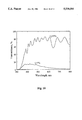
- a thin-film electrochromic coating was formed on a glass substrate by sequential vacuum deposition of the following layers: a transparent conductor of ITO, a counter electrode of Li y CrO 2+x ; a Li + ion conductor of Li 2 O-B 2 O 3 ; an electrochromic film of amorphous WO 3 ; and, a second transparent conductor of ITO. Details of the deposition processes are taught in Cogan and Rauh, U.S. Pat. No. 5,080,471. The minimum and maximum transmittance spectra of the coating are shown in FIG. 9 at an applied voltage of ⁇ 3 V. The coating has a luminous (photopic) transmittance range of 9% to 74% at these switching voltage levels.
- the electrochromic coating was then placed in a commercial PECVD system and a protective overlayer of a-SiOC:H deposited on the coating using the process conditions provided in Table 1.
- the thickness of the as-deposited a-SiOC:H was approximately 500 nm.
- the minimum and maximum transmittance spectra of the coating at ⁇ 3 V after a-SiOC:H deposition are shown in FIG. 10.
- the luminous transmittance range of the coating with the a-SiOC:H is 7% to 79%.
- a thin-film electrochromic coating was formed on a glass substrate in the manner described in Example 3.
- a protective overlayer comprising a 190 nm thick film of e-beam evaporated ZrO 2 , deposited at a substrate temperature of 100° C., and a 500 nm thick film of a-SiOC:H deposited in accordance with the conditions described in Table 1 was then deposited over the coating.
- FIG. 11 shows the spectral transmittance range of the coating.
- the photopic transmittance (T 1 ) varied from 11% to 77%.
Abstract
Description
α(hν)=A(hν-E.sub.o).sup.2
H.sub.2 O+e.sup.- =>OH.sup.- +1/2H.sub.2
              TABLE 1
______________________________________
Process Variable  Value
______________________________________
base pressure in chamber
                  <20 millitorr
process pressure  500 millitorr
process gases and flow rates:
Silane (2% in N.sub.2)
                  400 sccm
Methane           400 sccm
Nitrous oxide (100%)
                  16 sccm
substrate temperature
                  100° C.
RF power 13.56 MHz
                  120 watts (20 cm diameter
electrode-to-substrate distance
                  electrode)
                  approximately 2 cm
______________________________________
              TABLE 2
______________________________________
N.sub.2 O/
CH.sub.4  ratio
        thickness (nm)
                    E.sub.o (eV)
                            λ.sub.o (nm)
                                  T photopic (%)
______________________________________
0       316         2.12    585   60
1/8     510         3.00    414   89
1/4     537         3.02    411   90
5/12    1,470       3.27    380   88
2/3     472         3.78    328   88
______________________________________
Claims (8)
Priority Applications (1)
| Application Number | Priority Date | Filing Date | Title |
|---|---|---|---|
| US08/456,268 US5530581A (en) | 1995-05-31 | 1995-05-31 | Protective overlayer material and electro-optical coating using same |
Applications Claiming Priority (1)
| Application Number | Priority Date | Filing Date | Title |
|---|---|---|---|
| US08/456,268 US5530581A (en) | 1995-05-31 | 1995-05-31 | Protective overlayer material and electro-optical coating using same |
Publications (1)
| Publication Number | Publication Date |
|---|---|
| US5530581A true US5530581A (en) | 1996-06-25 |
Family
ID=23812121
Family Applications (1)
| Application Number | Title | Priority Date | Filing Date |
|---|---|---|---|
| US08/456,268 Expired - Fee Related US5530581A (en) | 1995-05-31 | 1995-05-31 | Protective overlayer material and electro-optical coating using same |
Country Status (1)
| Country | Link |
|---|---|
| US (1) | US5530581A (en) |
Cited By (86)
| Publication number | Priority date | Publication date | Assignee | Title |
|---|---|---|---|---|
| US5755759A (en) * | 1996-03-14 | 1998-05-26 | Eic Laboratories, Inc. | Biomedical device with a protective overlayer |
| US5886368A (en) * | 1997-07-29 | 1999-03-23 | Micron Technology, Inc. | Transistor with silicon oxycarbide gate and methods of fabrication and use |
| US5926740A (en) * | 1997-10-27 | 1999-07-20 | Micron Technology, Inc. | Graded anti-reflective coating for IC lithography |
| US6031263A (en) * | 1997-07-29 | 2000-02-29 | Micron Technology, Inc. | DEAPROM and transistor with gallium nitride or gallium aluminum nitride gate |
| US6091082A (en) * | 1998-02-17 | 2000-07-18 | Stmicroelectronics, Inc. | Electrostatic discharge protection for integrated circuit sensor passivation |
| US6114862A (en) * | 1996-02-14 | 2000-09-05 | Stmicroelectronics, Inc. | Capacitive distance sensor |
| US6159871A (en) * | 1998-05-29 | 2000-12-12 | Dow Corning Corporation | Method for producing hydrogenated silicon oxycarbide films having low dielectric constant |
| US6191593B1 (en) | 1997-12-17 | 2001-02-20 | Stmicroelectronics, Inc. | Method for the non-invasive sensing of physical matter on the detection surface of a capacitive sensor |
| US6287990B1 (en) | 1998-02-11 | 2001-09-11 | Applied Materials, Inc. | CVD plasma assisted low dielectric constant films |
| US6303523B2 (en) | 1998-02-11 | 2001-10-16 | Applied Materials, Inc. | Plasma processes for depositing low dielectric constant films |
| US6313518B1 (en) | 1997-10-14 | 2001-11-06 | Micron Technology, Inc. | Porous silicon oxycarbide integrated circuit insulator |
| US6320394B1 (en) | 1996-02-14 | 2001-11-20 | Stmicroelectronics S.R.L. | Capacitive distance sensor |
| US6362633B1 (en) | 1996-02-14 | 2002-03-26 | Stmicroelectronics S.R.L. | Capacitive distance sensor |
| US6372661B1 (en) * | 2000-07-14 | 2002-04-16 | Taiwan Semiconductor Manufacturing Company | Method to improve the crack resistance of CVD low-k dielectric constant material |
| US6492694B2 (en) | 1998-02-27 | 2002-12-10 | Micron Technology, Inc. | Highly conductive composite polysilicon gate for CMOS integrated circuits |
| US6504224B1 (en) | 1998-02-25 | 2003-01-07 | Micron Technology, Inc. | Methods and structures for metal interconnections in integrated circuits |
| FR2827396A1 (en) * | 2001-07-12 | 2003-01-17 | Saint Gobain | Lightweight electrochromic device, e.g. for anti-dazzle glazing or rear-view mirrors, has a functional film between two substrates with a low water vapor permeability, at least one of which is based on polymer film |
| US6512381B2 (en) | 1999-12-30 | 2003-01-28 | Stmicroelectronics, Inc. | Enhanced fingerprint detection |
| US6511903B1 (en) | 1998-02-11 | 2003-01-28 | Applied Materials, Inc. | Method of depositing a low k dielectric with organo silane |
| US6541859B1 (en) | 1998-02-25 | 2003-04-01 | Micron Technology, Inc. | Methods and structures for silver interconnections in integrated circuits |
| US6574404B2 (en) | 2000-01-31 | 2003-06-03 | Sumitomo Electric Industries, Ltd. | Choromatic dispersion compensating module and optical transmission system using the same |
| US6576980B1 (en) * | 1999-11-30 | 2003-06-10 | Agere Systems, Inc. | Surface treatment anneal of hydrogenated silicon-oxy-carbide dielectric layer |
| US6586797B2 (en) | 2001-08-30 | 2003-07-01 | Micron Technology, Inc. | Graded composition gate insulators to reduce tunneling barriers in flash memory devices |
| US6587097B1 (en) | 2000-11-28 | 2003-07-01 | 3M Innovative Properties Co. | Display system |
| US6610362B1 (en) * | 2000-11-20 | 2003-08-26 | Intel Corporation | Method of forming a carbon doped oxide layer on a substrate |
| US6660656B2 (en) | 1998-02-11 | 2003-12-09 | Applied Materials Inc. | Plasma processes for depositing low dielectric constant films |
| US6664589B2 (en) | 2001-08-30 | 2003-12-16 | Micron Technology, Inc. | Technique to control tunneling currents in DRAM capacitors, cells, and devices |
| US6667553B2 (en) * | 1998-05-29 | 2003-12-23 | Dow Corning Corporation | H:SiOC coated substrates |
| US20030235079A1 (en) * | 2002-06-21 | 2003-12-25 | Micron Technology, Inc. | Nor flash memory cell with high storage density |
| US20030235081A1 (en) * | 2002-06-21 | 2003-12-25 | Micron Technology, Inc. | Nanocrystal write once read only memory for archival storage |
| US20030234420A1 (en) * | 2002-06-21 | 2003-12-25 | Micron Technology, Inc. | Write once read only memory with large work function floating gates |
| US20030235085A1 (en) * | 2002-06-21 | 2003-12-25 | Micron Technology, Inc. | Write once read only memory employing charge trapping in insulators |
| US20030235066A1 (en) * | 2002-06-21 | 2003-12-25 | Micron Technology, Inc. | Ferroelectric write once read only memory for archival storage |
| US20040004859A1 (en) * | 2002-07-08 | 2004-01-08 | Micron Technology, Inc. | Memory utilizing oxide nanolaminates |
| US20040004247A1 (en) * | 2002-07-08 | 2004-01-08 | Micron Technology, Inc. | Memory utilizing oxide-nitride nanolaminates |
| US20040004245A1 (en) * | 2002-07-08 | 2004-01-08 | Micron Technology, Inc. | Memory utilizing oxide-conductor nanolaminates |
| US20040018362A1 (en) * | 2000-09-29 | 2004-01-29 | Tatsuji Nakajima | Silica layers and antireflection film using same |
| US6696157B1 (en) | 2000-03-05 | 2004-02-24 | 3M Innovative Properties Company | Diamond-like glass thin films |
| US6709721B2 (en) | 2001-03-28 | 2004-03-23 | Applied Materials Inc. | Purge heater design and process development for the improvement of low k film properties |
| US6731531B1 (en) | 1997-07-29 | 2004-05-04 | Micron Technology, Inc. | Carburized silicon gate insulators for integrated circuits |
| US6746893B1 (en) | 1997-07-29 | 2004-06-08 | Micron Technology, Inc. | Transistor with variable electron affinity gate and methods of fabrication and use |
| US20040119403A1 (en) * | 2002-12-19 | 2004-06-24 | 3M Innovative Properties Company | Organic electroluminescent device and encapsulation method |
| US20040164341A1 (en) * | 1997-07-29 | 2004-08-26 | Micron Technology, Inc. | Operating a memory device |
| US20040166240A1 (en) * | 2001-06-29 | 2004-08-26 | Shi-Woo Rhee | Method for preparing low dielectric films |
| US6795636B1 (en) | 2000-03-05 | 2004-09-21 | 3M Innovative Properties Company | Radiation-transmissive films on glass articles |
| US20040195967A1 (en) * | 2003-04-02 | 2004-10-07 | 3M Innovative Properties Company | Flexible high-temperature ultrabarrier |
| US20040226677A1 (en) * | 2000-05-26 | 2004-11-18 | Voith Paper Patent Gmbh | Process and a fluffer device for treatment of a fiber stock suspension |
| US6835638B1 (en) | 1997-07-29 | 2004-12-28 | Micron Technology, Inc. | Silicon carbide gate transistor and fabrication process |
| US6864139B2 (en) | 2000-02-29 | 2005-03-08 | Micron Technology, Inc. | Static NVRAM with ultra thin tunnel oxides |
| US6965123B1 (en) | 1997-07-29 | 2005-11-15 | Micron Technology, Inc. | Transistor with variable electron affinity gate and methods of fabrication and use |
| US20060001080A1 (en) * | 2002-06-21 | 2006-01-05 | Micron Technology, Inc. | Write once read only memory employing floating gates |
| US6987871B2 (en) | 1997-09-11 | 2006-01-17 | Upek, Inc. | Electrostatic discharge protection of a capacitive type fingerprint sensing array |
| US20060014027A1 (en) * | 2004-07-14 | 2006-01-19 | Afg Industries, Inc. | Silicon oxycarbide coatings having durable hydrophilic properties |
| US20060024878A1 (en) * | 1997-07-29 | 2006-02-02 | Micron Technology, Inc. | Deaprom having amorphous silicon carbide gate insulator |
| US20060025496A1 (en) * | 2004-08-02 | 2006-02-02 | Sunitha Grandhee | Decorative ink for automotive plastic glazing |
| US20060209223A1 (en) * | 2001-02-26 | 2006-09-21 | Samsung Electronic Co., Ltd. | Thin film transistor array substrate using low dielectric insulating layer and method of fabricating the same |
| US7142190B2 (en) * | 2002-02-28 | 2006-11-28 | Motorola, Inc. | Cellular communication handsets having variable appearance housings and methods therefor |
| US20060273375A1 (en) * | 1997-01-29 | 2006-12-07 | Micron Technology, Inc. | Transistor with nanocrystalline silicon gate structure |
| US20070020451A1 (en) * | 2005-07-20 | 2007-01-25 | 3M Innovative Properties Company | Moisture barrier coatings |
| US7239227B1 (en) | 1999-12-30 | 2007-07-03 | Upek, Inc. | Command interface using fingerprint sensor input system |
| US20080006819A1 (en) * | 2006-06-19 | 2008-01-10 | 3M Innovative Properties Company | Moisture barrier coatings for organic light emitting diode devices |
| US20080036384A1 (en) * | 2006-08-09 | 2008-02-14 | Chowdhury Ashfaqul I | Lamp with high reflectance end coat |
| US7429515B2 (en) | 2001-12-20 | 2008-09-30 | Micron Technology, Inc. | Low-temperature grown high quality ultra-thin CoTiO3 gate dielectrics |
| WO2009023482A1 (en) * | 2007-08-16 | 2009-02-19 | Dow Corning Corporation | Dichroic filters formed using silicon carbide based layers |
| US20090123039A1 (en) * | 2007-11-13 | 2009-05-14 | Upek, Inc. | Pixel Sensing Circuit with Common Mode Cancellation |
| US20090120496A1 (en) * | 2007-11-02 | 2009-05-14 | Agc Flat Glass North America, Inc. | Transparent conductive oxide coating for thin film photovoltaic applications and methods of making the same |
| US7642202B1 (en) * | 2001-06-28 | 2010-01-05 | Novellus Systems, Inc. | Methods of forming moisture barrier for low k film integration with anti-reflective layers |
| US20100068542A1 (en) * | 2006-12-29 | 2010-03-18 | 3M Innovative Properties Company | Method of making inorganic or inorganic/organic hybrid films |
| US20100068382A1 (en) * | 2006-12-29 | 2010-03-18 | Strobel Mark A | Method of curing metal alkoxide-containing films |
| US7709402B2 (en) | 2006-02-16 | 2010-05-04 | Micron Technology, Inc. | Conductive layers for hafnium silicon oxynitride films |
| WO2010119228A1 (en) * | 2009-04-16 | 2010-10-21 | Saint-Gobain Glass France | Electrochrome device with controlled transparency |
| US20100272933A1 (en) * | 2007-12-28 | 2010-10-28 | Mccormick Fred B | Flexible encapsulating film systems |
| US20100304090A1 (en) * | 2007-07-16 | 2010-12-02 | Christian Henn | Glass or glass-ceramic article coated with hard material and method for production thereof |
| US20110081502A1 (en) * | 2008-06-30 | 2011-04-07 | Bright Clark I | Method of making inorganic or inorganic/organic hybrid barrier films |
| US7927948B2 (en) | 2005-07-20 | 2011-04-19 | Micron Technology, Inc. | Devices with nanocrystals and methods of formation |
| US20110261429A1 (en) * | 2010-03-05 | 2011-10-27 | Sage Electrochromics, Inc. | Lamination of electrochromic device to glass substrates |
| US8114763B2 (en) | 2006-08-31 | 2012-02-14 | Micron Technology, Inc. | Tantalum aluminum oxynitride high-K dielectric |
| CN102597863A (en) * | 2009-08-31 | 2012-07-18 | 高丽大学校产学协力团 | Transparent structures |
| US8466016B2 (en) | 2006-08-31 | 2013-06-18 | Micron Technolgy, Inc. | Hafnium tantalum oxynitride dielectric |
| US8524618B2 (en) | 2005-01-05 | 2013-09-03 | Micron Technology, Inc. | Hafnium tantalum oxide dielectrics |
| US8685815B2 (en) | 2005-12-08 | 2014-04-01 | Micron Technology, Inc. | Hafnium tantalum titanium oxide films |
| US8765616B2 (en) | 2004-08-02 | 2014-07-01 | Micron Technology, Inc. | Zirconium-doped tantalum oxide films |
| US20150295200A1 (en) * | 2012-10-31 | 2015-10-15 | Konica Minolta, Inc. | Organic electroluminescent element |
| US9272941B2 (en) | 2012-04-05 | 2016-03-01 | Sage Electrochromics, Inc. | Method of cutting a panel using a starter crack and a glass panel including a starter crack |
| US10718937B2 (en) | 2010-07-16 | 2020-07-21 | Sage Electrochromics, Inc. | Electrochemical glazing having electrically controllable optical and energy-related properties |
| CN113422289A (en) * | 2021-05-21 | 2021-09-21 | 湖北光安伦芯片有限公司 | Communication laser semiconductor chip and manufacturing method thereof |
Citations (8)
| Publication number | Priority date | Publication date | Assignee | Title |
|---|---|---|---|---|
| US4350414A (en) * | 1979-06-26 | 1982-09-21 | Nippon Kogaku K. K. | All solid state electrochromic device |
| US4647472A (en) * | 1982-12-24 | 1987-03-03 | Tokyo Shibaura Denki Kabushiki Kaisha | Process of producing a semiconductor device |
| US4853251A (en) * | 1985-02-22 | 1989-08-01 | Canon Kabushiki Kaisha | Process for forming deposited film including carbon as a constituent element |
| US5080471A (en) * | 1990-04-06 | 1992-01-14 | Eic Laboratories, Inc. | Electrochromic material and electro-optical device using same |
| US5133594A (en) * | 1990-07-19 | 1992-07-28 | Tufts University | Transparent ion-blocking layer for electrochromic windows |
| US5136419A (en) * | 1990-03-06 | 1992-08-04 | The Dow Chemical Company | Sealed electrochromic device |
| US5216536A (en) * | 1991-11-26 | 1993-06-01 | Donnelly Corporation | Encapsulated electrochromic device and method for making same |
| US5238866A (en) * | 1991-09-11 | 1993-08-24 | GmbH & Co. Ingenieurburo Berlin Biotronik Mess- und Therapiegerate | Plasma enhanced chemical vapor deposition process for producing an amorphous semiconductive surface coating |
-
1995
- 1995-05-31 US US08/456,268 patent/US5530581A/en not_active Expired - Fee Related
Patent Citations (8)
| Publication number | Priority date | Publication date | Assignee | Title |
|---|---|---|---|---|
| US4350414A (en) * | 1979-06-26 | 1982-09-21 | Nippon Kogaku K. K. | All solid state electrochromic device |
| US4647472A (en) * | 1982-12-24 | 1987-03-03 | Tokyo Shibaura Denki Kabushiki Kaisha | Process of producing a semiconductor device |
| US4853251A (en) * | 1985-02-22 | 1989-08-01 | Canon Kabushiki Kaisha | Process for forming deposited film including carbon as a constituent element |
| US5136419A (en) * | 1990-03-06 | 1992-08-04 | The Dow Chemical Company | Sealed electrochromic device |
| US5080471A (en) * | 1990-04-06 | 1992-01-14 | Eic Laboratories, Inc. | Electrochromic material and electro-optical device using same |
| US5133594A (en) * | 1990-07-19 | 1992-07-28 | Tufts University | Transparent ion-blocking layer for electrochromic windows |
| US5238866A (en) * | 1991-09-11 | 1993-08-24 | GmbH & Co. Ingenieurburo Berlin Biotronik Mess- und Therapiegerate | Plasma enhanced chemical vapor deposition process for producing an amorphous semiconductive surface coating |
| US5216536A (en) * | 1991-11-26 | 1993-06-01 | Donnelly Corporation | Encapsulated electrochromic device and method for making same |
Non-Patent Citations (2)
| Title |
|---|
| Chang et al., "Novel Passivation Dielectrics--The boron--or Phosphorous--Doped Hydrogenated Amorphous Silicon Carbide Films," J. Electrochem. Soc., 132, 418-422 (1985). |
| Chang et al., Novel Passivation Dielectrics The boron or Phosphorous Doped Hydrogenated Amorphous Silicon Carbide Films, J. Electrochem. Soc., 132, 418 422 (1985). * |
Cited By (246)
| Publication number | Priority date | Publication date | Assignee | Title |
|---|---|---|---|---|
| US6320394B1 (en) | 1996-02-14 | 2001-11-20 | Stmicroelectronics S.R.L. | Capacitive distance sensor |
| US6496021B2 (en) * | 1996-02-14 | 2002-12-17 | Stmicroelectronics, Inc. | Method for making a capacitive distance sensor |
| US20040222803A1 (en) * | 1996-02-14 | 2004-11-11 | Marco Tartagni | Capacitive distance sensor |
| US6114862A (en) * | 1996-02-14 | 2000-09-05 | Stmicroelectronics, Inc. | Capacitive distance sensor |
| US6437583B1 (en) | 1996-02-14 | 2002-08-20 | Stmicroelectronics, Inc.. | Capacitive distance sensor |
| US6998855B2 (en) | 1996-02-14 | 2006-02-14 | Upek, Inc. | Capacitive distance sensor |
| US6362633B1 (en) | 1996-02-14 | 2002-03-26 | Stmicroelectronics S.R.L. | Capacitive distance sensor |
| US6731120B2 (en) | 1996-02-14 | 2004-05-04 | Stmicroelectronics, S.R.L. | Capacitive distance sensor |
| US5755759A (en) * | 1996-03-14 | 1998-05-26 | Eic Laboratories, Inc. | Biomedical device with a protective overlayer |
| US20060273375A1 (en) * | 1997-01-29 | 2006-12-07 | Micron Technology, Inc. | Transistor with nanocrystalline silicon gate structure |
| US7196929B1 (en) | 1997-07-29 | 2007-03-27 | Micron Technology Inc | Method for operating a memory device having an amorphous silicon carbide gate insulator |
| US6731531B1 (en) | 1997-07-29 | 2004-05-04 | Micron Technology, Inc. | Carburized silicon gate insulators for integrated circuits |
| US6307775B1 (en) | 1997-07-29 | 2001-10-23 | Micron Technology, Inc. | Deaprom and transistor with gallium nitride or gallium aluminum nitride gate |
| US6309907B1 (en) | 1997-07-29 | 2001-10-30 | Micron Technology, Inc. | Method of fabricating transistor with silicon oxycarbide gate |
| US6746893B1 (en) | 1997-07-29 | 2004-06-08 | Micron Technology, Inc. | Transistor with variable electron affinity gate and methods of fabrication and use |
| US6781876B2 (en) | 1997-07-29 | 2004-08-24 | Micron Technology, Inc. | Memory device with gallium nitride or gallium aluminum nitride gate |
| US7109548B2 (en) | 1997-07-29 | 2006-09-19 | Micron Technology, Inc. | Operating a memory device |
| US6249020B1 (en) | 1997-07-29 | 2001-06-19 | Micron Technology, Inc. | DEAPROM and transistor with gallium nitride or gallium aluminum nitride gate |
| US20040164341A1 (en) * | 1997-07-29 | 2004-08-26 | Micron Technology, Inc. | Operating a memory device |
| US6835638B1 (en) | 1997-07-29 | 2004-12-28 | Micron Technology, Inc. | Silicon carbide gate transistor and fabrication process |
| US6794255B1 (en) | 1997-07-29 | 2004-09-21 | Micron Technology, Inc. | Carburized silicon gate insulators for integrated circuits |
| US6762068B1 (en) | 1997-07-29 | 2004-07-13 | Micron Technology, Inc. | Transistor with variable electron affinity gate and methods of fabrication and use |
| US7005344B2 (en) | 1997-07-29 | 2006-02-28 | Micron Technology, Inc. | Method of forming a device with a gallium nitride or gallium aluminum nitride gate |
| US6031263A (en) * | 1997-07-29 | 2000-02-29 | Micron Technology, Inc. | DEAPROM and transistor with gallium nitride or gallium aluminum nitride gate |
| US6936849B1 (en) | 1997-07-29 | 2005-08-30 | Micron Technology, Inc. | Silicon carbide gate transistor |
| US20060024878A1 (en) * | 1997-07-29 | 2006-02-02 | Micron Technology, Inc. | Deaprom having amorphous silicon carbide gate insulator |
| US20060017095A1 (en) * | 1997-07-29 | 2006-01-26 | Micron Technology, Inc. | Carburized silicon gate insulators for integrated circuits |
| US7169666B2 (en) | 1997-07-29 | 2007-01-30 | Micron Technology, Inc. | Method of forming a device having a gate with a selected electron affinity |
| US7154153B1 (en) | 1997-07-29 | 2006-12-26 | Micron Technology, Inc. | Memory device |
| US7242049B2 (en) | 1997-07-29 | 2007-07-10 | Micron Technology, Inc. | Memory device |
| US6965123B1 (en) | 1997-07-29 | 2005-11-15 | Micron Technology, Inc. | Transistor with variable electron affinity gate and methods of fabrication and use |
| US7141824B2 (en) | 1997-07-29 | 2006-11-28 | Micron Technology, Inc. | Transistor with variable electron affinity gate |
| US5886368A (en) * | 1997-07-29 | 1999-03-23 | Micron Technology, Inc. | Transistor with silicon oxycarbide gate and methods of fabrication and use |
| US6987871B2 (en) | 1997-09-11 | 2006-01-17 | Upek, Inc. | Electrostatic discharge protection of a capacitive type fingerprint sensing array |
| US6710428B2 (en) | 1997-10-14 | 2004-03-23 | Micron Technology, Inc. | Porous silicon oxycarbide integrated circuit insulator |
| US6350704B1 (en) | 1997-10-14 | 2002-02-26 | Micron Technology Inc. | Porous silicon oxycarbide integrated circuit insulator |
| US6803326B2 (en) | 1997-10-14 | 2004-10-12 | Micron Technology, Inc. | Porous silicon oxycarbide integrated circuit insulator |
| US6313518B1 (en) | 1997-10-14 | 2001-11-06 | Micron Technology, Inc. | Porous silicon oxycarbide integrated circuit insulator |
| US5926740A (en) * | 1997-10-27 | 1999-07-20 | Micron Technology, Inc. | Graded anti-reflective coating for IC lithography |
| US6191593B1 (en) | 1997-12-17 | 2001-02-20 | Stmicroelectronics, Inc. | Method for the non-invasive sensing of physical matter on the detection surface of a capacitive sensor |
| US7560377B2 (en) | 1998-02-11 | 2009-07-14 | Applied Materials, Inc. | Plasma processes for depositing low dielectric constant films |
| US20040147109A1 (en) * | 1998-02-11 | 2004-07-29 | Applied Materials, Inc. | Low dielectric constant film produced from silicon compounds comprising silicon-carbon bond |
| US20080061439A1 (en) * | 1998-02-11 | 2008-03-13 | Wai-Fan Yau | Low dielectric constant film produced from silicon compounds comprising silicon-carbon bond |
| US6660663B1 (en) | 1998-02-11 | 2003-12-09 | Applied Materials Inc. | Computer readable medium for holding a program for performing plasma-assisted CVD of low dielectric constant films formed from organosilane compounds |
| US6660656B2 (en) | 1998-02-11 | 2003-12-09 | Applied Materials Inc. | Plasma processes for depositing low dielectric constant films |
| US6562690B1 (en) | 1998-02-11 | 2003-05-13 | Applied Materials, Inc. | Plasma processes for depositing low dielectric constant films |
| US6287990B1 (en) | 1998-02-11 | 2001-09-11 | Applied Materials, Inc. | CVD plasma assisted low dielectric constant films |
| US6541282B1 (en) | 1998-02-11 | 2003-04-01 | Applied Materials, Inc. | Plasma processes for depositing low dielectric constant films |
| US6537929B1 (en) | 1998-02-11 | 2003-03-25 | Applied Materials, Inc. | CVD plasma assisted low dielectric constant films |
| US6511903B1 (en) | 1998-02-11 | 2003-01-28 | Applied Materials, Inc. | Method of depositing a low k dielectric with organo silane |
| US7651725B2 (en) | 1998-02-11 | 2010-01-26 | Applied Materials, Inc. | Low dielectric constant film produced from silicon compounds comprising silicon-carbon bond |
| US6730593B2 (en) | 1998-02-11 | 2004-05-04 | Applied Materials Inc. | Method of depositing a low K dielectric with organo silane |
| US20050191846A1 (en) * | 1998-02-11 | 2005-09-01 | David Cheung | Plasma processes for depositing low dielectric constant films |
| US6348725B2 (en) | 1998-02-11 | 2002-02-19 | Applied Materials, Inc. | Plasma processes for depositing low dielectric constant films |
| US6303523B2 (en) | 1998-02-11 | 2001-10-16 | Applied Materials, Inc. | Plasma processes for depositing low dielectric constant films |
| US20080064225A1 (en) * | 1998-02-11 | 2008-03-13 | Wai-Fan Yau | Low dielectric constant film produced from silicon compounds comprising silicon-carbon bond |
| US6596655B1 (en) | 1998-02-11 | 2003-07-22 | Applied Materials Inc. | Plasma processes for depositing low dielectric constant films |
| US20050156317A1 (en) * | 1998-02-11 | 2005-07-21 | Applied Materials, Inc. | Low dielectric constant film produced from silicon compounds comprising silicon-carbon bonds |
| US6180989B1 (en) | 1998-02-17 | 2001-01-30 | Stmicroelectronics, Inc. | Selectively doped electrostatic discharge layer for an integrated circuit sensor |
| US6472246B1 (en) | 1998-02-17 | 2002-10-29 | Stmicroelectronics, Inc. | Electrostatic discharge protection for integrated circuit sensor passivation |
| US6610555B1 (en) | 1998-02-17 | 2003-08-26 | Stmicroelectronics, Inc. | Selectively doped electrostatic discharge layer for an integrated circuit sensor |
| US6091082A (en) * | 1998-02-17 | 2000-07-18 | Stmicroelectronics, Inc. | Electrostatic discharge protection for integrated circuit sensor passivation |
| US20050186773A1 (en) * | 1998-02-25 | 2005-08-25 | Micron Technology, Inc. | Methods and structures for metal interconnections in integrated circuits |
| US6879017B2 (en) | 1998-02-25 | 2005-04-12 | Micron Technology, Inc. | Methods and structures for metal interconnections in integrated circuits |
| US7186664B2 (en) | 1998-02-25 | 2007-03-06 | Micron Technology, Inc. | Methods and structures for metal interconnections in integrated circuits |
| US6504224B1 (en) | 1998-02-25 | 2003-01-07 | Micron Technology, Inc. | Methods and structures for metal interconnections in integrated circuits |
| US6541859B1 (en) | 1998-02-25 | 2003-04-01 | Micron Technology, Inc. | Methods and structures for silver interconnections in integrated circuits |
| US20030209775A1 (en) * | 1998-02-25 | 2003-11-13 | Micron Technology, Inc. | Methods and structures for metal interconnections in integrated circuits |
| US6492694B2 (en) | 1998-02-27 | 2002-12-10 | Micron Technology, Inc. | Highly conductive composite polysilicon gate for CMOS integrated circuits |
| US6573169B2 (en) | 1998-02-27 | 2003-06-03 | Micron Technology, Inc. | Highly conductive composite polysilicon gate for CMOS integrated circuits |
| US6593655B1 (en) * | 1998-05-29 | 2003-07-15 | Dow Corning Corporation | Method for producing hydrogenated silicon oxycarbide films having low dielectric constant |
| US6159871A (en) * | 1998-05-29 | 2000-12-12 | Dow Corning Corporation | Method for producing hydrogenated silicon oxycarbide films having low dielectric constant |
| US6667553B2 (en) * | 1998-05-29 | 2003-12-23 | Dow Corning Corporation | H:SiOC coated substrates |
| US6576980B1 (en) * | 1999-11-30 | 2003-06-10 | Agere Systems, Inc. | Surface treatment anneal of hydrogenated silicon-oxy-carbide dielectric layer |
| US7239227B1 (en) | 1999-12-30 | 2007-07-03 | Upek, Inc. | Command interface using fingerprint sensor input system |
| US6512381B2 (en) | 1999-12-30 | 2003-01-28 | Stmicroelectronics, Inc. | Enhanced fingerprint detection |
| US6574404B2 (en) | 2000-01-31 | 2003-06-03 | Sumitomo Electric Industries, Ltd. | Choromatic dispersion compensating module and optical transmission system using the same |
| US6864139B2 (en) | 2000-02-29 | 2005-03-08 | Micron Technology, Inc. | Static NVRAM with ultra thin tunnel oxides |
| US6696157B1 (en) | 2000-03-05 | 2004-02-24 | 3M Innovative Properties Company | Diamond-like glass thin films |
| US6795636B1 (en) | 2000-03-05 | 2004-09-21 | 3M Innovative Properties Company | Radiation-transmissive films on glass articles |
| US7496255B2 (en) | 2000-03-05 | 2009-02-24 | 3M Innovative Properties Company | Radiation-transmissive films on glass articles |
| US20040226677A1 (en) * | 2000-05-26 | 2004-11-18 | Voith Paper Patent Gmbh | Process and a fluffer device for treatment of a fiber stock suspension |
| US6372661B1 (en) * | 2000-07-14 | 2002-04-16 | Taiwan Semiconductor Manufacturing Company | Method to improve the crack resistance of CVD low-k dielectric constant material |
| US20040018362A1 (en) * | 2000-09-29 | 2004-01-29 | Tatsuji Nakajima | Silica layers and antireflection film using same |
| US6838197B2 (en) * | 2000-09-29 | 2005-01-04 | Dai Nippon Printing Co., Ltd. | Silica layers and antireflection film using same |
| US6610362B1 (en) * | 2000-11-20 | 2003-08-26 | Intel Corporation | Method of forming a carbon doped oxide layer on a substrate |
| US6762435B2 (en) | 2000-11-20 | 2004-07-13 | Intel Corporation | Semiconductor device with boron containing carbon doped silicon oxide layer |
| US6587097B1 (en) | 2000-11-28 | 2003-07-01 | 3M Innovative Properties Co. | Display system |
| US20060209223A1 (en) * | 2001-02-26 | 2006-09-21 | Samsung Electronic Co., Ltd. | Thin film transistor array substrate using low dielectric insulating layer and method of fabricating the same |
| US7615783B2 (en) * | 2001-02-26 | 2009-11-10 | Samsung Electronics Co., Ltd. | Thin film transistor array substrate using low dielectric insulating layer and method of fabricating the same |
| US6709721B2 (en) | 2001-03-28 | 2004-03-23 | Applied Materials Inc. | Purge heater design and process development for the improvement of low k film properties |
| US8003549B1 (en) | 2001-06-28 | 2011-08-23 | Novellus Systems, Inc. | Methods of forming moisture barrier for low K film integration with anti-reflective layers |
| US7642202B1 (en) * | 2001-06-28 | 2010-01-05 | Novellus Systems, Inc. | Methods of forming moisture barrier for low k film integration with anti-reflective layers |
| US20040166240A1 (en) * | 2001-06-29 | 2004-08-26 | Shi-Woo Rhee | Method for preparing low dielectric films |
| US7087271B2 (en) * | 2001-06-29 | 2006-08-08 | Postech Foundation | Method for preparing low dielectric films |
| WO2003007065A1 (en) * | 2001-07-12 | 2003-01-23 | Saint-Gobain Glass France | Electrically controllable controllable device having variable optical and/or energetic properties |
| US7002720B2 (en) | 2001-07-12 | 2006-02-21 | Saint-Gobain Glass France | Electrically controllable device having variable optical and/or energy properties |
| US20040233499A1 (en) * | 2001-07-12 | 2004-11-25 | Fabien Betelle | Electrically controllable controllable device having variable optical and/or energetic properties |
| CN1308760C (en) * | 2001-07-12 | 2007-04-04 | 法国圣戈班玻璃厂 | Electrically controllable device having variable optical and/or energetic properties |
| FR2827396A1 (en) * | 2001-07-12 | 2003-01-17 | Saint Gobain | Lightweight electrochromic device, e.g. for anti-dazzle glazing or rear-view mirrors, has a functional film between two substrates with a low water vapor permeability, at least one of which is based on polymer film |
| US6955968B2 (en) | 2001-08-30 | 2005-10-18 | Micron Technology Inc. | Graded composition gate insulators to reduce tunneling barriers in flash memory devices |
| US6979607B2 (en) | 2001-08-30 | 2005-12-27 | Micron Technology, Inc. | Technique to control tunneling currents in DRAM capacitors, cells, and devices |
| US20070228438A1 (en) * | 2001-08-30 | 2007-10-04 | Micron Technology, Inc. | Technique to control tunneling currents in dram capacitors, cells, and devices |
| US20040106251A1 (en) * | 2001-08-30 | 2004-06-03 | Micron Technology, Inc. | Technique to control tunneling currents in DRAM capacitors, cells, and devices |
| US6586797B2 (en) | 2001-08-30 | 2003-07-01 | Micron Technology, Inc. | Graded composition gate insulators to reduce tunneling barriers in flash memory devices |
| US6664589B2 (en) | 2001-08-30 | 2003-12-16 | Micron Technology, Inc. | Technique to control tunneling currents in DRAM capacitors, cells, and devices |
| US7235837B2 (en) | 2001-08-30 | 2007-06-26 | Micron Technology, Inc. | Technique to control tunneling currents in DRAM capacitors, cells, and devices |
| US20060054956A1 (en) * | 2001-08-30 | 2006-03-16 | Micron Technology, Inc. | Technique to control tunneling currents in DRAM capacitors, cells, and devices |
| US20040104426A1 (en) * | 2001-08-30 | 2004-06-03 | Micron Technology, Inc. | Graded composition gate insulators to reduce tunneling barriers in flash memory devices |
| US7429515B2 (en) | 2001-12-20 | 2008-09-30 | Micron Technology, Inc. | Low-temperature grown high quality ultra-thin CoTiO3 gate dielectrics |
| US8178413B2 (en) | 2001-12-20 | 2012-05-15 | Micron Technology, Inc. | Low-temperature grown high quality ultra-thin CoTiO3 gate dielectrics |
| US7804144B2 (en) | 2001-12-20 | 2010-09-28 | Micron Technology, Inc. | Low-temperature grown high quality ultra-thin CoTiO3 gate dielectrics |
| US7142190B2 (en) * | 2002-02-28 | 2006-11-28 | Motorola, Inc. | Cellular communication handsets having variable appearance housings and methods therefor |
| US7130220B2 (en) | 2002-06-21 | 2006-10-31 | Micron Technology, Inc. | Write once read only memory employing floating gates |
| US20030235085A1 (en) * | 2002-06-21 | 2003-12-25 | Micron Technology, Inc. | Write once read only memory employing charge trapping in insulators |
| US20030235079A1 (en) * | 2002-06-21 | 2003-12-25 | Micron Technology, Inc. | Nor flash memory cell with high storage density |
| US20030234420A1 (en) * | 2002-06-21 | 2003-12-25 | Micron Technology, Inc. | Write once read only memory with large work function floating gates |
| US20030235081A1 (en) * | 2002-06-21 | 2003-12-25 | Micron Technology, Inc. | Nanocrystal write once read only memory for archival storage |
| US20030235066A1 (en) * | 2002-06-21 | 2003-12-25 | Micron Technology, Inc. | Ferroelectric write once read only memory for archival storage |
| US7639528B2 (en) | 2002-06-21 | 2009-12-29 | Micron Technology, Inc. | Nanocrystal write once read only memory for archival storage |
| US7113429B2 (en) | 2002-06-21 | 2006-09-26 | Micron Technology, Inc. | Nor flash memory cell with high storage density |
| US7112494B2 (en) | 2002-06-21 | 2006-09-26 | Micron Technology, Inc. | Write once read only memory employing charge trapping in insulators |
| US20060001080A1 (en) * | 2002-06-21 | 2006-01-05 | Micron Technology, Inc. | Write once read only memory employing floating gates |
| US7133315B2 (en) | 2002-06-21 | 2006-11-07 | Micron Technology, Inc. | Write once read only memory employing charge trapping in insulators |
| US7476586B2 (en) | 2002-06-21 | 2009-01-13 | Micron Technology, Inc. | NOR flash memory cell with high storage density |
| US7369435B2 (en) | 2002-06-21 | 2008-05-06 | Micron Technology, Inc. | Write once read only memory employing floating gates |
| US7348237B2 (en) | 2002-06-21 | 2008-03-25 | Micron Technology, Inc. | NOR flash memory cell with high storage density |
| US6970370B2 (en) | 2002-06-21 | 2005-11-29 | Micron Technology, Inc. | Ferroelectric write once read only memory for archival storage |
| US20040130951A1 (en) * | 2002-06-21 | 2004-07-08 | Micron Technology, Inc. | Write once read only memory employing charge trapping in insulators |
| US7154140B2 (en) | 2002-06-21 | 2006-12-26 | Micron Technology, Inc. | Write once read only memory with large work function floating gates |
| US7154778B2 (en) | 2002-06-21 | 2006-12-26 | Micron Technology, Inc. | Nanocrystal write once read only memory for archival storage |
| US6952362B2 (en) | 2002-06-21 | 2005-10-04 | Micron Technology, Inc. | Ferroelectric write once read only memory for archival storage |
| US20040165412A1 (en) * | 2002-06-21 | 2004-08-26 | Micron Technology, Inc. | Ferroelectric write once read only memory for archival storage |
| US7166509B2 (en) | 2002-06-21 | 2007-01-23 | Micron Technology, Inc. | Write once read only memory with large work function floating gates |
| US20080062757A1 (en) * | 2002-06-21 | 2008-03-13 | Micron Technology, Inc. | Nanocrystal write once read only memory for archival storage |
| US20050199947A1 (en) * | 2002-06-21 | 2005-09-15 | Micron Technology, Inc. | Nanocrystal write once read only memory for archival storage |
| US6888739B2 (en) | 2002-06-21 | 2005-05-03 | Micron Technology Inc. | Nanocrystal write once read only memory for archival storage |
| US7193893B2 (en) | 2002-06-21 | 2007-03-20 | Micron Technology, Inc. | Write once read only memory employing floating gates |
| US20050082599A1 (en) * | 2002-06-21 | 2005-04-21 | Micron Technology, Inc. | Nor flash memory cell with high storage density |
| US20050036370A1 (en) * | 2002-06-21 | 2005-02-17 | Micron Technology, Inc. | Write once read only memory with large work function floating gates |
| US6996009B2 (en) | 2002-06-21 | 2006-02-07 | Micron Technology, Inc. | NOR flash memory cell with high storage density |
| US7257022B2 (en) | 2002-06-21 | 2007-08-14 | Micron Technology, Inc. | Nanocrystal write once read only memory for archival storage |
| US6804136B2 (en) | 2002-06-21 | 2004-10-12 | Micron Technology, Inc. | Write once read only memory employing charge trapping in insulators |
| US20050026375A1 (en) * | 2002-06-21 | 2005-02-03 | Micron Technology, Inc. | Write once read only memory employing charge trapping in insulators |
| US7489545B2 (en) | 2002-07-08 | 2009-02-10 | Micron Technology, Inc. | Memory utilizing oxide-nitride nanolaminates |
| US20060008966A1 (en) * | 2002-07-08 | 2006-01-12 | Micron Technology, Inc. | Memory utilizing oxide-conductor nanolaminates |
| US7583534B2 (en) | 2002-07-08 | 2009-09-01 | Micron Technolgy, Inc. | Memory utilizing oxide-conductor nanolaminates |
| US20060258097A1 (en) * | 2002-07-08 | 2006-11-16 | Micron Technology, Inc. | Memory utilizing oxide-nitride nanolaminates |
| US7433237B2 (en) | 2002-07-08 | 2008-10-07 | Micron Technology, Inc. | Memory utilizing oxide nanolaminates |
| US7728626B2 (en) | 2002-07-08 | 2010-06-01 | Micron Technology, Inc. | Memory utilizing oxide nanolaminates |
| US20040004859A1 (en) * | 2002-07-08 | 2004-01-08 | Micron Technology, Inc. | Memory utilizing oxide nanolaminates |
| US20040004245A1 (en) * | 2002-07-08 | 2004-01-08 | Micron Technology, Inc. | Memory utilizing oxide-conductor nanolaminates |
| US7494873B2 (en) | 2002-07-08 | 2009-02-24 | Micron Technology, Inc. | Memory utilizing oxide-nitride nanolaminates |
| US20060261376A1 (en) * | 2002-07-08 | 2006-11-23 | Micron Technology, Inc. | Memory utilizing oxide-nitride nanolaminates |
| US7847344B2 (en) | 2002-07-08 | 2010-12-07 | Micron Technology, Inc. | Memory utilizing oxide-nitride nanolaminates |
| US8228725B2 (en) | 2002-07-08 | 2012-07-24 | Micron Technology, Inc. | Memory utilizing oxide nanolaminates |
| US7221017B2 (en) | 2002-07-08 | 2007-05-22 | Micron Technology, Inc. | Memory utilizing oxide-conductor nanolaminates |
| US7687848B2 (en) | 2002-07-08 | 2010-03-30 | Micron Technology, Inc. | Memory utilizing oxide-conductor nanolaminates |
| US20050023574A1 (en) * | 2002-07-08 | 2005-02-03 | Micron Technology, Inc. | Memory utilizing oxide-nitride nanolaminates |
| US20040004247A1 (en) * | 2002-07-08 | 2004-01-08 | Micron Technology, Inc. | Memory utilizing oxide-nitride nanolaminates |
| US7221586B2 (en) | 2002-07-08 | 2007-05-22 | Micron Technology, Inc. | Memory utilizing oxide nanolaminates |
| US6975067B2 (en) | 2002-12-19 | 2005-12-13 | 3M Innovative Properties Company | Organic electroluminescent device and encapsulation method |
| US20050247400A1 (en) * | 2002-12-19 | 2005-11-10 | 3M Innovative Properties Company | Organic electroluminescent device and encapsulation method |
| US7156942B2 (en) | 2002-12-19 | 2007-01-02 | 3M Innovative Properties Company | Organic electroluminescent device and encapsulation method |
| US20040119403A1 (en) * | 2002-12-19 | 2004-06-24 | 3M Innovative Properties Company | Organic electroluminescent device and encapsulation method |
| US7486019B2 (en) | 2003-04-02 | 2009-02-03 | 3M Innovative Properties Company | Flexible high-temperature ultrabarrier |
| US20060062937A1 (en) * | 2003-04-02 | 2006-03-23 | 3M Innovative Properties Company | Flexible high-temperature ultrabarrier |
| US20090142476A1 (en) * | 2003-04-02 | 2009-06-04 | 3M Innovative Properties Company | Flexible high-temperature ultrabarrier |
| US7980910B2 (en) | 2003-04-02 | 2011-07-19 | 3M Innovative Properties Company | Flexible high-temperature ultrabarrier |
| US7940004B2 (en) | 2003-04-02 | 2011-05-10 | 3M Innovative Properties Company | Flexible high-temperature ultrabarrier |
| EP2277698A1 (en) | 2003-04-02 | 2011-01-26 | 3M Innovative Properties Company | Flexible high-temperature ultrabarrier |
| US20040195967A1 (en) * | 2003-04-02 | 2004-10-07 | 3M Innovative Properties Company | Flexible high-temperature ultrabarrier |
| EP3121003A1 (en) | 2003-04-02 | 2017-01-25 | 3M Innovative Properties Company | Flexible high-temperature ultrabarrier |
| US7018713B2 (en) | 2003-04-02 | 2006-03-28 | 3M Innovative Properties Company | Flexible high-temperature ultrabarrier |
| US20100119840A1 (en) * | 2003-04-02 | 2010-05-13 | 3M Innovative Properties Company | Flexible high-temperature ultrabarrier |
| US20100073936A1 (en) * | 2003-04-02 | 2010-03-25 | 3M Innovative Properties Comapny | Flexible high-temperature ultrabarrier |
| US7482060B2 (en) | 2004-07-14 | 2009-01-27 | Agc Flat Glass North America, Inc. | Silicon oxycarbide coatings having durable hydrophilic properties |
| US20060014027A1 (en) * | 2004-07-14 | 2006-01-19 | Afg Industries, Inc. | Silicon oxycarbide coatings having durable hydrophilic properties |
| US7732041B2 (en) * | 2004-08-02 | 2010-06-08 | Exatec Llc | Decorative ink for automotive plastic glazing |
| US8765616B2 (en) | 2004-08-02 | 2014-07-01 | Micron Technology, Inc. | Zirconium-doped tantalum oxide films |
| US20060025496A1 (en) * | 2004-08-02 | 2006-02-02 | Sunitha Grandhee | Decorative ink for automotive plastic glazing |
| US8524618B2 (en) | 2005-01-05 | 2013-09-03 | Micron Technology, Inc. | Hafnium tantalum oxide dielectrics |
| EP2857443A1 (en) | 2005-07-20 | 2015-04-08 | 3M Innovative Properties Company | Moisture barrier coatings |
| US7927948B2 (en) | 2005-07-20 | 2011-04-19 | Micron Technology, Inc. | Devices with nanocrystals and methods of formation |
| US8501563B2 (en) | 2005-07-20 | 2013-08-06 | Micron Technology, Inc. | Devices with nanocrystals and methods of formation |
| US8288818B2 (en) | 2005-07-20 | 2012-10-16 | Micron Technology, Inc. | Devices with nanocrystals and methods of formation |
| US20090186209A1 (en) * | 2005-07-20 | 2009-07-23 | 3M Innovative Properties Company | Moisture barrier coatings |
| US20090169770A1 (en) * | 2005-07-20 | 2009-07-02 | 3M Innovative Properties Company | Moisture barrier coatings |
| US8921914B2 (en) | 2005-07-20 | 2014-12-30 | Micron Technology, Inc. | Devices with nanocrystals and methods of formation |
| US20070020451A1 (en) * | 2005-07-20 | 2007-01-25 | 3M Innovative Properties Company | Moisture barrier coatings |
| US20110143129A1 (en) * | 2005-07-20 | 2011-06-16 | 3M Innovative Properties Company | Moisture barrier coatings |
| US8034452B2 (en) | 2005-07-20 | 2011-10-11 | 3M Innovative Properties Company | Moisture barrier coatings |
| US8685815B2 (en) | 2005-12-08 | 2014-04-01 | Micron Technology, Inc. | Hafnium tantalum titanium oxide films |
| US8785312B2 (en) | 2006-02-16 | 2014-07-22 | Micron Technology, Inc. | Conductive layers for hafnium silicon oxynitride |
| US8067794B2 (en) | 2006-02-16 | 2011-11-29 | Micron Technology, Inc. | Conductive layers for hafnium silicon oxynitride films |
| US7709402B2 (en) | 2006-02-16 | 2010-05-04 | Micron Technology, Inc. | Conductive layers for hafnium silicon oxynitride films |
| US20080006819A1 (en) * | 2006-06-19 | 2008-01-10 | 3M Innovative Properties Company | Moisture barrier coatings for organic light emitting diode devices |
| US20090252894A1 (en) * | 2006-06-19 | 2009-10-08 | 3M Innovative Properties Company | Moisture barrier coatings for organic light emitting diode devices |
| US20080036384A1 (en) * | 2006-08-09 | 2008-02-14 | Chowdhury Ashfaqul I | Lamp with high reflectance end coat |
| US8759170B2 (en) | 2006-08-31 | 2014-06-24 | Micron Technology, Inc. | Hafnium tantalum oxynitride dielectric |
| US8114763B2 (en) | 2006-08-31 | 2012-02-14 | Micron Technology, Inc. | Tantalum aluminum oxynitride high-K dielectric |
| US8466016B2 (en) | 2006-08-31 | 2013-06-18 | Micron Technolgy, Inc. | Hafnium tantalum oxynitride dielectric |
| US20100068542A1 (en) * | 2006-12-29 | 2010-03-18 | 3M Innovative Properties Company | Method of making inorganic or inorganic/organic hybrid films |
| US20100068382A1 (en) * | 2006-12-29 | 2010-03-18 | Strobel Mark A | Method of curing metal alkoxide-containing films |
| US8227040B2 (en) | 2006-12-29 | 2012-07-24 | 3M Innovative Properties Company | Method of curing metal alkoxide-containing films |
| US20100304090A1 (en) * | 2007-07-16 | 2010-12-02 | Christian Henn | Glass or glass-ceramic article coated with hard material and method for production thereof |
| US8460804B2 (en) * | 2007-07-16 | 2013-06-11 | Schott Ag | Glass or glass-ceramic article coated with hard material and method for production thereof |
| EP2538248A1 (en) * | 2007-08-16 | 2012-12-26 | Dow Corning Corporation | Dichroic filters formed using silicon carbide based layers |
| WO2009023482A1 (en) * | 2007-08-16 | 2009-02-19 | Dow Corning Corporation | Dichroic filters formed using silicon carbide based layers |
| CN101980986B (en) * | 2007-11-02 | 2016-04-27 | 北美Agc平板玻璃公司 | For transparent conductive oxide coating and the production method thereof of film photovoltaic application |
| US20090120496A1 (en) * | 2007-11-02 | 2009-05-14 | Agc Flat Glass North America, Inc. | Transparent conductive oxide coating for thin film photovoltaic applications and methods of making the same |
| CN101980986A (en) * | 2007-11-02 | 2011-02-23 | 北美Agc平板玻璃公司 | Transparent conductive oxide coating for thin film photovoltaic applications and methods of making the same |
| US9181124B2 (en) * | 2007-11-02 | 2015-11-10 | Agc Flat Glass North America, Inc. | Transparent conductive oxide coating for thin film photovoltaic applications and methods of making the same |
| US8115497B2 (en) | 2007-11-13 | 2012-02-14 | Authentec, Inc. | Pixel sensing circuit with common mode cancellation |
| US20090123039A1 (en) * | 2007-11-13 | 2009-05-14 | Upek, Inc. | Pixel Sensing Circuit with Common Mode Cancellation |
| US20100272933A1 (en) * | 2007-12-28 | 2010-10-28 | Mccormick Fred B | Flexible encapsulating film systems |
| US8846169B2 (en) | 2007-12-28 | 2014-09-30 | 3M Innovative Properties Company | Flexible encapsulating film systems |
| US9481927B2 (en) | 2008-06-30 | 2016-11-01 | 3M Innovative Properties Company | Method of making inorganic or inorganic/organic hybrid barrier films |
| US20110081502A1 (en) * | 2008-06-30 | 2011-04-07 | Bright Clark I | Method of making inorganic or inorganic/organic hybrid barrier films |
| WO2010119228A1 (en) * | 2009-04-16 | 2010-10-21 | Saint-Gobain Glass France | Electrochrome device with controlled transparency |
| CN102460292A (en) * | 2009-04-16 | 2012-05-16 | 法国圣戈班玻璃厂 | Electrochrome device with controlled transparency |
| US20120019889A1 (en) * | 2009-04-16 | 2012-01-26 | Saint- Gobain Glass France | Controlled-transparency electrochromic device |
| US8405896B2 (en) * | 2009-04-16 | 2013-03-26 | Saint-Gobain Glass France | Controlled-transparency electrochromic device |
| FR2944610A1 (en) * | 2009-04-16 | 2010-10-22 | Saint Gobain | ELECTROCHROME DEVICE HAVING CONTROLLED TRANSPARENCY |
| CN102460292B (en) * | 2009-04-16 | 2014-07-30 | 塞奇电致变色公司 | Electrochrome device with controlled transparency |
| JP2012524290A (en) * | 2009-04-16 | 2012-10-11 | セイジ・エレクトロクロミクス,インコーポレイテッド | Transparency controlled electrochromic device |
| CN102597863A (en) * | 2009-08-31 | 2012-07-18 | 高丽大学校产学协力团 | Transparent structures |
| CN102883880B (en) * | 2010-03-05 | 2017-02-08 | Sage电致变色显示有限公司 | Lamination of electrochromic device to glass substrates |
| US20110261429A1 (en) * | 2010-03-05 | 2011-10-27 | Sage Electrochromics, Inc. | Lamination of electrochromic device to glass substrates |
| US20110267672A1 (en) * | 2010-03-05 | 2011-11-03 | Sage Electrochromics, Inc. | Lamination of electrochromic device to glass substrates |
| US9182644B2 (en) | 2010-03-05 | 2015-11-10 | Sage Electrochromics, Inc. | Lamination of electrochromic device to glass substrates |
| US11890835B2 (en) | 2010-03-05 | 2024-02-06 | Sage Electrochromics, Inc. | Lamination of electrochromic device to glass substrates |
| US9316883B2 (en) | 2010-03-05 | 2016-04-19 | Sage Electrochromics, Inc. | Lamination of electrochromic device to glass substrates |
| US8482838B2 (en) * | 2010-03-05 | 2013-07-09 | Sage Electrochromics, Inc. | Lamination of electrochromic device to glass substrates |
| US11241865B2 (en) | 2010-03-05 | 2022-02-08 | Sage Electrochromics, Inc. | Lamination of electrochromic device to glass substrates |
| US8482837B2 (en) * | 2010-03-05 | 2013-07-09 | Sage Electrochromics, Inc. | Lamination of electrochromic device to glass substrates |
| CN106932995B (en) * | 2010-03-05 | 2021-07-13 | Sage电致变色显示有限公司 | Lamination of electrochromic devices to glass substrates |
| CN102883880A (en) * | 2010-03-05 | 2013-01-16 | 电致变色有限公司 | Lamination of electrochromic device to glass substrates |
| CN106932995A (en) * | 2010-03-05 | 2017-07-07 | Sage电致变色显示有限公司 | Electrochromic device is to the laminated of glass substrate |
| US10718937B2 (en) | 2010-07-16 | 2020-07-21 | Sage Electrochromics, Inc. | Electrochemical glazing having electrically controllable optical and energy-related properties |
| US11650410B2 (en) | 2010-07-16 | 2023-05-16 | Sage Electrochromics, Inc. | Electrochemical glazing having electrically controllable optical and energy-related properties |
| US9272941B2 (en) | 2012-04-05 | 2016-03-01 | Sage Electrochromics, Inc. | Method of cutting a panel using a starter crack and a glass panel including a starter crack |
| US20150295200A1 (en) * | 2012-10-31 | 2015-10-15 | Konica Minolta, Inc. | Organic electroluminescent element |
| US9419241B2 (en) * | 2012-10-31 | 2016-08-16 | Konica Minolta, Inc. | Organic electroluminescent element |
| CN113422289A (en) * | 2021-05-21 | 2021-09-21 | 湖北光安伦芯片有限公司 | Communication laser semiconductor chip and manufacturing method thereof |
| CN113422289B (en) * | 2021-05-21 | 2022-07-08 | 湖北光安伦芯片有限公司 | Communication laser semiconductor chip and manufacturing method thereof |
Similar Documents
| Publication | Publication Date | Title |
|---|---|---|
| US5530581A (en) | Protective overlayer material and electro-optical coating using same | |
| KR100261203B1 (en) | Electrochromic devices having refractive index matched structure and electrochromic device | |
| RU2420772C2 (en) | Electrochemical system on plastic substrate | |
| US4844591A (en) | Variable transmission glazings and method of making same | |
| US20180348589A1 (en) | Electrochromic devices and methods | |
| US8730552B2 (en) | Electrochromic devices having improved ion conducting layers | |
| US6094292A (en) | Electrochromic window with high reflectivity modulation | |
| Granqvist | Progress in electrochromics: tungsten oxide revisited | |
| RU2117972C1 (en) | Electrochromatic device ( variants ) and electrochromatic combination ( variants ) | |
| US5834137A (en) | Thin film method of conducting lithium-ions | |
| RU2313118C2 (en) | Electro-controllable device with changeable optical and/or power properties | |
| US6788379B2 (en) | Transparent flexible barrier for liquid crystal display devices and method of making the same | |
| EP0620927A1 (en) | Light modulating devices incorporating an improved electrode | |
| Larsson et al. | Optical properties of electrochromic all-solid-state devices | |
| US5919571A (en) | Counterelectrode layer | |
| US10996535B1 (en) | Electrochromic device with buffer layer(s) | |
| JPH08220568A (en) | Electrochromic element | |
| US4116658A (en) | Method of coating substrate for liquid crystal display device | |
| WO2003046616A2 (en) | Articles having low reflectance conductive coatings with conductive component outermost | |
| US5446563A (en) | Photoconductor coupled liquid crystal light valve with impurity doping which varies in the thickness direction | |
| JPH0315829A (en) | Fully solid-state type electrochromic material | |
| Benkhelifa et al. | Electrical and optical properties of thermally evaporated LiBO2 films | |
| JPH08248451A (en) | Electrochromic element | |
| Lawrence et al. | Fabrication of electrochromic devices in an undergraduate laboratory | |
| Lynam et al. | Properties of electrochromic oxides deposited by the sol-gel process |
Legal Events
| Date | Code | Title | Description |
|---|---|---|---|
| AS | Assignment |
Owner name: EIC LABORATORIES, INC., MASSACHUSETTS Free format text: ASSIGNMENT OF ASSIGNORS INTEREST;ASSIGNOR:COGAN, STUART F.;REEL/FRAME:007501/0598 Effective date: 19950531 |
|
| AS | Assignment |
Owner name: NAVY, SECRETARY OF THE, UNITED STATES OF AMERICA, Free format text: CONFIRMATORY LICENSE;ASSIGNOR:EIC LABORATORIES, INC.;REEL/FRAME:009282/0948 Effective date: 19971107 |
|
| FPAY | Fee payment |
Year of fee payment: 4 |
|
| FPAY | Fee payment |
Year of fee payment: 8 |
|
| REMI | Maintenance fee reminder mailed | ||
| LAPS | Lapse for failure to pay maintenance fees | ||
| STCH | Information on status: patent discontinuation |
Free format text: PATENT EXPIRED DUE TO NONPAYMENT OF MAINTENANCE FEES UNDER 37 CFR 1.362 |
|
| FP | Lapsed due to failure to pay maintenance fee |
Effective date: 20080625 |