US5457481A - Memory system for use in a moving image decoding processor employing motion compensation technique - Google Patents
Memory system for use in a moving image decoding processor employing motion compensation technique Download PDFInfo
- Publication number
- US5457481A US5457481A US08/133,622 US13362293A US5457481A US 5457481 A US5457481 A US 5457481A US 13362293 A US13362293 A US 13362293A US 5457481 A US5457481 A US 5457481A
- Authority
- US
- United States
- Prior art keywords
- signal
- pixel
- memory
- address
- current frame
- Prior art date
- Legal status (The legal status is an assumption and is not a legal conclusion. Google has not performed a legal analysis and makes no representation as to the accuracy of the status listed.)
- Expired - Lifetime
Links
Images

Classifications
-
- G—PHYSICS
- G11—INFORMATION STORAGE
- G11C—STATIC STORES
- G11C8/00—Arrangements for selecting an address in a digital store
-
- G—PHYSICS
- G06—COMPUTING; CALCULATING OR COUNTING
- G06T—IMAGE DATA PROCESSING OR GENERATION, IN GENERAL
- G06T7/00—Image analysis
- G06T7/20—Analysis of motion
- G06T7/223—Analysis of motion using block-matching
-
- G—PHYSICS
- G11—INFORMATION STORAGE
- G11C—STATIC STORES
- G11C8/00—Arrangements for selecting an address in a digital store
- G11C8/04—Arrangements for selecting an address in a digital store using a sequential addressing device, e.g. shift register, counter
-
- H—ELECTRICITY
- H04—ELECTRIC COMMUNICATION TECHNIQUE
- H04N—PICTORIAL COMMUNICATION, e.g. TELEVISION
- H04N19/00—Methods or arrangements for coding, decoding, compressing or decompressing digital video signals
- H04N19/42—Methods or arrangements for coding, decoding, compressing or decompressing digital video signals characterised by implementation details or hardware specially adapted for video compression or decompression, e.g. dedicated software implementation
- H04N19/423—Methods or arrangements for coding, decoding, compressing or decompressing digital video signals characterised by implementation details or hardware specially adapted for video compression or decompression, e.g. dedicated software implementation characterised by memory arrangements
-
- H—ELECTRICITY
- H04—ELECTRIC COMMUNICATION TECHNIQUE
- H04N—PICTORIAL COMMUNICATION, e.g. TELEVISION
- H04N19/00—Methods or arrangements for coding, decoding, compressing or decompressing digital video signals
- H04N19/42—Methods or arrangements for coding, decoding, compressing or decompressing digital video signals characterised by implementation details or hardware specially adapted for video compression or decompression, e.g. dedicated software implementation
- H04N19/43—Hardware specially adapted for motion estimation or compensation
- H04N19/433—Hardware specially adapted for motion estimation or compensation characterised by techniques for memory access
-
- H—ELECTRICITY
- H04—ELECTRIC COMMUNICATION TECHNIQUE
- H04N—PICTORIAL COMMUNICATION, e.g. TELEVISION
- H04N19/00—Methods or arrangements for coding, decoding, compressing or decompressing digital video signals
- H04N19/50—Methods or arrangements for coding, decoding, compressing or decompressing digital video signals using predictive coding
- H04N19/503—Methods or arrangements for coding, decoding, compressing or decompressing digital video signals using predictive coding involving temporal prediction
- H04N19/51—Motion estimation or motion compensation
-
- H—ELECTRICITY
- H04—ELECTRIC COMMUNICATION TECHNIQUE
- H04N—PICTORIAL COMMUNICATION, e.g. TELEVISION
- H04N19/00—Methods or arrangements for coding, decoding, compressing or decompressing digital video signals
- H04N19/60—Methods or arrangements for coding, decoding, compressing or decompressing digital video signals using transform coding
- H04N19/61—Methods or arrangements for coding, decoding, compressing or decompressing digital video signals using transform coding in combination with predictive coding
-
- G—PHYSICS
- G06—COMPUTING; CALCULATING OR COUNTING
- G06T—IMAGE DATA PROCESSING OR GENERATION, IN GENERAL
- G06T2207/00—Indexing scheme for image analysis or image enhancement
- G06T2207/10—Image acquisition modality
- G06T2207/10016—Video; Image sequence
-
- G—PHYSICS
- G06—COMPUTING; CALCULATING OR COUNTING
- G06T—IMAGE DATA PROCESSING OR GENERATION, IN GENERAL
- G06T2207/00—Indexing scheme for image analysis or image enhancement
- G06T2207/20—Special algorithmic details
- G06T2207/20048—Transform domain processing
- G06T2207/20052—Discrete cosine transform [DCT]
Definitions
- the present invention relates to a memory system for use in a receiver for decoding compressed image signals; and, more particularly, to an efficient memory system capable of performing motion compensation with a reduced memory size.
- an image signal may need be transmitted in a digitized form.
- the image signal comprising a sequence of image "frames"
- pixels for each line of an image frame is defined by a sequence of digital data elements referred to as "pixels".
- the available frequency bandwidth of a conventional transmission channel is limited, in order to transmit the substantial amounts of digital data, e.g., about 900 Mbits per second, through the limited channel bandwidth, e.g., of 6 MHz, it is inevitable to compress the image signal.
- the so-called hybrid coding technique which combines spatial and temporal compression techniques, is known in the art to be most effective.
- the motion-compensated DPCM Differential Pulse Code Modulation
- two-dimensional DCT discrete Cosine Transform
- quantization of DCT coefficients RLC (Run-Length Coding)
- VLC Variable Length Coding
- the motion-compensated DPCM wherein an image frame is divided into a plurality of subimages (or blocks), is a process of determining the movement of an object between a block of a current frame and a corresponding block of its previous frame, and predicting the current frame according to the motion flow to produce a predictive error signal representing the difference between the current frame and its prediction.
- the two dimensional DCT converts a block of, e.g., 8 ⁇ 8 pixels into a set of transform coefficients.
- This technique is described in Chen and Pratt, "Scene Adaptive Coder", IEEE Transactions on Communications, COM-32, No. 3(March 1984).
- the motion vectors obtained by the motion-compensated DPCM are also coded by VLC.
- a motion vector operates from a base, which is a current pixel projected on its preceding frame, to a head which is a pixel in the preceding frame.
- the motion vector and the predictive error signal are transmitted to a receiver.
- a prior art receiver therefore, includes a variable length decoder, a run-length decoder, an inverse zigzag scanner, an inverse quantizer, an inverse DCT means and a frame memory.
- Motion compensation in the receiver is an operation of deriving pixel data of a current frame from a pixel position in its previous frame shifted with a motion vector and adding it to a difference signal, which is obtained by processing the predictive error signal through an initial implementation of the receiver (i.e., through a variable length decoder, a run-length decoder, an inverse zigzag scanner, an inverse quantizer and an inverse DCT means), so as to generate a current frame data.
- a digital image processing system for performing the motion compensation needs two full frame memories: a previous frame memory; for storing a previous frame data for motion compensation and a current frame memory for storing a current frame data obtained by adding a difference signal and a motion compensated previous frame data.
- a prior art receiver with the two memories have the disadvantages of higher cost and bulkier volume.
- a memory system for use in a receiver for decoding video signals digitized, comprising:
- first memory means for storing an image frame
- second memory means for storing current pixel data temporally and providing the same to said first memory means
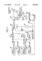
- FIG. 1 is a block diagram depicting a memory system using a frame memory and a buffer memory in accordance with the present invention
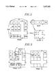
- FIG. 2 shows an exemplary image formatting structures of a frame
- FIG. 3 is depicts a block matching technique for motion estimation
- FIG. 4 is a timing diagram illustrating read/write memory cycles operating in an inventive memory system.
- FIG. 1 shows a memory system comprising a frame memory 58 and a buffer memory 62 in accordance with the present invention.
- the frame memory stores a portion of previous frame data which will be used for motion compensation of a current frame and a portion of the current frame data in the rest part of the memory.
- a FIFO (First-In First-Out) buffer memory 62 temporarily stores motion compensated current frame data and provides them to the frame memory in accordance with the invention.
- Read and write addressing for the memory 58 is performed in accordance with image formatting structures of a frame. Referring to FIG. 2, there is illustrated an exemplary frame of 720 ⁇ 320 pixels having 40 slices, each of which is formed by 90 blocks.
- a block which has, e.g., 8 ⁇ 8 pixels is a basic processing unit used, e.g., in DCT and VLC.
- memory addressing is carried out block-by-block basis.
- a pixel counter 46 generates in sequence 3 bit column address signals of AH2-AH0 in response to the clock signals via line from a clock 68. Those 3 bit address signals are used for addressing sequentially 8 pixels in a row of a block.
- carries are generated by the pixel counter 46 and provided to a line counter 42 through a line 2.
- 3 bit 8 row address signals AV2-AV0 of the pixels in the block are generated from the line counter 42.
- the column address signals of AH2-AH0 and the row address signals of AV2-AV0 define all 8 ⁇ 8 pixels of a block. Carries are then generated from the line counter 42 in every 8 row address signals to feed to a block counter 44 via a line 3.
- a carry is generated from the block counter 44 and fed to a slice counter 40 which generates 6 bit row address signals of AV8-AV3 to, thereby, designate next slice positions until the frame is filled by, e.g., 40 slices as shown in FIG. 2.
- the process is carried out repeatedly by resetting the counters 40, 42, 44 and 46 for every frame.
- the row address signal AV2-AV0 from the line counter 42 and AV8-AV3 from the slice counter 40 is combined to form 9 bit column signal AV8-AV0 and fed to a first adder 48 wherein the vertical component MVV of a respective motion vector of a pixel from, e.g., a variable length decoder (not shown) are added thereto.
- a first adder 48 wherein the vertical component MVV of a respective motion vector of a pixel from, e.g., a variable length decoder (not shown) are added thereto.
- the combined 10 bit column address signal AH9-AH0 composed of 3 bit column signal AH2-AH0 from the pixel counter 46 and 7 bit column signal AH9-AH3 from the block counter 44 are summed up with the horizontal component MVH of the respective motion vector of the pixel in the second adder 50.
- the 19 bit address signal from the first second address 48 and 50 are provided to a first multiplexer 56 as a read address RA18-RA0 which is used for designating a previous frame pixel data stored in the frame memory 58 for the motion compensation.
- the column address signal AH9-AH0 and the row address signal AV8-AV0 are fed through a line 5 to a T s delay unit 52 and on offset unit 54.
- a block matching technique which sums the mean square difference (or similar function) between each pixel of corresponding blocks in adjacent frames. This calculation is performed with a range of different spatial offsets between the blocks and the offset that gives the minimum error is taken as the motion vector for that block.
- a motion search range is from -8 to +8 pixels in both the vertical and horizontal directions
- the block matching of a block 91 in a frame f n is performed in a motion search range of its previous frame f n-1 .
- a motion vector V and its vertical and horizontal components V y and V x for a matched block A in the frame f n-1 of the frame 91 in the frame f n .
- pixel data of a first slice formed by blocks 0-89 and a block 90 of a previous frame stored a memory, e.g., frame memory 58 in FIG. 1 cannot be replaced with motion compensated pixel data of a current frame: for those blocks are within motion search range of following blocks, e.g., of 91 to 179, of the current frame.
- 19 bit address signal including AV8-AV0 and AH9-AH0 is fed to the T s delay unit 52 and the offset unit 54 via line 5.
- the 19 bit address signal is delayed by a delay time T s , which represents time for processing pixels in one slice and one block, and applied to the first multiplexer 56 as write address signal WA18-WA0.
- the offset unit compares the input address signal with an offset address, which is defined herein as an address of the first pixel position of the block 91 (that is, the pixel on the top-left corner thereof).
- the offset unit 54 generate "0" when the input address falls within the offset address, i.e., the input address corresponds to one of pixel positions in the blocks of 0 to 90 in FIG. 2, and generates "1" otherwise.
- An output signal of either “0” or “1” are fed to an AND gate 60 together with the clock signal from the clock 68 and to a selection terminal S1 of a second multiplexer 66 having two input terminals for logic "0" and the clock signal.
- the AND gate 60 outputs "0" to a selection terminal S0 of the first multiplexer 56, thereby enabling the first multiplexer 56 to dispatch the read address signal RA18-RA0 as an output signal A18-A0 to the frame memory 58.
- the output signal "0" from the offset unit 54 is fed to a second multiplexer 66 which select the logic "0" as an output.
- the output signal "0” is applied to a control terminal R/W of the frame memory 58 thereby enabling the input signal A18-A0 thereto to perform read operation; and to a control terminal R/W of a FIFO buffer memory 62 via a inverter 64, which converts output signal "0" from the second multiplexer 66 into "1", thereby enabling writing operation onto the FIFO buffer memory 62.
- the frame memory 58 is in a read mode and the FIFO buffer memory 62 is in a write mode.
- previous pixel data is read from the frame memory 58 to a third adder 70 and added up with pixel difference signals, e.g., from an inverse DCT unit (not shown), to constitute pixel data of the current frame.
- the output from the third adder 70 is transferred therefrom for display and to the FIFO buffer memory 62 and written thereon.
- pixel signals of the first one slice and a next block, i.e., from block 0 to 90, of the current frame is written onto the FIFO buffer memory 62 and does not replace corresponding pixels in the frame memory 58 as shown in FIG. 4, wherein a) illustrates blocks of the previous frame read from the frame memory 58; b), blocks of the current frame written onto the FIFO frame memory 62; and c), blocks of the current frame written onto the frame memory 58, which are all drawn as a function of time.
- the offset unit 54 When the input address signal to the offset unit 54 corresponds to the pixel positions outside of one slice and one block, i.e., belongs to blocks from 91 to 3599 in FIG. 2, the offset unit 54 provides "1" to the AND gate 60 and the second multiplexer 66 thereby causing both of them to generate signal "0" and "1" alternatively.
- write address signal delayed by T s in the T s delay unit 52 is selected as the output A18-A0 by the first multiplexer 56 and fed to the frame memory 58 and writing mode is actuated therein by the signal "1" from the second multiplexer 66 thereby replacing with a pixel data of the current frame from the FIFO buffer memory 62 one pixel data of the previous frame at the address designated by the write address signal from the first multiplexer 56.
- a read address signal RA18-RA0 is selected by the first multiplexer 56 and applied to the frame memory 58 wherein a pixel data corresponding to the read address signal is read and transferred to the third adder 70.
- a input pixel difference signal is summed up with the pixel data from the frame memory 58 and transferred to a display unit (not shown) and the FIFO buffer memory 62 and written therein by the inverted signal "1" from the inverter 64.
- the read/write process is repeated continuously up to the end of the frame as shown in FIG. 4.
- an inventive memory system with a reduced memory size for use in a receiver for decoding digitized video signals.
Landscapes
- Engineering & Computer Science (AREA)
- Multimedia (AREA)
- Signal Processing (AREA)
- Microelectronics & Electronic Packaging (AREA)
- Computer Vision & Pattern Recognition (AREA)
- Physics & Mathematics (AREA)
- General Physics & Mathematics (AREA)
- Theoretical Computer Science (AREA)
- Compression Or Coding Systems Of Tv Signals (AREA)
Abstract
Description
Claims (1)
Applications Claiming Priority (2)
| Application Number | Priority Date | Filing Date | Title |
|---|---|---|---|
| KR1992-18396 | 1992-10-07 | ||
| KR1019920018396A KR0129557B1 (en) | 1992-10-07 | 1992-10-07 | Memory apparatus in a motion picture data processor using a motion compensation |
Publications (1)
| Publication Number | Publication Date |
|---|---|
| US5457481A true US5457481A (en) | 1995-10-10 |
Family
ID=19340760
Family Applications (1)
| Application Number | Title | Priority Date | Filing Date |
|---|---|---|---|
| US08/133,622 Expired - Lifetime US5457481A (en) | 1992-10-07 | 1993-10-07 | Memory system for use in a moving image decoding processor employing motion compensation technique |
Country Status (3)
| Country | Link |
|---|---|
| US (1) | US5457481A (en) |
| JP (1) | JP3522801B2 (en) |
| KR (1) | KR0129557B1 (en) |
Cited By (13)
| Publication number | Priority date | Publication date | Assignee | Title |
|---|---|---|---|---|
| US5619282A (en) * | 1994-06-13 | 1997-04-08 | Lg Electronics Inc. | Image motion compensating address generator |
| US5696698A (en) * | 1994-04-27 | 1997-12-09 | Sgs-Thomson Microelectronics S.A. | Device for addressing a cache memory of a compressing motion picture circuit |
| US5907500A (en) * | 1996-10-21 | 1999-05-25 | Nec Corporation | Motion compensation adder for decoding/decompressing compressed moving pictures |
| US6128340A (en) * | 1997-03-14 | 2000-10-03 | Sony Corporation | Decoder system with 2.53 frame display buffer |
| SG81239A1 (en) * | 1997-07-30 | 2001-06-19 | Sony Corp | Storage device and access method |
| US20020180676A1 (en) * | 2001-05-11 | 2002-12-05 | Lee Baek-Woon | Liquid crystal display and method of modifying gray signals for the same |
| US20030106053A1 (en) * | 2001-12-04 | 2003-06-05 | Sih Gilbert C. | Processing digital video data |
| US20040190632A1 (en) * | 2003-03-03 | 2004-09-30 | Cismas Sorin C. | Memory word array organization and prediction combination for memory access |
| US20060114358A1 (en) * | 2004-12-01 | 2006-06-01 | Silverstein D Amnon | Artifact reduction in a digital video |
| US20130207981A1 (en) * | 2012-02-09 | 2013-08-15 | Honeywell International Inc. | Apparatus and methods for cursor animation |
| TWI408620B (en) * | 2008-12-12 | 2013-09-11 | Mstar Semiconductor Inc | Image processing method for determining motion vectors of interpolated picture and related apparatus thereof |
| US20140218767A1 (en) * | 2013-02-01 | 2014-08-07 | Canon Kabushiki Kaisha | Image forming apparatus, memory management method for image forming apparatus, and program |
| CN107666621A (en) * | 2017-09-28 | 2018-02-06 | 惠州Tcl移动通信有限公司 | Mobile terminal and video pictures output intent and storage medium |
Families Citing this family (3)
| Publication number | Priority date | Publication date | Assignee | Title |
|---|---|---|---|---|
| JP3861607B2 (en) | 2001-02-22 | 2006-12-20 | セイコーエプソン株式会社 | Image signal decoding apparatus |
| WO2007020560A1 (en) | 2005-08-17 | 2007-02-22 | Nxp B.V. | Method video encoding and decoding preserving cahe localities |
| KR100836534B1 (en) * | 2006-12-01 | 2008-06-10 | 한국과학기술원 | A low power sub-pixel interpolator architecture |
Citations (5)
| Publication number | Priority date | Publication date | Assignee | Title |
|---|---|---|---|---|
| US4445115A (en) * | 1980-09-29 | 1984-04-24 | Asea Aktiebolag | Display control unit having means for symbolic representation of graphical symbols |
| US4691230A (en) * | 1985-03-04 | 1987-09-01 | Kokusai Denshin Denwa Co., Ltd. | Motion vector detection system of a moving object on a screen |
| US5089887A (en) * | 1988-09-23 | 1992-02-18 | Thomson Consumer Electronics | Method and device for the estimation of motion in a sequence of moving images |
| US5121202A (en) * | 1989-05-12 | 1992-06-09 | Nec Corporation | Adaptive interframe prediction coded video communications system |
| US5204740A (en) * | 1989-01-14 | 1993-04-20 | Canon Kabushiki Kaisha | Image signal decoding apparatus |
-
1992
- 1992-10-07 KR KR1019920018396A patent/KR0129557B1/en not_active IP Right Cessation
-
1993
- 1993-10-07 US US08/133,622 patent/US5457481A/en not_active Expired - Lifetime
- 1993-10-07 JP JP25200593A patent/JP3522801B2/en not_active Expired - Lifetime
Patent Citations (5)
| Publication number | Priority date | Publication date | Assignee | Title |
|---|---|---|---|---|
| US4445115A (en) * | 1980-09-29 | 1984-04-24 | Asea Aktiebolag | Display control unit having means for symbolic representation of graphical symbols |
| US4691230A (en) * | 1985-03-04 | 1987-09-01 | Kokusai Denshin Denwa Co., Ltd. | Motion vector detection system of a moving object on a screen |
| US5089887A (en) * | 1988-09-23 | 1992-02-18 | Thomson Consumer Electronics | Method and device for the estimation of motion in a sequence of moving images |
| US5204740A (en) * | 1989-01-14 | 1993-04-20 | Canon Kabushiki Kaisha | Image signal decoding apparatus |
| US5121202A (en) * | 1989-05-12 | 1992-06-09 | Nec Corporation | Adaptive interframe prediction coded video communications system |
Cited By (20)
| Publication number | Priority date | Publication date | Assignee | Title |
|---|---|---|---|---|
| US5696698A (en) * | 1994-04-27 | 1997-12-09 | Sgs-Thomson Microelectronics S.A. | Device for addressing a cache memory of a compressing motion picture circuit |
| USRE38720E1 (en) | 1994-06-13 | 2005-04-12 | Lg Electronics, Inc. | Image motion compensating address generator |
| US5619282A (en) * | 1994-06-13 | 1997-04-08 | Lg Electronics Inc. | Image motion compensating address generator |
| US5907500A (en) * | 1996-10-21 | 1999-05-25 | Nec Corporation | Motion compensation adder for decoding/decompressing compressed moving pictures |
| US6128340A (en) * | 1997-03-14 | 2000-10-03 | Sony Corporation | Decoder system with 2.53 frame display buffer |
| SG81239A1 (en) * | 1997-07-30 | 2001-06-19 | Sony Corp | Storage device and access method |
| US7884793B2 (en) * | 2001-05-11 | 2011-02-08 | Samsung Electronics Co., Ltd. | Liquid crystal display and method of modifying gray signals for the same |
| US20020180676A1 (en) * | 2001-05-11 | 2002-12-05 | Lee Baek-Woon | Liquid crystal display and method of modifying gray signals for the same |
| US20030106053A1 (en) * | 2001-12-04 | 2003-06-05 | Sih Gilbert C. | Processing digital video data |
| WO2003049454A3 (en) * | 2001-12-04 | 2003-09-04 | Qualcomm Inc | Processing digital video data |
| US7236177B2 (en) | 2001-12-04 | 2007-06-26 | Qualcomm Incorporated | Processing digital video data |
| US20040190632A1 (en) * | 2003-03-03 | 2004-09-30 | Cismas Sorin C. | Memory word array organization and prediction combination for memory access |
| US20060114358A1 (en) * | 2004-12-01 | 2006-06-01 | Silverstein D Amnon | Artifact reduction in a digital video |
| US7643088B2 (en) * | 2004-12-01 | 2010-01-05 | Hewlett-Packard Development Company, L.P. | Artifact reduction in a digital video |
| TWI408620B (en) * | 2008-12-12 | 2013-09-11 | Mstar Semiconductor Inc | Image processing method for determining motion vectors of interpolated picture and related apparatus thereof |
| US8774276B2 (en) | 2008-12-12 | 2014-07-08 | Mstar Semiconductor, Inc. | Image processing method for determining motion vectors of interpolated picture and related apparatus |
| US20130207981A1 (en) * | 2012-02-09 | 2013-08-15 | Honeywell International Inc. | Apparatus and methods for cursor animation |
| US20140218767A1 (en) * | 2013-02-01 | 2014-08-07 | Canon Kabushiki Kaisha | Image forming apparatus, memory management method for image forming apparatus, and program |
| US9948809B2 (en) * | 2013-02-01 | 2018-04-17 | Canon Kabushiki Kaisha | Image forming apparatus, memory management method for image forming apparatus, and program, using discretely arranged blocks in prioritizing information |
| CN107666621A (en) * | 2017-09-28 | 2018-02-06 | 惠州Tcl移动通信有限公司 | Mobile terminal and video pictures output intent and storage medium |
Also Published As
| Publication number | Publication date |
|---|---|
| JPH06205395A (en) | 1994-07-22 |
| KR940010780A (en) | 1994-05-26 |
| KR0129557B1 (en) | 1998-04-10 |
| JP3522801B2 (en) | 2004-04-26 |
Similar Documents
| Publication | Publication Date | Title |
|---|---|---|
| US5650782A (en) | Variable length coder using two VLC tables | |
| US5473379A (en) | Method and apparatus for improving motion compensation in digital video coding | |
| US6151075A (en) | Device and method for converting frame rate | |
| US5457481A (en) | Memory system for use in a moving image decoding processor employing motion compensation technique | |
| US5657087A (en) | Motion compensation encoding method and apparatus adaptive to motion amount | |
| EP0720374A1 (en) | Apparatus for parallel decoding of digital video signals | |
| US5134480A (en) | Time-recursive deinterlace processing for television-type signals | |
| US6990241B2 (en) | Circuit and method for decoding an encoded version of an image having a first resolution directly into a decoded version of the image having a second resolution | |
| CA2060380C (en) | Method and apparatus for communicating compressed digital video signals using multiple processors | |
| KR100239260B1 (en) | Picture decoder | |
| US5583580A (en) | Method and apparatus for detecting motion vectors based on hierarchical motion estimation | |
| US5835148A (en) | Apparatus for parallel decoding of digital video signals | |
| US4488175A (en) | DPCM Video signal processing technique with spatial subsampling | |
| EP0785682A1 (en) | Letter box converter | |
| EP0714208B1 (en) | Method and system for decoding coded video signals | |
| EP0840519B1 (en) | Apparatus and method of coding/decoding moving pictures | |
| JP2898413B2 (en) | Method for decoding and encoding compressed video data streams with reduced memory requirements | |
| US5521642A (en) | Decoding system for compact high definition television receivers | |
| JP2947389B2 (en) | Image processing memory integrated circuit | |
| US6061401A (en) | Method and apparatus for selectively encoding/decoding a video signal | |
| EP0720372A1 (en) | Apparatus for parallel encoding/decoding of digital video signals | |
| JPH0363275B2 (en) | ||
| KR100240620B1 (en) | Method and apparatus to form symmetric search windows for bidirectional half pel motion estimation | |
| US5774677A (en) | Dual interleaved block motion compensation | |
| JPH0622291A (en) | Decoding method and device capable of resolution conversion |
Legal Events
| Date | Code | Title | Description |
|---|---|---|---|
| AS | Assignment |
Owner name: DAEWOO ELECTRONICS CO., LTD., KOREA, REPUBLIC OF Free format text: ASSIGNMENT OF ASSIGNORS INTEREST;ASSIGNORS:SOHN, CHANG;KWON, OH-SANG;REEL/FRAME:006720/0925 Effective date: 19930927 |
|
| STCF | Information on status: patent grant |
Free format text: PATENTED CASE |
|
| FEPP | Fee payment procedure |
Free format text: PAYOR NUMBER ASSIGNED (ORIGINAL EVENT CODE: ASPN); ENTITY STATUS OF PATENT OWNER: LARGE ENTITY |
|
| FPAY | Fee payment |
Year of fee payment: 4 |
|
| FPAY | Fee payment |
Year of fee payment: 8 |
|
| AS | Assignment |
Owner name: DAEWOO ELECTRONICS CORPORATION, KOREA, REPUBLIC OF Free format text: ASSIGNMENT OF ASSIGNORS INTEREST;ASSIGNOR:DAEWOO ELECTRONICS CO., LTD.;REEL/FRAME:013645/0159 Effective date: 20021231 |
|
| FPAY | Fee payment |
Year of fee payment: 12 |
|
| AS | Assignment |
Owner name: MAPLE VISION TECHNOLOGIES INC., CANADA Free format text: ASSIGNMENT OF ASSIGNORS INTEREST;ASSIGNOR:DAEWOO ELECTRONICS CORPORATION;REEL/FRAME:027437/0345 Effective date: 20111215 |
|
| AS | Assignment |
Owner name: QUARTERHILL INC., CANADA Free format text: MERGER AND CHANGE OF NAME;ASSIGNORS:MAPLE VISION TECHNOLOGIES INC.;QUARTERHILL INC.;REEL/FRAME:042935/0282 Effective date: 20170601 |
|
| AS | Assignment |
Owner name: WI-LAN INC., CANADA Free format text: ASSIGNMENT OF ASSIGNORS INTEREST;ASSIGNOR:QUARTERHILL INC.;REEL/FRAME:043182/0859 Effective date: 20170601 |