US5453661A - Thin film ferroelectric flat panel display devices, and methods for operating and fabricating same - Google Patents
Thin film ferroelectric flat panel display devices, and methods for operating and fabricating same Download PDFInfo
- Publication number
- US5453661A US5453661A US08/228,116 US22811694A US5453661A US 5453661 A US5453661 A US 5453661A US 22811694 A US22811694 A US 22811694A US 5453661 A US5453661 A US 5453661A
- Authority
- US
- United States
- Prior art keywords
- thin film
- electrode
- flat panel
- panel display
- ferroelectric thin
- Prior art date
- Legal status (The legal status is an assumption and is not a legal conclusion. Google has not performed a legal analysis and makes no representation as to the accuracy of the status listed.)
- Expired - Fee Related
Links
Images


Classifications
-
- H—ELECTRICITY
- H01—ELECTRIC ELEMENTS
- H01J—ELECTRIC DISCHARGE TUBES OR DISCHARGE LAMPS
- H01J63/00—Cathode-ray or electron-stream lamps
-
- B—PERFORMING OPERATIONS; TRANSPORTING
- B82—NANOTECHNOLOGY
- B82Y—SPECIFIC USES OR APPLICATIONS OF NANOSTRUCTURES; MEASUREMENT OR ANALYSIS OF NANOSTRUCTURES; MANUFACTURE OR TREATMENT OF NANOSTRUCTURES
- B82Y10/00—Nanotechnology for information processing, storage or transmission, e.g. quantum computing or single electron logic
-
- H—ELECTRICITY
- H01—ELECTRIC ELEMENTS
- H01J—ELECTRIC DISCHARGE TUBES OR DISCHARGE LAMPS
- H01J1/00—Details of electrodes, of magnetic control means, of screens, or of the mounting or spacing thereof, common to two or more basic types of discharge tubes or lamps
- H01J1/02—Main electrodes
- H01J1/30—Cold cathodes, e.g. field-emissive cathode
- H01J1/312—Cold cathodes, e.g. field-emissive cathode having an electric field perpendicular to the surface, e.g. tunnel-effect cathodes of Metal-Insulator-Metal [MIM] type
-
- H—ELECTRICITY
- H01—ELECTRIC ELEMENTS
- H01J—ELECTRIC DISCHARGE TUBES OR DISCHARGE LAMPS
- H01J2201/00—Electrodes common to discharge tubes
- H01J2201/30—Cold cathodes
- H01J2201/306—Ferroelectric cathodes
-
- H—ELECTRICITY
- H01—ELECTRIC ELEMENTS
- H01J—ELECTRIC DISCHARGE TUBES OR DISCHARGE LAMPS
- H01J2329/00—Electron emission display panels, e.g. field emission display panels
Definitions
- This invention relates to display devices and more particularly to solid state display devices.
- the cathode ray tube is the predominant display device for electronic systems such as computers and televisions, notwithstanding its many shortcomings. Among these shortcomings are the large spatial volume (footprint) occupied by a CRT, the high power supply voltages needed for the tube and the relatively short lifetime of the tube.
- Flat panel displays include light emitting diode displays, liquid crystal displays, field emitter displays, and electroluminescent displays.
- flat panel displays have their own limitations which prevent replacing a CRT for many applications.
- a field emitter display typically includes an array of field emission tips which emit electrons upon application of appropriate voltages thereto. The emitted electrons are caused to strike a luminescent material such as a phosphor to create a display.
- a luminescent material such as a phosphor
- field emitter displays typically require tens to hundreds of volts for electron emission, which makes it difficult to use these displays in many applications.
- the electron emission tips also typically need to be surrounded by a very high vacuum at least 10 -5 Torr and often as high as 10 -8 -10 9 Torr in order to prevent degradation of the tips. Such high vacuums are difficult to maintain in the small volume enclosing the emitters.
- Electroluminescent displays are formed by applying an electric field across a luminescent material, typically a phosphor, in sufficient magnitude to cause avalanche breakdown of the phosphor.
- the light generated by recombination of electron-hole pairs produced by the breakdown can be tuned in wavelength by the addition of various impurity ions to the phosphor.
- a history and survey of electroluminescent displays is described in Chapter 8 of Flat-Panel Displays and CRTs, edited by L. E. Tannas, Jr., Van Nostrand Reinhold Publisher, New York, 1985, entitled Electroluminescent Displays by L. E. Tannas, Jr., pp. 237-284.
- the luminescent (phosphor) layer is typically surrounded by dielectric layers such as amorphous thin film of, for example, aluminum oxide.
- ferroelectric materials can emit electrons.
- ferroelectric materials are polar dielectrics that undergo a change of spontaneous polarization under the influence of an applied electric field.
- bulk ferroelectric materials of about 1 mm in thickness as an electron emitter. See for example Time-Dependent Electron Emission From Ferroelectrics by External Pulsed Electric Fields, H. Gundel et al., J. Appl. Phys. 69(2), 15 Jan. 1991, pp. 975-982; Pulsed Emission Characteristics of Ferroelectric Cathodes Under Two Exciting Modes, Z.
- a flat panel display which includes a ferroelectric thin film between first and second spaced apart electrodes.
- the ferroelectric thin film emits electrons upon application of a predetermined voltage between the first and second spaced apart electrodes.
- the electrons are emitted in an electron emission path and impinge upon a luminescent layer, such as a phosphor layer, which produces luminescence upon impingement of the emitted electrons thereon.
- the ferroelectric thin film is preferably about 2 ⁇ m or less in thickness and is preferably a polycrystalline ferroelectric thin film. More preferably, the thin ferroelectric film is a highly oriented polycrystalline thin ferroelectric film. Most preferably, the highly oriented ferroelectric thin film has a (001) crystal orientation, and is about 2 ⁇ m or less in thickness. In this configuration, the predetermined voltage for causing electron emission is about 50 volts or less.
- a thin film ferroelectric display also includes a third electrode adjacent to the phosphor layer.
- the third electrode accelerates the emitted electrons from the ferroelectric thin film to the phosphor layer.
- the phosphor layer may be placed directly on the thin film ferroelectric layer in which case electrons originating at the ferroelectric/phosphor layer interface would be injected directly into the phosphor layer.
- the phosphor layer may be spaced apart from the thin ferroelectric film to define a gap therebetween, and emitted electrons may be injected across the gap into the phosphor layer.
- an array of thin film ferroelectric display elements are used to form a flat panel display.
- the flat panel display includes first and second electrode arrays, which are spaced apart from one another to define an array of electrode pairs such that the electrode pairs produce an electric field therebetween upon application of a predetermined voltage therebetween.
- the flat panel display also includes a ferroelectric thin film between each of the electrode pairs, such that the ferroelectric thin film emits electrons therefrom in an electron emission path for each electrode pair, upon application of the predetermined voltage between the electrode pair.
- a luminescent layer is present in the electron emission path of each electrode pair.
- the electrodes in the first and second arrays may extend in a direction along the respective first and second arrays to form top and bottom electrode pairs.
- the electrodes in the second electrode array may be patterned electrodes so that the electron emission path from each electrode pair passes through the corresponding patterned second electrode.
- each of the electrodes in the first and second arrays may extend in a direction transverse to the respective first and second arrays, to form side electrode pairs. In this case, the electron emission path from each electrode pair is transverse to the first and second electrodes of the corresponding electrode pair.
- a thin film ferroelectric display according to the present invention may be operated using low voltages which are typically used in computer and electronic systems. Moreover, a thin film ferroelectric display according to the invention can tolerate lower vacuums, on the order of about 10 -2 -10 -3 Torr, between the ferroelectric thin film and a spaced apart luminescent (phosphor) layer. High vacuums are not required.
- a thin film ferroelectric display according to the present invention can also operate above room temperature (up to about 100° C.) and is resistant to physical deterioration due to the resistance of the ferroelectric material to chemical reaction and/or mechanical deformation.
- a visible image displaying method applies a polarization switching voltage of about 50 volts or less across a ferroelectric thin film of about 2 ⁇ m or less in thickness, to produce electron emission from the ferroelectric thin film. Electric fields of more than about 20 kV/cm may be achieved. The emitted electrons impinge onto a luminescent layer such as a phosphor to produce luminescence. A low voltage, high reliability displaying method is thereby produced.
- Flat panel displays according to the present invention may be fabricated using microelectronic fabrication steps.
- a first electrode array is formed on a substrate and a polycrystalline and preferably highly oriented ferroelectric thin film is formed on the first electrode array.
- a second electrode array is formed on the polycrystalline and preferably highly oriented ferroelectric thin film to define an electron emission path from the polycrystalline and preferably highly oriented ferroelectric thin film upon application of the predetermined voltage between the first and second electrode arrays.
- a luminescent layer is formed in the electron emission path such that the luminescent layer produces luminescence upon impingement of electrons thereon.
- the first electrode array is preferably blanket deposited on the substrate and then patterned, and the second electrode array is preferably blanket deposited and patterned on the ferroelectric layer opposite the first array.
- the ferroelectric layer may also be etched between adjacent electrodes of the second array to produce a discrete ferroelectric region for each display element.
- a first connecting electrode array is formed on the substrate and the polycrystalline and preferably highly oriented ferroelectric thin film is formed on the first connecting electrode array.
- An array of first side electrodes is formed by etching a first array of vias in the ferroelectric thin film and then filling the first vias with conductive material which electrically contacts the first connecting electrode array.
- the second electrode array may be formed by etching a second array of vias in the ferroelectric thin film, and filling the second vias with conductive material which is insulated from the first electrode array.
- a luminescent layer, and an accelerating electrode if desired are formed on a second substrate which is mounted adjacent to the ferroelectric thin film.
- the second substrate may be mounted adjacent and in direct contact with the ferroelectric thin film or may be mounted adjacent and spaced apart from the ferroelectric thin film.
- the luminescent layer may be directly deposited on the existing structure in contact with the ferroelectric layer, without using a second substrate.
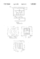
- FIG. 1 illustrates a cross-sectional view of a flat panel display according to the present invention.
- FIGS. 2A-2C illustrate top views of alternative embodiments of second electrodes according to the present invention.
- FIGS. 3A-3I illustrate cross-sectional and top views of a second embodiment of a flat panel display according to the present invention during intermediate fabrication steps.
- FIGS. 4A-4K illustrate cross-sectional and top views of a third embodiment of a flat panel display according to the present invention during intermediate fabrication steps.
- FIGS. 5A-5M illustrate cross-sectional and top views of fourth and fifth embodiments of a flat panel display according to the present invention during intermediate fabrication steps.
- Display 10 may be thought of as a single element display. More typically, however, display 10 is a single display element (pixel) of a flat panel display which includes an array of display elements. Displays which include arrays of display elements will be described below.
- flat panel display 10 includes first and second spaced apart electrodes 12 and 11 respectively, and a ferroelectric thin film 13 between the first and second spaced apart electrodes.
- First electrode 12 is preferably formed on a substrate 19.
- Ferroelectric thin film 13 is preferably a polycrystalline ferroelectric thin film, more preferably a highly oriented polycrystalline thin film, and most preferably a highly oriented polycrystalline thin film having (001) crystal orientation with respect to substrate 19.
- polycrystalline ferroelectric material includes a plurality of ferroelectric crystalline grains. In a conventional polycrystalline ferroelectric thin film, the grains are oriented randomly. In a highly oriented polycrystalline film, substantially all of the grains are oriented in the same direction.
- highly oriented polycrystalline ferroelectric thin films may be readily distinguished from randomly oriented films by X-ray diffraction, wherein the highly oriented (001) film shows one X-ray diffraction peak (001) and a randomly oriented film shows several peaks corresponding to other orientations such as (110) and (101). See an article by O. Auciello et al., entitled A Review of Composition-Structure-Property Relationships for PZT-Based Heterostructure Capacitors, Integrated Ferroelectronics, preprint, 1994.
- Other techniques for distinguishing highly oriented and randomly oriented polycrystalline ferroelectric thin films are well known to those having skill in the art.
- the substrate 19 and first electrode 12 are preferably chosen to have a crystalline structure which promotes highly oriented polycrystalline growth.
- substrate 19 may be a magnesium oxide (MgO) substrate or an MgO layer formed on a silicon or other substrate.
- First electrode 12 may be platinum or RuO 2 or combinations thereof, or other metal or conductive metal oxide.
- Ferroelectric thin film 13 may be any ferroelectric material such as lead zirconate titanate (PZT) or other well known ferroelectric materials.
- PZT lead zirconate titanate
- the fabrication of highly oriented ferroelectric thin films is well known to those having skill in the art and is described, or example, in a textbook entitled Multicomponent and Multilayer Thin Films for Advanced Microtechnologies: Techniques, Fundamentals and Devices edited by coinventor Auciello et al., published by Kluwer Academic Publishers, 1993, in a chapter entitled Physical Vapor Deposition of Multicomponent Dioxide Thin Films: Techniques, Basic Deposition Processes and Film Processing-Microstructure-Property Relationships by coinventor Auciello et al., pp.
- ferroelectric thin film 13 is about 2 ⁇ m or less in thickness. Accordingly, electrons may be emitted from the ferroelectric thin film 13 in an electron emission path 14 upon application of polarization switching voltages in the range of about 50 volts or less between electrodes 11 and 12.
- a luminescent layer 15 such as a phosphor is placed in the electron emission path 14 so that the emitted electrons impinge thereon and produce luminescence in the luminescent layer 15.
- a third electrode 16 may also be present for accelerating the electrons which are emitted from the thin film ferroelectric layer 13 into the luminescent layer 15.
- a support structure 17 maintains the luminescent layer 15 in spaced apart relation from the ferroelectric layer 13, thereby creating a gap 18 therebetween.
- the gap is preferably maintained under vacuum conditions at a pressure of less than about 10 -3 Torr. This contrasts with conventional field emitter devices which require high minus vacuums on the order of 10 -8 -10 -9 Torr.
- gap 18 is not present, and luminescent layer 15 is formed directly on ferroelectric material 13 and second electrode 11.
- the first single pixel electrode 12 is preferably a solid electrode.
- the second single pixel electrode 11 is preferably a patterned electrode as shown in FIG. 1.
- FIGS. 2A-2C illustrate top views of alternative embodiments of the second electrode 11.
- FIG. 2A illustrates a ring electrode 11a.
- FIG. 2B illustrates a spiral electrode 11b and
- FIG. 2C illustrates a finger electrode 11c.
- the patterned second electrode 11 is used to support a voltage across the ferroelectric material while allowing electron emission from those areas which are not covered by the electrode material. Since the emission area is increased, more electrons are emitted, thereby producing a brighter display.
- the ferroelectric in a steady state, the ferroelectric appears neutral to its surrounding environment because any remnant polarization is immediately compensated by free charge carriers.
- surface charge densities of about 30 ⁇ C/cm 2 or higher can exist in a normal equilibrium state without affecting the surrounding environment.
- this charge equilibrium may be disturbed for short transient time, generating a surplus of charges at opposite faces of the affected volume.
- conditions are chosen in order to achieve a surplus of negative charges at the emitting surface, resulting in electron emission.
- the electrons are drawn from energetically favorable levels in the material. These levels may be screening charges of electrons trapped by defects, or others.
- a fast change of the spontaneous polarization due to a phase shift, and/or partial reversal of the spontaneous polarization induced by the application of high electric field pulses to a ferroelectric thin film is preferably used.
- a phase shift offers the advantage that after emission the ferroelectric material relaxes back to its initial state prior to the voltage pulse. Thus, no resetting is necessary.
- Reversal inside the ferroelectric phase may require active resetting, either by applying pulses with alternating polarity, or by pulsing from a low continuous potential level to the opposite polarity.
- the emission dynamics are strongly correlated to the actual material use, taking into account the kind of phase transition (first and second order), nucleation and domain wall motion, grain properties, defect concentration, and other known factors.
- FIGS. 3A-3I a method of fabricating a second embodiment of a first flat panel display according to the invention will be described. Fabrication of a 5 ⁇ 5 array of display elements is illustrated. However, it will be understood by those having skill in the art that typically many more elements are fabricated in a single display.
- first electrode 12 is formed on a suitable substrate 19 using techniques well known to those having skill in the art.
- a thin film of platinum (or any other metal) or a multicomponent oxide material (YBaCuO, LaSrCoO, RuO 2 , or any other conducting oxide) with a perovskite or other structure similar to that of the ferroelectric thin film is deposited on an appropriate substrate 19.
- the substrate 19 can be any thin film or bulk material (such as MgO or SrTiO) or other material on which an appropriate template layer is deposited to yield suitable lattice matching and serve as a diffusion barrier to avoid possible destructive interactions between the substrate and the ferroelectric layer.
- Semiconductors e.g., Si, GaAs are possible substrate materials of the latter type.
- a diffusion barrier may be needed to avoid interdiffusion of the electrode layer 12, and the substrate 19 at the temperatures needed (400°-600° C.) to produce an epitaxial electrode layer, which has been proven to be suitable to obtain optimized polarization hysteresis loops and reduced or negligible polarization fatigue.
- oxide electrodes may be necessary to obtain electrode/ferroelectric/electrode structures that can sustain many voltage cycles without reduction of the material polarization, to produce a long lifetime electron emitter.
- first electrode 12 is patterned to form first electrode array.
- FIG. 3C illustrates a top view of the first electrode array. As illustrated, interconnected electrode columns are formed. Each column of electrodes includes an associated first contact pad 21. Thus, a column of first electrodes 12 is energized by applying an appropriate voltage to the associated first contact pad 21. As shown in FIG. 3C, each first electrode 12 is a square shape. However, other shapes may be used.
- first electrode 12 need not be patterned as shown in FIG. 2B. Rather, an unpatterned electrode layer can be formed across substrate 19.
- the bottom electrodes form a plurality of column electrodes and the top electrodes form a plurality of row electrodes, or vice versa, so that a particular display element may be energized by energizing the appropriate row and column.
- the first and second electrode arrays define an array of electrode pairs which produce an electric field therebetween upon application of a predetermined voltage therebetween.
- a thin film ferroelectric layer 13 is deposited and planarized on substrate 19 and first electrodes 12 using techniques well known to those having skill in the art.
- a ferroelectric thin film is deposited by any of the techniques currently used, i.e., sputter-or laser ablation-deposition, sol-gel, or chemical vapor deposition.
- Any ferroelectric material capable of sustaining prolonged polarization switching under AC voltage excitation can be used for this application, such as Pb(Zr x Ti 1-x ) O 3 , PbLa x (Zr y Ti 1-y )O 3 , PbTiO 3 or any other ferroelectric material.
- the second electrodes are deposited and patterned to form a second electrode array.
- FIG. 3F illustrates a top view of the second electrodes.
- the second electrodes can be patterned in different configurations, such as the configurations shown in FIGS. 2A, 2B, and 2C, or other patterns.
- the second electrodes 11a (or 11b or 11c) are patterned so as to expose a large area of ferroelectric material adjacent to the electrode material to provide increased emission.
- each row of second electrodes is connected to a second contact 22 so that excitation of the appropriate second contact pad 22 and an appropriate first contact pad 21 of FIG. 3C uniquely energizes an electrode pair, and thereby energizes a display element.
- the ferroelectric material between the adjacent electrodes in the first array is etched.
- Etching of the ferroelectric layer 13 is an optional step which may produce sharper emissions by preventing emissions between adjacent second electrodes 11a, and restricting emissions to through the second electrodes 11a, in the emission paths 14.
- the ferroelectric layer 13 need not be patterned between adjacent electrodes. Etching of the ferroelectric layer 13 typically needs to be done to expose the contact pads 21 of the first electrode 12.
- a third (accelerator) electrode 16 is deposited on a glass or other transparent second substrate 17.
- the accelerator electrode is a blanket (unpatterned) electrode.
- the accelerator electrode may be patterned in rows and/or columns in the patterns shown in FIG. 3C or 3F, or in other row and column patterns, so that only a row or column of accelerator electrodes is energized upon excitation of a selected display element.
- the third electrode 16 Upon application of an appropriate voltage to the third electrode 16 the electrons which are emitted from the ferroelectric layer are accelerated.
- a patterned third electrode 16 may be preferred for improved operation of the flat panel display because an unpatterned third electrode may divert electrons from the paths 14.
- a patterned accelerator electrode may enhance the definition of the display element by accelerating electrodes only in a direction orthogonal to the substrate 19.
- a patterned third electrode may be more difficult to align to the rest of the display.
- a luminescent layer 15 such as a phosphor is deposited on third electrode 16.
- the design and fabrication of phosphor layers are well known to those having skill in the art and need not be described further herein. Any luminescent phosphor can be used.
- the second substrate 17 is joined to substrate 19 using well known techniques. They are preferably joined under vacuum of at least 10 -3 Torr. However, atmospheric pressure, or other gas environments may be used. Accordingly, the resultant flat panel display 20 includes a plurality of display elements each of which includes a thin ferroelectric layer 13 which emits electrons onto phosphor 15 along an electron emission path 14 upon energization of appropriate row and column contacts 21 and 22.
- FIGS. 4A-4J a method for fabricating a third embodiment of a thin film ferroelectric display device according to the invention is disclosed.
- This embodiment differs from that shown in FIGS. 3A-3I, among other reasons, because the phosphor layer 15 is formed directly upon the second electrodes and on the ferroelectric layer 13, rather than being formed on a second substrate. Moreover, the ferroelectric layer is not patterned.
- a first electrode 12 is formed on substrate 19 as was described in connection with FIG. 3A.
- the substrate 19 includes a silicon or other substrate 19a and a buffer layer 19b such as MgO upon which a first electrode 12 is formed.
- FIGS. 4B-4F illustrate similar operations to those described in FIGS. 3B-3F and need not be described further.
- a phosphor layer 15 is deposited directly on second electrodes 11a and on top of ferroelectric layer 13, and is planarized if necessary.
- a third (accelerator) electrode 16 is deposited and patterned.
- FIG. 4I illustrates a top view of the patterned third (accelerator) electrode including third contact pads 23 which allow rows of accelerator electrodes to be selected.
- a contact pad 23 is energized at the same time a contact pad 22 (FIG. 4F) is energized.
- an unpatterned accelerator electrode 16 may also be provided.
- the phosphor is etched outside the second electrodes 11a in order to improve pixel definition.
- the ferroelectric layer 13 is not etched to create individual regions. However, it will be understood that ferroelectric layer etching may take place as was described in connection with FIG. 3G.
- FIG. 4K a transparent glass layer or other encapsulating layer 24 is then deposited. Accordingly, the method of FIGS. 4A-4K is highly integrated because all of the layers are formed on a single substrate.
- the device 30 of FIG. 4K also does not require a vacuum.
- FIGS. 5A-5M a method for fabricating fourth and fifth embodiments of a thin film ferroelectric display according to the present invention will now be described. The beginning steps for both embodiments are the same, but they end with different steps as will be described below.
- the first and second electrodes 12 and 11 are on the sides of the thin film ferroelectric layer, relative to the substrate on which the thin film ferroelectric display is built. Thus, they extend in a direction which is transverse to the respective first and second electrode arrays.
- the first and second electrodes 12 and 11 of FIGS. 3 and 4 may be regarded as top and bottom electrodes relative to the substrate. Thus, they extend in a direction which is along the respective first and second electrode arrays. Accordingly, in the devices produced according to the method of FIG. 5, electron emission does not need to pass through the second electrode so that the second electrode may be solid (unpatterned).
- the emission of electrons in a ferroelectric device, in a direction which is parallel to the electrodes, is described in the above identified Zang En-guan et al. article and is referred to therein as E ⁇ P emission.
- FIG. 5A an array of connecting electrodes 26 is formed on substrate 19.
- FIG. 5B illustrates a top view of the connecting electrodes 26. As shown, each connecting electrode includes a contact pad 21. Connecting electrodes 26 will subsequently be used to electrically connect the first electrodes. Thus, the formation of the array of connecting electrodes 36 may be regarded as a beginning of a step of forming the first electrode array.
- an insulating layer 27 is deposited on substrate 19 and connecting electrodes 26.
- a layer of MgO may be formed.
- Insulating layer 27 serves two primary purposes. First, it insulates second electrodes 11 from the connecting electrode 26 as will be seen in FIG. 5J below. Second, it is a substrate for subsequent growth of ferroelectric thin film 13 which is deposited thereon.
- first vias 28 are etched or otherwise formed in ferroelectric layer 13, extending through insulating layer 27. As shown in FIG. 5E, the first vias 28 are filled with first electrode material 12, and as shown in FIG. 5F, the excess electrode material is back etched.
- FIG. 5G illustrates a top view of the connecting electrodes 26, contact pads 21 and the first electrodes 12.
- FIG. 5H illustrates a top view of second electrodes 11 including second contacts 22.
- device 40 may be formed by forming a third electrode 16 and phosphor layer 15 on a second substrate 17 as was illustrated in FIG. 3H, and then joining second substrate 17 to the thin film ferroelectric device as was shown in FIG. 3I.
- device 50 of FIG. 5M may be formed by depositing phosphor layer 15 on the first and second electrodes, forming and patterning the third electrode 16 and encapsulating the resulting device using an encapsulating layer 24 as was described in connection with FIGS. 4G-4K.
Abstract
Description
Claims (41)
Priority Applications (1)
| Application Number | Priority Date | Filing Date | Title |
|---|---|---|---|
| US08/228,116 US5453661A (en) | 1994-04-15 | 1994-04-15 | Thin film ferroelectric flat panel display devices, and methods for operating and fabricating same |
Applications Claiming Priority (1)
| Application Number | Priority Date | Filing Date | Title |
|---|---|---|---|
| US08/228,116 US5453661A (en) | 1994-04-15 | 1994-04-15 | Thin film ferroelectric flat panel display devices, and methods for operating and fabricating same |
Publications (1)
| Publication Number | Publication Date |
|---|---|
| US5453661A true US5453661A (en) | 1995-09-26 |
Family
ID=22855861
Family Applications (1)
| Application Number | Title | Priority Date | Filing Date |
|---|---|---|---|
| US08/228,116 Expired - Fee Related US5453661A (en) | 1994-04-15 | 1994-04-15 | Thin film ferroelectric flat panel display devices, and methods for operating and fabricating same |
Country Status (1)
| Country | Link |
|---|---|
| US (1) | US5453661A (en) |
Cited By (58)
| Publication number | Priority date | Publication date | Assignee | Title |
|---|---|---|---|---|
| US5593495A (en) * | 1994-06-16 | 1997-01-14 | Sharp Kabushiki Kaisha | Method for manufacturing thin film of composite metal-oxide dielectric |
| US5621274A (en) * | 1996-02-27 | 1997-04-15 | Durel Corporation | Laminated EL display |
| US5663556A (en) * | 1995-03-02 | 1997-09-02 | Northwestern University | Optoelectronic ferroelectric sensor and signal generating device |
| EP0797233A2 (en) * | 1996-03-22 | 1997-09-24 | Hitachi, Ltd. | Thin-film electron emitter device and application equipment using the same |
| US5747926A (en) * | 1995-03-10 | 1998-05-05 | Kabushiki Kaisha Toshiba | Ferroelectric cold cathode |
| US5874802A (en) * | 1995-12-29 | 1999-02-23 | Samsung Display Devices Co., Ltd. | Cathode body, electron gun, and cathode ray tube employing a ferroelectric emitter |
| US5943111A (en) * | 1998-06-09 | 1999-08-24 | Symetrix Corporation | Layered superlattice ferroelectric liquid crystal display |
| FR2789223A1 (en) * | 1999-01-29 | 2000-08-04 | Univ Nantes | Electron emissive ferroelectric cathode for an electron tube, flat display screen or particle accelerator has electrodes positioned to provide a main electric field line component parallel to the electron emissive surface |
| FR2789221A1 (en) * | 1999-01-29 | 2000-08-04 | Univ Nantes | Electron emissive ferroelectric cathode for an electron tube, flat display screen or particle accelerator has supplementary ferroelectric, anti-ferroelectric or dielectric layer covering electrode portion edges |
| US6198225B1 (en) * | 1999-06-07 | 2001-03-06 | Symetrix Corporation | Ferroelectric flat panel displays |
| US20010051436A1 (en) * | 1999-12-27 | 2001-12-13 | Kim Hong Koo | Fabrication method and structure for ferroelectric nonvolatile memory field effect transistor |
| US20020153827A1 (en) * | 2000-12-22 | 2002-10-24 | Ngk Insulators, Ltd. | Electron-emitting device and field emission display using the same |
| US20030089900A1 (en) * | 2001-04-30 | 2003-05-15 | Zhizhang Chen | Tunneling emitter with nanohole openings |
| US20030098656A1 (en) * | 2000-12-22 | 2003-05-29 | Ngk Insulators, Ltd. | Electron-emitting element and field emission display using the same |
| US20040066133A1 (en) * | 2002-09-30 | 2004-04-08 | Ngk Insulators, Ltd. | Light-emitting device and field emission display having such light-emitting devices |
| US20040090398A1 (en) * | 2002-11-05 | 2004-05-13 | Ngk Insulators, Ltd. | Display |
| US20040100200A1 (en) * | 2002-02-26 | 2004-05-27 | Ngk Insulators, Ltd. | Electron emitter, method of driving electron emitter, display and method of driving display |
| EP1424715A1 (en) * | 2002-11-29 | 2004-06-02 | Ngk Insulators, Ltd. | Electron emitter |
| EP1424718A1 (en) * | 2002-11-29 | 2004-06-02 | Ngk Insulators, Ltd. | Electron emitter and light emission element |
| EP1424716A1 (en) * | 2002-11-29 | 2004-06-02 | Ngk Insulators, Ltd. | Electron emitting method of electron emitter |
| EP1424714A1 (en) * | 2002-11-29 | 2004-06-02 | Ngk Insulators, Ltd. | Electron emitter |
| EP1424717A1 (en) * | 2002-11-29 | 2004-06-02 | Ngk Insulators, Ltd. | Electronic pulse generation device |
| US20040104690A1 (en) * | 2002-11-29 | 2004-06-03 | Ngk Insulators, Ltd. | Electron emitter |
| US20040104684A1 (en) * | 2002-11-29 | 2004-06-03 | Ngk Insulators, Ltd. | Electron emitter |
| US20040104689A1 (en) * | 2002-11-29 | 2004-06-03 | Ngk Insulators, Ltd. | Electron emitting method of electron emitter |
| US20040189548A1 (en) * | 2003-03-26 | 2004-09-30 | Ngk Insulators, Ltd. | Circuit element, signal processing circuit, control device, display device, method of driving display device, method of driving circuit element, and method of driving control device |
| US20040233136A1 (en) * | 2003-03-26 | 2004-11-25 | Ngk Insulators, Ltd. | Display apparatus, method of driving display apparatus, electron emitter, method of driving electron emitter, apparatus for driving electron emitter, electron emission apparatus, and method of driving electron emisssion apparatus |
| US20040256995A1 (en) * | 2003-03-26 | 2004-12-23 | Ngk Insulators, Ltd. | Display and method for driving display |
| US20050003237A1 (en) * | 2003-07-01 | 2005-01-06 | Lg Electronics Inc. | Composition of plasma display panel |
| US20050040750A1 (en) * | 2003-08-22 | 2005-02-24 | Ngk Insulators, Ltd. | Light source |
| US6866678B2 (en) | 2002-12-10 | 2005-03-15 | Interbational Technology Center | Phototherapeutic treatment methods and apparatus |
| US20050057175A1 (en) * | 2003-08-22 | 2005-03-17 | Ngk Insulators, Ltd. | Display and method of driving display |
| US20050062390A1 (en) * | 2002-09-30 | 2005-03-24 | Ngk Insulators, Ltd. | Light emitting device |
| US20050073261A1 (en) * | 2003-10-03 | 2005-04-07 | Ngk Insulators, Ltd. | Electron emitter and method of producing the same |
| US20050073234A1 (en) * | 2003-10-03 | 2005-04-07 | Ngk Insulators, Ltd. | Electron emitter |
| US20050073235A1 (en) * | 2003-10-03 | 2005-04-07 | Ngk Insulators, Ltd. | Electron emitter, electron emission device, display, and light source |
| US20050073790A1 (en) * | 2003-10-03 | 2005-04-07 | Ngk Insulators, Ltd. | Microdevice, microdevice array, amplifying circuit, memory device, analog switch, and current control unit |
| US20050073233A1 (en) * | 2003-10-03 | 2005-04-07 | Ngk Insulators, Ltd. | Electron emitter |
| US20050104504A1 (en) * | 2003-10-03 | 2005-05-19 | Ngk Insulators, Ltd. | Electron emitter |
| US6897620B1 (en) | 2002-06-24 | 2005-05-24 | Ngk Insulators, Ltd. | Electron emitter, drive circuit of electron emitter and method of driving electron emitter |
| US20050116603A1 (en) * | 2003-10-03 | 2005-06-02 | Ngk Insulators, Ltd. | Electron emitter |
| US20050269929A1 (en) * | 2004-06-08 | 2005-12-08 | Ngk Insulators, Ltd. | Electron emitter and method of fabricating electron emitter |
| US20050280346A1 (en) * | 2004-06-08 | 2005-12-22 | Ngk Insulators, Ltd. | Display device |
| US20060012279A1 (en) * | 2004-07-15 | 2006-01-19 | Ngk Insulators, Ltd. | Electron emitter |
| US20060022604A1 (en) * | 2004-07-27 | 2006-02-02 | Ngk Insulators, Ltd. | Light source |
| US20060048376A1 (en) * | 2002-05-31 | 2006-03-09 | Ebrahim Andideh | Forming ferroelectric polymer memories |
| US20060214556A1 (en) * | 2005-03-25 | 2006-09-28 | Ngk Insulators, Ltd. | Light source |
| US20060214557A1 (en) * | 2005-03-25 | 2006-09-28 | Ngk Insulators, Ltd. | Light source |
| EP1376641A3 (en) * | 2002-06-24 | 2006-10-25 | Ngk Insulators, Ltd. | Electron emitter, drive circuit of eletron emitter and method of driving electron emitter |
| US20060290255A1 (en) * | 2005-06-23 | 2006-12-28 | Ngk Insulators, Ltd. | Electron emitter |
| US20070056446A1 (en) * | 2004-02-13 | 2007-03-15 | So Kim L | Self cleaning filter assembly and circulation system |
| US20080048569A1 (en) * | 2006-08-24 | 2008-02-28 | Ngk Insulators, Ltd. | Dielectric element and electron emitter |
| US20090152607A1 (en) * | 2007-12-18 | 2009-06-18 | Hiroyuki Tanaka | Ferroelectric stacked-layer structure, field effect transistor, and ferroelectric capacitor and fabrication methods thereof |
| US20090225516A1 (en) * | 2008-03-05 | 2009-09-10 | So-Ra Lee | Flat panel display apparatus |
| US20090236964A1 (en) * | 2005-04-07 | 2009-09-24 | Iwao Ueno | Light-emitting device |
| WO2015022621A1 (en) * | 2013-08-11 | 2015-02-19 | Ariel - University Research And Development Company, Ltd. | Ferroelectric emitter for electron beam emission and radiation generation |
| WO2017115265A1 (en) | 2015-12-27 | 2017-07-06 | Ariel Scientific Innovations Ltd. | Methods and devices for producing an electron beam |
| US20170250048A1 (en) * | 2016-02-25 | 2017-08-31 | California Institute Of Technology | Nanoscale Field-Emission Device and Method of Fabrication |
Citations (9)
| Publication number | Priority date | Publication date | Assignee | Title |
|---|---|---|---|---|
| US4577133A (en) * | 1983-10-27 | 1986-03-18 | Wilson Ronald E | Flat panel display and method of manufacture |
| JPH0193088A (en) * | 1987-10-02 | 1989-04-12 | Fujitsu Ltd | Formation of ferroelectric thin film |
| US4850677A (en) * | 1987-03-18 | 1989-07-25 | Nec Corporation | Liquid crystal display device having improved electrodes for a multi-tone image |
| US5131065A (en) * | 1991-03-06 | 1992-07-14 | The Boeing Company | High luminance and contrast flat display panel |
| US5164799A (en) * | 1990-04-26 | 1992-11-17 | Fuji Xerox Co., Ltd. | Thin-film electroluminescent device having a dual dielectric structure |
| US5170092A (en) * | 1989-05-19 | 1992-12-08 | Matsushita Electric Industrial Co., Ltd. | Electron-emitting device and process for making the same |
| US5216324A (en) * | 1990-06-28 | 1993-06-01 | Coloray Display Corporation | Matrix-addressed flat panel display having a transparent base plate |
| US5317236A (en) * | 1990-12-31 | 1994-05-31 | Kopin Corporation | Single crystal silicon arrayed devices for display panels |
| US5384517A (en) * | 1991-06-14 | 1995-01-24 | Fuji Xerox Co., Ltd. | Electroluminescent element including a thin-film transistor for charge control |
-
1994
- 1994-04-15 US US08/228,116 patent/US5453661A/en not_active Expired - Fee Related
Patent Citations (9)
| Publication number | Priority date | Publication date | Assignee | Title |
|---|---|---|---|---|
| US4577133A (en) * | 1983-10-27 | 1986-03-18 | Wilson Ronald E | Flat panel display and method of manufacture |
| US4850677A (en) * | 1987-03-18 | 1989-07-25 | Nec Corporation | Liquid crystal display device having improved electrodes for a multi-tone image |
| JPH0193088A (en) * | 1987-10-02 | 1989-04-12 | Fujitsu Ltd | Formation of ferroelectric thin film |
| US5170092A (en) * | 1989-05-19 | 1992-12-08 | Matsushita Electric Industrial Co., Ltd. | Electron-emitting device and process for making the same |
| US5164799A (en) * | 1990-04-26 | 1992-11-17 | Fuji Xerox Co., Ltd. | Thin-film electroluminescent device having a dual dielectric structure |
| US5216324A (en) * | 1990-06-28 | 1993-06-01 | Coloray Display Corporation | Matrix-addressed flat panel display having a transparent base plate |
| US5317236A (en) * | 1990-12-31 | 1994-05-31 | Kopin Corporation | Single crystal silicon arrayed devices for display panels |
| US5131065A (en) * | 1991-03-06 | 1992-07-14 | The Boeing Company | High luminance and contrast flat display panel |
| US5384517A (en) * | 1991-06-14 | 1995-01-24 | Fuji Xerox Co., Ltd. | Electroluminescent element including a thin-film transistor for charge control |
Non-Patent Citations (26)
| Title |
|---|
| A Review of Composition Structure Property Relationships for PZT Based Heterostructure Capacitors, O. Auciello et al., Integrated Ferroelectronics, preprint, 1994. * |
| A Review of Composition-Structure-Property Relationships for PZT-Based Heterostructure Capacitors, O. Auciello et al., Integrated Ferroelectronics, preprint, 1994. |
| Electroluminescent Displays, L. E. Tannas, Jr., Chapter 8 of Flat Panel Displays and CRTs, edited by L. E. Tannas, Jr., Van Nostrand Reinhold Publisher, New York, 1985, pp. 237 284. * |
| Electroluminescent Displays, L. E. Tannas, Jr., Chapter 8 of Flat-Panel Displays and CRTs, edited by L. E. Tannas, Jr., Van Nostrand Reinhold Publisher, New York, 1985, pp. 237-284. |
| Electron Beam Diodes Using Ferroelectric Cathodes, J. D. Ivers, J. Appl. Phys. 73(6), 15 Mar., 1993, pp. 2667 2671. * |
| Electron Emission by Nanosecond Switching in PLZT, H. Gundel, Proceedings of the Third International Symposium on Integrated Ferroelectrics, University of Colorado Press, Colorado Springs, 1991, pp. 501 514. * |
| Electron Emission by Nanosecond Switching in PLZT, H. Gundel, Proceedings of the Third International Symposium on Integrated Ferroelectrics, University of Colorado Press, Colorado Springs, 1991, pp. 501-514. |
| Electron Emission From Ferroelectric Materials, G. Rosenman et al., J. Appl. Phys. 73(4), 15 Feb., 1993, pp. 1904 1908. * |
| Electron Emission From Ferroelectric Materials, G. Rosenman et al., J. Appl. Phys. 73(4), 15 Feb., 1993, pp. 1904-1908. |
| Electron Emission into Vacuum from lead Zirconate Titanate Ferroelectric Ceramics Induced by Polarization Reversal, J. Asano et al., Jpn. J. Appl. Phys., vol. 32 (1993), PT. 1, No. 113, pp. 396 398. * |
| Electron Emission into Vacuum from lead-Zirconate-Titanate Ferroelectric Ceramics Induced by Polarization Reversal, J. Asano et al., Jpn. J. Appl. Phys., vol. 32 (1993), PT. 1, No. 113, pp. 396-398. |
| Electron-Beam Diodes Using Ferroelectric Cathodes, J. D. Ivers, J. Appl. Phys. 73(6), 15 Mar., 1993, pp. 2667-2671. |
| Fatigue and Retention of Pb(Zr 0.53 Ti0.47)O 3 Thin Film Capacitors With Pt and RuO 2 Electrodes, Shareef et al., Integrated Ferroelectronics, preprint, 1994. * |
| Fatigue and Retention of Pb(Zr0.53 Ti0.47)O3 Thin Film Capacitors With Pt and RuO2 Electrodes, Shareef et al., Integrated Ferroelectronics, preprint, 1994. |
| Ferroelectric Cathode Measurements, S. E. Sampayan et al., preprint (1993). * |
| Field Excited Electron Emission from Ferroelectric Ceramic in Vacuum, J. Asano et al., Japanese Journal of Applied Physics, vol. 31, Part 1, 1992, pp. 3098 3101. * |
| Field Excited Electron Emission from Lanthanum Doped, Barium Strontium Titanate Ceramics, J. Handerek et al., Ferroelectrics, 1992, vol. 128, pp. 43 48. * |
| Field-Excited Electron Emission from Ferroelectric Ceramic in Vacuum, J. Asano et al., Japanese Journal of Applied Physics, vol. 31, Part 1, 1992, pp. 3098-3101. |
| Field-Excited Electron Emission from Lanthanum-Doped, Barium-Strontium-Titanate Ceramics, J. Handerek et al., Ferroelectrics, 1992, vol. 128, pp. 43-48. |
| Initial Studies of Ferroelectric Cathodes, T. Cavazos et al., preprint (1993). * |
| Physical Vapor Deposition of Multicomponent Dioxide Thin Films: Techniques, Basic Deposition Processes and Film Processing Microstructure Property Relationships, O. Auciello et al., Multicomponent and Multilayer Thin Films for Advanced Microtechnologies: Techniques, Fundamentals and Devices, Kluwer Academic Publishers, 1993, pp. 151 208. * |
| Physical Vapor Deposition of Multicomponent Dioxide Thin Films: Techniques, Basic Deposition Processes and Film Processing-Microstructure-Property Relationships, O. Auciello et al., Multicomponent and Multilayer Thin Films for Advanced Microtechnologies: Techniques, Fundamentals and Devices, Kluwer Academic Publishers, 1993, pp. 151-208. |
| Pulsed Emission Characteristics of Ferroelectrics Cathode Under Two Exciting Modes, Z. En guan et al., preprint (1993). * |
| Pulsed Emission Characteristics of Ferroelectrics Cathode Under Two Exciting Modes, Z. En-guan et al., preprint (1993). |
| Time Dependent Electron Emission from Ferroelectrics by External Pulsed Electric Fields, H. Gundel et al., J. Appl. Phys. 69(2), 15 Jan., 1991, pp. 975 982. * |
| Time-Dependent Electron Emission from Ferroelectrics by External Pulsed Electric Fields, H. Gundel et al., J. Appl. Phys. 69(2), 15 Jan., 1991, pp. 975-982. |
Cited By (90)
| Publication number | Priority date | Publication date | Assignee | Title |
|---|---|---|---|---|
| US5593495A (en) * | 1994-06-16 | 1997-01-14 | Sharp Kabushiki Kaisha | Method for manufacturing thin film of composite metal-oxide dielectric |
| US5663556A (en) * | 1995-03-02 | 1997-09-02 | Northwestern University | Optoelectronic ferroelectric sensor and signal generating device |
| US5747926A (en) * | 1995-03-10 | 1998-05-05 | Kabushiki Kaisha Toshiba | Ferroelectric cold cathode |
| US5874802A (en) * | 1995-12-29 | 1999-02-23 | Samsung Display Devices Co., Ltd. | Cathode body, electron gun, and cathode ray tube employing a ferroelectric emitter |
| US5621274A (en) * | 1996-02-27 | 1997-04-15 | Durel Corporation | Laminated EL display |
| EP0797233A3 (en) * | 1996-03-22 | 1999-12-22 | Hitachi, Ltd. | Thin-film electron emitter device and application equipment using the same |
| EP0797233A2 (en) * | 1996-03-22 | 1997-09-24 | Hitachi, Ltd. | Thin-film electron emitter device and application equipment using the same |
| US5943111A (en) * | 1998-06-09 | 1999-08-24 | Symetrix Corporation | Layered superlattice ferroelectric liquid crystal display |
| WO1999065051A2 (en) * | 1998-06-09 | 1999-12-16 | Symetrix Corporation | Ferroelectric flat panel displays |
| WO1999065051A3 (en) * | 1998-06-09 | 2000-03-16 | Symetrix Corp | Ferroelectric flat panel displays |
| FR2789223A1 (en) * | 1999-01-29 | 2000-08-04 | Univ Nantes | Electron emissive ferroelectric cathode for an electron tube, flat display screen or particle accelerator has electrodes positioned to provide a main electric field line component parallel to the electron emissive surface |
| FR2789221A1 (en) * | 1999-01-29 | 2000-08-04 | Univ Nantes | Electron emissive ferroelectric cathode for an electron tube, flat display screen or particle accelerator has supplementary ferroelectric, anti-ferroelectric or dielectric layer covering electrode portion edges |
| US6198225B1 (en) * | 1999-06-07 | 2001-03-06 | Symetrix Corporation | Ferroelectric flat panel displays |
| US20010051436A1 (en) * | 1999-12-27 | 2001-12-13 | Kim Hong Koo | Fabrication method and structure for ferroelectric nonvolatile memory field effect transistor |
| US6815219B2 (en) * | 1999-12-27 | 2004-11-09 | Hynix Semiconductor Inc. | Fabrication method and structure for ferroelectric nonvolatile memory field effect transistor |
| US20020153827A1 (en) * | 2000-12-22 | 2002-10-24 | Ngk Insulators, Ltd. | Electron-emitting device and field emission display using the same |
| US20030098656A1 (en) * | 2000-12-22 | 2003-05-29 | Ngk Insulators, Ltd. | Electron-emitting element and field emission display using the same |
| US6936972B2 (en) | 2000-12-22 | 2005-08-30 | Ngk Insulators, Ltd. | Electron-emitting element and field emission display using the same |
| US20030089900A1 (en) * | 2001-04-30 | 2003-05-15 | Zhizhang Chen | Tunneling emitter with nanohole openings |
| US20050110001A9 (en) * | 2001-04-30 | 2005-05-26 | Zhizhang Chen | Tunneling emitter with nanohole openings |
| US6911768B2 (en) * | 2001-04-30 | 2005-06-28 | Hewlett-Packard Development Company, L.P. | Tunneling emitter with nanohole openings |
| US6946800B2 (en) | 2002-02-26 | 2005-09-20 | Ngk Insulators, Ltd. | Electron emitter, method of driving electron emitter, display and method of driving display |
| US20040100200A1 (en) * | 2002-02-26 | 2004-05-27 | Ngk Insulators, Ltd. | Electron emitter, method of driving electron emitter, display and method of driving display |
| US20060048376A1 (en) * | 2002-05-31 | 2006-03-09 | Ebrahim Andideh | Forming ferroelectric polymer memories |
| EP1376641A3 (en) * | 2002-06-24 | 2006-10-25 | Ngk Insulators, Ltd. | Electron emitter, drive circuit of eletron emitter and method of driving electron emitter |
| US6897620B1 (en) | 2002-06-24 | 2005-05-24 | Ngk Insulators, Ltd. | Electron emitter, drive circuit of electron emitter and method of driving electron emitter |
| US7067970B2 (en) | 2002-09-30 | 2006-06-27 | Ngk Insulators, Ltd. | Light emitting device |
| US20040066133A1 (en) * | 2002-09-30 | 2004-04-08 | Ngk Insulators, Ltd. | Light-emitting device and field emission display having such light-emitting devices |
| US20050062390A1 (en) * | 2002-09-30 | 2005-03-24 | Ngk Insulators, Ltd. | Light emitting device |
| US20040090398A1 (en) * | 2002-11-05 | 2004-05-13 | Ngk Insulators, Ltd. | Display |
| US20040104684A1 (en) * | 2002-11-29 | 2004-06-03 | Ngk Insulators, Ltd. | Electron emitter |
| EP1424714A1 (en) * | 2002-11-29 | 2004-06-02 | Ngk Insulators, Ltd. | Electron emitter |
| EP1424715A1 (en) * | 2002-11-29 | 2004-06-02 | Ngk Insulators, Ltd. | Electron emitter |
| EP1424718A1 (en) * | 2002-11-29 | 2004-06-02 | Ngk Insulators, Ltd. | Electron emitter and light emission element |
| US6975074B2 (en) | 2002-11-29 | 2005-12-13 | Ngk Insulators, Ltd. | Electron emitter comprising emitter section made of dielectric material |
| US7071628B2 (en) | 2002-11-29 | 2006-07-04 | Ngk Insulators, Ltd. | Electronic pulse generation device |
| EP1424716A1 (en) * | 2002-11-29 | 2004-06-02 | Ngk Insulators, Ltd. | Electron emitting method of electron emitter |
| EP1424717A1 (en) * | 2002-11-29 | 2004-06-02 | Ngk Insulators, Ltd. | Electronic pulse generation device |
| US20040135438A1 (en) * | 2002-11-29 | 2004-07-15 | Ngk Insulators, Ltd. | Electronic pulse generation device |
| US20040104690A1 (en) * | 2002-11-29 | 2004-06-03 | Ngk Insulators, Ltd. | Electron emitter |
| US20040104689A1 (en) * | 2002-11-29 | 2004-06-03 | Ngk Insulators, Ltd. | Electron emitting method of electron emitter |
| US7288881B2 (en) | 2002-11-29 | 2007-10-30 | Ngk Insulators, Ltd. | Electron emitter and light emission element |
| US7187114B2 (en) | 2002-11-29 | 2007-03-06 | Ngk Insulators, Ltd. | Electron emitter comprising emitter section made of dielectric material |
| US20040113561A1 (en) * | 2002-11-29 | 2004-06-17 | Ngk Insulators, Ltd. | Electron emitter and light emission element |
| US7129642B2 (en) | 2002-11-29 | 2006-10-31 | Ngk Insulators, Ltd. | Electron emitting method of electron emitter |
| US6866678B2 (en) | 2002-12-10 | 2005-03-15 | Interbational Technology Center | Phototherapeutic treatment methods and apparatus |
| US7379037B2 (en) | 2003-03-26 | 2008-05-27 | Ngk Insulators, Ltd. | Display apparatus, method of driving display apparatus, electron emitter, method of driving electron emitter, apparatus for driving electron emitter, electron emission apparatus, and method of driving electron emission apparatus |
| US20040189548A1 (en) * | 2003-03-26 | 2004-09-30 | Ngk Insulators, Ltd. | Circuit element, signal processing circuit, control device, display device, method of driving display device, method of driving circuit element, and method of driving control device |
| US20040256995A1 (en) * | 2003-03-26 | 2004-12-23 | Ngk Insulators, Ltd. | Display and method for driving display |
| US20040233136A1 (en) * | 2003-03-26 | 2004-11-25 | Ngk Insulators, Ltd. | Display apparatus, method of driving display apparatus, electron emitter, method of driving electron emitter, apparatus for driving electron emitter, electron emission apparatus, and method of driving electron emisssion apparatus |
| US7009330B2 (en) * | 2003-07-01 | 2006-03-07 | Lg Electronics Inc. | Composition of plasma display panel |
| US20050003237A1 (en) * | 2003-07-01 | 2005-01-06 | Lg Electronics Inc. | Composition of plasma display panel |
| US7474060B2 (en) | 2003-08-22 | 2009-01-06 | Ngk Insulators, Ltd. | Light source |
| US20050057175A1 (en) * | 2003-08-22 | 2005-03-17 | Ngk Insulators, Ltd. | Display and method of driving display |
| US20050040750A1 (en) * | 2003-08-22 | 2005-02-24 | Ngk Insulators, Ltd. | Light source |
| US20050073233A1 (en) * | 2003-10-03 | 2005-04-07 | Ngk Insulators, Ltd. | Electron emitter |
| US7336026B2 (en) | 2003-10-03 | 2008-02-26 | Ngk Insulators, Ltd. | High efficiency dielectric electron emitter |
| US7719201B2 (en) | 2003-10-03 | 2010-05-18 | Ngk Insulators, Ltd. | Microdevice, microdevice array, amplifying circuit, memory device, analog switch, and current control unit |
| US20050073261A1 (en) * | 2003-10-03 | 2005-04-07 | Ngk Insulators, Ltd. | Electron emitter and method of producing the same |
| US20050073234A1 (en) * | 2003-10-03 | 2005-04-07 | Ngk Insulators, Ltd. | Electron emitter |
| US7307383B2 (en) | 2003-10-03 | 2007-12-11 | Ngk Insulators, Ltd. | Electron emitter and method of producing the same |
| US20050073235A1 (en) * | 2003-10-03 | 2005-04-07 | Ngk Insulators, Ltd. | Electron emitter, electron emission device, display, and light source |
| US20050116603A1 (en) * | 2003-10-03 | 2005-06-02 | Ngk Insulators, Ltd. | Electron emitter |
| US20050104504A1 (en) * | 2003-10-03 | 2005-05-19 | Ngk Insulators, Ltd. | Electron emitter |
| US20050073790A1 (en) * | 2003-10-03 | 2005-04-07 | Ngk Insulators, Ltd. | Microdevice, microdevice array, amplifying circuit, memory device, analog switch, and current control unit |
| US7176609B2 (en) | 2003-10-03 | 2007-02-13 | Ngk Insulators, Ltd. | High emission low voltage electron emitter |
| US20070056446A1 (en) * | 2004-02-13 | 2007-03-15 | So Kim L | Self cleaning filter assembly and circulation system |
| US20050269929A1 (en) * | 2004-06-08 | 2005-12-08 | Ngk Insulators, Ltd. | Electron emitter and method of fabricating electron emitter |
| US20050280346A1 (en) * | 2004-06-08 | 2005-12-22 | Ngk Insulators, Ltd. | Display device |
| US7528539B2 (en) | 2004-06-08 | 2009-05-05 | Ngk Insulators, Ltd. | Electron emitter and method of fabricating electron emitter |
| US7816847B2 (en) * | 2004-07-15 | 2010-10-19 | Ngk Insulators, Ltd. | Dielectric electron emitter comprising a polycrystalline substance |
| US20060012279A1 (en) * | 2004-07-15 | 2006-01-19 | Ngk Insulators, Ltd. | Electron emitter |
| US7230371B2 (en) | 2004-07-27 | 2007-06-12 | Ngk Insulators, Ltd. | Light source |
| US20060022604A1 (en) * | 2004-07-27 | 2006-02-02 | Ngk Insulators, Ltd. | Light source |
| US20060214557A1 (en) * | 2005-03-25 | 2006-09-28 | Ngk Insulators, Ltd. | Light source |
| US20060214556A1 (en) * | 2005-03-25 | 2006-09-28 | Ngk Insulators, Ltd. | Light source |
| US7830077B2 (en) | 2005-04-07 | 2010-11-09 | Panasonic Corporation | Light-emitting device configured to emit light by a creeping discharge of an emitter |
| US20090236964A1 (en) * | 2005-04-07 | 2009-09-24 | Iwao Ueno | Light-emitting device |
| US7723909B2 (en) * | 2005-06-23 | 2010-05-25 | Ngk Insulators, Ltd. | Electron emitter formed of a dielectric material characterized by having high mechanical quality factor |
| US20060290255A1 (en) * | 2005-06-23 | 2006-12-28 | Ngk Insulators, Ltd. | Electron emitter |
| US20080048569A1 (en) * | 2006-08-24 | 2008-02-28 | Ngk Insulators, Ltd. | Dielectric element and electron emitter |
| US20090152607A1 (en) * | 2007-12-18 | 2009-06-18 | Hiroyuki Tanaka | Ferroelectric stacked-layer structure, field effect transistor, and ferroelectric capacitor and fabrication methods thereof |
| US20090225516A1 (en) * | 2008-03-05 | 2009-09-10 | So-Ra Lee | Flat panel display apparatus |
| WO2015022621A1 (en) * | 2013-08-11 | 2015-02-19 | Ariel - University Research And Development Company, Ltd. | Ferroelectric emitter for electron beam emission and radiation generation |
| US9646797B2 (en) | 2013-08-11 | 2017-05-09 | Ariel-University Research And Development Company Ltd. | Ferroelectric emitter for electron beam emission and radiation generation |
| WO2017115265A1 (en) | 2015-12-27 | 2017-07-06 | Ariel Scientific Innovations Ltd. | Methods and devices for producing an electron beam |
| US10727022B2 (en) * | 2015-12-27 | 2020-07-28 | Ariel Scientific Innovations Ltd. | Methods and devices for producing an electron beam |
| US20170250048A1 (en) * | 2016-02-25 | 2017-08-31 | California Institute Of Technology | Nanoscale Field-Emission Device and Method of Fabrication |
| US10366856B2 (en) * | 2016-02-25 | 2019-07-30 | California Institute Of Technology | Nanoscale field-emission device and method of fabrication |
| US10622181B2 (en) | 2016-02-25 | 2020-04-14 | California Institute Of Technology | Nanoscale field-emission device and method of fabrication |
Similar Documents
| Publication | Publication Date | Title |
|---|---|---|
| US5453661A (en) | Thin film ferroelectric flat panel display devices, and methods for operating and fabricating same | |
| US5747926A (en) | Ferroelectric cold cathode | |
| KR100405886B1 (en) | Electron emission material, method of manufacturing the same, and device using a net | |
| US5663608A (en) | Field emission display devices, and field emisssion electron beam source and isolation structure components therefor | |
| US7230371B2 (en) | Light source | |
| WO1997011476A1 (en) | Light emitting display element and a flat display | |
| KR20020039376A (en) | Ferroelectric flat panel displays | |
| US7307383B2 (en) | Electron emitter and method of producing the same | |
| JPH08111166A (en) | Electron pulse emitting device and display device | |
| US7116291B1 (en) | Image display and method of driving image display | |
| US20060214557A1 (en) | Light source | |
| EP1523026A2 (en) | Electron emitter | |
| JP2005183361A (en) | Electron emitter, electron-emitting device, display, and light source | |
| US6661021B2 (en) | Quantum size effect type micro electron gun and flat display unit using it and method for manufacturing the same | |
| US7276462B2 (en) | Dielectric composition and dielectric film element | |
| US20050280346A1 (en) | Display device | |
| US7474060B2 (en) | Light source | |
| US7336026B2 (en) | High efficiency dielectric electron emitter | |
| US7304440B2 (en) | Electron-emitting apparatus | |
| US20050073234A1 (en) | Electron emitter | |
| US20050116603A1 (en) | Electron emitter | |
| US20060132024A1 (en) | Electron-emitting apparatus | |
| KR100607044B1 (en) | Lateral Field Emission Device and its Manufacturing Method Using Silicon Orientation Anisotropic Etch | |
| EP1510998A2 (en) | Electron-emitting device, light source, and image display apparatus | |
| EP1521232A2 (en) | Electron emitter, Electron emission display |
Legal Events
| Date | Code | Title | Description |
|---|---|---|---|
| AS | Assignment |
Owner name: MCNC, NORTH CAROLINA Free format text: ASSIGNMENT OF ASSIGNORS INTEREST;ASSIGNORS:AUCIELLO, ORLANDO H.;MCGUIRE, GARY E.;REEL/FRAME:007004/0404 Effective date: 19940412 |
|
| FPAY | Fee payment |
Year of fee payment: 4 |
|
| FEPP | Fee payment procedure |
Free format text: PAT HOLDER CLAIMS SMALL ENTITY STATUS, ENTITY STATUS SET TO SMALL (ORIGINAL EVENT CODE: LTOS); ENTITY STATUS OF PATENT OWNER: SMALL ENTITY |
|
| FPAY | Fee payment |
Year of fee payment: 8 |
|
| AS | Assignment |
Owner name: RESEARCH TRIANGLE INSTITUTE, NORTH CAROLINA Free format text: ASSIGNMENT OF ASSIGNORS INTEREST;ASSIGNOR:MCNC RESEARCH AND DEVELOPMENT INSTITUTE;REEL/FRAME:016323/0730 Effective date: 20050208 |
|
| REMI | Maintenance fee reminder mailed | ||
| LAPS | Lapse for failure to pay maintenance fees | ||
| LAPS | Lapse for failure to pay maintenance fees |
Free format text: PATENT EXPIRED FOR FAILURE TO PAY MAINTENANCE FEES (ORIGINAL EVENT CODE: EXP.); ENTITY STATUS OF PATENT OWNER: SMALL ENTITY |
|
| STCH | Information on status: patent discontinuation |
Free format text: PATENT EXPIRED DUE TO NONPAYMENT OF MAINTENANCE FEES UNDER 37 CFR 1.362 |
|
| FP | Lapsed due to failure to pay maintenance fee |
Effective date: 20070926 |