US5396428A - Multi-function application specific integrated circuit for controlling spacecraft thrusters - Google Patents
Multi-function application specific integrated circuit for controlling spacecraft thrusters Download PDFInfo
- Publication number
- US5396428A US5396428A US07/925,276 US92527692A US5396428A US 5396428 A US5396428 A US 5396428A US 92527692 A US92527692 A US 92527692A US 5396428 A US5396428 A US 5396428A
- Authority
- US
- United States
- Prior art keywords
- data
- telemetry
- sub
- serial
- parallel
- Prior art date
- Legal status (The legal status is an assumption and is not a legal conclusion. Google has not performed a legal analysis and makes no representation as to the accuracy of the status listed.)
- Expired - Fee Related
Links
- 230000006870 function Effects 0.000 abstract description 23
- 238000012360 testing method Methods 0.000 description 12
- 238000010586 diagram Methods 0.000 description 10
- 230000005540 biological transmission Effects 0.000 description 8
- 240000007320 Pinus strobus Species 0.000 description 7
- 230000001419 dependent effect Effects 0.000 description 2
- 230000001343 mnemonic effect Effects 0.000 description 2
- 238000009987 spinning Methods 0.000 description 2
- 238000006243 chemical reaction Methods 0.000 description 1
- 238000004891 communication Methods 0.000 description 1
- 238000012790 confirmation Methods 0.000 description 1
- 238000010304 firing Methods 0.000 description 1
- 238000000034 method Methods 0.000 description 1
- 238000012986 modification Methods 0.000 description 1
- 230000004048 modification Effects 0.000 description 1
- 238000012545 processing Methods 0.000 description 1
- 230000009467 reduction Effects 0.000 description 1
Images


Classifications
-
- G—PHYSICS
- G05—CONTROLLING; REGULATING
- G05B—CONTROL OR REGULATING SYSTEMS IN GENERAL; FUNCTIONAL ELEMENTS OF SUCH SYSTEMS; MONITORING OR TESTING ARRANGEMENTS FOR SUCH SYSTEMS OR ELEMENTS
- G05B19/00—Programme-control systems
- G05B19/02—Programme-control systems electric
- G05B19/04—Programme control other than numerical control, i.e. in sequence controllers or logic controllers
- G05B19/042—Programme control other than numerical control, i.e. in sequence controllers or logic controllers using digital processors
- G05B19/0423—Input/output
Definitions
- an ASIC functioning as a spacecraft thruster drive controller. This provides significant reductions in payload and power consumption, and of the order of 25 % in some cases.
- Telecommand data to the spacecraft and telemetry data returned to the remote control station usually follow a serial data standard, a typical example being that set out in the European Space Agency (ESA) document TTC-B-01 Issue 1, which defines one AS16 telemetry channel and one CS16 command channel.
- ESA European Space Agency
- TTC-B-01 Issue 1 which defines one AS16 telemetry channel and one CS16 command channel.
- the standard can readily be extended to 32 bits.
- FIG. 1 is a schematic view illustrating the circuit elements of the multifunctional ASIC device which are shared between its three functions;
- FIG. 2 is a block diagram representing the multifunctional ASIC device when operating in the thruster drive mode
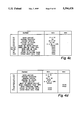
- FIG. 6 illustrates the microprocessor memory map in the microprocessor mode
- FIG. 7a-d illustrate the bit assignation of the control status and data ports in the microprocessor mode
- FIG. 8a-f illustrate the timing diagrams for the microprocessor mode
- the multifunctional ASIC device to be described is designed to perform three standard spacecraft functions, selected by setting the configuration of its pins.
- the device has 68 pins, and the configuration pin input status and pin listing for each mode are given in the appendix.
- the three functions are the thruster drive mode, microprocessor mode and bypass mode and will be described below.
- the ASIC 10 has serial telecommand and telemetry ports 12,14 respectively for receiving ESA AS32/CS32 or AS16/CS16 type telemetry/control signals as previously identified.
- Data arriving at the telecommand port 12 is converted by a serial in parallel out (SIPO) converter 16 and supplied to a register 18.
- Telemetry Data is converted from parallel into serial format by a parallel in serial out (PISO) converter 19 and then supplied to the telemetry port 14.
- SIPO serial in parallel out
- PISO parallel in serial out
- the ASIC device 10 In the thruster drive mode, as shown in more detail in FIG. 2, the ASIC device 10 generates two thruster firing pulses on lines 20 and 22 with the following telecommanded parameters:
- Additional secondary control telecommanded parameters are:
- the telecommand/telemetry standard in this mode is similar to the ESA Standard (TTC-B-01), extended to 32 bits and includes a second strobe to enable clusters of functions to be controlled.
- a link settable address enables up to 16 chips to be controlled from the same telecommand channel without additional logic.
- the ASIC device is instructed via a 32 bit telecommand interface to generate a pair of thruster drive pulses related in frequency and phase to a spin reference pulse, and of specified duration.
- Each command consists of two 32 bit transmissions denoted words X and Y.
- each 32 bit word consists of two standard 16 bit CS16 transmissions, the bit allocations being as shown in the Figures. It will be seen that only the first CS16 of each pair contains the chip address and so the signals must always be supplied as pairs. The first CS16 has its most significant bit (MSB) set to '0' whilst the second has its MSB set to '1'.
- MSB most significant bit
- the chip address is 5 bits long and hence, with 2 addresses in each chip, 16 devices can be controlled from the same command channel.
- the two 32 bit telemetry bits also denoted X and Y are generated to enable confirmation of the commanded status and to supply extra housekeeping data.
- the telemetry signals are read as two 32 bit words each consisting of 2 standard 16 bit AS16 transmissions. Since only the first AS16 contains the address the signals are always read as pairs. The first AS16 has its MSB set to '0' while the second sets its MSB to '1'. In order to facilitate the correct reading of telemetry two extra strobes are required which encompass each pair of AS16 words.
- the bit allocations are also given in these Figures.
- FIG. 4a-d The timing diagrams for the thruster drive mode for both telecommand (Memory Load Command) and Serial Telemetry are shown in FIG. 4a-d.
- the thruster sequence can be enabled (or disabled) by the manoeuvre enable (disable) signals following the next spin reference pulse. Either or both thruster pulses can be enabled by the X -- 2 command word.
- An elapsed timer is maintained, initialised by word Y -- 2 command, decremented by the 1Hz clock when in continuous mode or by the generated thruster pulses when in pulsed mode. This timer is readable in the Y telemetry. Space command and housekeeping telemetry bits are brought out to pins on the device.
- the signal at the parameter latch 30 is then used to instruct a frequency counter 36, a phase counter 38 and a duration counter 40 which in turn supply control signals to the thruster select logic 42 which controls operation of two thrusters 'A' and 'B' by control lines 20 and 22 respectively.
- the thruster select logic is enabled by an execute logic circuit 44 dependent on manoeuvre enable and manoeuvre disable signals respectively.
- signals from the parameter, housekeeping and elapsed time counter latches 30, 32 and 34 are supplied to a multiplexer 46 thence to a 32 bit PISO converter 19. The serial telemetry data is then output for transmission.
- the configuration pin input status is adjusted and the pins have the microprocessor mode input and output functions as shown in the pin listing in the appendix.
- FIG. 5 shows operation in the microprocessor mode.
- the ASIC device provides all the signals necessary to interface between a MIL-STD-1750A microprocessor and a duplex serial interface consisting of one AS16 telemetry and one CS16 telecommand channel as defined in ESA Document TTC-B-01 Issue 1.
- the telecommand complete flag and, if enabled, the telecommand interrupt line will be set.
- the software would then respond by reading the data from the data port. This reading by the software will then reset the telecommand complete flag and will clear the interrupt.
- the telemetry complete flag and, if enabled, the telemetry interrupt line will be set.
- the software would then respond by writing new data to the data port. This writing by the software will then reset the telemetry complete flag and will clear the interrupt. Since no software action will occur until the flag or interrupt is set then it may be necessary also to set a default telemetry word in the data register during initialisation. If not set then this data will be 0000 hex. on power up.
- Telemetry data can be repetitively read without corruption from the serial port, as can telecommand data be repetitively read without corruption by the processor.
- telecommand data can be overwritten at any time by the serial telecommand channel and telemetry data can be overwritten at any time by the processor. If the processor writes to the telemetry whilst it is transmitting, then this data will be latched for the next telemetry request and will not affect the current transmission.
- the microprocessor memory map is shown in FIG. 6.
- the control/status and data addresses of the chip are set jointly by the chip select input being asserted low, and Address bit 15 (LSB) input as the address part of the multiplexed Address/Data bit 15 (AD15). It will be noted that the decode of address bits 0-14 are external to the chip.
- FIGS. 7a-d The bit assignation of the control, status and data ports are shown in FIGS. 7a-d and the timing diagrams are shown in FIGS. 8a-f.
- memory load command data is clocked into a 32 bit SIPO 16 which functions as a 16 bit SIPO.
- Data is then presented at a 16 bit latch 48 where it passes via a 16 bit buffer 50 to the microprocessor interface 52.
- data passes from the interface 52 to a 16 bit latch 54 then via a buffer 56 to the PISO converter 18 and then transmitted via the telemetry port.
- Serial telecommand data passes via a SIPO converter 16 to a register 18 for being presented either to the register output or back to a PISO converter 18 for return as telemetry data.
- FIGS. 10 and 11 are simplified block diagrams showing the ASIC 10 in Thruster Drive Mode and Bypass Mode respectively to illustrate the commonality of the circuitry shared between the three different modes.
- the commonality of function is also apparent from the dotted lines in FIG. 5 which show where the circuit elements specific to the thruster drive mode interface with the PISO converter 19, SIPO converter 16 and the register/latch 14/48, and again from a study of the pin listings in the appendix to see where the pins are used for the same or analogous functions.
Abstract
A multifunctional application specific integrated circuit (ASIC) may be configured to perform one of three different functions by selecting the input status of particular pins on the ASIC. The pins serve various functions according to the set operational mode of the ASIC. The three modes described are a thruster drive mode, a microprocessor interface drive and a bypass mode.
Description
This invention relates to data processing apparatus for use on board a spacecraft and in particular, but not exclusively, to such apparatus implemented in Application Specific Integrated Circuits (ASICs).
Many of the functions on board a spacecraft are controlled remotely and require the exchange of control signals between the spacecraft and a remote control station. For example the jet thrusters on board the spacecraft used for station-keeping are typically contrcilled in accordance with telecommanded signals generated at the remote control station and, as part of the control loop, the spacecraft returns telemetry signals to the remote station. Spinning spacecraft often have multiple thrusters thus requiring several control circuits and these can be extravagant in terms both of payload weight and power consumption.
Accordingly, in one aspect of this invention we have designed an ASIC functioning as a spacecraft thruster drive controller. This provides significant reductions in payload and power consumption, and of the order of 25 % in some cases.
Telecommand data to the spacecraft and telemetry data returned to the remote control station usually follow a serial data standard, a typical example being that set out in the European Space Agency (ESA) document TTC-B-01 Issue 1, which defines one AS16 telemetry channel and one CS16 command channel. The standard can readily be extended to 32 bits.
Given that there is a common serial data standard adopted for communication to and from the spacecraft, we have found that a circuit--typically an ASIC--designed to operate, say, as a thruster drive controller, can be made to operate as an interface allowing duplex transmission of serial data to and from a microprocessor or databus on board the spacecraft with only minor modification of the circuit. In other words, the thruster controller and the interface referred to above handle data in similar formats in use and have several if not most circuit elements in common. Thus, the high costs of developing an ASIC, say, to provide thrust drive control, can be significantly offset if the ASIC is modified to include some sort of function selection and, if necessary, further circuit elements appropriate to the further functions envisaged. The ability to provide such multi-function capability is dependent largely on the selection of the appropriate circuit elements for a particular function which preferably may be readily adapted to provide alternative functions.
Accordingly, in another aspect this invention provides an application specific integrated circuit (ASIC) for use on board a spin-stabilised spacecraft to function as a duplex serial interface to control and monitor the thrusters on the spacecraft, said application specific integrated circuit including serial-to-parallel converter means for converting serial telecommand data into parallel format, means for storing said converted telecommand data for subsequent control of thruster timing pulses, means for receiving and storing telemetry data from said thrusters, and parallel-to-serial converter means for converting said stored telemetry data into serial format for transmission.
The invention may be performed in various ways and, by way of example only, an embodiment thereof, comprising a multifunctional ASIC device will now be described in detail, reference being made to the accompanying drawings, in which:
FIG. 1 is a schematic view illustrating the circuit elements of the multifunctional ASIC device which are shared between its three functions;
FIG. 2 is a block diagram representing the multifunctional ASIC device when operating in the thruster drive mode;
FIGS. 3a-b illustrate the bit allocations of the command and telemetry words in the thruster drive mode;
FIG. 4a-d illustrate the timing diagrams for the thruster device mode;
FIG. 5 is a block diagram representing the multifunctional ASIC device when operating in the microprocessor mode,
FIG. 6 illustrates the microprocessor memory map in the microprocessor mode;
FIG. 7a-d illustrate the bit assignation of the control status and data ports in the microprocessor mode;
FIG. 8a-f illustrate the timing diagrams for the microprocessor mode,
FIG. 9 is a simplified block diagram representing the multifunctional ASIC device when operating in the bypass mode, and
FIGS. 10 and 11 are simplified block diagrams of the ASIC while operating in the Thruster Drive Mode and the microprocessor mode, for comparison with FIG. 9.
The multifunctional ASIC device to be described is designed to perform three standard spacecraft functions, selected by setting the configuration of its pins. The device has 68 pins, and the configuration pin input status and pin listing for each mode are given in the appendix. The three functions are the thruster drive mode, microprocessor mode and bypass mode and will be described below.
Referring to FIG. 1, the ASIC 10 has serial telecommand and telemetry ports 12,14 respectively for receiving ESA AS32/CS32 or AS16/CS16 type telemetry/control signals as previously identified. Data arriving at the telecommand port 12 is converted by a serial in parallel out (SIPO) converter 16 and supplied to a register 18. Telemetry Data is converted from parallel into serial format by a parallel in serial out (PISO) converter 19 and then supplied to the telemetry port 14.
In the thruster drive mode, as shown in more detail in FIG. 2, the ASIC device 10 generates two thruster firing pulses on lines 20 and 22 with the following telecommanded parameters:
division repetition rate with reference to the spin reference pulses (i.e. frequency).
phase delay relative to individual spin reference pulses, and
duration of thruster pulses.
Additional secondary control telecommanded parameters are:
elapsed time set
chip address
individual pulse enables (A and B)
mode selections
When used on spinning satellites with multiple thrusters, considerable savings on hardware can be achieved. The telecommand/telemetry standard in this mode is similar to the ESA Standard (TTC-B-01), extended to 32 bits and includes a second strobe to enable clusters of functions to be controlled. A link settable address enables up to 16 chips to be controlled from the same telecommand channel without additional logic. In the thruster drive mode the ASIC device is instructed via a 32 bit telecommand interface to generate a pair of thruster drive pulses related in frequency and phase to a spin reference pulse, and of specified duration. Each command consists of two 32 bit transmissions denoted words X and Y.
Referring to FIGS. 3a-h, each 32 bit word consists of two standard 16 bit CS16 transmissions, the bit allocations being as shown in the Figures. It will be seen that only the first CS16 of each pair contains the chip address and so the signals must always be supplied as pairs. The first CS16 has its most significant bit (MSB) set to '0' whilst the second has its MSB set to '1'. The chip address is 5 bits long and hence, with 2 addresses in each chip, 16 devices can be controlled from the same command channel.
The two 32 bit telemetry bits also denoted X and Y are generated to enable confirmation of the commanded status and to supply extra housekeeping data. The telemetry signals are read as two 32 bit words each consisting of 2 standard 16 bit AS16 transmissions. Since only the first AS16 contains the address the signals are always read as pairs. The first AS16 has its MSB set to '0' while the second sets its MSB to '1'. In order to facilitate the correct reading of telemetry two extra strobes are required which encompass each pair of AS16 words. The bit allocations are also given in these Figures.
The timing diagrams for the thruster drive mode for both telecommand (Memory Load Command) and Serial Telemetry are shown in FIG. 4a-d.
When both words X and Y have been correctly loaded, confirmable by telemetry, then the thruster sequence can be enabled (or disabled) by the manoeuvre enable (disable) signals following the next spin reference pulse. Either or both thruster pulses can be enabled by the X -- 2 command word.
An elapsed timer is maintained, initialised by word Y -- 2 command, decremented by the 1Hz clock when in continuous mode or by the generated thruster pulses when in pulsed mode. This timer is readable in the Y telemetry. Space command and housekeeping telemetry bits are brought out to pins on the device.
In the thruster drive mode, memory load command data is supplied in serial format to the 32 bit SIPO converter 16 on line 21 in accordance with strobe and clock signals on lines 23 and 24 respectively, as seen in the timing diagram in FIG. 4a. The 5-bit address code is checked by an address decoder 26 which supplies a signal to the telecommand control logic 28. Following conversion at the SIPO Converter 16, the X -- 1 and X -- 2 words are passed to a 32 bit parameter latch 30 and the Y -- 1 and Y -- 2 words are passed to a 16 bit housekeeping latch 32 and a 16 bit Elapsed Time Counter latch 34 respectively. The signal at the parameter latch 30 is then used to instruct a frequency counter 36, a phase counter 38 and a duration counter 40 which in turn supply control signals to the thruster select logic 42 which controls operation of two thrusters 'A' and 'B' by control lines 20 and 22 respectively. The thruster select logic is enabled by an execute logic circuit 44 dependent on manoeuvre enable and manoeuvre disable signals respectively. At the telemetry side, signals from the parameter, housekeeping and elapsed time counter latches 30, 32 and 34 are supplied to a multiplexer 46 thence to a 32 bit PISO converter 19. The serial telemetry data is then output for transmission.
For the microprocessor mode, the configuration pin input status is adjusted and the pins have the microprocessor mode input and output functions as shown in the pin listing in the appendix.
FIG. 5 shows operation in the microprocessor mode. In the microprocessor mode, the ASIC device provides all the signals necessary to interface between a MIL-STD-1750A microprocessor and a duplex serial interface consisting of one AS16 telemetry and one CS16 telecommand channel as defined in ESA Document TTC-B-01 Issue 1.
Normally, during software initialisation, the microprocessor would clear any residual Interrupts and the TM/TC complete status and enable interrupts. This would be accomplished using the control port (if using a polling method then the interrupts would not be enabled).
Whenever a serial command is received, then at the end of the STROBE the telecommand complete flag and, if enabled, the telecommand interrupt line will be set. The software would then respond by reading the data from the data port. This reading by the software will then reset the telecommand complete flag and will clear the interrupt.
Similarly, whenever serial telemetry is requested, then at the end of the SAMPLE the telemetry complete flag and, if enabled, the telemetry interrupt line will be set. The software would then respond by writing new data to the data port. This writing by the software will then reset the telemetry complete flag and will clear the interrupt. Since no software action will occur until the flag or interrupt is set then it may be necessary also to set a default telemetry word in the data register during initialisation. If not set then this data will be 0000 hex. on power up.
Telemetry data can be repetitively read without corruption from the serial port, as can telecommand data be repetitively read without corruption by the processor. In addition, telecommand data can be overwritten at any time by the serial telecommand channel and telemetry data can be overwritten at any time by the processor. If the processor writes to the telemetry whilst it is transmitting, then this data will be latched for the next telemetry request and will not affect the current transmission.
The microprocessor memory map is shown in FIG. 6. The control/status and data addresses of the chip are set jointly by the chip select input being asserted low, and Address bit 15 (LSB) input as the address part of the multiplexed Address/Data bit 15 (AD15). It will be noted that the decode of address bits 0-14 are external to the chip.
The bit assignation of the control, status and data ports are shown in FIGS. 7a-d and the timing diagrams are shown in FIGS. 8a-f.
Returning to FIG. 5, in the microprocessor mode, memory load command data is clocked into a 32 bit SIPO 16 which functions as a 16 bit SIPO. Data is then presented at a 16 bit latch 48 where it passes via a 16 bit buffer 50 to the microprocessor interface 52. In the other direction, data passes from the interface 52 to a 16 bit latch 54 then via a buffer 56 to the PISO converter 18 and then transmitted via the telemetry port.
In the bypass mode, the configuration pin input status is adjusted and the pins have the input and output functions as shown in the appendix. Referring to FIG. 9, in the bypass mode, the chip provides a simple reflected serial command and telemetry hardware channel with a latched 16 bit register output. The chip provides an interface to a 16 bit latch from a serial CS16 telecommand channel. The latch is readable from a serial AS16 telemetry channel. All timing of the telecommand/telemetry data channel is identical to the microprocessor mode. The latch is initially set to all zeroes on power up and is then updated at the end of each signal data strobe, remaining unchanged at all other times including during serial data transmission.
Serial telecommand data passes via a SIPO converter 16 to a register 18 for being presented either to the register output or back to a PISO converter 18 for return as telemetry data.
FIGS. 10 and 11 are simplified block diagrams showing the ASIC 10 in Thruster Drive Mode and Bypass Mode respectively to illustrate the commonality of the circuitry shared between the three different modes. The commonality of function is also apparent from the dotted lines in FIG. 5 which show where the circuit elements specific to the thruster drive mode interface with the PISO converter 19, SIPO converter 16 and the register/latch 14/48, and again from a study of the pin listings in the appendix to see where the pins are used for the same or analogous functions.
It will be appreciated from the appendix that the pins of the ASIC 10 serve different functions according to the operating mode of the ASIC, thus reducing the number of pins required on the ASIC.
__________________________________________________________________________ APPENDIX 1/3 Configuration Table This table defines the configuration pin input status required to set the different functional modes. Pins Pins 42, 50, 51, Pin Pin Pin 57, 53, Pin Pin Pin Pin Pin 61 62 66 58, 67 39 40 47 63 49 __________________________________________________________________________Thruster Drive Mode 0 0 x x x x x x 0 xMicroprocessor Mode 0 1 0 1 0 x x x 0x Bypass Mode 0 1 1 1 0 0 1 0 0 0Test Mode 1 x x x x x x x x x (note this is reserved for factory testing purposes) __________________________________________________________________________ (note; an x in this table denotes a used dynamic input, not a don't care condition. Its function is detailed in the more comprehensive pin listing below.)
  Pin Listing Pin Thruster Drive Mode Microprocessor Mode Bypass Mode No. M
 nemonic Description IO Mnemonic Description IO Mnemonic Description
 IO     APPENDIX 2/3  1 Vss Ground I Vss Ground I Vss Ground I  2
 APBX.sub.-- 4 Block X Address patch I INTR.sub.-- 2 Interrupt 2,
 (Telecommand) O NU not used O       3 APBX.sub.-- 5 Block X Address
 patch I AD.sub.-- 0 Address Data Bus 0 (MSB) IO D0 Data bit 0 (MSB) O
 (LSB)  4 APBY.sub.-- 1 Block Y Address patch I AD.sub.-- 1 Address Data
 Bus 1 IO D1 Data bit 1 O   (MSB)  5 APBY.sub.-- 2 Block Y Address patch
 I AD.sub.-- 2 Address Data Bus 2 IO D2 Data bit 2 O  6 APBY.sub.-- 3
 Block Y Address patch I AD.sub.-- 3 Address Data Bus 3 IO D3 Data bit 3
 O  7 APBY.sub.-- 4 Block Y Address patch I AD.sub.-- 4 Address Data Bus
 4 IO D4 Data bit 4 O  8 APBY.sub.-- 5 Block Y Address patch I AD.sub.--
 5 Address Data Bus 5 IO D5 Data bit 5 O   (LSB)  9 Vdd +5v I Vdd +5v I
 Vdd +5v I 10 L.sub.-- 6.sub.-- OUT Block Y Telecommand O NU not used O
 NU not used O   discrete output 11 HK.sub.-- 6.sub.-- IN Block Y
 Housekeeping I AD.sub.-- 6 Address Data Bus 6 IO D6 Data bit 6 O
 Telemetry input 12 L.sub.-- 7.sub.-- OUT Block Y Telecommand O NU not
 used O NU not used O   discrete output 13 HK.sub.-- 7.sub.-- IN Block Y
 Housekeeping I AD.sub.-- 7 Address Data Bus 7 IO D7 Data bit 7 O
 Telemetry input 14 L.sub.-- 8.sub.-- OUT Block Y Telecommand O NU not
 used O NU not used O   discrete output 15 HK.sub.-- 8.sub.-- IN Block Y
 Housekeeping I AD.sub.-- 8 Address Data Bus 8 IO D8 Data bit 8 O
 Telemetry input 16 L.sub.-- 9.sub.-- OUT Block Y Telecommand O NU not
 used O NU not used O   discrete output 17 HK.sub.-- 9.sub.-- IN Block Y
 Housekeeping I AD.sub.-- 9 Address Data Bus 9 IO D9 Data bit 9 O
 Telemetry input 18 Vss Ground I Vss Ground I Vss Ground I 19 L.sub.--
 10.sub.-- OUT Block Y Telecommand O NU not used O NU not used O
 discrete output 20 HK.sub.-- 10.sub.-- IN Block Y Housekeeping I
 AD.sub.-- 10 Address Data Bus 10 IO D10 Data bit 10 O   Telemetry input
 21 L.sub.-- 11.sub.-- OUT Block Y Telecommand O NU not used O NU not
 used O   discrete output 22 HK.sub.-- 11.sub.-- IN Block Y Housekeeping
 I AD.sub.-- 11 Address Data Bus 11 IO D11 Data bit 11 O   Telemetry
 input 23 L.sub.-- 12.sub.-- OUT Block Y Telecommand O NU not used O NU
 not used O   discrete output 24 HK.sub.-- 12.sub.--
  IN Block Y Housekeeping I AD.sub.-- 12 Address Data Bus 12 IO D12 Data
 bit 12 O   Telemetry input 25 L.sub.-- 13.sub.-- OUT Block Y Telecommand
 O NU not used O NU not used O   discrete output 26 HK.sub.-- 13.sub.--
 IN Block Y Housekeeping I AD.sub.-- 13 Address Data Bus 13 IO D13 Data
 bit 13 O   Telemetry input 27 L.sub.-- 14.sub.-- OUT Block Y Telecommand
 O NU not used O NU not used O   discrete output 28 HK.sub.-- 14.sub.--
 IN Block Y Housekeeping I AD.sub.-- 14 Address Data Bus 14 IO D14 Data
 bit 14 O   Telemetry input 29 L.sub.-- 15.sub.-- OUT Block Y Telecommand
 O NU not used O NU not used O   discrete output 30 HK.sub.-- 15.sub.--
 IN Block Y Housekeeping I AD.sub.-- 15 Address Data Bus 15 (LBS) IO
 D.sub.-- 15D15 Data bit 15 (LSB) O   Telemetry input 31 Vdd +5v I Vdd
 +5v I Vdd +5v I 32 TM.sub.-- DATA.sub.-- Y.sub.-- OUT.sub.-- A Block Y
 Telemetry data TS NU not used O NU not used O   serial data output O 33
 TM.sub.-- DATA.sub.-- Y.sub.-- OUT Block Y Telemetry data TS NU not used
 O NU not used O   serial data output (copy) O 34 TM.sub.-- DATA.sub.--
 X.sub.-- OUT Block X Telemetry data TS TM.sub.-- DATA AS16 Telemetry
 data output TS TM.sub.-- DATA AS16 Telemetry data output TS   serial
 data output O .sub.-- OUT  O .sub.-- OUT  O APPENDIX 3/3 35 TM.sub.--
 DATA.sub.-- X.sub.-- OUT.sub.-- A Block X Telemtery data TS TM.sub.--
 DATA AS16 Telemetry data output TS TM.sub.-- DATA AS16 Telemetry data
 output (copy) TS   serial data output (copy) O .sub.-- OUT.sub.-- A
 (copy) O .sub.-- OUT.sub.-- A  O 36 Vss Ground I Vss Ground I Vss Ground
 I 37 M.sub.-- 29.sub.-- OUT Block X TC, Bit 29 O M.sub.-- 29.sub.-- OUT
 not used output O M.sub.-- 29.sub.-- OUT connect to M.sub.-- 29.sub.--
 IN O 38 M.sub.-- 29.sub.-- IN Block X TM, Bit 29 I/P I M.sub.--
  29.sub.-- IN input, connect to 0 I M.sub.-- 29.sub.-- IN connect to
 M.sub.-- 29.sub.-- OUT I 39 TM.sub.-- STROBE.sub.-- Y Block Y Telemetry
 Strobe I DSB Data Strobe I NU set to 0v I   40 TM.sub.-- SAMPLE.sub.--
 YB Block Y Telemetry Sample I RD.sub.-- WRB Read/Write I NU set to +5v I
   41 TM.sub.-- SAMPLE.sub.-- XB Block X Telemetry Sample I TM Telemetry
 Sample I TM Telemetry Sample I     .sub.-- SAMPLEB   .sub.-- SAMPLEB 42
 TM.sub.-- STROBE.sub.-- X Block X Telemetry Strobe I NU connect to 0v I
 NU set to 0v I   43 TM.sub.-- CKB Telemetry Clock I TM.sub.-- CKB
 Telemetry Clock I TM.sub.-- CKB Telemetry Clock I 44 ML.sub.-- CKB
 Memory Load Clock I ML.sub.-- CKB Memory Load Clock I ML.sub.-- CKB
 Memory Load Clock I 45 ML.sub.-- STROBEB Memory Load Strobe I ML.sub.--
 STROBEB Memory Load Strobe I ML.sub.-- STROBEB Memory Load Strobe I 46
 ML.sub.-- DATA Memory Load Data I ML.sub.-- DATA Memory Load Data I
 ML.sub.-- DATA Memory Load Data I 47 SSC Spin Segement Clock I SELECTB
 Address Chip Select I NU set to +0v I 48 SRP Spin Reference Pulse I RDYB
 Ready O NU not used O 49 CLOCK.sub.-- 131K 131 kHz clock I AS Address
 Strobe I NU set to 0v I 50 CLOCK.sub.-- 1HZ 1 Hz clock I NU set to +5v I
 NU set to +5v I 51 EXECUTE Enable execution of thruster I NU set to 0v I
 NU set to 0v I   drive function following next   sun reference pulse 52
 Vdd +5v  Vdd +5v I Vdd +5v I 53 MAN.sub.-- ACT.sub.-- IN Block Y
 Housekeeping I NU set to 0v I NU set to 0v I   Telemetry input (Manoeuvre
    active) 54 MAN.sub.-- ACT.sub.-- OUT Manoeuvre active output (= O NU
 no connection O NU not used O   TC Block X bit 30.bit31 =   selectA and
 SelectB) 55 L.sub.-- 31.sub.--
  OUT Block Y Telecommand O NU no connection O NU not used O   discrete
 output 56 LOAD.sub.-- DET.sub.-- OUTB Telecommand Detected O NU no
 connection O NU not used O   correct address 57 DISABLE.sub.-- 2B
 Disable Thruster Drive I NU set to 5v I NU set to +5v I   function 58
 DISABLE.sub.-- 1B Disable Thruster Drive I NU set to +5v I NU set to +
 5v I   function (either A or B will   disable it) 59 PO.sub.-- RESETB
 Power On Reset I PO.sub.-- RESETB Power On Reset I PO.sub.-- RESETB
 Power On Reset I 60 TD.sub.-- OUT Test Data Out, not used O TD.sub.--
 OUT Test Data Out, not used O TD.sub.-- OUT Test Data out, not used O 61
 TM.sub.-- SEL Test Mode Select, set to 0v I TM.sub.-- SEL Test Mode
 Select, set to 0v I TM.sub.-- SEL Test Mode Select, set to 0v I 62
 TD.sub.-- MODEB Test Data In, I UP.sub.-- MODE Test Data In, I UP MODE
 Test Data In, I  (TD.sub.-- IN) TD configuration,  (TD.sub.-- IN) uP
 configuration,  (TD.sub.-- IN) Bypass mode,   set to 0v   set to +5v
 set to +5v 63 NU Test Clock, I NU set to 0v I NU Not used, I  (T.sub.--
 CK.sub.-- IN) not used,  (T.sub.-- CK.sub.-- IN)    SET TO 0v   set to
 0v  64 DRIVE.sub.-- B Thruster Drive B O NU Not used O NU Not used O 65
 DRIVE.sub.-- A Thruster Drive A O NU Not used O NU Not used O 66
 APBX.sub.-- 1 Block X Address patch I BYPASS Enables Microprocessor I
 BYPASS Enables Bypass mode, I   (MSB)   function if "0",   set to +5v
   set to 0v 67 APBX.sub.-- 2 Block X Address patch I NU Not used, I NU
 Not used, I      set to 0v   set to 0v 68 APBX.sub.-- 3 Block X Address
 patch I INTR.sub.--
  1 Interrupt 1, O NU Not used O      (Telemetry)
Claims (4)
1. A multi-function application specific integrated circuit for a spin-stabilized spacecraft whose position and/or orientation is controlled in use by thruster means on board the spacecraft, said integrated circuit being operable for passing serial data between said spacecraft and a remote command station, said integrated circuit including:
command data input means for receiving from said command station serial command data encoding thruster control signals;
serial to parallel converter means for receiving from said data input means said serial data and converting it to parallel format;
command store means for storing parallel data output by said serial to parallel converter means;
thruster control means for receiving from said command store means parallel data and for extracting therefrom thruster control signals;
telemetry data input means for receiving parallel telemetry data;
telemetry store means for storing said parallel telemetry data;
parallel to serial converter means for receiving parallel telemetry data from said telemetry store means and converting it into serial format;
telemetry data output means for receiving serial data from said parallel to serial converter means and passing it for output to said remote station;
mode selecting means for selecting the operating mode of said integrated circuit; and
microprocessor parallel interface means for receiving data from said command store means, and transmitting data to said telemetry store means, wherein in a microprocessor mode data supplied to said command data input means is passed to said microprocessor interface means and data from said interface means is passed to said telemetry data output means.
2. A multi-function application specific integrated circuit according to claim 1, including bypass means operable to pass data stored in said command store means to said telemetry data input means, wherein the integrated circuit provides a reflected serial command and telemetry channel, and means for setting said mode selecting means to select a bypass mode in which said bypass means is rendered operable.
3. A multi-function application specific integrated circuit according to claim 1, including a plurality of input and output terminal means for passing data to or from said command data input means and said telemetry data output means, wherein said mode selection means is responsive to application of predetermined signals to selected ones of said terminal means.
4. A control assembly for a spin stabilized spacecraft whose position and/or orientation is controlled in use by thruster means on board the spacecraft, said control assembly being operable for passing serial data between said spacecraft and a remote command station, said control assembly comprising a plurality of integrated circuits, each integrated circuit including:
command data input means for receiving from said command station serial command data encoding thruster control signals;
serial to parallel converter means for receiving from said data input means said serial data and converting it to parallel format;
command store means for storing parallel data output by said serial to parallel converter means;
thruster control means for receiving from said store means parallel data and for extracting therefrom thruster control signals;
telemetry data input means for receiving parallel telemetry data;
telemetry store means for storing said parallel telemetry data;
parallel to serial converter means for receiving parallel data from said telemetry store means and converting it into serial format;
telemetry data output means for receiving serial data from said parallel to serial converter means and passing it for output to said remote station;
mode selecting means for selecting the operating mode of said integrated circuit; and
microprocessor parallel interface means for receiving data from said command store means and transmitting data to said telemetry store means wherein in a microprocessor mode data supplied to said command data input means is passed to said microprocessor interface means and data from said interface means is passed to said telemetry data output means.
Applications Claiming Priority (2)
| Application Number | Priority Date | Filing Date | Title |
|---|---|---|---|
| GB9117187 | 1991-08-08 | ||
| GB9117187A GB2259377B (en) | 1991-08-08 | 1991-08-08 | Multi-function application specific integrated circuit for controlling spacecraft thrusters |
Publications (1)
| Publication Number | Publication Date |
|---|---|
| US5396428A true US5396428A (en) | 1995-03-07 |
Family
ID=10699732
Family Applications (1)
| Application Number | Title | Priority Date | Filing Date |
|---|---|---|---|
| US07/925,276 Expired - Fee Related US5396428A (en) | 1991-08-08 | 1992-08-06 | Multi-function application specific integrated circuit for controlling spacecraft thrusters |
Country Status (3)
| Country | Link |
|---|---|
| US (1) | US5396428A (en) |
| EP (1) | EP0530975A3 (en) |
| GB (1) | GB2259377B (en) |
Cited By (7)
| Publication number | Priority date | Publication date | Assignee | Title |
|---|---|---|---|---|
| US5793656A (en) * | 1994-06-30 | 1998-08-11 | Hughes Electronics Corporation | Application-specific integrated circuits having programming functions |
| US6047361A (en) * | 1996-08-21 | 2000-04-04 | International Business Machines Corporation | Memory control device, with a common synchronous interface coupled thereto, for accessing asynchronous memory devices and different synchronous devices |
| US6496741B1 (en) | 1999-03-25 | 2002-12-17 | Gregory J. Whiffen | Static/dynamic control for optimizing a useful objective |
| CN1303747C (en) * | 2002-05-06 | 2007-03-07 | O2米克罗公司 | Converter controller |
| US20080187051A1 (en) * | 2007-02-01 | 2008-08-07 | Takuma Chiba | Image coding apparatus and image decoding apparatus |
| CN1781333B (en) * | 2003-06-10 | 2011-03-30 | 思科技术公司 | System packet interface |
| US8760328B1 (en) | 2012-09-14 | 2014-06-24 | Altera Corporation | Interface circuitry for an integrated circuit system |
Citations (6)
| Publication number | Priority date | Publication date | Assignee | Title |
|---|---|---|---|---|
| US3763472A (en) * | 1972-03-27 | 1973-10-02 | Burroughs Corp | Distributing and collecting memory array and transfer system |
| US3975712A (en) * | 1975-02-18 | 1976-08-17 | Motorola, Inc. | Asynchronous communication interface adaptor |
| GB2097564A (en) * | 1981-03-07 | 1982-11-03 | British Aerospace | Spacecraft control system |
| US4426685A (en) * | 1978-03-20 | 1984-01-17 | The United States Of America As Represented By The Secretary Of The Navy | Solid state delay device |
| US4855735A (en) * | 1986-12-06 | 1989-08-08 | Rolls-Royce Plc | Recovery of data clock signals |
| US5070338A (en) * | 1989-08-24 | 1991-12-03 | General Electric Company | Doppler determination of satellite attitude |
-
1991
- 1991-08-08 GB GB9117187A patent/GB2259377B/en not_active Expired - Fee Related
-
1992
- 1992-08-03 EP EP19920307076 patent/EP0530975A3/en not_active Withdrawn
- 1992-08-06 US US07/925,276 patent/US5396428A/en not_active Expired - Fee Related
Patent Citations (7)
| Publication number | Priority date | Publication date | Assignee | Title |
|---|---|---|---|---|
| US3763472A (en) * | 1972-03-27 | 1973-10-02 | Burroughs Corp | Distributing and collecting memory array and transfer system |
| US3975712A (en) * | 1975-02-18 | 1976-08-17 | Motorola, Inc. | Asynchronous communication interface adaptor |
| GB1507761A (en) * | 1975-02-18 | 1978-04-19 | Motorola Inc | Asynchronous communication interface adaptor |
| US4426685A (en) * | 1978-03-20 | 1984-01-17 | The United States Of America As Represented By The Secretary Of The Navy | Solid state delay device |
| GB2097564A (en) * | 1981-03-07 | 1982-11-03 | British Aerospace | Spacecraft control system |
| US4855735A (en) * | 1986-12-06 | 1989-08-08 | Rolls-Royce Plc | Recovery of data clock signals |
| US5070338A (en) * | 1989-08-24 | 1991-12-03 | General Electric Company | Doppler determination of satellite attitude |
Cited By (8)
| Publication number | Priority date | Publication date | Assignee | Title |
|---|---|---|---|---|
| US5793656A (en) * | 1994-06-30 | 1998-08-11 | Hughes Electronics Corporation | Application-specific integrated circuits having programming functions |
| US6047361A (en) * | 1996-08-21 | 2000-04-04 | International Business Machines Corporation | Memory control device, with a common synchronous interface coupled thereto, for accessing asynchronous memory devices and different synchronous devices |
| US6496741B1 (en) | 1999-03-25 | 2002-12-17 | Gregory J. Whiffen | Static/dynamic control for optimizing a useful objective |
| CN1303747C (en) * | 2002-05-06 | 2007-03-07 | O2米克罗公司 | Converter controller |
| CN1781333B (en) * | 2003-06-10 | 2011-03-30 | 思科技术公司 | System packet interface |
| US20080187051A1 (en) * | 2007-02-01 | 2008-08-07 | Takuma Chiba | Image coding apparatus and image decoding apparatus |
| US8102919B2 (en) * | 2007-02-01 | 2012-01-24 | Panasonic Corporation | Image coding apparatus and image decoding apparatus |
| US8760328B1 (en) | 2012-09-14 | 2014-06-24 | Altera Corporation | Interface circuitry for an integrated circuit system |
Also Published As
| Publication number | Publication date |
|---|---|
| GB9117187D0 (en) | 1991-10-09 |
| EP0530975A3 (en) | 1994-05-11 |
| GB2259377B (en) | 1995-06-21 |
| EP0530975A2 (en) | 1993-03-10 |
| GB2259377A (en) | 1993-03-10 |
Similar Documents
| Publication | Publication Date | Title |
|---|---|---|
| US4138732A (en) | Data transfer control system | |
| US5093780A (en) | Inter-processor transmission system having data link which automatically and periodically reads and writes the transfer data | |
| US4716525A (en) | Peripheral controller for coupling data buses having different protocol and transfer rates | |
| US5014187A (en) | Adapting device for accommodating different memory and bus formats | |
| US7459892B2 (en) | System and method for controlling a point-of-load regulator | |
| US5778195A (en) | PC card | |
| US4309755A (en) | Computer input/output arrangement for enabling a simultaneous read/write data transfer | |
| US4845611A (en) | Device for connecting 8-bit and 16-bit modules to a 16-bit microprocessor system | |
| US4591973A (en) | Input/output system and method for digital computers | |
| US4065810A (en) | Data transfer system | |
| EP0518488A1 (en) | Bus interface and processing system | |
| EP0163305A2 (en) | Cmos type input-output circuit | |
| US5367641A (en) | MIL-STD-1553 interface device having a bus controller minor frame timer | |
| US5325359A (en) | MIL-STD-1553 interface device having concurrent remote terminal and monitor terminal operation | |
| US5345564A (en) | Serial communication peripheral integrated electronic circuit that recognizes its unique address before the entire circuit is enabled | |
| US5396428A (en) | Multi-function application specific integrated circuit for controlling spacecraft thrusters | |
| US4779093A (en) | Bus interface with programmable window for data transfer | |
| EP0464848B1 (en) | Structure for enabling direct memory-to-memory transfer | |
| US5490254A (en) | MIL-STD-1553 interface device having autonomous operation in all modes | |
| EP0482589A2 (en) | Method and apparatus for controlling bus in computer system to which expansion unit is connectable | |
| EP0358424A2 (en) | Data transfer method | |
| DK170081B1 (en) | Data transfer circuit | |
| US5428801A (en) | Data array conversion control system for controlling conversion of data arrays being transferred between two processing systems | |
| EP0169909A1 (en) | Auxiliary memory device | |
| USH1507H (en) | Demand assigned multiple access (DAMA) device controller interface |
Legal Events
| Date | Code | Title | Description |
|---|---|---|---|
| AS | Assignment |
Owner name: BRITISH AEROSPACE SPACE AND COMMUNICATIONS LIMITED Free format text: ASSIGNMENT OF ASSIGNORS INTEREST.;ASSIGNORS:TICHBORNE, FRANKLIN G.;STEVENS, JOHN S.;REEL/FRAME:006239/0073 Effective date: 19920728 |
|
| REMI | Maintenance fee reminder mailed | ||
| LAPS | Lapse for failure to pay maintenance fees | ||
| FP | Lapsed due to failure to pay maintenance fee |
Effective date: 19990307 |
|
| STCH | Information on status: patent discontinuation |
Free format text: PATENT EXPIRED DUE TO NONPAYMENT OF MAINTENANCE FEES UNDER 37 CFR 1.362 |