US5387847A - Passive power factor ballast circuit for the gas discharge lamps - Google Patents
Passive power factor ballast circuit for the gas discharge lamps Download PDFInfo
- Publication number
- US5387847A US5387847A US08/206,512 US20651294A US5387847A US 5387847 A US5387847 A US 5387847A US 20651294 A US20651294 A US 20651294A US 5387847 A US5387847 A US 5387847A
- Authority
- US
- United States
- Prior art keywords
- terminals
- power supply
- circuit
- pair
- capacitor
- Prior art date
- Legal status (The legal status is an assumption and is not a legal conclusion. Google has not performed a legal analysis and makes no representation as to the accuracy of the status listed.)
- Expired - Fee Related
Links
Images
Classifications
-
- H—ELECTRICITY
- H05—ELECTRIC TECHNIQUES NOT OTHERWISE PROVIDED FOR
- H05B—ELECTRIC HEATING; ELECTRIC LIGHT SOURCES NOT OTHERWISE PROVIDED FOR; CIRCUIT ARRANGEMENTS FOR ELECTRIC LIGHT SOURCES, IN GENERAL
- H05B41/00—Circuit arrangements or apparatus for igniting or operating discharge lamps
- H05B41/14—Circuit arrangements
- H05B41/26—Circuit arrangements in which the lamp is fed by power derived from dc by means of a converter, e.g. by high-voltage dc
- H05B41/28—Circuit arrangements in which the lamp is fed by power derived from dc by means of a converter, e.g. by high-voltage dc using static converters
Definitions
- This invention relates to power supply circuits for gas discharge lamps, and more specifically relates to such a power supply circuit having a power factor in excess of 0.95.
- Electronic ballast circuits for gas discharge lamps are well known. Such circuits should have a power factor in excess of 0.95 for more efficient operation and to meet specifications of various organizations and municipalities.
- a very inexpensive ballast circuit manufactured and sold in the Peoples Republic of China, and identified as "Peking Radio Factory #5" employs a rectifier circuit to increase power factor.
- This circuit uses three diodes in series, having two capacitors each having one terminal connected to respective ones of the opposite end terminals of the string of diodes and their other terminals connected to respective nodes between the center diode and the outer two diodes of the three-diode chain.
- the outer ends of the diode chain are connected to the positive and negative output terminals to the lamp circuit. With this connection, the two capacitors will charge in series and discharge in parallel.
- a resistor is added to the rectifier circuit described above, between two of the diodes of the three-diode chain, specifically at the node between the resistor and the cathode terminal of one of the diodes.
- the resistor having a value of 47 ohms and 1 watt in the preferred embodiment of the invention increased the power factor of the circuit to 0.958.
- Other resistance values can be used which also will increase the circuit power factor.
- the reason for the power factor improvement is that the added resistor changes the shape of the current waveform from a spike to a smoother change, in the step waveform, tending to bring the current wave shape more alignment with the sinusoidal voltage, therefore increasing the power factor.
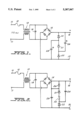
- FIG. 1 is a circuit diagram of a prior art rectifier circuit.
- FIG. 2 is a circuit diagram of the circuit of FIG. 1, but incorporating the improvement of the present invention.
- FIG. 3 is a circuit diagram of a one-half bridge high power factor ballast circuit for a double 40 watt fluorescent lamp circuit.
- FIG. 1 shows a prior art lamp ballast rectifier circuit, identified as a "Peking Radio Factory #5", and was made and sold in the Peoples Republic of China.
- the circuit of FIG. 1 could be used, for example, to drive up to a 100 watt fluorescent lamp with electronic ballast or other load.
- the circuit of FIG. 1 has input a-c terminals 10 and 11 which are connectable to a 115 volt a-c source.
- Terminal 10 is connected to a 2 ampere fuse 12 and then a two-winding transformer 13 and capacitor 14 which act as a noise filter and keep voltage spikes from the ballast circuit from being applied to the a-c line.
- Capacitor 14 is 0.1 microfarad.
- a single phase, full wave bridge rectifier 15 is connected to the terminals of capacitor 14 and its d-c terminals 16 and 17 provide a d-c output to a lamp circuit.
- the bridge 15 consists of four IN4007 diodes.
- a novel circuit consisting of three diodes 20, 21 and 22, poled with their cathodes conducting in the same direction, and two capacitors 23 and 24 connected as shown from lines 16 and 17, respectively, to the nodes between diodes 21-22 and 22-23, respectively.
- Diodes 20, 21 and 22 are each Type IN4007, and capacitors 23 and 24 are each 47 microfarads, 100 volt capacitors.
- Capacitors 23 and 24 charge in series, as the potential at terminal 16 increases, and discharge in parallel when that potential decreases.
- the power factor of the circuit of FIG. 1 has been measured to be 0.935, which is too low for use in numerous applications requiring a power factor greater than 0.95.
- resistor 30 is added between diodes 21 and 22 and one terminal of capacitor 24 is connected to the node between diode 22 and resistor 30.
- resistor 30 is a 1 watt, 47 ohm resistor. Its presence increased the power factor of the circuit to 0.958, and above 0.95.
- Other resistance values could be used, in combination with other values for capacitors 23 and 24, to produce the desired result of a power factor greater than 0.95.
- the resistor 30 acts to reduce the "spiking" of capacitors 23 and 24 during their operation to cause a more gradual current change which more closely matches the input voltage wave shape, thus leading to a higher power factor.
- each of capacitors 23 and 24 charge in series to: V P /2-3V F .
- V P is the peak voltage at terminal and V F is the forward voltage drop of any of the diodes in bridge 15, and diodes 20, 21 and 22.
- capacitors 23 and 24 discharge in parallel to: V P /2-V F .
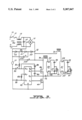
- FIG. 3 shows the application of the novel circuit to a high power factor "Double 40" lamp circuit.
- those components which are the same as the components of FIG. 2 carry the same identifying numerals.
- the circuit of FIG. 3 also contains a half bridge ballast containing a pair of power MOSFETs 40 and 41 which are turned on and off under the control of a MOS gate driver integrated circuit 42 which may be a Type IR2155 and MOSFETs 40 and 41 may be Types IRF624 for a 110 volt a-c input, or IRF730 for a 220 volt input a-c voltage.
- a MOS gate driver integrated circuit 42 which may be a Type IR2155 and MOSFETs 40 and 41 may be Types IRF624 for a 110 volt a-c input, or IRF730 for a 220 volt input a-c voltage.
- the MOSFETs 40 and 41 are connected to drive two 40 watt fluorescent lamps 50 and 51 which have heater windings 52, 53 and 54, 55, respectively.
- a pair of capacitors 56, 57 and 58, 59 are in parallel with tubes 50 and 51, respectively, and thermistors 60 and 61 are in parallel with capacitors 57 and 59, respectively.
- Output terminal 16 is connected through inductors 70 and 71 to heater windings 52 and 54, respectively, while heater windings 53 and 55 are connected, through capacitor 72, to the node between power MOSFETs 40 and 41.
- Output terminal 16 is also connected to the drain electrode of MOSFET 40 and output terminal 17 is connected to the source electrode of MOSFET 41.
- the MOS gate driver 42 is then connected to drive the power MOSFETs 40 and 41 near the natural frequency of oscillation of the circuit including the inductors 70 and 71 and the capacitors associated therewith.
- the H O (high output) pin is connected to the gate of MOSFET 40 and the L O (low output) pin is connected to the gate of MOSFET 41.
- Input power for the chip 42 is derived from terminal 17, through capacitor 80 to pin V CC , and from resistor 81 which is connected to the node between diode 22 and resistor 30.
- Pins R T and C T are connected by resistor 82 and are connected to terminal 17 through capacitor 82.
- the V CC pin is connected to pin V B through diode 84 and to pin V S through capacitor 85.
- control circuit chip 42 will provide turn on signals alternately to power MOSFETs 40 and 41 such that lamps 50 and 51 are connected to the output terminals 16 and 17 when MOSFET 41 is on and MOSFET 40 is off and drive recirculating current through MOSFET 40 when it turns on and MOSFET 41 turns off.
- the tubes 50 and 51 are efficiently driven at a relatively high frequency, for example, 30 to 70 kilohertz, while the circuit exhibits a high power factor, in excess of 0.95 by virtue of the presence of resistor 30.
Abstract
Description
Claims (24)
Priority Applications (1)
| Application Number | Priority Date | Filing Date | Title |
|---|---|---|---|
| US08/206,512 US5387847A (en) | 1994-03-04 | 1994-03-04 | Passive power factor ballast circuit for the gas discharge lamps |
Applications Claiming Priority (1)
| Application Number | Priority Date | Filing Date | Title |
|---|---|---|---|
| US08/206,512 US5387847A (en) | 1994-03-04 | 1994-03-04 | Passive power factor ballast circuit for the gas discharge lamps |
Publications (1)
| Publication Number | Publication Date |
|---|---|
| US5387847A true US5387847A (en) | 1995-02-07 |
Family
ID=22766727
Family Applications (1)
| Application Number | Title | Priority Date | Filing Date |
|---|---|---|---|
| US08/206,512 Expired - Fee Related US5387847A (en) | 1994-03-04 | 1994-03-04 | Passive power factor ballast circuit for the gas discharge lamps |
Country Status (1)
| Country | Link |
|---|---|
| US (1) | US5387847A (en) |
Cited By (32)
| Publication number | Priority date | Publication date | Assignee | Title |
|---|---|---|---|---|
| US5517086A (en) * | 1995-03-13 | 1996-05-14 | General Electric Company | Modified valley fill high power factor correction ballast |
| US5612597A (en) * | 1994-12-29 | 1997-03-18 | International Rectifier Corporation | Oscillating driver circuit with power factor correction, electronic lamp ballast employing same and driver method |
| US5714846A (en) * | 1994-07-07 | 1998-02-03 | Patent-Treuhand-Gesellschaft F. Elektrische Gluehlampen Mbh | Minimum harmonic distortion operating circuit for at least one low-pressure discharge lamp |
| WO1998021634A1 (en) * | 1996-11-14 | 1998-05-22 | Pacific Scientific Company | Three-way dimming ballast circuit with passive power factor correction |
| US5757141A (en) * | 1994-03-04 | 1998-05-26 | International Rectifier Corporation | MOSgate driver for ballast circuits |
| WO1998025442A2 (en) * | 1996-12-06 | 1998-06-11 | Pacific Scientific Company | Industrial voltage ballast circuit with passive power factor correction |
| US5796214A (en) * | 1996-09-06 | 1998-08-18 | General Elecric Company | Ballast circuit for gas discharge lamp |
| US5828184A (en) * | 1996-02-01 | 1998-10-27 | International Rectifier Corporation | Lamp ballast drive circuit having a resistor in place of boot strap diode |
| US5838117A (en) * | 1997-02-28 | 1998-11-17 | General Electric Company | Ballast circuit with synchronization and preheat functions |
| US5866989A (en) * | 1996-09-11 | 1999-02-02 | U.S. Philips Corporation | Circuit arrangement for operating a discharge lamp |
| US5874810A (en) * | 1997-09-02 | 1999-02-23 | General Electric Company | Electrodeless lamp arrangement wherein the excitation coil also forms the primary of the feedback transformer used to switch the transistors of the arrangement |
| US5877595A (en) * | 1996-09-06 | 1999-03-02 | General Electric Company | High power factor ballast circuit with complementary converter switches |
| US5910708A (en) * | 1996-09-06 | 1999-06-08 | General Electric Company | Gas discharge lamp ballast circuit with complementary converter switches |
| US5914570A (en) * | 1996-12-23 | 1999-06-22 | General Electric Company | Compact lamp circuit structure having an inverter/boaster combination that shares the use of a first n-channel MOSFET of substantially lower on resistance than its p-channel counterpart |
| US5917289A (en) * | 1997-02-04 | 1999-06-29 | General Electric Company | Lamp ballast with triggerless starting circuit |
| US5952790A (en) * | 1996-09-06 | 1999-09-14 | General Electric Company | Lamp ballast circuit with simplified starting circuit |
| US5965985A (en) * | 1996-09-06 | 1999-10-12 | General Electric Company | Dimmable ballast with complementary converter switches |
| US5986410A (en) * | 1997-02-20 | 1999-11-16 | General Electric Company | Integrated circuit for use in a ballast circuit for a gas discharge lamp |
| US6018220A (en) * | 1997-07-21 | 2000-01-25 | General Electric Company | Gas discharge lamp ballast circuit with a non-electrolytic smoothing capacitor for rectified current |
| US6057648A (en) * | 1998-08-25 | 2000-05-02 | General Electric Company | Gas discharge lamp ballast with piezoelectric transformer |
| US6078143A (en) * | 1998-11-16 | 2000-06-20 | General Electric Company | Gas discharge lamp ballast with output voltage clamping circuit |
| US6150769A (en) * | 1999-01-29 | 2000-11-21 | General Electric Company | Gas discharge lamp ballast with tapless feedback circuit |
| EP1146627A2 (en) * | 2000-04-10 | 2001-10-17 | Speedy-Tech Electronics (S) Pte Ltd. | Apparatus for shaping input waveform |
| WO2002047441A1 (en) * | 2000-12-04 | 2002-06-13 | Koninklijke Philips Electronics N.V. | Ballast circuit arrangement |
| EP1215806A1 (en) * | 2000-12-16 | 2002-06-19 | Philips Corporate Intellectual Property GmbH | Ac-dc circuit arrangement |
| US6784622B2 (en) | 2001-12-05 | 2004-08-31 | Lutron Electronics Company, Inc. | Single switch electronic dimming ballast |
| US6791279B1 (en) * | 2003-03-19 | 2004-09-14 | Lutron Electronics Co., Inc. | Single-switch electronic dimming ballast |
| US20060202673A1 (en) * | 2002-12-19 | 2006-09-14 | Doedee Antonius Hendrikus Fran | Method and system for feeding electrical energy into an alternating current electrical mains |
| US7285919B2 (en) | 2001-06-22 | 2007-10-23 | Lutron Electronics Co., Inc. | Electronic ballast having improved power factor and total harmonic distortion |
| KR100880009B1 (en) * | 2001-06-22 | 2009-01-22 | 러트론 일렉트로닉스 컴파니 인코포레이티드 | Electronic ballast |
| CN103633827A (en) * | 2012-08-27 | 2014-03-12 | 财团法人工业技术研究院 | Passive power factor correction circuit, electronic device using same and operation method |
| US20160329826A1 (en) * | 2014-01-13 | 2016-11-10 | Philips Lighting Holding B.V. | Buffering capacitor for diode bridge rectifier with controlled decharging current |
Citations (7)
| Publication number | Priority date | Publication date | Assignee | Title |
|---|---|---|---|---|
| US3390669A (en) * | 1966-04-13 | 1968-07-02 | Motorola Inc | Electronic ignition system |
| US3553528A (en) * | 1968-08-14 | 1971-01-05 | Burroughs Corp | Light flashing circuit |
| US4075476A (en) * | 1976-12-20 | 1978-02-21 | Gte Sylvania Incorporated | Sinusoidal wave oscillator ballast circuit |
| US4127797A (en) * | 1977-04-04 | 1978-11-28 | Iota Engineering, Inc. | Inverter oscillator with current feedback |
| US4928039A (en) * | 1984-12-04 | 1990-05-22 | Nilssen Ole K | Electronic ballast with lamp pre-conditioning |
| US5258692A (en) * | 1992-06-02 | 1993-11-02 | Appliance Control Technology, Inc. | Electronic ballast high power factor for gaseous discharge lamps |
| US5315214A (en) * | 1992-06-10 | 1994-05-24 | Metcal, Inc. | Dimmable high power factor high-efficiency electronic ballast controller integrated circuit with automatic ambient over-temperature shutdown |
-
1994
- 1994-03-04 US US08/206,512 patent/US5387847A/en not_active Expired - Fee Related
Patent Citations (7)
| Publication number | Priority date | Publication date | Assignee | Title |
|---|---|---|---|---|
| US3390669A (en) * | 1966-04-13 | 1968-07-02 | Motorola Inc | Electronic ignition system |
| US3553528A (en) * | 1968-08-14 | 1971-01-05 | Burroughs Corp | Light flashing circuit |
| US4075476A (en) * | 1976-12-20 | 1978-02-21 | Gte Sylvania Incorporated | Sinusoidal wave oscillator ballast circuit |
| US4127797A (en) * | 1977-04-04 | 1978-11-28 | Iota Engineering, Inc. | Inverter oscillator with current feedback |
| US4928039A (en) * | 1984-12-04 | 1990-05-22 | Nilssen Ole K | Electronic ballast with lamp pre-conditioning |
| US5258692A (en) * | 1992-06-02 | 1993-11-02 | Appliance Control Technology, Inc. | Electronic ballast high power factor for gaseous discharge lamps |
| US5315214A (en) * | 1992-06-10 | 1994-05-24 | Metcal, Inc. | Dimmable high power factor high-efficiency electronic ballast controller integrated circuit with automatic ambient over-temperature shutdown |
Cited By (41)
| Publication number | Priority date | Publication date | Assignee | Title |
|---|---|---|---|---|
| US5757141A (en) * | 1994-03-04 | 1998-05-26 | International Rectifier Corporation | MOSgate driver for ballast circuits |
| US5714846A (en) * | 1994-07-07 | 1998-02-03 | Patent-Treuhand-Gesellschaft F. Elektrische Gluehlampen Mbh | Minimum harmonic distortion operating circuit for at least one low-pressure discharge lamp |
| US5612597A (en) * | 1994-12-29 | 1997-03-18 | International Rectifier Corporation | Oscillating driver circuit with power factor correction, electronic lamp ballast employing same and driver method |
| US5517086A (en) * | 1995-03-13 | 1996-05-14 | General Electric Company | Modified valley fill high power factor correction ballast |
| US5828184A (en) * | 1996-02-01 | 1998-10-27 | International Rectifier Corporation | Lamp ballast drive circuit having a resistor in place of boot strap diode |
| US5910708A (en) * | 1996-09-06 | 1999-06-08 | General Electric Company | Gas discharge lamp ballast circuit with complementary converter switches |
| US5796214A (en) * | 1996-09-06 | 1998-08-18 | General Elecric Company | Ballast circuit for gas discharge lamp |
| US5952790A (en) * | 1996-09-06 | 1999-09-14 | General Electric Company | Lamp ballast circuit with simplified starting circuit |
| US5965985A (en) * | 1996-09-06 | 1999-10-12 | General Electric Company | Dimmable ballast with complementary converter switches |
| US5877595A (en) * | 1996-09-06 | 1999-03-02 | General Electric Company | High power factor ballast circuit with complementary converter switches |
| US5939834A (en) * | 1996-09-06 | 1999-08-17 | General Electric Company | Power supply circuit with complementary converter switches |
| US5866989A (en) * | 1996-09-11 | 1999-02-02 | U.S. Philips Corporation | Circuit arrangement for operating a discharge lamp |
| WO1998021634A1 (en) * | 1996-11-14 | 1998-05-22 | Pacific Scientific Company | Three-way dimming ballast circuit with passive power factor correction |
| US5866993A (en) | 1996-11-14 | 1999-02-02 | Pacific Scientific Company | Three-way dimming ballast circuit with passive power factor correction |
| WO1998025442A3 (en) * | 1996-12-06 | 1998-08-20 | Pacific Scientific Co | Industrial voltage ballast circuit with passive power factor correction |
| WO1998025442A2 (en) * | 1996-12-06 | 1998-06-11 | Pacific Scientific Company | Industrial voltage ballast circuit with passive power factor correction |
| US5914570A (en) * | 1996-12-23 | 1999-06-22 | General Electric Company | Compact lamp circuit structure having an inverter/boaster combination that shares the use of a first n-channel MOSFET of substantially lower on resistance than its p-channel counterpart |
| US5917289A (en) * | 1997-02-04 | 1999-06-29 | General Electric Company | Lamp ballast with triggerless starting circuit |
| US5986410A (en) * | 1997-02-20 | 1999-11-16 | General Electric Company | Integrated circuit for use in a ballast circuit for a gas discharge lamp |
| US5838117A (en) * | 1997-02-28 | 1998-11-17 | General Electric Company | Ballast circuit with synchronization and preheat functions |
| US6018220A (en) * | 1997-07-21 | 2000-01-25 | General Electric Company | Gas discharge lamp ballast circuit with a non-electrolytic smoothing capacitor for rectified current |
| US5874810A (en) * | 1997-09-02 | 1999-02-23 | General Electric Company | Electrodeless lamp arrangement wherein the excitation coil also forms the primary of the feedback transformer used to switch the transistors of the arrangement |
| US6057648A (en) * | 1998-08-25 | 2000-05-02 | General Electric Company | Gas discharge lamp ballast with piezoelectric transformer |
| US6078143A (en) * | 1998-11-16 | 2000-06-20 | General Electric Company | Gas discharge lamp ballast with output voltage clamping circuit |
| US6150769A (en) * | 1999-01-29 | 2000-11-21 | General Electric Company | Gas discharge lamp ballast with tapless feedback circuit |
| EP1146627A2 (en) * | 2000-04-10 | 2001-10-17 | Speedy-Tech Electronics (S) Pte Ltd. | Apparatus for shaping input waveform |
| EP1146627A3 (en) * | 2000-04-10 | 2002-07-10 | Speedy-Tech Electronics (S) Pte Ltd. | Apparatus for shaping input waveform |
| US6577077B2 (en) | 2000-12-04 | 2003-06-10 | Koninklijke Philips Electronics N.V. | Circuit arrangement |
| WO2002047441A1 (en) * | 2000-12-04 | 2002-06-13 | Koninklijke Philips Electronics N.V. | Ballast circuit arrangement |
| CN100438714C (en) * | 2000-12-04 | 2008-11-26 | 皇家菲利浦电子有限公司 | Ballast circuit arrangement |
| US6438001B1 (en) | 2000-12-16 | 2002-08-20 | Koninklijke Philips Electronics N.V. | Circuit arrangement |
| EP1215806A1 (en) * | 2000-12-16 | 2002-06-19 | Philips Corporate Intellectual Property GmbH | Ac-dc circuit arrangement |
| US7285919B2 (en) | 2001-06-22 | 2007-10-23 | Lutron Electronics Co., Inc. | Electronic ballast having improved power factor and total harmonic distortion |
| KR100880009B1 (en) * | 2001-06-22 | 2009-01-22 | 러트론 일렉트로닉스 컴파니 인코포레이티드 | Electronic ballast |
| US6784622B2 (en) | 2001-12-05 | 2004-08-31 | Lutron Electronics Company, Inc. | Single switch electronic dimming ballast |
| US20060202673A1 (en) * | 2002-12-19 | 2006-09-14 | Doedee Antonius Hendrikus Fran | Method and system for feeding electrical energy into an alternating current electrical mains |
| US6791279B1 (en) * | 2003-03-19 | 2004-09-14 | Lutron Electronics Co., Inc. | Single-switch electronic dimming ballast |
| CN103633827A (en) * | 2012-08-27 | 2014-03-12 | 财团法人工业技术研究院 | Passive power factor correction circuit, electronic device using same and operation method |
| US9343956B2 (en) | 2012-08-27 | 2016-05-17 | Industrial Technology Research Institute | Passive power factor correction circuit, electronic device applying the same and operation methods thereof |
| US20160329826A1 (en) * | 2014-01-13 | 2016-11-10 | Philips Lighting Holding B.V. | Buffering capacitor for diode bridge rectifier with controlled decharging current |
| US10177678B2 (en) * | 2014-01-13 | 2019-01-08 | Philips Lighting Holding B.V. | Buffering capacitor for diode bridge rectifier with controlled decharging current |
Similar Documents
| Publication | Publication Date | Title |
|---|---|---|
| US5387847A (en) | Passive power factor ballast circuit for the gas discharge lamps | |
| US5396155A (en) | Self-dimming electronic ballast | |
| US5539281A (en) | Externally dimmable electronic ballast | |
| US5712536A (en) | Reduced bus voltage integrated boost high power factor circuit | |
| US6188183B1 (en) | High intensity discharge lamp ballast | |
| US5719471A (en) | Three-way dimming circuit for compact fluorescent lamp | |
| US6184630B1 (en) | Electronic lamp ballast with voltage source power feedback to AC-side | |
| US6384544B1 (en) | High intensity discharge lamp ballast | |
| CA2213600A1 (en) | Ballast circuit for gas discharge lamp | |
| JPH02195697A (en) | Circuit device for operating low voltage discharge lamp at high frequency | |
| JP4405396B2 (en) | Circuit for operating a discharge lamp | |
| CN1180986A (en) | High voltage IC-driven half-bridge gas discharge lamp ballast | |
| US6756746B2 (en) | Method of delaying and sequencing the starting of inverters that ballast lamps | |
| KR950704928A (en) | CIRCUIT ARRANGMENT FOR OPERATING LOWRPESSURE DISCHARGE LAMPS | |
| JP3037632B2 (en) | Gas discharge lamp electronic ballast circuit with improved power factor and lamp efficiency | |
| JP2690363B2 (en) | DC power supply device and discharge lamp lighting device using the DC power supply device | |
| JP2001211658A (en) | Halogen power converter having complementary switch | |
| JPH01217887A (en) | Discharge lamp lighting device | |
| KR0185249B1 (en) | An electronic ballast for discharge lamp with high power factor | |
| KR900007388B1 (en) | Arrangements for discharge lamps | |
| KR0164289B1 (en) | Discharge lamp for electronic ballast of power factor improvement circuit | |
| JPS60125174A (en) | Power source circuit | |
| JPH06315278A (en) | High-voltage switching circuit | |
| JPH01186789A (en) | Low voltage discharge lamp driving circuit device | |
| JPS6149399A (en) | Device for firing fluorescent lamp |
Legal Events
| Date | Code | Title | Description |
|---|---|---|---|
| AS | Assignment |
Owner name: INTERNATIONAL RECTIFIER CORPORATION, A CORP. OF DE Free format text: ASSIGNMENT OF ASSIGNORS INTEREST;ASSIGNOR:WOOD, PETER N.;REEL/FRAME:006902/0297 Effective date: 19940228 |
|
| FPAY | Fee payment |
Year of fee payment: 4 |
|
| AS | Assignment |
Owner name: BANQUE NATIONALE DE PARIS, CALIFORNIA Free format text: SECURITY INTEREST;ASSIGNOR:INTERNATIONAL RECTIFIER CORP.;REEL/FRAME:010070/0701 Effective date: 19990711 |
|
| REMI | Maintenance fee reminder mailed | ||
| LAPS | Lapse for failure to pay maintenance fees | ||
| STCH | Information on status: patent discontinuation |
Free format text: PATENT EXPIRED DUE TO NONPAYMENT OF MAINTENANCE FEES UNDER 37 CFR 1.362 |
|
| FP | Lapsed due to failure to pay maintenance fee |
Effective date: 20030207 |