US5300454A - Method for forming doped regions within a semiconductor substrate - Google Patents
Method for forming doped regions within a semiconductor substrate Download PDFInfo
- Publication number
- US5300454A US5300454A US07/982,164 US98216492A US5300454A US 5300454 A US5300454 A US 5300454A US 98216492 A US98216492 A US 98216492A US 5300454 A US5300454 A US 5300454A
- Authority
- US
- United States
- Prior art keywords
- region
- masking layer
- doped
- forming
- doped region
- Prior art date
- Legal status (The legal status is an assumption and is not a legal conclusion. Google has not performed a legal analysis and makes no representation as to the accuracy of the status listed.)
- Expired - Lifetime
Links
Images


Classifications
-
- H—ELECTRICITY
- H01—ELECTRIC ELEMENTS
- H01L—SEMICONDUCTOR DEVICES NOT COVERED BY CLASS H10
- H01L21/00—Processes or apparatus adapted for the manufacture or treatment of semiconductor or solid state devices or of parts thereof
- H01L21/02—Manufacture or treatment of semiconductor devices or of parts thereof
- H01L21/04—Manufacture or treatment of semiconductor devices or of parts thereof the devices having at least one potential-jump barrier or surface barrier, e.g. PN junction, depletion layer or carrier concentration layer
- H01L21/18—Manufacture or treatment of semiconductor devices or of parts thereof the devices having at least one potential-jump barrier or surface barrier, e.g. PN junction, depletion layer or carrier concentration layer the devices having semiconductor bodies comprising elements of Group IV of the Periodic System or AIIIBV compounds with or without impurities, e.g. doping materials
- H01L21/26—Bombardment with radiation
- H01L21/263—Bombardment with radiation with high-energy radiation
- H01L21/265—Bombardment with radiation with high-energy radiation producing ion implantation
- H01L21/26506—Bombardment with radiation with high-energy radiation producing ion implantation in group IV semiconductors
- H01L21/26513—Bombardment with radiation with high-energy radiation producing ion implantation in group IV semiconductors of electrically active species
-
- H—ELECTRICITY
- H01—ELECTRIC ELEMENTS
- H01L—SEMICONDUCTOR DEVICES NOT COVERED BY CLASS H10
- H01L21/00—Processes or apparatus adapted for the manufacture or treatment of semiconductor or solid state devices or of parts thereof
- H01L21/02—Manufacture or treatment of semiconductor devices or of parts thereof
- H01L21/04—Manufacture or treatment of semiconductor devices or of parts thereof the devices having at least one potential-jump barrier or surface barrier, e.g. PN junction, depletion layer or carrier concentration layer
- H01L21/18—Manufacture or treatment of semiconductor devices or of parts thereof the devices having at least one potential-jump barrier or surface barrier, e.g. PN junction, depletion layer or carrier concentration layer the devices having semiconductor bodies comprising elements of Group IV of the Periodic System or AIIIBV compounds with or without impurities, e.g. doping materials
- H01L21/22—Diffusion of impurity materials, e.g. doping materials, electrode materials, into or out of a semiconductor body, or between semiconductor regions; Interactions between two or more impurities; Redistribution of impurities
- H01L21/225—Diffusion of impurity materials, e.g. doping materials, electrode materials, into or out of a semiconductor body, or between semiconductor regions; Interactions between two or more impurities; Redistribution of impurities using diffusion into or out of a solid from or into a solid phase, e.g. a doped oxide layer
- H01L21/2251—Diffusion into or out of group IV semiconductors
- H01L21/2252—Diffusion into or out of group IV semiconductors using predeposition of impurities into the semiconductor surface, e.g. from a gaseous phase
- H01L21/2253—Diffusion into or out of group IV semiconductors using predeposition of impurities into the semiconductor surface, e.g. from a gaseous phase by ion implantation
-
- H—ELECTRICITY
- H01—ELECTRIC ELEMENTS
- H01L—SEMICONDUCTOR DEVICES NOT COVERED BY CLASS H10
- H01L21/00—Processes or apparatus adapted for the manufacture or treatment of semiconductor or solid state devices or of parts thereof
- H01L21/02—Manufacture or treatment of semiconductor devices or of parts thereof
- H01L21/04—Manufacture or treatment of semiconductor devices or of parts thereof the devices having at least one potential-jump barrier or surface barrier, e.g. PN junction, depletion layer or carrier concentration layer
- H01L21/18—Manufacture or treatment of semiconductor devices or of parts thereof the devices having at least one potential-jump barrier or surface barrier, e.g. PN junction, depletion layer or carrier concentration layer the devices having semiconductor bodies comprising elements of Group IV of the Periodic System or AIIIBV compounds with or without impurities, e.g. doping materials
- H01L21/26—Bombardment with radiation
- H01L21/263—Bombardment with radiation with high-energy radiation
- H01L21/265—Bombardment with radiation with high-energy radiation producing ion implantation
- H01L21/266—Bombardment with radiation with high-energy radiation producing ion implantation using masks
-
- H—ELECTRICITY
- H01—ELECTRIC ELEMENTS
- H01L—SEMICONDUCTOR DEVICES NOT COVERED BY CLASS H10
- H01L21/00—Processes or apparatus adapted for the manufacture or treatment of semiconductor or solid state devices or of parts thereof
- H01L21/70—Manufacture or treatment of devices consisting of a plurality of solid state components formed in or on a common substrate or of parts thereof; Manufacture of integrated circuit devices or of parts thereof
- H01L21/77—Manufacture or treatment of devices consisting of a plurality of solid state components or integrated circuits formed in, or on, a common substrate
- H01L21/78—Manufacture or treatment of devices consisting of a plurality of solid state components or integrated circuits formed in, or on, a common substrate with subsequent division of the substrate into plural individual devices
- H01L21/82—Manufacture or treatment of devices consisting of a plurality of solid state components or integrated circuits formed in, or on, a common substrate with subsequent division of the substrate into plural individual devices to produce devices, e.g. integrated circuits, each consisting of a plurality of components
- H01L21/822—Manufacture or treatment of devices consisting of a plurality of solid state components or integrated circuits formed in, or on, a common substrate with subsequent division of the substrate into plural individual devices to produce devices, e.g. integrated circuits, each consisting of a plurality of components the substrate being a semiconductor, using silicon technology
- H01L21/8248—Combination of bipolar and field-effect technology
- H01L21/8249—Bipolar and MOS technology
-
- Y—GENERAL TAGGING OF NEW TECHNOLOGICAL DEVELOPMENTS; GENERAL TAGGING OF CROSS-SECTIONAL TECHNOLOGIES SPANNING OVER SEVERAL SECTIONS OF THE IPC; TECHNICAL SUBJECTS COVERED BY FORMER USPC CROSS-REFERENCE ART COLLECTIONS [XRACs] AND DIGESTS
- Y10—TECHNICAL SUBJECTS COVERED BY FORMER USPC
- Y10S—TECHNICAL SUBJECTS COVERED BY FORMER USPC CROSS-REFERENCE ART COLLECTIONS [XRACs] AND DIGESTS
- Y10S148/00—Metal treatment
- Y10S148/106—Masks, special
-
- Y—GENERAL TAGGING OF NEW TECHNOLOGICAL DEVELOPMENTS; GENERAL TAGGING OF CROSS-SECTIONAL TECHNOLOGIES SPANNING OVER SEVERAL SECTIONS OF THE IPC; TECHNICAL SUBJECTS COVERED BY FORMER USPC CROSS-REFERENCE ART COLLECTIONS [XRACs] AND DIGESTS
- Y10—TECHNICAL SUBJECTS COVERED BY FORMER USPC
- Y10S—TECHNICAL SUBJECTS COVERED BY FORMER USPC CROSS-REFERENCE ART COLLECTIONS [XRACs] AND DIGESTS
- Y10S148/00—Metal treatment
- Y10S148/151—Simultaneous diffusion
-
- Y—GENERAL TAGGING OF NEW TECHNOLOGICAL DEVELOPMENTS; GENERAL TAGGING OF CROSS-SECTIONAL TECHNOLOGIES SPANNING OVER SEVERAL SECTIONS OF THE IPC; TECHNICAL SUBJECTS COVERED BY FORMER USPC CROSS-REFERENCE ART COLLECTIONS [XRACs] AND DIGESTS
- Y10—TECHNICAL SUBJECTS COVERED BY FORMER USPC
- Y10S—TECHNICAL SUBJECTS COVERED BY FORMER USPC CROSS-REFERENCE ART COLLECTIONS [XRACs] AND DIGESTS
- Y10S148/00—Metal treatment
- Y10S148/157—Special diffusion and profiles
-
- Y—GENERAL TAGGING OF NEW TECHNOLOGICAL DEVELOPMENTS; GENERAL TAGGING OF CROSS-SECTIONAL TECHNOLOGIES SPANNING OVER SEVERAL SECTIONS OF THE IPC; TECHNICAL SUBJECTS COVERED BY FORMER USPC CROSS-REFERENCE ART COLLECTIONS [XRACs] AND DIGESTS
- Y10—TECHNICAL SUBJECTS COVERED BY FORMER USPC
- Y10S—TECHNICAL SUBJECTS COVERED BY FORMER USPC CROSS-REFERENCE ART COLLECTIONS [XRACs] AND DIGESTS
- Y10S438/00—Semiconductor device manufacturing: process
- Y10S438/942—Masking
Definitions
- the present invention relates generally to semiconductor technology, and more particularly, to the formation of doped regions.
- CMOS complementary metal oxide semiconductor
- EPROM erasable programmable read only memory
- each doped region is performed sequentially.
- an integrated circuit having a memory array of EPROMs, and supporting both bipolar and CMOS devices may require up to four well regions (one for the memory, two for the CMOS devices, and one for the bipolar devices) and may require numerous buried layers.
- Each well region may have a different optimal junction depth, optimal doping profile, and geometric shape.
- the four well regions are often formed independently and individually in a sequential fashion. Due to the independent formation, the alignment of well regions to each other is not always consistent.
- several photolithographic masking steps and diffusion steps (or implant steps) are required. The sequential process is therefore not time optimal or resource optimal.
- the present invention comprises a method for forming a first doped region and a second doped region of a semiconductor integrated circuit.
- a substrate is provided.
- a masking layer is formed overlying the substrate.
- the masking layer has a first region and a second region wherein the first region of the masking layer has a feature defined by a first geometry and the second region of the masking layer has a feature defined by a second geometry.
- a single doping step is used to form both the first doped region and second doped region within the substrate.
- the first doped region has a first doping concentration and is formed under the first region of the masking layer.
- the second doped region has a second doping concentration and is formed under the second region of the masking layer. The first doping concentration is different from the second doping concentration.
- FIGS. 1-3 illustrate, in three-dimensional perspective form, a method for forming a doped region in accordance with the present invention
- FIGS. 4-6 illustrate, in cross-sectional form, a method for forming a first doped region and a second doped region both in accordance with the present invention
- FIG. 7 illustrates, in cross-sectional form, another method for forming a first doped region and a second doped region both in accordance with the present invention
- FIGS. 8-9 illustrate, in three-dimensional perspective form, another method for forming a doped region in accordance with the present invention.
- FIGS. 10-11 illustrate, in cross-sectional form, a method for forming both a bipolar device and a complementary metal oxide semiconductor (CMOS) device using doped regions in accordance with the present invention
- FIG. 12 illustrates a graph of a plurality of doping profiles from a plurality of doped regions in accordance with the present invention
- FIG. 13 illustrates a graph of doping concentration for a doped region as a function of masking layer window opening width in accordance with the present invention
- FIGS. 14-16 illustrate graphs of lateral doping uniformity for doped regions in accordance with the present invention.
- FIGS. 17-18 illustrate, in cross-sectional form, a method for forming a two buried doped regions in accordance with the present invention.
- FIG. 1 Illustrated in FIG. 1 is a structure suitable for formation of a doped region 10.
- a substrate 12 is provided.
- Substrate 12 may be made of silicon, gallium arsenide, silicon on sapphire, epitaxial formations, germanium, germanium silicon, polysilicon, diamond, silicon on insulator (SOI), and/or like substrate materials.
- the substrate 12 is made of silicon.
- a masking layer 14 is formed overlying the substrate 12.
- the masking layer may be made of a hard mask material or a dielectric material such as silicon dioxide or silicon nitride.
- the masking layer 14 may also be a composite masking material such as oxide-nitride-oxide (ONO), oxide-polysilicon-oxide, composite dielectrics, or the like.
- the masking layer 14 is a layer of photosensitive material such as photoresist. Many forms of photoresist exist in the art and all are applicable to masking layer 14.
- a plurality of rectangular features is lithographically defined in masking layer 14.
- Other methods such as removable spacers, exist which will allow an opening formation without the use of lithography.
- the openings in masking layer 14 are typically less then two microns in width and spaced apart by no more than roughly two microns.
- a diffusion process, an ion implantation process, or a like doping step is used to dope the substrate 12 through the openings in masking layer 14 to form doped regions 16.
- Doped regions 16 are usually doped with dopant atoms such as boron, phosphorus, arsenic or a combination of these elements.
- a thermal cycle or heating step is used to drive the dopant atoms out of doped regions 16 to form a continuous well of doped material 18 within the substrate 12.
- the masking layer 14 is usually removed prior to the thermal cycle, but is illustrated in FIG. 3 and in subsequent figures for conceptual reasons. For example, removal of the masking layer 14 prior to the thermal cycle is recommended when the masking layer 14 is made of photoresist.
- the required heating time and the amount of distribution of the dopant atoms is a function of both the size of the openings in masking layer 14 and the spacing between the openings in masking layer 14.
- FIGS. 4-6 a method for forming two doped regions within the substrate 12 is illustrated.
- two doped regions may be formed from a single implant wherein the two doped regions each have different doping profiles and different doping depths.
- This method of forming two wells with one implant step reduces processing time, process cost, and process complexity by reducing processing steps and reducing masking steps.
- the wells which are formed in FIGS. 4-6 are also self-aligned to one another without the need for accurate lithographic alignment.
- FIG. 4 illustrates the substrate 12 and the masking layer 14.
- the masking layer is etched to form a first region 20 of the masking layer 14.
- the masking layer 14 is etched to form a plurality of rectangular regions as illustrated.
- a second region 22 is formed wherein the masking layer 14 has one big opening as in conventional well formation technology.
- An ion implant step or a like doping step is used to form doped regions 15 within the substrate 12.
- the doped regions contain dopant atoms such as boron, arsenic, and/or phosphorus.
- the doped regions 15 from FIG. 5 have been heated to thermally drive the dopant atoms to form a first well region 26 within region 20 and a second well region 24 within region 22.
- the well region 24 has a higher doping concentration and a deeper doping profile due to the differences in implant dose resulting from the differences in masking layer 14 between regions 20 and 22. Because region 20 is more protected by masking layer 14 than is region 22, region 20 receives less total dopant atoms per surface area than region 22.
- the amount of dopant atoms received by the substrate 12 within region 20 is a function of the width "X" of the openings of masking layer 14 and the spacing "Y" of the openings in masking layer 14.
- a twin well substrate is formed via well regions 24 and 26 using a single mask and single implant technique.
- FIG. 7 illustrates that the method illustrated in FIGS. 4-6 and discussed above can be used with a field oxide region 28.
- Field oxide region 28 may also be replaced by other known isolation methods such as trench isolation and the like.
- FIG. 8 the substrate 12 and the masking layer 14 are illustrated.
- a checker board pattern is etched into the masking layer to expose even less substrate area than that exposed in FIG. 2.
- An ion implant step is used to form doped regions 30 within the substrate as illustrated.
- a thermal drive step is used to drive all of the doped regions 30 into a single doped well 32.
- the masking layer 14 is usually removed prior to thermal drive, but is illustrated in FIG. 9 for conceptual reasons.
- the checker board method taught in FIG. 9 may be used in conjunction with FIGS. 3-6 to form a third distinct well with a single mask and implant step.
- N distinct wells may be formed by forming N distinct patterned areas of masking layer 14.
- Each of the N areas of masking layer 14 expose a different percentage of substrate surface area. If the ratio of exposed substrate surface area to protected substrate surface area is high, then a high concentration well is formed having a deeper junction depth. If the ratio of exposed substrate surface area to protected substrate surface area is low, then a low concentration well is formed having a shallower junction depth.
- CMOS complementary metal oxide semiconductor
- FIGS. 10-11 a method for forming a twin doped substrate is used to form complementary metal oxide semiconductor (CMOS) regions and bipolar regions in a single ion implant step.
- a substrate 12 is provided.
- a buried collector 33 is formed.
- the masking layer 14 is used to form a region 36 and a region 38.
- Region 36 has a small opening in masking layer 14 and will therefore allow fewer dopant atoms into the substrate 12 than region 38.
- Region 38 has a larger opening in masking layer 14 and will therefore allow more dopant atoms into the substrate 12 than region 36.
- An ion implant step is used to form doped regions 37 and 39.
- field oxide regions 34 are formed.
- a metal oxide semiconductor (MOS) transistor is formed within region 38 and a bipolar transistor is formed within region 36.
- the doped region 37 is thermally driven to form a doped region 42.
- the doped regions 39 is thermally driven to form a doped region 40.
- Source and drain regions 58 are formed within the region 38.
- a gate electrode 54 is formed within the region 38.
- the doped regions 42 and 44 form a base region.
- a doped region 46 forms an emitter region within region 36.
- Conductive layers 48 and 50 make electrical contact to the bipolar transistor electrodes. The collector contact to buried collector 33 is not illustrated.
- region 42 By forming region 42 from region 37, region 42 is formed as a lightly doped while a heavier doped region 40 is formed for CMOS devices. Regions 40 and 42 are formed by using a single ion implant step. FIGS. 10-11 also illustrate the fact that a plurality of openings in a masking layer is not required. The size of a single opening may determine the doping concentration and the doping junction depth for a device. In some cases, multiple openings (see FIG. 2 or FIG. 8) in the masking layer 14 may be used to form the well region 42. Reduced parasitic capacitances are achieved in the bipolar transistor by using the method illustrated in FIGS. 10-11.
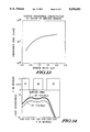
- a graph illustrates the doping concentration (phosphorus is used as an example) and the doping depth of a doped region as a function of opening size (for an illustration of opening size see "X" in FIG. 6 or FIG. 10).
- a 2.0 micron-wide window will create a doped region having a surface concentration (i.e. concentration at 0.0 micron depth) of 1.13 ⁇ 10 17 dopants/cm 3 and a doping depth of roughly 1.75 microns.
- Doping depth is arbitrarily defined in FIG. 12 as being the depth at which the doping concentration drops below 1 ⁇ 10 15 .
- a 1.0 micron-wide window will create a doped region having a surface concentration (i.e.
- a 0.5 micron-wide window will create a doped region having a surface concentration of 9.0 ⁇ 10 16 dopants/cm 3 and a doping depth of roughly 1.59 microns.
- a 0.4 micron-wide window will create a doped region having a surface concentration of 8.0 ⁇ 10 16 dopants/cm 3 and a doping depth of roughly 1.55 microns.
- a 0.3 micron-wide window will create a doped region having a surface concentration of 6.0 ⁇ 10 16 dopants/cm 3 and a doping depth of roughly 1.50 microns.
- FIG. 12 illustrates the vertical phosphorus profile at a center of a window implant region.
- FIG. 13 illustrates a graph of surface doping concentration versus window width "X".
- window width is decreased, the surface phosphorus concentration decreases in a logarithmic manner toward zero. More specifically, FIG. 13 illustrates the surface phosphorus concentration at the center of an implant window as a function of the window width.
- FIG. 14 graphically illustrates the lateral dopant uniformity of a doped region as a function of opening width and opening spacing.
- FIG. 14 illustrates a masking layer 14 having a plurality of openings. Each of the openings in the plurality of openings are roughly 0.4 micron in width and are spaced apart by roughly 0.8 micron.
- FIG. 14 illustrates that 0.4 micron openings separated by 0.8 micron spaces forms a doped region which varies laterally in surface doping concentration from roughly 3.0 ⁇ 10 16 to 9 ⁇ 10 16 in a lateral direction after a brief thermal cycle. Three different vertical depths are used to illustrate the doping concentration in FIG. 14.
- FIG. 15 graphically illustrates the lateral dopant uniformity of a doped region as a function of opening width and opening spacing.
- FIG. 15 illustrates a masking layer 14 having a plurality of openings. Each of the openings in the plurality of openings are roughly 0.4 micron in width and are spaced apart by roughly 0.4 micron.
- the pattern of masking layer 14 is continuos to the left of the X axis in FIG. 15.
- FIG. 15 illustrates that 0.4 micron openings separated by 0.4 micron spaces forms a doped region which does not vary significantly in doping concentration in a lateral direction after a brief thermal cycle. Three different vertical depths are used to illustrate the doping concentration in FIG. 15.
- FIG. 16 graphically illustrates the lateral dopant uniformity of a doped region as a function of opening width and opening spacing.
- FIG. 16 illustrates a masking layer 14 having a plurality of openings. Each of the openings in the plurality of openings are roughly 0.6 micron in width and are spaced apart by roughly 0.6 micron.
- the pattern of masking layer 14 is continuos to the left of the X axis in FIG. 16.
- FIG. 16 illustrates that 0.6 micron openings separated by 0.6 micron spaces forms a doped region which varies only slightly in doping concentration in a lateral direction after a brief thermal cycle. Three different vertical depths are used to illustrate the doping concentration in FIG. 16.
- FIGS. 14-16 collectively illustrate that spacing dimensions and spacing separation significantly influence lateral doping uniformity, doping concentration, and doped region junction depth.
- the mask and implant techniques taught herein may therefore be exactly constructed to form one or more doped regions or well regions each having a specific/different doping depth, a specific/different doping concentration, and a specific/different doping uniformity.
- FIGS. 17-18 illustrate that the inventive mask and implant technique taught herein may be used to form two or more buried layers having different doping concentrations.
- two or more doped regions i.e. well regions 24 and 26
- FIG. 17 is identical to FIG. 6.
- FIG. 18 illustrates that the masking layer 14 is removed.
- An epitaxial/selective growth step is used to form buried layers from the doped regions 24 and 26 via the formation of an epitaxial growth layer 100.
- the epitaxial growth layer 100 may be insitu doped, undoped, ion implanted, or the like.
- the buried layers may be formed, for example, as an N+ buried layer and an N buried layer combination or a P+ buried layer and a P buried layer combination.
- the epitaxial growth layer 100 is a semiconductive material and may be selectively grown or formed via a blanket growth process (i.e. a growth region is formed across the entire integrated circuit).
- both phosphorus and arsenic may be implanted to form diffusion regions with different diffusion characteristics.
- the masking layers taught herein are usually always cut in rectangular, checker board, or square patterns, but other geometries exist. Triangles, circles, grids, crossing lines, crosses, and other geometries may be used to pattern the masking layers taught herein.
- Other forms of lithography such as phase shifting, X-ray lithography, E-beam lithography, and the like may be used to form features within the masking layers.
- the doped regions formed herein may be used to form BiCMOS devices, microcontroller circuits, combined digital/analog circuits, memory arrays, and the like.
- a dielectric layer (not illustrated) may optionally be formed between the masking layer 14 and the substrate 12.
- An implant may then be performed through the dielectric layer (not illustrated) for an improved doping profile. Doping profile and doping concentration are both affected by the process described herein.
- this invention may be used to implant non-dopant atoms such as oxygen and nitrogen. This technique of implanting non-dopant atoms may be useful for selective implantation of oxygen (SIMOX) or nitrogen when different oxide or nitride thicknesses are useful.
- SIMOX selective implantation of oxygen
- this invention is not limited to the particular forms illustrated and that it is intended in the appended claims to cover all modifications that do not depart from the spirit and scope of this invention.
Abstract
Description
Claims (24)
Priority Applications (1)
| Application Number | Priority Date | Filing Date | Title |
|---|---|---|---|
| US07/982,164 US5300454A (en) | 1992-11-24 | 1992-11-24 | Method for forming doped regions within a semiconductor substrate |
Applications Claiming Priority (1)
| Application Number | Priority Date | Filing Date | Title |
|---|---|---|---|
| US07/982,164 US5300454A (en) | 1992-11-24 | 1992-11-24 | Method for forming doped regions within a semiconductor substrate |
Publications (1)
| Publication Number | Publication Date |
|---|---|
| US5300454A true US5300454A (en) | 1994-04-05 |
Family
ID=25528894
Family Applications (1)
| Application Number | Title | Priority Date | Filing Date |
|---|---|---|---|
| US07/982,164 Expired - Lifetime US5300454A (en) | 1992-11-24 | 1992-11-24 | Method for forming doped regions within a semiconductor substrate |
Country Status (1)
| Country | Link |
|---|---|
| US (1) | US5300454A (en) |
Cited By (19)
| Publication number | Priority date | Publication date | Assignee | Title |
|---|---|---|---|---|
| EP0755073A1 (en) * | 1995-07-18 | 1997-01-22 | Siemens Aktiengesellschaft | Method of producing semiconductor wells of different doping level |
| US5741732A (en) * | 1995-05-03 | 1998-04-21 | Sony Corporation | Method for detecting implantation mask misalignment |
| US6121659A (en) * | 1998-03-27 | 2000-09-19 | International Business Machines Corporation | Buried patterned conductor planes for semiconductor-on-insulator integrated circuit |
| EP1045461A2 (en) * | 1999-02-01 | 2000-10-18 | Sentron Ag | Method of making Hall-effect devices |
| US6146976A (en) * | 1997-03-05 | 2000-11-14 | Infineon Technology Ag | Method for producing bridged doped zones |
| US6200884B1 (en) * | 1999-07-31 | 2001-03-13 | Advanced Micro Devices, Inc. | Method for shaping photoresist mask to improve high aspect ratio ion implantation |
| US20030140844A1 (en) * | 2002-01-31 | 2003-07-31 | Maa Jer-Shen | Method to form thick relaxed SiGe Layer with trench structure |
| US20040147067A1 (en) * | 2002-10-24 | 2004-07-29 | Hitomi Ushitani | Semiconductor apparatus and method for manufacturing the same |
| EP1475837A1 (en) * | 2002-01-16 | 2004-11-10 | Sanken Electric Co., Ltd. | Semiconductor device manufacturing method |
| DE10325011A1 (en) * | 2003-06-03 | 2005-01-05 | Austriamicrosystems Ag | Manufacturing different depth doping regions in substrate involves implanting doping material through mask openings with doses controlled by shaping openings/stops, driving deeper into substrate |
| US7037814B1 (en) * | 2003-10-10 | 2006-05-02 | National Semiconductor Corporation | Single mask control of doping levels |
| US20060270203A1 (en) * | 2005-05-31 | 2006-11-30 | International Business Machines Corporation | Varied impurity profile region formation for varying breakdown voltage of devices |
| US20070155108A1 (en) * | 2004-02-24 | 2007-07-05 | Samsung Electronics Co., Ltd. | Doping mask and methods of manufacturing charge transfer image and microelectronic device using the same |
| US20090098718A1 (en) * | 2004-12-03 | 2009-04-16 | Martin Knaipp | Multiple mask and method for producing differently doped regions |
| US20120119265A1 (en) * | 2010-11-12 | 2012-05-17 | Taiwan Semiconductor Manufacturing Company, Ltd. | Source tip optimization for high voltage transistor devices |
| FR2977072A1 (en) * | 2011-06-27 | 2012-12-28 | St Microelectronics Crolles 2 | Method for doping silicon substrate, involves annealing semiconductor substrate to obtain doped zone extending below and on both sides of stud and having approximately homogeneous concentration of doping agents |
| US20150072480A1 (en) * | 2013-09-11 | 2015-03-12 | Taiwan Semiconductor Manufacturing Company Limited | Implant region definition |
| US20170110535A1 (en) * | 2015-10-20 | 2017-04-20 | Maxpower Semiconductor, Inc. | Vertical power transistor with thin bottom emitter layer and dopants implanted in trenches in shield area and termination rings |
| EP3742476A1 (en) * | 2019-05-20 | 2020-11-25 | Infineon Technologies AG | Method of implanting an implant species into a substrate at different depths |
Citations (7)
| Publication number | Priority date | Publication date | Assignee | Title |
|---|---|---|---|---|
| US3775192A (en) * | 1970-12-09 | 1973-11-27 | Philips Corp | Method of manufacturing semi-conductor devices |
| JPS53143179A (en) * | 1977-05-20 | 1978-12-13 | Nec Corp | Production of complementary type mos transistors |
| US4573257A (en) * | 1984-09-14 | 1986-03-04 | Motorola, Inc. | Method of forming self-aligned implanted channel-stop and buried layer utilizing non-single crystal alignment key |
| US4648174A (en) * | 1985-02-05 | 1987-03-10 | General Electric Company | Method of making high breakdown voltage semiconductor device |
| US4830981A (en) * | 1984-07-03 | 1989-05-16 | Texas Instruments Inc. | Trench capacitor process for high density dynamic ram |
| US4987089A (en) * | 1990-07-23 | 1991-01-22 | Micron Technology, Inc. | BiCMOS process and process for forming bipolar transistors on wafers also containing FETs |
| JPH03245525A (en) * | 1990-02-23 | 1991-11-01 | Fuji Electric Co Ltd | Manufacture of semiconductor device |
-
1992
- 1992-11-24 US US07/982,164 patent/US5300454A/en not_active Expired - Lifetime
Patent Citations (7)
| Publication number | Priority date | Publication date | Assignee | Title |
|---|---|---|---|---|
| US3775192A (en) * | 1970-12-09 | 1973-11-27 | Philips Corp | Method of manufacturing semi-conductor devices |
| JPS53143179A (en) * | 1977-05-20 | 1978-12-13 | Nec Corp | Production of complementary type mos transistors |
| US4830981A (en) * | 1984-07-03 | 1989-05-16 | Texas Instruments Inc. | Trench capacitor process for high density dynamic ram |
| US4573257A (en) * | 1984-09-14 | 1986-03-04 | Motorola, Inc. | Method of forming self-aligned implanted channel-stop and buried layer utilizing non-single crystal alignment key |
| US4648174A (en) * | 1985-02-05 | 1987-03-10 | General Electric Company | Method of making high breakdown voltage semiconductor device |
| JPH03245525A (en) * | 1990-02-23 | 1991-11-01 | Fuji Electric Co Ltd | Manufacture of semiconductor device |
| US4987089A (en) * | 1990-07-23 | 1991-01-22 | Micron Technology, Inc. | BiCMOS process and process for forming bipolar transistors on wafers also containing FETs |
Non-Patent Citations (2)
| Title |
|---|
| "A Buried N-Grid For Protection Against Radiation Induced Charge Collection in Electronic Circuits", Wordeman et al., 1981 IEEE IEDM '81, pp. 40-43. |
| A Buried N Grid For Protection Against Radiation Induced Charge Collection in Electronic Circuits , Wordeman et al., 1981 IEEE IEDM 81, pp. 40 43. * |
Cited By (38)
| Publication number | Priority date | Publication date | Assignee | Title |
|---|---|---|---|---|
| US5741732A (en) * | 1995-05-03 | 1998-04-21 | Sony Corporation | Method for detecting implantation mask misalignment |
| US5736445A (en) * | 1995-07-18 | 1998-04-07 | Siemens Aktiengesellschaft | Method for producing at least two transsistors in a semiconductor body |
| EP0755073A1 (en) * | 1995-07-18 | 1997-01-22 | Siemens Aktiengesellschaft | Method of producing semiconductor wells of different doping level |
| US6146976A (en) * | 1997-03-05 | 2000-11-14 | Infineon Technology Ag | Method for producing bridged doped zones |
| US6121659A (en) * | 1998-03-27 | 2000-09-19 | International Business Machines Corporation | Buried patterned conductor planes for semiconductor-on-insulator integrated circuit |
| EP1045461A2 (en) * | 1999-02-01 | 2000-10-18 | Sentron Ag | Method of making Hall-effect devices |
| EP1045461A3 (en) * | 1999-02-01 | 2005-02-09 | Sentron Ag | Method of making Hall-effect devices |
| US6200884B1 (en) * | 1999-07-31 | 2001-03-13 | Advanced Micro Devices, Inc. | Method for shaping photoresist mask to improve high aspect ratio ion implantation |
| EP1475837A1 (en) * | 2002-01-16 | 2004-11-10 | Sanken Electric Co., Ltd. | Semiconductor device manufacturing method |
| EP1475837A4 (en) * | 2002-01-16 | 2007-11-28 | Sanken Electric Co Ltd | Semiconductor device manufacturing method |
| US7226504B2 (en) * | 2002-01-31 | 2007-06-05 | Sharp Laboratories Of America, Inc. | Method to form thick relaxed SiGe layer with trench structure |
| US20030140844A1 (en) * | 2002-01-31 | 2003-07-31 | Maa Jer-Shen | Method to form thick relaxed SiGe Layer with trench structure |
| US7405111B2 (en) * | 2002-10-24 | 2008-07-29 | Semiconductor Energy Laboratory Co., Ltd. | Methods for manufacturing an active matrix display device |
| US7683372B2 (en) | 2002-10-24 | 2010-03-23 | Semiconductor Energy Laboratory Co., Ltd | Semiconductor apparatus and method for manufacturing the same |
| US20040147067A1 (en) * | 2002-10-24 | 2004-07-29 | Hitomi Ushitani | Semiconductor apparatus and method for manufacturing the same |
| US20090039430A1 (en) * | 2002-10-24 | 2009-02-12 | Semiconductor Energy Laboratory Co., Ltd. | Semiconductor apparatus and method for manufacturing the same |
| DE10325011B4 (en) * | 2003-06-03 | 2007-09-27 | Austriamicrosystems Ag | Method for producing differently deep doping regions in a substrate |
| DE10325011A1 (en) * | 2003-06-03 | 2005-01-05 | Austriamicrosystems Ag | Manufacturing different depth doping regions in substrate involves implanting doping material through mask openings with doses controlled by shaping openings/stops, driving deeper into substrate |
| US7037814B1 (en) * | 2003-10-10 | 2006-05-02 | National Semiconductor Corporation | Single mask control of doping levels |
| US20070155108A1 (en) * | 2004-02-24 | 2007-07-05 | Samsung Electronics Co., Ltd. | Doping mask and methods of manufacturing charge transfer image and microelectronic device using the same |
| US7595518B2 (en) * | 2004-02-24 | 2009-09-29 | Samsung Electronics Co., Ltd. | Doping mask and methods of manufacturing charge transfer image and microelectronic device using the same |
| US20090098718A1 (en) * | 2004-12-03 | 2009-04-16 | Martin Knaipp | Multiple mask and method for producing differently doped regions |
| US7820342B2 (en) | 2004-12-03 | 2010-10-26 | Austriamicrosystems Ag | Multiple mask and method for producing differently doped regions |
| US8030167B2 (en) | 2005-05-31 | 2011-10-04 | International Business Machines Corporation | Varied impurity profile region formation for varying breakdown voltage of devices |
| US7550787B2 (en) | 2005-05-31 | 2009-06-23 | International Business Machines Corporation | Varied impurity profile region formation for varying breakdown voltage of devices |
| US20060270203A1 (en) * | 2005-05-31 | 2006-11-30 | International Business Machines Corporation | Varied impurity profile region formation for varying breakdown voltage of devices |
| CN102468179B (en) * | 2010-11-12 | 2014-05-21 | 台湾积体电路制造股份有限公司 | semiconductor device and method thereof |
| CN102468179A (en) * | 2010-11-12 | 2012-05-23 | 台湾积体电路制造股份有限公司 | semiconductor device and method thereof |
| US8629026B2 (en) * | 2010-11-12 | 2014-01-14 | Taiwan Semiconductor Manufacturing Company, Ltd. | Source tip optimization for high voltage transistor devices |
| US20120119265A1 (en) * | 2010-11-12 | 2012-05-17 | Taiwan Semiconductor Manufacturing Company, Ltd. | Source tip optimization for high voltage transistor devices |
| US9331195B2 (en) | 2010-11-12 | 2016-05-03 | Taiwan Semiconductor Manufacturing Company, Ltd. | Source tip optimization for high voltage transistor devices which includes a P-body extension region |
| FR2977072A1 (en) * | 2011-06-27 | 2012-12-28 | St Microelectronics Crolles 2 | Method for doping silicon substrate, involves annealing semiconductor substrate to obtain doped zone extending below and on both sides of stud and having approximately homogeneous concentration of doping agents |
| US20150072480A1 (en) * | 2013-09-11 | 2015-03-12 | Taiwan Semiconductor Manufacturing Company Limited | Implant region definition |
| US9087773B2 (en) * | 2013-09-11 | 2015-07-21 | Taiwan Semiconductor Manufacturing Company Limited | Implant region definition |
| US20170110535A1 (en) * | 2015-10-20 | 2017-04-20 | Maxpower Semiconductor, Inc. | Vertical power transistor with thin bottom emitter layer and dopants implanted in trenches in shield area and termination rings |
| US9825128B2 (en) * | 2015-10-20 | 2017-11-21 | Maxpower Semiconductor, Inc. | Vertical power transistor with thin bottom emitter layer and dopants implanted in trenches in shield area and termination rings |
| EP3742476A1 (en) * | 2019-05-20 | 2020-11-25 | Infineon Technologies AG | Method of implanting an implant species into a substrate at different depths |
| US11640908B2 (en) | 2019-05-20 | 2023-05-02 | Infineon Technologies Ag | Method of implanting an implant species into a substrate at different depths |
Similar Documents
| Publication | Publication Date | Title |
|---|---|---|
| US5300454A (en) | Method for forming doped regions within a semiconductor substrate | |
| US4784971A (en) | Process for manufacturing semiconductor BICMOS device | |
| JP3301062B2 (en) | High performance MOSFET device with raised source and drain and method of forming the same | |
| US5219784A (en) | Spacer formation in a bicmos device | |
| US6790781B2 (en) | Dual depth trench isolation | |
| US5021354A (en) | Process for manufacturing a semiconductor device | |
| US6040208A (en) | Angled ion implantation for selective doping | |
| US6180441B1 (en) | Bar field effect transistor | |
| US5943576A (en) | Angled implant to build MOS transistors in contact holes | |
| US6027963A (en) | Method and mask structure for self-aligning ion implanting to form various device structures | |
| US5154946A (en) | CMOS structure fabrication | |
| JPS63263766A (en) | Manufacture of bipolar transistor device | |
| KR970011641B1 (en) | Semiconductor device and method of manufacturing the same | |
| US6249025B1 (en) | Using epitaxially grown wells for reducing junction capacitances | |
| US6362025B1 (en) | Method of manufacturing a vertical-channel MOSFET | |
| US5627091A (en) | Mask ROM process for making a ROM with a trench shaped channel | |
| JPH02278761A (en) | Manufacture of cmos and bipolar transistor using selective epitaxial growth facilitating contraction to less than 0.5 micron | |
| US6069384A (en) | Integrated circuit including vertical transistors with spacer gates having selected gate widths | |
| EP0036499A1 (en) | A polysilicon-base self-aligned bipolar transistor process | |
| EP0487937B1 (en) | A semiconductor device having punch-through protected buried contacts and method for making the same | |
| EP0589631B1 (en) | Method for recessed, self aligned, low base resistance structure | |
| EP0959497B1 (en) | A method of forming an ultra-thin soi electrostatic discharge protection device | |
| JPH04258160A (en) | Semiconductor device | |
| KR0179823B1 (en) | Manufacture for semiconductor device | |
| JPH05160401A (en) | Mos transistor |
Legal Events
| Date | Code | Title | Description |
|---|---|---|---|
| AS | Assignment |
Owner name: MOTOROLA, INC., ILLINOIS Free format text: ASSIGNMENT OF ASSIGNORS INTEREST.;ASSIGNORS:TAFT, ROBERT C.;SUBRAHMANYAN, RAVI;REEL/FRAME:006346/0997 Effective date: 19921120 |
|
| STCF | Information on status: patent grant |
Free format text: PATENTED CASE |
|
| FPAY | Fee payment |
Year of fee payment: 4 |
|
| FPAY | Fee payment |
Year of fee payment: 8 |
|
| AS | Assignment |
Owner name: FREESCALE SEMICONDUCTOR, INC., TEXAS Free format text: ASSIGNMENT OF ASSIGNORS INTEREST;ASSIGNOR:MOTOROLA, INC.;REEL/FRAME:015698/0657 Effective date: 20040404 Owner name: FREESCALE SEMICONDUCTOR, INC.,TEXAS Free format text: ASSIGNMENT OF ASSIGNORS INTEREST;ASSIGNOR:MOTOROLA, INC.;REEL/FRAME:015698/0657 Effective date: 20040404 |
|
| FPAY | Fee payment |
Year of fee payment: 12 |
|
| AS | Assignment |
Owner name: CITIBANK, N.A. AS COLLATERAL AGENT, NEW YORK Free format text: SECURITY AGREEMENT;ASSIGNORS:FREESCALE SEMICONDUCTOR, INC.;FREESCALE ACQUISITION CORPORATION;FREESCALE ACQUISITION HOLDINGS CORP.;AND OTHERS;REEL/FRAME:018855/0129 Effective date: 20061201 Owner name: CITIBANK, N.A. AS COLLATERAL AGENT,NEW YORK Free format text: SECURITY AGREEMENT;ASSIGNORS:FREESCALE SEMICONDUCTOR, INC.;FREESCALE ACQUISITION CORPORATION;FREESCALE ACQUISITION HOLDINGS CORP.;AND OTHERS;REEL/FRAME:018855/0129 Effective date: 20061201 |
|
| AS | Assignment |
Owner name: CITIBANK, N.A., AS COLLATERAL AGENT,NEW YORK Free format text: SECURITY AGREEMENT;ASSIGNOR:FREESCALE SEMICONDUCTOR, INC.;REEL/FRAME:024397/0001 Effective date: 20100413 Owner name: CITIBANK, N.A., AS COLLATERAL AGENT, NEW YORK Free format text: SECURITY AGREEMENT;ASSIGNOR:FREESCALE SEMICONDUCTOR, INC.;REEL/FRAME:024397/0001 Effective date: 20100413 |
|
| AS | Assignment |
Owner name: ZOZO MANAGEMENT, LLC, DELAWARE Free format text: ASSIGNMENT OF ASSIGNORS INTEREST;ASSIGNOR:FREESCALE SEMICONDUCTOR, INC.;REEL/FRAME:034034/0236 Effective date: 20120814 |
|
| AS | Assignment |
Owner name: APPLE INC., CALIFORNIA Free format text: ASSIGNMENT OF ASSIGNORS INTEREST;ASSIGNOR:ZOZO MANAGEMENT, LLC;REEL/FRAME:034732/0019 Effective date: 20141219 |
|
| AS | Assignment |
Owner name: FREESCALE SEMICONDUCTOR, INC., TEXAS Free format text: PATENT RELEASE;ASSIGNOR:CITIBANK, N.A., AS COLLATERAL AGENT;REEL/FRAME:037354/0225 Effective date: 20151207 Owner name: FREESCALE SEMICONDUCTOR, INC., TEXAS Free format text: PATENT RELEASE;ASSIGNOR:CITIBANK, N.A., AS COLLATERAL AGENT;REEL/FRAME:037356/0553 Effective date: 20151207 Owner name: FREESCALE SEMICONDUCTOR, INC., TEXAS Free format text: PATENT RELEASE;ASSIGNOR:CITIBANK, N.A., AS COLLATERAL AGENT;REEL/FRAME:037356/0143 Effective date: 20151207 |