US5148535A - Non-bus request refresh system for shortening refresh timing - Google Patents
Non-bus request refresh system for shortening refresh timing Download PDFInfo
- Publication number
- US5148535A US5148535A US07/401,343 US40134389A US5148535A US 5148535 A US5148535 A US 5148535A US 40134389 A US40134389 A US 40134389A US 5148535 A US5148535 A US 5148535A
- Authority
- US
- United States
- Prior art keywords
- signal
- cpu
- latch
- memory
- input
- Prior art date
- Legal status (The legal status is an assumption and is not a legal conclusion. Google has not performed a legal analysis and makes no representation as to the accuracy of the status listed.)
- Expired - Lifetime
Links
- 238000004904 shortening Methods 0.000 title 1
- 230000003111 delayed effect Effects 0.000 claims description 8
- 238000000034 method Methods 0.000 claims description 2
- 238000001514 detection method Methods 0.000 claims 3
- 230000007704 transition Effects 0.000 description 13
- 238000010586 diagram Methods 0.000 description 8
- 101100219315 Arabidopsis thaliana CYP83A1 gene Proteins 0.000 description 5
- 101100269674 Mus musculus Alyref2 gene Proteins 0.000 description 5
- 101100140580 Saccharomyces cerevisiae (strain ATCC 204508 / S288c) REF2 gene Proteins 0.000 description 5
- 101100152598 Arabidopsis thaliana CYP73A5 gene Proteins 0.000 description 4
- 230000007423 decrease Effects 0.000 description 1
- 230000006870 function Effects 0.000 description 1
- 230000000977 initiatory effect Effects 0.000 description 1
- 239000007787 solid Substances 0.000 description 1
Images


Classifications
-
- G—PHYSICS
- G11—INFORMATION STORAGE
- G11C—STATIC STORES
- G11C11/00—Digital stores characterised by the use of particular electric or magnetic storage elements; Storage elements therefor
- G11C11/21—Digital stores characterised by the use of particular electric or magnetic storage elements; Storage elements therefor using electric elements
- G11C11/34—Digital stores characterised by the use of particular electric or magnetic storage elements; Storage elements therefor using electric elements using semiconductor devices
- G11C11/40—Digital stores characterised by the use of particular electric or magnetic storage elements; Storage elements therefor using electric elements using semiconductor devices using transistors
- G11C11/401—Digital stores characterised by the use of particular electric or magnetic storage elements; Storage elements therefor using electric elements using semiconductor devices using transistors forming cells needing refreshing or charge regeneration, i.e. dynamic cells
- G11C11/406—Management or control of the refreshing or charge-regeneration cycles
-
- G—PHYSICS
- G06—COMPUTING; CALCULATING OR COUNTING
- G06F—ELECTRIC DIGITAL DATA PROCESSING
- G06F13/00—Interconnection of, or transfer of information or other signals between, memories, input/output devices or central processing units
- G06F13/14—Handling requests for interconnection or transfer
- G06F13/16—Handling requests for interconnection or transfer for access to memory bus
- G06F13/1605—Handling requests for interconnection or transfer for access to memory bus based on arbitration
- G06F13/161—Handling requests for interconnection or transfer for access to memory bus based on arbitration with latency improvement
- G06F13/1636—Handling requests for interconnection or transfer for access to memory bus based on arbitration with latency improvement using refresh
Definitions
- the present invention relates generally to digital computers having memory and I/O including dynamic memory and, more particularly, relates to a system for reducing the time required to refresh the dynamic memory.
- a separate timer functions to generate a refresh request signal at specified intervals determined by the refresh requirements of the dynamic memory.
- a refresh system requests the bus from the CPU and puts the CPU in a wait state while the refresh operation is completed.
- the refresh interval is about 15 microseconds. One row of memory is refreshed every refresh interval.
- Typical refresh systems utilize a DMA controller so that cycles required for arbitration are utilized in addition to the cycles required to refresh the memory.
- a standard PC-XT using the standard refresh system consumes about 2.5 microseconds or about 17% of each refresh interval.
- a PC-AT type computer also extends the time consumed for refresh by requiring extra cycles for arbitration.
- the standard refresh system significantly reduces the usable portion of the CPU cycle time and decreases the effective speed of the computer.
- the present invention is a refresh system and method that does not request the bus from the CPU.
- a first signal indicating the end of a CPU bus cycle is monitored and the refresh operation is initiated when a CPU bus cycle terminates.
- the status and address signals generated by the CPU are stored.
- the stored status signal is transferred to the bus controller upon completion of the refresh operation to start a delayed bus cycle.
- the state of the first signal is controlled so that a new CPU bus cycle is not started until the delayed CPU bus cycle is completed.
- the invention reduces the unavailability of the bus to the minimum time actually required to perform the refresh operation.
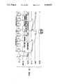
- FIG. 1 is a block diagram of a preferred embodiment of the invention:
- FIG. 2 is a timing diagram depicting a illustrating CPU bus cycle:
- FIG. 3 is a state diagram illustrating the operation of the embodiment of FIG. 1;
- FIGS. 4 and 5 are timing diagrams illustrating the operation of the embodiment of FIG. 1.
- FIG. 1 is a block diagram of an embodiment of the invention. The operation of this embodiment will be described referring the timing of level transitions of several signals. The symbols utilized to describe these signal and descriptions of the signals are presented in the following table:
- FIG. 1 several elements are standard parts included in the bus and bus control system of PC type computers utilizing a microprocessor CPU 8, such as an INTEL 80286 having S0, S1, BHE, AO-14 A21, and MIO signal outputs.
- the CPU COMMAND BUS CONTROLLER 10 such as an INTEL model 82288, receives the S0, S1 signals, generates the MEMWR, IORD, and IOWR signal, and includes logic for pulling the READY signal low when a CPU bus cycle is completed.
- the address latch 12, row/column address mux 14, and programmable interval timer (PIT) 16 which sets REFREQ are standard PC-XT components utilized by the present system.
- a unique REFRESH STATE MACHINE 20 has inputs for receiving the REFREQ signal asserted by the PIT 16, the status bits S0, S1 generated by the CPU 8. and the READY signal set by the ready logic.
- the REFRESH STATE MACHINE 20 includes REFMRD. STATSEL. STATALE, EALE, REFRESH, REFAEN, and READY output ports.
- the REFRESH STATE MACHINE 20 receives the READY signal asserted by the READY logic and also has the capability to prevent the READY signal form being pulled low by the READY logic.
- a REF LATCH 22 receives S0, S1 at its data input and STATALE at is clock input and a REF MUX 22 has a first data input that receives S0, S1 directly from the CPU 8, a second data input that receives the output from the REF LATCH 22, and a select input that receives STATSEL.
- An E ADR LATCH 26 receives the BHE, AO-A21, and MIO signals from the microprocessor CPU 8 at it data inputs and the EALE signal at its clock input, the REF COUNTER 28, receives refresh signal at is start input, and a REF ADR BUFFER 30 receives the REF COUNTER count signal at its data input.
- the output enable (OE) input of the REF ADR BUFFER 30 receives the REFAEN signal, the OE input of the E ADR LATCH, and the OE input of the REF LATCH 22 receive the REFAEN signal inverted by an invertor 32.
- FIG. 2 is a diagram of the CPU bus cycle. The details of the bus cycle are well known in the art and only those features relevant to the present invention are described.
- the first state is a Ts state which is signalled by the S0, S1 signal going low.
- Ts state the address signals and, for a write operation, data signals are generated by the microprocessor CPU 8.
- Tc command state
- the memory or I/O device either transfer read data to the microprocessor CPU 8 or accept write data.
- the Tc states are repeated until the READY signal is reset and goes low.
- the bus cycle can be extended by delaying the READY transition from high to low. This READY signal transition signals the end of the current bus cycle.
- the standard refresh cycle requires the use of the bus for a time interval of four T states and prevents the use of the CPU during this interval.
- FIG. 3 is a state diagram where the labeled circles indicate the various states of the REFRESH STATE MACHINE 20, the solid arrows indicate transitions between the states, and the dotted arrows are labelled by the signal that causes a state transition.
- FIGS. 4 and 5 are timing diagrams depicting the signal transitions that occur during state transitions and the timing thereof.
- the operation of the system of FIG. 1 will now be described with reference to FIGS. 1-5.
- the transition from the IDLE STATE 50 to the REFl STATE 60 is caused by the low to high transition of REFREQ.
- the REFRESH STATE MACHINE then monitors READY to determine the end of a CPU bus cycle and makes the transition to the REF2 STATE 70.
- FIG. 4 illustrates the timing of the refresh operation if the CPU 8 does not assert S0, S1 to request the bus during the refresh operation.
- REFRESH. REFMRD. and REFAEN are set to increment the refresh counter 28 to generate the next row address required for the refresh operation, to provide the required READ signal to the DRAMS being refreshed, and to enable the refresh buffer 30 to drive the refresh address generated by the refresh counter 28 respectively.
- the transition from the REF2 STATE 70 to the IDLE STATE 50 occurs after the four T-states required to refresh the addressed memory row.
- FIG. 6 depicts the state of the signals when the CPU 8 requests the bus during the REF2 STATE before the completion of the refresh operation.
- the refresh operation occurs during T-states C3 to C6.
- the assertion of S0, S1, ADR 0-21, and MIO by the CPU 8 at cycle C4 indicates the beginning of a new CPU bus cycle.
- the REFRESH STATE MACHINE 20 detects the assertion of S0, S1 and makes the transition from the REF2 STATE 70 to the REF3 STATE 80 at T-state C4.
- the assertion of the status bits S0, S1 signals the beginning of a Ts state where status and address data are output from the CPU 8.
- REF3 STATE 80 STATALE is set, after a required set-up time, to latch S0, S1 into the REF LATCH 22, EALE is set, after a required set-up time, to latch AO-A21.
- BHE and MIO into the E LATCH 26, and STATSEL is set to couple the second input of REF MUX 24 to the BUS CONTROLLER 10.
- REFAEN is set during T-states C5 and C6 of the REF3 STATE 80 so that the outputs of the REF LATCH 22 and E LATCH 26 are not enabled and their outputs are in the high impedance state.
- the latched status, control, and address data for the newly initiated CPU bus is not transferred to the BC 10 or buses until the refresh operation is completed.
- the BC 10 responds to the latched S0, S1 signals to generate the required control signals to complete the CPU bus cycle that was initiated during the REF3 STATE 80.
- the READY signal is held high by the REFRESH STATE MACHINE 20 during cycles C7 and C8 to prevent the CPU 8 from initiating a new cycle until the delayed cycle is completed, the transition to the IDLE STATE 50 occurs when READY is reset.
- the present system reduces the bus availability only by the amount of time actually required by the refresh operation and achieves a substantial reduction of the amount of time the bus is unavailable to the CPU.
- the refresh operation requires the bus for only 5 microseconds.
- control signals generated by the REFRESH STATE MACHINE 20 are derived from standard control signals generated by the CPU and other hardware in a PC-XT type of computer.
- the particular digital circuitry required to implement the timing of the control signals generated by the REFRESH STATE MACHINE includes gates, flip-flops, and other circuitry which is standard and not part of the invention. Persons of ordinary skill in the art, apprised of the information disclosed herein, may implement such digital circuitry in various ways. Accordingly, the invention is not intended to be limited except as provided by the appended claims.
Abstract
Description
______________________________________
SIGNAL NAME     SIGNAL DESCRIPTION
______________________________________
S0,S1           Status Bits
BHE             Bus High Enable
A0-A21          Address Bits
MIO             Memory I/O
MEMRD           Memory Read
MEMWR           Memory Write
IORD            I/O Read
IOWR            I/O Write
READY           Ready
REFREQ          Refresh Request
REFMRD          Refresh Memory Read
STATSEL         State Machine Select
STATALE         State Machine Address
                Latch Enable
REFRESH         Refresh
REFAEN          Refresh Address Latch
                Enable
EALE            E Address Latch Enable
______________________________________
Claims (3)
Priority Applications (1)
| Application Number | Priority Date | Filing Date | Title |
|---|---|---|---|
| US07/401,343 US5148535A (en) | 1989-08-31 | 1989-08-31 | Non-bus request refresh system for shortening refresh timing |
Applications Claiming Priority (1)
| Application Number | Priority Date | Filing Date | Title |
|---|---|---|---|
| US07/401,343 US5148535A (en) | 1989-08-31 | 1989-08-31 | Non-bus request refresh system for shortening refresh timing |
Publications (1)
| Publication Number | Publication Date |
|---|---|
| US5148535A true US5148535A (en) | 1992-09-15 |
Family
ID=23587366
Family Applications (1)
| Application Number | Title | Priority Date | Filing Date |
|---|---|---|---|
| US07/401,343 Expired - Lifetime US5148535A (en) | 1989-08-31 | 1989-08-31 | Non-bus request refresh system for shortening refresh timing |
Country Status (1)
| Country | Link |
|---|---|
| US (1) | US5148535A (en) |
Cited By (8)
| Publication number | Priority date | Publication date | Assignee | Title |
|---|---|---|---|---|
| EP0588250A2 (en) * | 1992-09-18 | 1994-03-23 | New Media Corporation | PSRAM refresh controller |
| US5305277A (en) * | 1991-04-24 | 1994-04-19 | International Business Machines Corporation | Data processing apparatus having address decoder supporting wide range of operational frequencies |
| US5305283A (en) * | 1990-04-06 | 1994-04-19 | Mosaid, Inc. | Dram column address latching technique |
| US5345574A (en) * | 1990-05-15 | 1994-09-06 | Seiko Epson Corporation | Memory card having controller providing adjustable refresh to a plurality of DRAMs |
| US5479642A (en) * | 1992-10-01 | 1995-12-26 | Digital Equipment Corporation | Method for maintaining low-overhead and non-coherent cache refresh mechanism with valid status monitoring on time period basis |
| WO1999014902A1 (en) * | 1997-09-17 | 1999-03-25 | Sony Electronics Inc. | Memory controller in a multi-port bridge for a local area network |
| FR2773634A1 (en) * | 1998-01-15 | 1999-07-16 | Sgs Thomson Microelectronics | Dynamic random access memory refreshment technique |
| US20210326278A1 (en) * | 2019-07-10 | 2021-10-21 | Silicon Motion, Inc. | Apparatus and method and computer program product for executing host input-output commands |
Citations (4)
| Publication number | Priority date | Publication date | Assignee | Title |
|---|---|---|---|---|
| US4649511A (en) * | 1983-07-25 | 1987-03-10 | General Electric Company | Dynamic memory controller for single-chip microprocessor |
| US4884234A (en) * | 1987-06-29 | 1989-11-28 | Ncr Corporation | Dynamic RAM refresh circuit with DMA access |
| US4924381A (en) * | 1984-06-11 | 1990-05-08 | Nec Corporation | Microprocessor having a dynamic memory refresh circuit |
| US4956820A (en) * | 1987-03-11 | 1990-09-11 | Texas Instruments Incorporated | Arbiter circuit for establishing priority control of read, write and refresh operations with respect to memory array |
-
1989
- 1989-08-31 US US07/401,343 patent/US5148535A/en not_active Expired - Lifetime
Patent Citations (4)
| Publication number | Priority date | Publication date | Assignee | Title |
|---|---|---|---|---|
| US4649511A (en) * | 1983-07-25 | 1987-03-10 | General Electric Company | Dynamic memory controller for single-chip microprocessor |
| US4924381A (en) * | 1984-06-11 | 1990-05-08 | Nec Corporation | Microprocessor having a dynamic memory refresh circuit |
| US4956820A (en) * | 1987-03-11 | 1990-09-11 | Texas Instruments Incorporated | Arbiter circuit for establishing priority control of read, write and refresh operations with respect to memory array |
| US4884234A (en) * | 1987-06-29 | 1989-11-28 | Ncr Corporation | Dynamic RAM refresh circuit with DMA access |
Cited By (9)
| Publication number | Priority date | Publication date | Assignee | Title |
|---|---|---|---|---|
| US5305283A (en) * | 1990-04-06 | 1994-04-19 | Mosaid, Inc. | Dram column address latching technique |
| US5345574A (en) * | 1990-05-15 | 1994-09-06 | Seiko Epson Corporation | Memory card having controller providing adjustable refresh to a plurality of DRAMs |
| US5305277A (en) * | 1991-04-24 | 1994-04-19 | International Business Machines Corporation | Data processing apparatus having address decoder supporting wide range of operational frequencies |
| EP0588250A2 (en) * | 1992-09-18 | 1994-03-23 | New Media Corporation | PSRAM refresh controller |
| EP0588250A3 (en) * | 1992-09-18 | 1994-11-30 | New Media Corp | PSRAM refresh controller. |
| US5479642A (en) * | 1992-10-01 | 1995-12-26 | Digital Equipment Corporation | Method for maintaining low-overhead and non-coherent cache refresh mechanism with valid status monitoring on time period basis |
| WO1999014902A1 (en) * | 1997-09-17 | 1999-03-25 | Sony Electronics Inc. | Memory controller in a multi-port bridge for a local area network |
| FR2773634A1 (en) * | 1998-01-15 | 1999-07-16 | Sgs Thomson Microelectronics | Dynamic random access memory refreshment technique |
| US20210326278A1 (en) * | 2019-07-10 | 2021-10-21 | Silicon Motion, Inc. | Apparatus and method and computer program product for executing host input-output commands |
Similar Documents
| Publication | Publication Date | Title |
|---|---|---|
| US6073223A (en) | Memory controller and method for intermittently activating and idling a clock signal for a synchronous memory | |
| US6457095B1 (en) | Method and apparatus for synchronizing dynamic random access memory exiting from a low power state | |
| KR100329344B1 (en) | Power management apparatus and method | |
| US7506126B2 (en) | Detection circuit for mixed asynchronous and synchronous memory operation | |
| US5873114A (en) | Integrated processor and memory control unit including refresh queue logic for refreshing DRAM during idle cycles | |
| EP1163598B1 (en) | Microprocessing device having programmable wait states | |
| TWI468926B (en) | Processor power management and method | |
| US5630145A (en) | Method and apparatus for reducing power consumption according to bus activity as determined by bus access times | |
| US20090161468A1 (en) | Semiconductor memory, memory system, and memory access control method | |
| US6079022A (en) | Method and apparatus for dynamically adjusting the clock speed of a bus depending on bus activity | |
| US5418920A (en) | Refresh control method and system including request and refresh counters and priority arbitration circuitry | |
| US6519689B2 (en) | Method and system for processing pipelined memory commands | |
| US5500827A (en) | Method and apparatus for improved DRAM refresh operation | |
| US5530944A (en) | Intelligent programmable dram interface timing controller | |
| US5579492A (en) | Data processing system and a method for dynamically ignoring bus transfer termination control signals for a predetermined amount of time | |
| US5148535A (en) | Non-bus request refresh system for shortening refresh timing | |
| US6232820B1 (en) | Method and apparatus for dynamic clock gating | |
| US5857082A (en) | Method and apparatus for quickly transferring data from a first bus to a second bus | |
| JP3728468B2 (en) | Memory control device | |
| US20050198542A1 (en) | Method and apparatus for a variable memory enable deassertion wait time | |
| US5893917A (en) | Memory controller and method of closing a page of system memory | |
| KR100432700B1 (en) | A self-synchronizing method and apparatus for exiting dynamic random access memory from a low power state | |
| US5680591A (en) | Method and apparatus for monitoring a row address strobe signal in a graphics controller | |
| US6047336A (en) | Speculative direct memory access transfer between slave devices and memory | |
| US7069363B1 (en) | On-chip bus |
Legal Events
| Date | Code | Title | Description |
|---|---|---|---|
| AS | Assignment |
Owner name: TANDY CORPORATION, TEXAS Free format text: ASSIGNMENT OF ASSIGNORS INTEREST.;ASSIGNOR:BALLARD, JERRY L.;REEL/FRAME:005118/0649 Effective date: 19890825 |
|
| STCF | Information on status: patent grant |
Free format text: PATENTED CASE |
|
| AS | Assignment |
Owner name: AST RESEARCH, INC., CALIFORNIA Free format text: ASSIGNMENT OF ASSIGNORS INTEREST;ASSIGNOR:TANDY CORPORATION AND ITS RADIO SHACK DIVISION;REEL/FRAME:006847/0109 Effective date: 19940103 |
|
| AS | Assignment |
Owner name: BANK OF AMERICA NATIONAL TRUST AND SAVINGS ASSOCIA Free format text: SECURITY INTEREST;ASSIGNOR:AST RESEARCH, INC., A DELAWARE CORPORATION;REEL/FRAME:007288/0234 Effective date: 19941223 |
|
| AS | Assignment |
Owner name: AST RESEARCH, INC., CALIFORNIA Free format text: RELEASE BY SECURED PARTY;ASSIGNOR:BANK OF AMERICA NATIONAL TRUST AND SAVINGS ASSOCIATION;REEL/FRAME:007492/0165 Effective date: 19950901 |
|
| FPAY | Fee payment |
Year of fee payment: 4 |
|
| AS | Assignment |
Owner name: SAMSUNG ELECTRONICS CO., LTD., KOREA, REPUBLIC OF Free format text: ASSIGNMENT OF ASSIGNORS INTEREST;ASSIGNOR:AST RESEARCH, INC.;REEL/FRAME:009942/0242 Effective date: 19990421 |
|
| FPAY | Fee payment |
Year of fee payment: 8 |
|
| FEPP | Fee payment procedure |
Free format text: PAYOR NUMBER ASSIGNED (ORIGINAL EVENT CODE: ASPN); ENTITY STATUS OF PATENT OWNER: LARGE ENTITY |
|
| FPAY | Fee payment |
Year of fee payment: 12 |