US4994896A - Semiconductor device - Google Patents
Semiconductor device Download PDFInfo
- Publication number
- US4994896A US4994896A US07/194,944 US19494488A US4994896A US 4994896 A US4994896 A US 4994896A US 19494488 A US19494488 A US 19494488A US 4994896 A US4994896 A US 4994896A
- Authority
- US
- United States
- Prior art keywords
- package
- external lead
- lead terminals
- semiconductor
- semiconductor package
- Prior art date
- Legal status (The legal status is an assumption and is not a legal conclusion. Google has not performed a legal analysis and makes no representation as to the accuracy of the status listed.)
- Expired - Lifetime
Links
Images


Classifications
-
- H—ELECTRICITY
- H01—ELECTRIC ELEMENTS
- H01L—SEMICONDUCTOR DEVICES NOT COVERED BY CLASS H10
- H01L23/00—Details of semiconductor or other solid state devices
- H01L23/48—Arrangements for conducting electric current to or from the solid state body in operation, e.g. leads, terminal arrangements ; Selection of materials therefor
- H01L23/488—Arrangements for conducting electric current to or from the solid state body in operation, e.g. leads, terminal arrangements ; Selection of materials therefor consisting of soldered or bonded constructions
- H01L23/495—Lead-frames or other flat leads
- H01L23/49541—Geometry of the lead-frame
- H01L23/49548—Cross section geometry
- H01L23/49551—Cross section geometry characterised by bent parts
- H01L23/49555—Cross section geometry characterised by bent parts the bent parts being the outer leads
-
- H—ELECTRICITY
- H05—ELECTRIC TECHNIQUES NOT OTHERWISE PROVIDED FOR
- H05K—PRINTED CIRCUITS; CASINGS OR CONSTRUCTIONAL DETAILS OF ELECTRIC APPARATUS; MANUFACTURE OF ASSEMBLAGES OF ELECTRICAL COMPONENTS
- H05K1/00—Printed circuits
- H05K1/18—Printed circuits structurally associated with non-printed electric components
- H05K1/181—Printed circuits structurally associated with non-printed electric components associated with surface mounted components
-
- H—ELECTRICITY
- H01—ELECTRIC ELEMENTS
- H01L—SEMICONDUCTOR DEVICES NOT COVERED BY CLASS H10
- H01L2224/00—Indexing scheme for arrangements for connecting or disconnecting semiconductor or solid-state bodies and methods related thereto as covered by H01L24/00
- H01L2224/01—Means for bonding being attached to, or being formed on, the surface to be connected, e.g. chip-to-package, die-attach, "first-level" interconnects; Manufacturing methods related thereto
- H01L2224/42—Wire connectors; Manufacturing methods related thereto
- H01L2224/47—Structure, shape, material or disposition of the wire connectors after the connecting process
- H01L2224/48—Structure, shape, material or disposition of the wire connectors after the connecting process of an individual wire connector
- H01L2224/4805—Shape
- H01L2224/4809—Loop shape
- H01L2224/48091—Arched
-
- H—ELECTRICITY
- H01—ELECTRIC ELEMENTS
- H01L—SEMICONDUCTOR DEVICES NOT COVERED BY CLASS H10
- H01L2224/00—Indexing scheme for arrangements for connecting or disconnecting semiconductor or solid-state bodies and methods related thereto as covered by H01L24/00
- H01L2224/01—Means for bonding being attached to, or being formed on, the surface to be connected, e.g. chip-to-package, die-attach, "first-level" interconnects; Manufacturing methods related thereto
- H01L2224/42—Wire connectors; Manufacturing methods related thereto
- H01L2224/47—Structure, shape, material or disposition of the wire connectors after the connecting process
- H01L2224/48—Structure, shape, material or disposition of the wire connectors after the connecting process of an individual wire connector
- H01L2224/481—Disposition
- H01L2224/48151—Connecting between a semiconductor or solid-state body and an item not being a semiconductor or solid-state body, e.g. chip-to-substrate, chip-to-passive
- H01L2224/48221—Connecting between a semiconductor or solid-state body and an item not being a semiconductor or solid-state body, e.g. chip-to-substrate, chip-to-passive the body and the item being stacked
- H01L2224/48245—Connecting between a semiconductor or solid-state body and an item not being a semiconductor or solid-state body, e.g. chip-to-substrate, chip-to-passive the body and the item being stacked the item being metallic
- H01L2224/48247—Connecting between a semiconductor or solid-state body and an item not being a semiconductor or solid-state body, e.g. chip-to-substrate, chip-to-passive the body and the item being stacked the item being metallic connecting the wire to a bond pad of the item
-
- H—ELECTRICITY
- H01—ELECTRIC ELEMENTS
- H01L—SEMICONDUCTOR DEVICES NOT COVERED BY CLASS H10
- H01L2224/00—Indexing scheme for arrangements for connecting or disconnecting semiconductor or solid-state bodies and methods related thereto as covered by H01L24/00
- H01L2224/01—Means for bonding being attached to, or being formed on, the surface to be connected, e.g. chip-to-package, die-attach, "first-level" interconnects; Manufacturing methods related thereto
- H01L2224/42—Wire connectors; Manufacturing methods related thereto
- H01L2224/47—Structure, shape, material or disposition of the wire connectors after the connecting process
- H01L2224/48—Structure, shape, material or disposition of the wire connectors after the connecting process of an individual wire connector
- H01L2224/484—Connecting portions
- H01L2224/48463—Connecting portions the connecting portion on the bonding area of the semiconductor or solid-state body being a ball bond
- H01L2224/48465—Connecting portions the connecting portion on the bonding area of the semiconductor or solid-state body being a ball bond the other connecting portion not on the bonding area being a wedge bond, i.e. ball-to-wedge, regular stitch
-
- H—ELECTRICITY
- H01—ELECTRIC ELEMENTS
- H01L—SEMICONDUCTOR DEVICES NOT COVERED BY CLASS H10
- H01L24/00—Arrangements for connecting or disconnecting semiconductor or solid-state bodies; Methods or apparatus related thereto
- H01L24/01—Means for bonding being attached to, or being formed on, the surface to be connected, e.g. chip-to-package, die-attach, "first-level" interconnects; Manufacturing methods related thereto
- H01L24/42—Wire connectors; Manufacturing methods related thereto
- H01L24/47—Structure, shape, material or disposition of the wire connectors after the connecting process
- H01L24/48—Structure, shape, material or disposition of the wire connectors after the connecting process of an individual wire connector
-
- H—ELECTRICITY
- H01—ELECTRIC ELEMENTS
- H01L—SEMICONDUCTOR DEVICES NOT COVERED BY CLASS H10
- H01L2924/00—Indexing scheme for arrangements or methods for connecting or disconnecting semiconductor or solid-state bodies as covered by H01L24/00
- H01L2924/0001—Technical content checked by a classifier
- H01L2924/00014—Technical content checked by a classifier the subject-matter covered by the group, the symbol of which is combined with the symbol of this group, being disclosed without further technical details
-
- H—ELECTRICITY
- H01—ELECTRIC ELEMENTS
- H01L—SEMICONDUCTOR DEVICES NOT COVERED BY CLASS H10
- H01L2924/00—Indexing scheme for arrangements or methods for connecting or disconnecting semiconductor or solid-state bodies as covered by H01L24/00
- H01L2924/10—Details of semiconductor or other solid state devices to be connected
- H01L2924/11—Device type
- H01L2924/14—Integrated circuits
-
- H—ELECTRICITY
- H01—ELECTRIC ELEMENTS
- H01L—SEMICONDUCTOR DEVICES NOT COVERED BY CLASS H10
- H01L2924/00—Indexing scheme for arrangements or methods for connecting or disconnecting semiconductor or solid-state bodies as covered by H01L24/00
- H01L2924/15—Details of package parts other than the semiconductor or other solid state devices to be connected
- H01L2924/181—Encapsulation
-
- H—ELECTRICITY
- H05—ELECTRIC TECHNIQUES NOT OTHERWISE PROVIDED FOR
- H05K—PRINTED CIRCUITS; CASINGS OR CONSTRUCTIONAL DETAILS OF ELECTRIC APPARATUS; MANUFACTURE OF ASSEMBLAGES OF ELECTRICAL COMPONENTS
- H05K2201/00—Indexing scheme relating to printed circuits covered by H05K1/00
- H05K2201/09—Shape and layout
- H05K2201/09209—Shape and layout details of conductors
- H05K2201/09218—Conductive traces
- H05K2201/09227—Layout details of a plurality of traces, e.g. escape layout for Ball Grid Array [BGA] mounting
-
- H—ELECTRICITY
- H05—ELECTRIC TECHNIQUES NOT OTHERWISE PROVIDED FOR
- H05K—PRINTED CIRCUITS; CASINGS OR CONSTRUCTIONAL DETAILS OF ELECTRIC APPARATUS; MANUFACTURE OF ASSEMBLAGES OF ELECTRICAL COMPONENTS
- H05K2201/00—Indexing scheme relating to printed circuits covered by H05K1/00
- H05K2201/10—Details of components or other objects attached to or integrated in a printed circuit board
- H05K2201/10431—Details of mounted components
- H05K2201/10507—Involving several components
- H05K2201/10522—Adjacent components
-
- H—ELECTRICITY
- H05—ELECTRIC TECHNIQUES NOT OTHERWISE PROVIDED FOR
- H05K—PRINTED CIRCUITS; CASINGS OR CONSTRUCTIONAL DETAILS OF ELECTRIC APPARATUS; MANUFACTURE OF ASSEMBLAGES OF ELECTRICAL COMPONENTS
- H05K2201/00—Indexing scheme relating to printed circuits covered by H05K1/00
- H05K2201/10—Details of components or other objects attached to or integrated in a printed circuit board
- H05K2201/10613—Details of electrical connections of non-printed components, e.g. special leads
- H05K2201/10621—Components characterised by their electrical contacts
- H05K2201/10689—Leaded Integrated Circuit [IC] package, e.g. dual-in-line [DIL]
-
- Y—GENERAL TAGGING OF NEW TECHNOLOGICAL DEVELOPMENTS; GENERAL TAGGING OF CROSS-SECTIONAL TECHNOLOGIES SPANNING OVER SEVERAL SECTIONS OF THE IPC; TECHNICAL SUBJECTS COVERED BY FORMER USPC CROSS-REFERENCE ART COLLECTIONS [XRACs] AND DIGESTS
- Y02—TECHNOLOGIES OR APPLICATIONS FOR MITIGATION OR ADAPTATION AGAINST CLIMATE CHANGE
- Y02P—CLIMATE CHANGE MITIGATION TECHNOLOGIES IN THE PRODUCTION OR PROCESSING OF GOODS
- Y02P70/00—Climate change mitigation technologies in the production process for final industrial or consumer products
- Y02P70/50—Manufacturing or production processes characterised by the final manufactured product
Definitions
- the present invention relates to a semiconductor device which is formed by mounting semiconductor packages having integrated circuits on a package substrate.
- FIG. 1A is a plan view showing a small outline package having external lead terminals downwardly bent with respect to a package surface thereof (hereinafter referred to as an A-type package) and FIG. 1B is a side elevational view of the A-type package, while FIG. 1C is a front elevational view of the A-type package and FIG. 1D is a sectional view thereof.
- a semiconductor chip 2 is placed on a die pad 1.
- a bonding pad (not shown) provided on the semiconductor chip 2 is electrically connected with external lead terminals 3 by bonding wires 4.
- the die pad 1, the semiconductor chip 2, parts of the external lead terminals 3 and the bonding wires 4 are packaged by mold resin 5, to form a small outline package 6a whose appearance is as shown in FIGS. 1A to 1C.
- This package 6a is characterized in that the external lead terminals 3 are downwardly bent at an angle of about 90° with respect to a package surface thereof as shown in FIGS. 1B to 1D, while forward end portions of the external lead terminals 3 are further bent at an angle of about 90° to outwardly extend from the package 6a.
- Such forward end portions of the external lead terminals 3 serve as soldering portions 7 to be soldered to a package substrate as hereinafter described.
- the lower leftmost external lead terminal 3 is referred to as a pin p 1 and the lower rightmost external lead terminal 3 is referred to as a pin p 14
- the upper rightmost external lead terminal 3 is referred to as a pin p 15
- the upper leftmost external lead terminal 3 is referred to as a pin p 28 , for convenience of the following description.
- FIG. 2 illustrates a semiconductor device having a package substrate 8 which is provided on both surfaces with a pair of A-type packages 6a as shown in FIGS. 1A to 1D.
- One of the A-type packages 6a is mounted on a first surface of the package substrate 8.
- the other A-type package 6a is mounted on a second surface of the package substrate 8 in correspondence to the package 6a mounted on the first surface.
- FIG. 3 illustrates a semiconductor device having a package substrate 8 which is provided on its one surface with a plurality of A-type packages 6a as shown in FIGS. 1A to 1D. As shown in FIG. 3, such A-type packages 6a are mounted to be substantially parallel to each other.
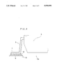
- FIG. 4 is a partially fragmented sectional view for illustrating a method of mounting such a package on the package substrate 8.
- solder 10 is previously applied to a mounting pad 9 of each electrode portion formed on the surface of the package substrate 8, as shown in FIG. 4.
- a package 6a is so mounted on the package substrate 8 as to bring a soldering portion 7 into prescribed positional relation to the mounting pad 9.
- the soldering portion 7 is soldered to the mounting pad 9 to be electrically and mechanically connected to the same by the solder 10, thereby to complete mounting.
- a first invention comprises a first semiconductor package having external lead terminals upwardly bent with respect to a package surface thereof; a second semiconductor package having external lead terminals downwardly bent with respect to a package surface thereof; a package substrate mounted on one surface with the first and second semiconductor packages through the external lead terminals respectively; and connecting means for electrically connecting the external lead terminals of the first semiconductor package with corresponding ones of the external lead terminals of the second semiconductor package.
- a second invention comprises a first semiconductor package having external lead terminals upwardly bent with respect to a package surface thereof; a second semiconductor package having external lead terminals downwardly bent with respect to a package surface thereof, a package substrate mounted on a first surface with the first semiconductor package through the external lead terminals thereof as well as mounted on a second surface with the second semiconductor package through the external lead terminals thereof in correspondence to the first semiconductor package; and connecting means for electrically connecting the external lead terminals of the first semiconductor package with corresponding ones of the external lead terminals of the second semiconductor package.
- a principal object of the present invention is to provide a semiconductor device which can electrically connect external lead terminals of the same pin numbers by simply drawing around wires in single-surface mounting of semiconductor packages.
- Another object of the present invention is to provide a semiconductor device which can electrically connect external lead terminals of the same pin numbers only by through holes in double-surface mounting of semiconductor packages.
- FIG. 1A is a plan view showing an A-type package
- FIG. 1B is a side elevational view showing the A-type package
- FIG. 1C is a front elevational view showing the A-type package
- FIG. 1D is a sectional view showing the A-type package
- FIG. 2 illustrates a conventional semiconductor device having a package substrate which is mounted on both surfaces with a pair of A-type packages as shown in FIG. 1;
- FIG. 3 illustrates a conventional semiconductor device having a package substrate which is mounted on its one surface with a pair of A-type packages as shown in FIG. 1;
- FIG. 4 is a partially fragmented sectional view for illustrating a method of mounting a package on a package substrate
- FIG. 5A is a plan view showing a package having upwardly bent external lead terminals (hereinafter referred to as a B-type package);
- FIG. 5B is a side elevational view showing the B-type package
- FIG. 5D is a sectional view showing the B-type package
- FIG. 6 illustrates a semiconductor device according to an embodiment of a first invention
- FIG. 6 illustrates a semiconductor device according to an embodiment of a first invention.
- numerals identical to those of FIG. 2 indicate the same components.
- An A-type package 6a as shown in FIGS. 1A to 1D is mounted on a first surface of a package substrate 8.
- a B-type package 6b as shown in FIGS. 5A to 5D is mounted on a second surface of the package substrate 8 in correspondence to the A-type package 6a mounted on the first surface of a package substrate 8.
- FIG. 7 illustrates a semiconductor device having a package substrate 8 which is mounted on its one surface with an A-type package 6a as shown in FIGS. 1A to 1D and a B-type package 6b as shown in FIGS. 5A to 5D. As shown in FIG. 7, the A-type package 6a and the B-type package 6b are mounted on one surface of the package substrate 8 substantially in parallel to each other.
- the packages are mounted on the package substrate 8 in a similar manner to the conventional one, and hence redundant description is omitted.
- the external lead terminals 3 of the packages 6a and 6b having the same pin numbers are opposite to each other.
- a pin p 1 of the package 6a mounted on the first surface of the package substrate 8 corresponds to an external lead terminal 3, indicated as a pin p 1 , of the package 6b mounted on the second surface of the package substrate 8.
- the external lead terminals 3 having the same pin numbers can be electrically connected with each other by simply forming through holes 11 in positions of the package substrate 8 corresponding to the external lead terminals 3 to be connected and filling up the through holes 11 by conductive materials.
- external lead terminals 3 of the package 6a are located in positions linearly symmetrical to external lead terminals 3 of the package 6b having the same pin numbers.
- the external lead terminals 3 of the same pin numbers in the packages 6a and 6b can be electrically connected with each other simply by drawing around wires 12, with no intersection of the wires 12 or no provision of through holes or jumper wires.
Abstract
Two types of semiconductor packages (6a, 6b), being different in direction of bending of external lead terminals (3) from each other, are prepared to be mounted on a single surface or both surfaces of a package substrate. In case of single-surface mounting, the external lead terminals (3) of the same pin numbers can be electrically connected with each other by drawing around wires (9). In case of double-surface mounting, the external lead terminals (3) of the same pin numbers can be electrically connected with each other by through holes.
Description
1. Field of the Invention
The present invention relates to a semiconductor device which is formed by mounting semiconductor packages having integrated circuits on a package substrate.
2. DESCRIPTION OF THE PRIOR ART
FIG. 1A is a plan view showing a small outline package having external lead terminals downwardly bent with respect to a package surface thereof (hereinafter referred to as an A-type package) and FIG. 1B is a side elevational view of the A-type package, while FIG. 1C is a front elevational view of the A-type package and FIG. 1D is a sectional view thereof. As shown in FIG. 1D, a semiconductor chip 2 is placed on a die pad 1. A bonding pad (not shown) provided on the semiconductor chip 2 is electrically connected with external lead terminals 3 by bonding wires 4. The die pad 1, the semiconductor chip 2, parts of the external lead terminals 3 and the bonding wires 4 are packaged by mold resin 5, to form a small outline package 6a whose appearance is as shown in FIGS. 1A to 1C. This package 6a is characterized in that the external lead terminals 3 are downwardly bent at an angle of about 90° with respect to a package surface thereof as shown in FIGS. 1B to 1D, while forward end portions of the external lead terminals 3 are further bent at an angle of about 90° to outwardly extend from the package 6a.
Such forward end portions of the external lead terminals 3 serve as soldering portions 7 to be soldered to a package substrate as hereinafter described. Referring to FIG. 1A, the lower leftmost external lead terminal 3 is referred to as a pin p1 and the lower rightmost external lead terminal 3 is referred to as a pin p14, while the upper rightmost external lead terminal 3 is referred to as a pin p15 and the upper leftmost external lead terminal 3 is referred to as a pin p28, for convenience of the following description.
FIG. 2 illustrates a semiconductor device having a package substrate 8 which is provided on both surfaces with a pair of A-type packages 6a as shown in FIGS. 1A to 1D. One of the A-type packages 6a is mounted on a first surface of the package substrate 8. The other A-type package 6a is mounted on a second surface of the package substrate 8 in correspondence to the package 6a mounted on the first surface.
FIG. 3 illustrates a semiconductor device having a package substrate 8 which is provided on its one surface with a plurality of A-type packages 6a as shown in FIGS. 1A to 1D. As shown in FIG. 3, such A-type packages 6a are mounted to be substantially parallel to each other.
FIG. 4 is a partially fragmented sectional view for illustrating a method of mounting such a package on the package substrate 8. First, solder 10 is previously applied to a mounting pad 9 of each electrode portion formed on the surface of the package substrate 8, as shown in FIG. 4. Then a package 6a is so mounted on the package substrate 8 as to bring a soldering portion 7 into prescribed positional relation to the mounting pad 9. Thereafter the soldering portion 7 is soldered to the mounting pad 9 to be electrically and mechanically connected to the same by the solder 10, thereby to complete mounting.
Consider such case where a pair of packages 6a are mounted on both surfaces of the package substrate 8 as shown in FIG. 2, so that external lead terminals 3 of the packages 6a having the same pin numbers are connected with each other. In this case, it is impossible to connect the external lead terminals 3 having the same pin numbers by merely connecting the external lead terminals 3 of the pair of packages 6a through holes provided on the package substrate 8. This is because the external lead terminals 3 having the same pin numbers are not rendered opposite to each other in the structure as shown in FIG. 2. For example, the pin p1 within the external lead terminals 3 of the package 6a mounted on the first surface of the package substrate 8 is rendered opposite to the pin p14 or p28 within the external lead terminals 3 of the package 6a provided on the second surface of the package substrate 8.
Further, consider such case where the three or more pairs of external lead terminals 3 having the same pin numbers are connected with each other within those of a pair of packages 6a provided on one surface of the package substrate 8. In this case, it is impossible to connect the external lead terminals 3 of the packages 6a having the same pin umbers with each other by simply drawing around wires 12 on the surface carrying the packages 6a. This is because the wires 12 inevitably intersect with each other in any position to cause a short. When pins p1, p14, p15 and p28 of the two packages 6a are connected with each other as shown in FIG. 3, for example, the wires 12 inevitably intersect with each other in two positions. Therefore, jumper wires and through holes 13 as shown in FIG. 3 must be provided in such positions, in order to prevent shorting by avoiding such intersection of the wires 12.
A first invention comprises a first semiconductor package having external lead terminals upwardly bent with respect to a package surface thereof; a second semiconductor package having external lead terminals downwardly bent with respect to a package surface thereof; a package substrate mounted on one surface with the first and second semiconductor packages through the external lead terminals respectively; and connecting means for electrically connecting the external lead terminals of the first semiconductor package with corresponding ones of the external lead terminals of the second semiconductor package.
A second invention comprises a first semiconductor package having external lead terminals upwardly bent with respect to a package surface thereof; a second semiconductor package having external lead terminals downwardly bent with respect to a package surface thereof, a package substrate mounted on a first surface with the first semiconductor package through the external lead terminals thereof as well as mounted on a second surface with the second semiconductor package through the external lead terminals thereof in correspondence to the first semiconductor package; and connecting means for electrically connecting the external lead terminals of the first semiconductor package with corresponding ones of the external lead terminals of the second semiconductor package.
Accordingly, a principal object of the present invention is to provide a semiconductor device which can electrically connect external lead terminals of the same pin numbers by simply drawing around wires in single-surface mounting of semiconductor packages.
Another object of the present invention is to provide a semiconductor device which can electrically connect external lead terminals of the same pin numbers only by through holes in double-surface mounting of semiconductor packages.
These and other objects, features, aspects and advantages of the present invention will become more apparent from the following detailed description of the present invention when taken in conjunction with the accompanying drawings.
FIG. 1A is a plan view showing an A-type package;
FIG. 1B is a side elevational view showing the A-type package;
FIG. 1C is a front elevational view showing the A-type package;
FIG. 1D is a sectional view showing the A-type package;
FIG. 2 illustrates a conventional semiconductor device having a package substrate which is mounted on both surfaces with a pair of A-type packages as shown in FIG. 1;
FIG. 3 illustrates a conventional semiconductor device having a package substrate which is mounted on its one surface with a pair of A-type packages as shown in FIG. 1;
FIG. 4 is a partially fragmented sectional view for illustrating a method of mounting a package on a package substrate;
FIG. 5A is a plan view showing a package having upwardly bent external lead terminals (hereinafter referred to as a B-type package);
FIG. 5B is a side elevational view showing the B-type package;
FIG. 5C is a front elevational view showing the B-type package;
FIG. 5D is a sectional view showing the B-type package;
FIG. 6 illustrates a semiconductor device according to an embodiment of a first invention; and
FIG. 7 illustrates a semiconductor device according to an embodiment of a second invention.
FIG. 5A is a plan view showing a B-type small outline package and FIG. 5B is a side elevational view thereof, while FIG. 5C is a front elevational view thereof and FIG. 5D is a sectional view thereof. The B-type package is different from the aforementioned A-type package in that external lead terminals 3 are upwardly bent at an angle of about 90° with respect to a package surface thereof as shown in FIG. 5D, dissimilarly to those of the A-type package as shown in FIG. 1D. The B-type package is absolutely identical in other structure to the A-type package.
FIG. 6 illustrates a semiconductor device according to an embodiment of a first invention. Referring to FIG. 6, numerals identical to those of FIG. 2 indicate the same components. An A-type package 6a as shown in FIGS. 1A to 1D is mounted on a first surface of a package substrate 8. A B-type package 6b as shown in FIGS. 5A to 5D is mounted on a second surface of the package substrate 8 in correspondence to the A-type package 6a mounted on the first surface of a package substrate 8.
FIG. 7 illustrates a semiconductor device having a package substrate 8 which is mounted on its one surface with an A-type package 6a as shown in FIGS. 1A to 1D and a B-type package 6b as shown in FIGS. 5A to 5D. As shown in FIG. 7, the A-type package 6a and the B-type package 6b are mounted on one surface of the package substrate 8 substantially in parallel to each other.
The packages are mounted on the package substrate 8 in a similar manner to the conventional one, and hence redundant description is omitted.
Consider such case where, within external lead terminals 3 of the packages 6a and 6b mounted on the package substrate 8, those having the same pin numbers are connected to each other.
In the case of double-surface mounting as shown in FIG. 6, the external lead terminals 3 of the packages 6a and 6b having the same pin numbers are opposite to each other. For example, a pin p1 of the package 6a mounted on the first surface of the package substrate 8 corresponds to an external lead terminal 3, indicated as a pin p1, of the package 6b mounted on the second surface of the package substrate 8. Thus, the external lead terminals 3 having the same pin numbers can be electrically connected with each other by simply forming through holes 11 in positions of the package substrate 8 corresponding to the external lead terminals 3 to be connected and filling up the through holes 11 by conductive materials.
In the case of single-surface mounting as shown in FIG. 7, external lead terminals 3 of the package 6a are located in positions linearly symmetrical to external lead terminals 3 of the package 6b having the same pin numbers. Thus, the external lead terminals 3 of the same pin numbers in the packages 6a and 6b can be electrically connected with each other simply by drawing around wires 12, with no intersection of the wires 12 or no provision of through holes or jumper wires.
While small outline packages 6a and 6b are described above, the present invention can also be applied to a plastic leaded chip carrier or a small outline package with J lead. In other words, the present invention is applicable to all types of surface-mounting type packages.
Although the present invention has been described and illustrated in detail, it is clearly understood that the same is by way of illustration and example only and is not to be taken by way of limitation, the spirit and scope of the present invention being limited only by the terms of the appended claims.
Claims (5)
1. A semiconductor device comprising
a first semiconductor package having external lead terminals arranged according to a predetermined configuration and upwardly bent with respect to a package surface thereof;
a second semiconductor package having external lead terminals arranged according to the same predetermined configuration as said first semiconductor package and downwardly bent with respect to a package surface thereof;
a package substrate having said first semiconductor package thereof mounted on one surface whereby the upward surface of said first package faces a first surface of said package substrate and having mounted on the first surface of said package substrate said second semiconductor package such that the downward surface of said second package faces said first surface of said package substrate; and
connecting means for electrically connecting said external lead terminals of said first semiconductor package with corresponding ones of said external lead terminals of said second semiconductor package.
2. A semiconductor device in accordance with claim 1, wherein
said first and second semiconductor packages are mounted substantially in a parallel manner to each other.
3. A semiconductor device in accordance with claim 1, wherein
said connecting means is formed by wires provided on said one surface of said package substrate.
4. A semiconductor device comprising:
a first semiconductor package having external lead terminals arranged in a predetermined configuration and upwardly bent with respect to a first package surface thereof;
a second semiconductor package having external lead terminals arranged in the same predetermined configuration as said first semiconductor package and downwardly bent with respect to a first package surface thereof;
a package substrate having mounted on a first surface said first semiconductor package such that said first package surface of said first semiconductor package is facing said first surface of said substrate and said second semiconductor package mounted on a second surface of said package substrate such that said first package surface of said second semiconductor package faces said second surface of said package substrate; and
connecting means for electrically connecting said external lead terminals of said first semiconductor package with corresponding ones of said external lead terminals of said second semiconductor package.
5. A semiconductor device in accordance with claim 4, wherein
said connecting means is formed by filling up conductive materials into through holes which is provided in said package substrate to pass through regions held by said external lead terminals of said first semiconductor package and said corresponding ones of said external lead terminals of said second semiconductor package.
Applications Claiming Priority (2)
| Application Number | Priority Date | Filing Date | Title |
|---|---|---|---|
| JP62130683A JPS63296292A (en) | 1987-05-27 | 1987-05-27 | Semiconductor device |
| JP62-130683 | 1987-05-27 |
Publications (1)
| Publication Number | Publication Date |
|---|---|
| US4994896A true US4994896A (en) | 1991-02-19 |
Family
ID=15040118
Family Applications (1)
| Application Number | Title | Priority Date | Filing Date |
|---|---|---|---|
| US07/194,944 Expired - Lifetime US4994896A (en) | 1987-05-27 | 1988-05-17 | Semiconductor device |
Country Status (2)
| Country | Link |
|---|---|
| US (1) | US4994896A (en) |
| JP (1) | JPS63296292A (en) |
Cited By (17)
| Publication number | Priority date | Publication date | Assignee | Title |
|---|---|---|---|---|
| EP0484062A1 (en) * | 1990-10-30 | 1992-05-06 | Mitsubishi Denki Kabushiki Kaisha | A semiconductor device comprising two integrated circuit packages |
| EP0538003A1 (en) * | 1991-10-15 | 1993-04-21 | Mitsubishi Denki Kabushiki Kaisha | Method of manufacturing inversion type ICs and IC module using same |
| US5227664A (en) * | 1988-02-26 | 1993-07-13 | Hitachi, Ltd. | Semiconductor device having particular mounting arrangement |
| US5313416A (en) * | 1991-07-03 | 1994-05-17 | Mitsubishi Denki Kabushiki Kaisha | Semiconductor memory control device and method of mounting same in high density |
| US5349233A (en) * | 1992-04-20 | 1994-09-20 | Kabushiki Kaisha Toshiba | Lead frame and semiconductor module using the same having first and second islands and three distinct pluralities of leads and semiconductor module using the lead frame |
| US5408129A (en) * | 1990-04-18 | 1995-04-18 | Rambus, Inc. | Integrated circuit I/O using a high performance bus interface |
| US5420756A (en) * | 1992-06-19 | 1995-05-30 | Kabushiki Kaisha Toshiba | Memory card including stacked semiconductor memory elements located on a printed circuit board having a straight wiring pattern |
| GB2288066A (en) * | 1994-03-31 | 1995-10-04 | Hewlett Packard Co | Integrated circuit having mirror-image pin assignments |
| EP0682366A2 (en) * | 1994-05-12 | 1995-11-15 | Texas Instruments Incorporated | Mounting of integrated circuit devices |
| US5805520A (en) * | 1997-04-25 | 1998-09-08 | Hewlett-Packard Company | Integrated circuit address reconfigurability |
| US5973951A (en) * | 1992-05-19 | 1999-10-26 | Sun Microsystems, Inc. | Single in-line memory module |
| US20050281012A1 (en) * | 2004-06-16 | 2005-12-22 | Charles Clark | Mirror image electrical packages and system for using same |
| US20090051020A1 (en) * | 2007-02-22 | 2009-02-26 | Kabushiki Kaisha Toshiba | Method of manufacturing semiconductor device, and semiconductor device |
| US20090250255A1 (en) * | 2008-04-02 | 2009-10-08 | Spansion Llc | Connections for electronic devices on double-sided circuit board |
| US20130020695A1 (en) * | 2011-07-20 | 2013-01-24 | Hanjoo Na | "L" Shaped Lead Integrated Circuit Package |
| US8569913B2 (en) | 2011-05-16 | 2013-10-29 | Unigen Corporation | Switchable capacitor arrays for preventing power interruptions and extending backup power life |
| CN103515346A (en) * | 2012-06-14 | 2014-01-15 | 英飞凌科技股份有限公司 | Semiconductor module and method of formation thereof |
Citations (6)
| Publication number | Priority date | Publication date | Assignee | Title |
|---|---|---|---|---|
| JPS54140468A (en) * | 1978-04-24 | 1979-10-31 | Hitachi Ltd | Glass sealing package type device and its manufacture |
| JPS58159360A (en) * | 1982-03-17 | 1983-09-21 | Fujitsu Ltd | Semiconductor device |
| US4482781A (en) * | 1982-05-17 | 1984-11-13 | National Semiconductor Corporation | Stabilization of semiconductor device package leads |
| JPS60220955A (en) * | 1984-04-17 | 1985-11-05 | Toshiba Corp | Flat package tupe semiconductor device |
| US4651192A (en) * | 1981-12-04 | 1987-03-17 | Hitachi, Ltd. | Ceramic packaged semiconductor device |
| US4771366A (en) * | 1987-07-06 | 1988-09-13 | International Business Machines Corporation | Ceramic card assembly having enhanced power distribution and cooling |
Family Cites Families (3)
| Publication number | Priority date | Publication date | Assignee | Title |
|---|---|---|---|---|
| JPS6012788A (en) * | 1983-07-01 | 1985-01-23 | 日本電気オフィスシステム株式会社 | Electronic circuit device |
| JPS6046581A (en) * | 1983-08-24 | 1985-03-13 | シャープ株式会社 | Package of device |
| JPS6193694A (en) * | 1984-10-15 | 1986-05-12 | 松下電器産業株式会社 | Ic device |
-
1987
- 1987-05-27 JP JP62130683A patent/JPS63296292A/en active Pending
-
1988
- 1988-05-17 US US07/194,944 patent/US4994896A/en not_active Expired - Lifetime
Patent Citations (7)
| Publication number | Priority date | Publication date | Assignee | Title |
|---|---|---|---|---|
| JPS54140468A (en) * | 1978-04-24 | 1979-10-31 | Hitachi Ltd | Glass sealing package type device and its manufacture |
| US4651192A (en) * | 1981-12-04 | 1987-03-17 | Hitachi, Ltd. | Ceramic packaged semiconductor device |
| JPS58159360A (en) * | 1982-03-17 | 1983-09-21 | Fujitsu Ltd | Semiconductor device |
| US4682207A (en) * | 1982-03-17 | 1987-07-21 | Fujitsu Limited | Semiconductor device including leadless packages and a base plate for mounting the leadless packages |
| US4482781A (en) * | 1982-05-17 | 1984-11-13 | National Semiconductor Corporation | Stabilization of semiconductor device package leads |
| JPS60220955A (en) * | 1984-04-17 | 1985-11-05 | Toshiba Corp | Flat package tupe semiconductor device |
| US4771366A (en) * | 1987-07-06 | 1988-09-13 | International Business Machines Corporation | Ceramic card assembly having enhanced power distribution and cooling |
Non-Patent Citations (2)
| Title |
|---|
| Iafrate, "High Density and Speed Performance Chip Joining Procedure and Package", IBM Tech. Disclosure Bulletin, vol. 15, No. 4, 9/72, p. 1281. |
| Iafrate, High Density and Speed Performance Chip Joining Procedure and Package , IBM Tech. Disclosure Bulletin, vol. 15, No. 4, 9/72, p. 1281. * |
Cited By (30)
| Publication number | Priority date | Publication date | Assignee | Title |
|---|---|---|---|---|
| US5227664A (en) * | 1988-02-26 | 1993-07-13 | Hitachi, Ltd. | Semiconductor device having particular mounting arrangement |
| US5396102A (en) * | 1988-02-26 | 1995-03-07 | Hitachi, Ltd. | Semiconductor device |
| US5408129A (en) * | 1990-04-18 | 1995-04-18 | Rambus, Inc. | Integrated circuit I/O using a high performance bus interface |
| EP0484062A1 (en) * | 1990-10-30 | 1992-05-06 | Mitsubishi Denki Kabushiki Kaisha | A semiconductor device comprising two integrated circuit packages |
| US5309020A (en) * | 1990-10-30 | 1994-05-03 | Mitsubishi Denki Kabushiki Kaisha | Packaged semiconductor device assembly including two interconnected packaged semiconductor devices mounted on a common substrate |
| US5313416A (en) * | 1991-07-03 | 1994-05-17 | Mitsubishi Denki Kabushiki Kaisha | Semiconductor memory control device and method of mounting same in high density |
| EP0538003A1 (en) * | 1991-10-15 | 1993-04-21 | Mitsubishi Denki Kabushiki Kaisha | Method of manufacturing inversion type ICs and IC module using same |
| US5303120A (en) * | 1991-10-15 | 1994-04-12 | Mitsubishi Denki Kabushiki Kaisha | Method of manufacturing inversion type IC's and IC module using same |
| USRE36077E (en) * | 1991-10-15 | 1999-02-02 | Mitsubishi Denki Kabushiki Kaisha | Method of manufacturing inversion type IC's and IC module using same |
| US5349233A (en) * | 1992-04-20 | 1994-09-20 | Kabushiki Kaisha Toshiba | Lead frame and semiconductor module using the same having first and second islands and three distinct pluralities of leads and semiconductor module using the lead frame |
| US5973951A (en) * | 1992-05-19 | 1999-10-26 | Sun Microsystems, Inc. | Single in-line memory module |
| US5420756A (en) * | 1992-06-19 | 1995-05-30 | Kabushiki Kaisha Toshiba | Memory card including stacked semiconductor memory elements located on a printed circuit board having a straight wiring pattern |
| US5502621A (en) * | 1994-03-31 | 1996-03-26 | Hewlett-Packard Company | Mirrored pin assignment for two sided multi-chip layout |
| DE19511249A1 (en) * | 1994-03-31 | 1995-10-05 | Hewlett Packard Co | Mirrored pin assignment for a two-sided multichip arrangement |
| GB2288066A (en) * | 1994-03-31 | 1995-10-04 | Hewlett Packard Co | Integrated circuit having mirror-image pin assignments |
| EP0682366A3 (en) * | 1994-05-12 | 1996-03-06 | Texas Instruments Inc | Mounting of integrated circuit devices. |
| EP0682366A2 (en) * | 1994-05-12 | 1995-11-15 | Texas Instruments Incorporated | Mounting of integrated circuit devices |
| US5671125A (en) * | 1994-05-12 | 1997-09-23 | Texas Instruments Incorporated | Vertical package mounted on both sides of a printed circuit board |
| EP0997944A2 (en) * | 1994-05-12 | 2000-05-03 | Texas Instruments Incorporated | Printed circuit board with integrated circuit devices mounted on both sides thereof |
| EP0997944A3 (en) * | 1994-05-12 | 2000-05-10 | Texas Instruments Incorporated | Printed circuit board with integrated circuit devices mounted on both sides thereof |
| US5805520A (en) * | 1997-04-25 | 1998-09-08 | Hewlett-Packard Company | Integrated circuit address reconfigurability |
| US20050281012A1 (en) * | 2004-06-16 | 2005-12-22 | Charles Clark | Mirror image electrical packages and system for using same |
| US7289332B2 (en) * | 2004-06-16 | 2007-10-30 | Liberty University | Mirror image electrical packages and system for using same |
| US20090051020A1 (en) * | 2007-02-22 | 2009-02-26 | Kabushiki Kaisha Toshiba | Method of manufacturing semiconductor device, and semiconductor device |
| US20090250255A1 (en) * | 2008-04-02 | 2009-10-08 | Spansion Llc | Connections for electronic devices on double-sided circuit board |
| US8228679B2 (en) * | 2008-04-02 | 2012-07-24 | Spansion Llc | Connections for electronic devices on double-sided circuit board |
| US8569913B2 (en) | 2011-05-16 | 2013-10-29 | Unigen Corporation | Switchable capacitor arrays for preventing power interruptions and extending backup power life |
| US20130020695A1 (en) * | 2011-07-20 | 2013-01-24 | Hanjoo Na | "L" Shaped Lead Integrated Circuit Package |
| US9601417B2 (en) * | 2011-07-20 | 2017-03-21 | Unigen Corporation | “L” shaped lead integrated circuit package |
| CN103515346A (en) * | 2012-06-14 | 2014-01-15 | 英飞凌科技股份有限公司 | Semiconductor module and method of formation thereof |
Also Published As
| Publication number | Publication date |
|---|---|
| JPS63296292A (en) | 1988-12-02 |
Similar Documents
| Publication | Publication Date | Title |
|---|---|---|
| US4994896A (en) | Semiconductor device | |
| US4677526A (en) | Plastic pin grid array chip carrier | |
| US5413970A (en) | Process for manufacturing a semiconductor package having two rows of interdigitated leads | |
| US5731631A (en) | Semiconductor device with tape automated bonding element | |
| US6570249B1 (en) | Semiconductor package | |
| US5777382A (en) | Plastic packaging for a surface mounted integrated circuit | |
| US6627981B2 (en) | Resin-packaged semiconductor device | |
| US4616406A (en) | Process of making a semiconductor device having parallel leads directly connected perpendicular to integrated circuit layers therein | |
| US5942795A (en) | Leaded substrate carrier for integrated circuit device and leaded substrate carrier device assembly | |
| US5444304A (en) | Semiconductor device having a radiating part | |
| US4951124A (en) | Semiconductor device | |
| JPH07202378A (en) | Packaged electron hardware unit | |
| US6130478A (en) | Polymer stud grid array for microwave circuit arrangements | |
| US5309020A (en) | Packaged semiconductor device assembly including two interconnected packaged semiconductor devices mounted on a common substrate | |
| US5712570A (en) | Method for checking a wire bond of a semiconductor package | |
| US5107329A (en) | Pin-grid array semiconductor device | |
| KR100226335B1 (en) | Molded plastic packaging of electronic devices | |
| EP0221496A2 (en) | Integrated circuit package | |
| US5849609A (en) | Semiconductor package and a method of manufacturing thereof | |
| JP3174238B2 (en) | Semiconductor device and method of manufacturing the same | |
| JPH09129796A (en) | Semiconductor device | |
| US6297542B1 (en) | Connecting a die in an integrated circuit module | |
| KR20020003512A (en) | Semiconductor device and method of manufacturing the same | |
| KR930011117B1 (en) | Mounting method of semiconductor package | |
| JPH04216653A (en) | Package for semiconductor integrated circuit and its packaging method |
Legal Events
| Date | Code | Title | Description |
|---|---|---|---|
| AS | Assignment |
Owner name: MITSUBISHI DENKI KABUSHIKI KAISHA, JAPAN Free format text: ASSIGNMENT OF ASSIGNORS INTEREST.;ASSIGNORS:UEMURA, SHUNICHI;MURASAWA, YASUHIRO;REEL/FRAME:005483/0893 Effective date: 19880427 |
|
| STCF | Information on status: patent grant |
Free format text: PATENTED CASE |
|
| FEPP | Fee payment procedure |
Free format text: PAYOR NUMBER ASSIGNED (ORIGINAL EVENT CODE: ASPN); ENTITY STATUS OF PATENT OWNER: LARGE ENTITY |
|
| CC | Certificate of correction | ||
| FPAY | Fee payment |
Year of fee payment: 4 |
|
| FPAY | Fee payment |
Year of fee payment: 8 |
|
| FPAY | Fee payment |
Year of fee payment: 12 |