US4901344A - Telephone system digital channel bank interface - Google Patents
Telephone system digital channel bank interface Download PDFInfo
- Publication number
- US4901344A US4901344A US07/238,617 US23861788A US4901344A US 4901344 A US4901344 A US 4901344A US 23861788 A US23861788 A US 23861788A US 4901344 A US4901344 A US 4901344A
- Authority
- US
- United States
- Prior art keywords
- ask
- telephone
- electronic business
- signals
- central office
- Prior art date
- Legal status (The legal status is an assumption and is not a legal conclusion. Google has not performed a legal analysis and makes no representation as to the accuracy of the status listed.)
- Expired - Lifetime
Links
Images
Classifications
-
- H—ELECTRICITY
- H04—ELECTRIC COMMUNICATION TECHNIQUE
- H04M—TELEPHONIC COMMUNICATION
- H04M9/00—Arrangements for interconnection not involving centralised switching
- H04M9/002—Arrangements for interconnection not involving centralised switching with subscriber controlled access to a line, i.e. key telephone systems
- H04M9/003—Transmission of control signals from or to the key telephone set; signalling equipment at key telephone set, e.g. keyboard or display equipment
-
- H—ELECTRICITY
- H04—ELECTRIC COMMUNICATION TECHNIQUE
- H04J—MULTIPLEX COMMUNICATION
- H04J3/00—Time-division multiplex systems
- H04J3/02—Details
- H04J3/12—Arrangements providing for calling or supervisory signals
- H04J3/125—One of the channel pulses or the synchronisation pulse is also used for transmitting monitoring or supervisory signals
-
- H—ELECTRICITY
- H04—ELECTRIC COMMUNICATION TECHNIQUE
- H04L—TRANSMISSION OF DIGITAL INFORMATION, e.g. TELEGRAPHIC COMMUNICATION
- H04L25/00—Baseband systems
- H04L25/38—Synchronous or start-stop systems, e.g. for Baudot code
- H04L25/40—Transmitting circuits; Receiving circuits
- H04L25/49—Transmitting circuits; Receiving circuits using code conversion at the transmitter; using predistortion; using insertion of idle bits for obtaining a desired frequency spectrum; using three or more amplitude levels ; Baseband coding techniques specific to data transmission systems
- H04L25/4917—Transmitting circuits; Receiving circuits using code conversion at the transmitter; using predistortion; using insertion of idle bits for obtaining a desired frequency spectrum; using three or more amplitude levels ; Baseband coding techniques specific to data transmission systems using multilevel codes
- H04L25/4927—Transmitting circuits; Receiving circuits using code conversion at the transmitter; using predistortion; using insertion of idle bits for obtaining a desired frequency spectrum; using three or more amplitude levels ; Baseband coding techniques specific to data transmission systems using multilevel codes using levels matched to the quantisation levels of the channel
-
- H—ELECTRICITY
- H04—ELECTRIC COMMUNICATION TECHNIQUE
- H04M—TELEPHONIC COMMUNICATION
- H04M11/00—Telephonic communication systems specially adapted for combination with other electrical systems
- H04M11/06—Simultaneous speech and data transmission, e.g. telegraphic transmission over the same conductors
- H04M11/068—Simultaneous speech and data transmission, e.g. telegraphic transmission over the same conductors using time division multiplex techniques
-
- H—ELECTRICITY
- H04—ELECTRIC COMMUNICATION TECHNIQUE
- H04M—TELEPHONIC COMMUNICATION
- H04M3/00—Automatic or semi-automatic exchanges
- H04M3/42—Systems providing special services or facilities to subscribers
- H04M3/42314—Systems providing special services or facilities to subscribers in private branch exchanges
Definitions
- This invention relates to a Primary Multiplex Terminal (DS-1) Channel Unit Interface permitting simultaneous Voice and Out-of-Band Signaling (8 kHz ASK Messages) transmission over one Voice Channel for Centrex III service using an Electronic Business Set (EBS).
- DS-1 Primary Multiplex Terminal
- EBS Electronic Business Set
- the strategy of furnishing business communications service depends on the size of the customer organization, the manner in which it is dispersed over different locations, and the number of people at each location. In addition, the manner in which the needs are fulfilled depends on the service features to be provided in addition to the basic features of intercommunication.
- PBX private branch exchange
- PABX private branch exchange
- the centrex system has several advantages including lower cost, better maintenance because of the location of the equipment at the local telephone company office, and also has battery backup which was normally not available with PABX, thereby preserving operability of the telephone system during power failures. Additionally, the digital centrex system such as that provided on a Northern Telecom DMS-100 digital switch could be upgraded automatically simply by replacing the software package with minimum disturbance of the customer's service.
- EBS Electronic Business Set
- the EBS is a multi-line, fully-featured business communication set equipped with a 32-character alphanumeric liquid crystal display that operates over a single pair of wires regardless of the number of assigned directory numbers.
- These sets contain programmable special function buttons and code generating hardware. At the touch of a single button, special functions can be performed such as hold, interconnecting parties for a conference call, call transfer and the like.
- Regular telephone sets could be used with the system, but it would then be necessary for the user to key in a sequence of special codes for each function using the twelve-key pad.
- the Electronic Business Set instruments have the functions of feature keys, signalling and supervision which are accomplished with binary codes using above-voiceband signals amplitude-shift-keyed at 8 kHz.
- the above-voiceband signal is a low-level, 8 kHz amplitude-shift-keyed (ASK) 1000 baud message containing 16 bits, using half-duplex transmission.
- ASK amplitude-shift-keyed
- the presence of the 8 kHz carrier indicates a binary "1" and the absence of the 8 kHz carrier is interpreted as a binary "0”.
- Supervision off-hook/on-hook
- feature activation i.e., hold, conference call
- signaling dialing
- the 8 kHz control signals are transmitted over telephone lines, and because of the attenuation characteristics at 8 kHz of the conventional non-loaded pairs of wires which are primarily intended to carry voice frequency (VF) signals, the subscriber loops are limited to 15,000 ft. using 26 AWG wire. Thus, only those customers within a 15,000 ft. radius of the Centrex III Central Office (DMS-100) can be served. While a system such as this is workable in some customer environments, a customer having multiple locations distributed several kilometers from each other could not employ this system and are therefore denied this desirable service.
- DMS-100 Centrex III Central Office
- a Digital Loop Carrier System currently in use in various telephone environments known as the Subscriber Loop Carrier System (i.e., SLC-96), is a digital subscriber carrier system which provides for up to 96 subscriber channels between a central office terminal (COT) and a remote terminal (RT) using up to 4 digital lines (Tl) or other digital transmission facilities (e.g., fiber optics).
- COT central office terminal
- RT remote terminal
- Tl digital lines
- fiber optics e.g., fiber optics
- an object of the present invention is to provide a technique for including the ASK 8 kHz messages within the normal VF bandwidth (about 300 to about 3400 Hz) without affecting transmission parameters.
- the invention must also provide transparency of the channel bank to the central office and the EBS, compatibly with line diagnostics provided by the central office, standard customer loop lengths ( ⁇ 15 kft.) and simplex powering toward the Electronic Business Set.
- the invention comprises a telephone system including a remote terminal with a plurality of electronic business set telephone instruments connected to the remote terminal, each electronic business set telephone instrument including a handset, a hook switch, a dial tone-generating key pad, a plurality of function keys and means responsive to actuation of each function key to generate a unique ASK function code including a sequence of pulses of a tone at a frequency significantly above voiceband frequency.
- a central office including switching means for directing calls to a telephone instrument identified by a dialing sequence, is connected to the remote terminal by a plurality of telephone lines.
- the remote terminal and the central office each includes coder-decoder means which, in one direction, receives a composite signal including voice frequency analog voice signals and the function codes from each electronic business set and produces a sequence of digital output words representative of the analog voice signals for delivery to the telephone lines, each digital word produced by the coder-decoder means including 8 bits of which the least significant bit is set at a first predetermined level when an ASK signal is present and a second predetermined level when no ASK signal is present.
- the coder-decoder converts received digital words into analog signals for delivery to designated ones of the electronic business set telephone instruments, whereby said ASK function code is transmitted from one instrument to another without increasing the bandwidth of the telephone lines.
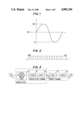
- FIG. 1 is an explanatory waveform diagram illustrating the sampling of an analog voice signal
- FIG. 2 is an illustration of the bit format of a digital word produced by apparatus in accordance with the invention
- FIG. 3 is a simplified schematic block diagram of a part of the apparatus in accordance with the invention.
- FIGS. 4 and 5 are schematic block diagrams of apparatus usable in the Central Office terminal and Remote Terminal, respectively, in accordance with the invention
- FIG. 6 is a schematic block diagram of a bandpass filter usable in the apparatus of FIGS. 4 and 5;
- FIG. 7 is a schematic block diagram of a control data transmit unit usable in the apparatus of FIGS. 4 and 5;
- FIG. 8 is a schematic block diagram of a control data receive unit usable in the apparatus of FIGS. 4 and 5;
- FIG. 8A is a schematic block diagram of a sine wave generator usable in the apparatus of FIG. 4 and 5.
- FIG. 9A-9L are timing diagram showing the states of signals in various parts of the transmit unit.
- FIGS. 10 and 11 are timing diagrams at two different scales showing the states of signals in various parts of the receive unit.
- PCM Pulse Code Modulation
- Bank Digital Loop Carrier System
- the basic components of the PCM channel bank are channel units to interfaceanalog voice frequency (VF) along with above-voice ASK messages which include the technique of the present invention, common equipment to multiplex the channel signals, and interface digital carrier facilities.
- the major functions of the common equipment are framing (frame recognition) and signal formatting.
- Common equipment includes power and alarm modules.
- PCM channel banks are full duplex (two-way operation)terminals.
- PCM channel units in accordance with the invention provide the interface toVF lines (EBS). They perform the function of PAM (Pulse Amplitude Modulation) sampling the VF signals; they also convert the PAM samples to PCM 8 bit octets.
- the companding and codec (coder-decoder) functions transform the PAM samples to 8-bit words (octets).
- the common equipment section of the channel bank comprises the transmit/receive, line interface, special service module, alarm and power units which are common to all channels of the PCM bank.
- the transmit unit interleaves the 8-bit PCM octet with 23 octets from the other channels together with a framing bit to produce a DS-1 frame.
- the frame repetition rate is the channel sampling rate of 8000 Hz. Therefore, line rate becomes:
- the line interface unit converts the unipolar Non-Return to Zero (NRZ) signal format (used internally in the channel bank) to a bipolar AlternateMark Inversion (AMI) format for transmission over digital carrier facilities.
- NRZ Non-Return to Zero
- AMI AlternateMark Inversion
- the line interface unit along with the special service module performs the complementary function of the transmit/receive unit by separating the DS-1signal into its component channels.
- the line interface unit accomplishes this by employing a bipolar AMI to unipolar NRZ conversion and frame recognition, demultiplexing into the individual channels for decoding and,finally, expansion of the decoded signals to original PAM samples.
- the present invention in part, is based upon the recognition of the fact that the feature control codes are only transmitted on the order of 1% or less of the off-hook time. The remainder of the time involves voice transmission with no more codes being sent unless another feature such as hold or conference call is needed.
- the voice wave form As shown in FIG. 1, the voice wave form, sampled at every 125 ⁇ sec. (1/8000 Hz), is pulse amplitude modulated at 256 possible discrete levels,retrieved and reproduced.
- a cycle of this idealized sine wave is shown in FIG. 1 with the 256 possible levels being illustrated along the vertical Yaxis.
- the X axis shows the sampling intervals.
- FIG. 2 is an 8-bit octet having 256 possible values. As represented in FIG. 2, the most significant bit will be depicted as being on the left and the least significant bit (LSB) on the right.
- LSB least significant bit
- the sampling rate of the PCM system results in a sample each 125 microseconds.
- the ASK binary message of the EBS is sent at a frequency of 8 kHz and, in a signal at that frequency, the interval between periods is also 125 ⁇ s. Accordingly, there is approximately a 100% chance that all periods will be detected.
- the least significant bit of the voice signal sample is used in a distinctive fashion to represent the DMS-100 central office/EBS signalling status.
- the system is not asynchronous in the usual sense of that term, but once anASK binary message signal is sent from either the central office or an EBS,the system requires that a "hand shake" acknowledgement must be received by17 milliseconds after the beginning of the ASK transmission or a message retransmission is requested. It is therefore necessary to check for the existence of an ASK signal every 125 ⁇ s.
- the status of the least significant bit is altered to indicate the presence or absence of this message.
- the LSB thus is "borrowed” or monitored in such a way that it always indicates the status of the ASK message without significantly degrading the voice information insofar as the users of the system are concerned.
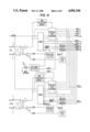
- FIG. 3 A highly simplified schematic of a small part of the telephone system is shown in FIG. 3 in which an EBS instrument is connected to a DMS 12 which responds to off-hook signals from EBS 11 and dial signals to connect the instrument to the desired EBS instrument 22.
- the connection is made with atwo-wire loop coupled through a hybrid circuit 14 in a conventional fashion.
- the output of the hybrid circuit is then connected to the codec 16 which performs the analog to digital conversion for multiplexing purposes to other channels.
- the multiplexed PCM signal composed of 1.544 megabits/second is coupled onto a Tl line 18 which ultimately reaches the remote coder-decoder 20 which shifts the associated 8-bit signal and returns it to analog form for connection through a hybrid circuit 21 to the electronic business set 22.
- units 12, 14 and 16 are part of the COT and units 20 and 21 are part of the RT.
- There are normally 96 hybrid and CODEC units at each end 48 printed circuit cards with two sets per card), each of these units also including other circuitry as
- the remote unit 20 checks to see whether the least significant bit of the octet received indicates the existence ofan ASK message. Depending upon the state of the least significant bit, the internal circuitry of the remote unit will either generate an 8 kHz ASK signal or not. It is important to recognize that the actual carrier frequency of the ASK message could be of any value because the determiningsignal controlling whether the 8 kHz is on or off is a digital state. This is a significant difference from the prior art in which it was considered necessary to have greater bandwidth to transmit the 8 kHz ASK signal. In the present system, the existence or absence thereof is determined by the state of the least significant bit, requiring no additional bandwidth at all.
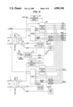
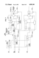
- FIGS. 4 and 5 More complete schematic diagrams are shown in FIGS. 4 and 5 wherein FIG. 4 shows the COT circuit and FIG. 5 the RT circuit, the circuits being very similar to each other.
- FIG. 5 the circuit operation willbe considered under the conditions that an incoming call is being received,i.e., a call from the central office (COT) to an electronic business set atthe remote terminal.
- a ring signal is transmitted from the central office line card to the Tip and Ring terminals of the COT EBS channel unit.
- the ring signal has two frequencies, 513 and 649 Hz and alternates between those two signals at a frequency of 9 Hz at a level of -10 dBm0.
- the ring signal also includes an "alert on" ASK message embedded into the first ring burst at a level of -6 dBm0.
- the composite signal is fed to a 2-to-4-wire hybrid circuit 30 and to the inputs of codec circuit 32 for analog to digital conversion.
- the codec circuit includes an anti-aliasing band pass filter (300 to 3400 Hz), a gain amplifier and an analog to digital converter.
- the composite signal is also fed into a filter 34 whichis a fifth and third order 8 kHz high pass filter for detection and conditioning of ASK messages.
- the voice frequency component is removed by filter 34 which preferably exhibits a 100 dB loss at 1000 Hz.
- ASK signals are amplified by two operational amplifiers having a gain of 16.2 to ensure proper detection.
- the detection threshold is set to -10 dBm.
- the detected sine wave is then converted into a square wave through a Schmitt trigger when the filter output signal reaches the negative reference level, set to -14 dB at 8 kHz.
- the presence of a square wave at filter 34 output indicates the presence of an 8 kHz signal and enables the transmit data control circuit 36 for logic processing.
- Data transmission is enabledwith the presence of a logic high at the TSP (N) and TSQ terminals, the timing control signals of the channel bank. During these conditions, 8 bits of data are shifted out by codec circuit 32 approximately 140 nanoseconds later.
- the presence of 8 kHz codes pulls the output on LSBTX conductor 38 low. This low condition indicates the state of the least significant bit (LSB).
- the data from the codec is then substituted according to the state of LSB at each 125 microsecond interval.
- the modified data are then provided (in PCM format) to the transmit/receive unit in the TDATA bus for transmission over the Tl facility toward the remote terminal (RT).
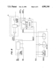
- the remote terminal common equipment receives the DS-1 bit stream, the bipolar PCM 1.544 megabits per second, from the COT, decodes the PCM and forwards the information in NRZ unipolar format to the common bus identified as RNPCM.
- the common equipment addresses the appropriate channel by a logic high on RSP(N) and RSQ, a timing pulse on RWD is then generated by the common equipment to direct the channel unit to accept the PCM sample from the RNPCM bus.
- the incoming 8 bit data is forwarded to the codec 32 and to the ASK control logic circuit 40 for evaluation of the least significant bit.
- the logic state of the extracted LSB is then analyzed by the LSB control circuit.
- a logic low indicates the presence of ASK signal, thus activatingthe 8 kHz sine wave generator 42 until the next LSB change of state from low to high.
- the control feature signal is "reconstructed" at the receiving end without actually transmitting 8 kHz.
- a delay of approximately 312.5 microseconds is required after the receptionof the last logic low of the LSB in order to maintain the output of detection circuit 34 at a level above the detection reference level to prevent potential feedback in the direction opposite to the direction of transmission.
- the analog output signal produced by the 8 kHz oscillator 42 (alert on) message is fed into a summing amplifier 46 which is adjusted to provide a -6 dBm level at 8 kHz.
- the summing amplifier also accepts voice frequency outputs signals (ringing) from the 3900 Hz low pass filter 44. A zero dB insertion loss isprovided prior to transmission through Tip and Ring by the hybrid transformer circuit 30. The composite signal (ringing with the embedded alert on ASK message) is then forwarded to the electronic business set viathe non-loaded cable pair which, as previously indicated, should be less than 15,000 ft. away.
- Channel unit over-voltage protection is achieved by shunt varistors 48 connected across the secondary windings of the hybrid circuits.
- a busy indicator 50 is provided on the faceplate of the unit to monitor thebusy status of the channel unit, both odd and even channels.
- the busy lamp is activated by the off-hook detector 52 which operates with both voice signals, greater than -8 dBm, and ASK 8 kHz messages present on the receive path of transmission.
- a hangover of 2.2 minutes is initiated afterthe detection of the last voice or ASK signal.
- the coder-decoder output is a sequence of serial 8-bit words each 125 ⁇ s in length from the conversion of the voice from analog intodigital form, this output being connected to the control data transmit unit.
- the voice signal is also supplied through a fixed gain,0.dBm amplifier to a special 8 kHz filter which can be described as a high-pass filter and which will be shown in further detail subsequently.
- the output of this filter is an 8 kHz square wave which is subsequently treated as a digital signal, i.e., one which has only two meaningful states.
- the control data transmit unit 36 receives multiplex timing sequence information and puts out a data signal.
- the control circuit removes the least significant bit from the voice word and inserts either a1 or a 0, depending upon whether there is an 8 kHz signal or not.
- the filter output stops for at least 125 microseconds.
- the output is deliveredto an output bus of the channel bank as one of the 24 multiplexed channels.TWD, TSQ and TSPA are timing signals which together produce a window for the data output, thereby defining one of the 24 channels.
- the receive channel must be blocked at the appropriate time or a positive feedback loop would be created. Therefore, after the least significant bit of the output word, a delay of 312.5 ⁇ s is created during which the receiving channel is blocked. This is the SIGCTL signal from the control data receive unit to the control data transmit unit. The duration of the delay is based on filter characteristics.
- a unipolar bit stream after demultiplexing, which includes 7 bits plus the one least significant bit which may or may not be present.
- the control data receiver produces two outputs, one of them being an 8 bit voice frequency and the other being one bit of data.
- the status of the least significant bit is checked. If the least significant bit is detected as indicating a 0, the 8 kHz oscillator in the receiver is activated and the 7 bit string is completed by adding a bit at the end. The least significant bit added is always a 1.If a 1 is already present, it is allowed to remain.
- the 8 bit word is a sign bit which indicates the polarity of the wave represented by that word. If the sign bit is 1, the first half of the analog wave is positive. The 6 subsequent bits are interpreted to the nearest of 128 levels during that positive wave form. If the sign bit is 0, the subsequent bits are evaluated to 128 levels in the negative half of the wave.
- the LSB is always forced high and thereforeinhibits the possibility of sampling even quantifying steps. Thus, there issome theoretical distortion, but it is not discernable to the listener. Themeasurements indicate that the distortion is 0.5 dB higher than if the fullbit stream were used, a level of distortion which is fully acceptable.
- the least significant bit is forced high and when thereis signaling, it is forced low.
- the presence of the least significant bit as a 1 means that all numbers, i.e., all samples, will be odd.
- the 8 kHz oscillator is activated as a function of the state of the LSB andcoupled through the adder to the line. Again, the transmitter is blocked with the same delay as was used in connection with the receiver.
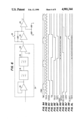
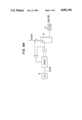
- the ASK detection circuit 34 is shown in more detail in FIG. 6. Essentiallythe same circuit is used on both the central office terminal and receiving terminal except for gain settings as will be noted. The circuit shown is otherwise applicable to both units.
- the input signal including the ASK signal if one is present, is received at the input to a voltage follower circuit 56 which maintains a high impedance at the detection circuit input.
- the output of the voltage follower is delivered to the input of a fifth order Butterworth high pass filter 58 having a transfer function of 100 (log F/F l ), or 30 db/octave.
- the output of filter 58 is fed to a third order Butterworth high pass filter 60 having a transfer function of 60 (log F/F l ), or 18 db/octave.
- a 0 dbm 1000 Hz signal supplied to the input of filter 58 will experience approximately 100 db of attenuationbefore reaching the output of filter 60.
- the filtered signal is amplified by operational amplifiers 62 and 63 which boost the filtered 8 kHz signal for proper detection.
- the gain is set at 16.2 for the COT and either 25.5 or 161.86 for the RT, depending on the setting of loop switch 64 which shunts amplifier 63 in the RT unit only.
- the amplified output of circuit 63 is applied to the input of a Schmitt trigger which produces a square wave signal when the output of the amplifiers reaches the negative reference level of the Schmitt trigger which is set to -14 db at 8 kHz for the COT and -34 db at 8 kHz for the RT.
- the square wave indicates the detection of valid ASK 8 kHz codes.
- the output of the Schmitt trigger is delivered to the control data transmit unit 36 in either COT or RT.
- TXSLOT[inv] out of the codec is low.
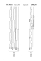
- an inverted signal which would conventionally beindicated by a line over the signal identification will be represented by the identification of the signal followed by [inv].
- the TWD control signal (9A) from the common equipment must be inverted and delayedby about 40 nanoseconds at the Transmit Clock falling edge.
- a TWD Control unit 66 which includes a D flip-flop, which performs the inversion and synch function, and a CMOS gate unit which addsthe delay.
- TXSLOT provides the 8 bit transmission window (9E) for the CODEC and includes a Dflip-flop and an AND gate which received TSQ and TSP.
- the window begins on the next rising edge of TWDl after TSQ (9D) and TSPA(B) (9C) from bank commons are pulled high.
- the window ends with the next rising edge of TWDlwhen TSQ and TSPA(B) are low. During this window, beginning at the first clock rising edge, eight data bits are shifted out by the codec.
- the ASK signal from detection circuit 34 is received by ASK signal control circuit 70, along with TXSLOT[inv].
- the 8 bit data shifted out by the codec is sent to a mixer 72 having two AND gates and one OR gate which substitutes the LSB according to the LSB status as indicated by the ASK signal control circuit 70.
- a high indicates an absence of ASK and a low indicates its presence.
- a counter provides the timing sequence to locate the LSB every 125 microseconds.
- Circuit 70 includes a D flip-flop, an AND gate and one OR gate which change the state of the LSB depending on the presence or absence of ASK signals.
- TXLSBCTL is generated by a logic low of TXSLOT[inv]. This triggers a 4 bit counter, LSB control circuit 71, on the next clock rising edge until the 8th clock cycle. The output TXLSBCTL then goes high to enable LSB transmission.
- the TXLSBCTL pulse has an approximate duration of one clock cycle repeated every 125 microseconds.
- control data receive circuit 40 referring to FIGS. 8, 10 and 11, a nine bit shift is required to locate the 8 bits of RNDATA into the RXSLOT[inv] window which is accomplished by an 8 bit shift register followed by 2 D flip-flops which each shift the data 1/2 bit.
- RXSLOT[inv] is initiated on the next RWD rising edge when RSQ and RSPA (orRSPB, depending on which channel is being discussed) are pulled high as seen in FIG. 10.
- RXDATA is simultaneously transmitted to the codec and LSBcontrol circuits.
- the analog output of codec and the 8 kHz oscillator are summed by an operational amplifier.
- An LSB control circuit 76 includes a counter to produce a RXLSBCTL (ReceiveLeast Significant Bit Control) pulse every 125 microseconds with the occurrence of RXSLOT "low” and the 8th falling edge clock cycle of RXCLK and a D flip-flop then latches the LSB.
- the D flip-flop generates ASKCTL and its inverse which are used to control two analog switches for 8 kHz generation.
- a RXLSBCTL (Receive Least Significant Bit Control) pulse is provided to latch LSB at a D flip-flop 75.
- the signal ASKCTL[inv] is provided by the D flip-flop 75.
- the duration of RXLSBCTL isequal to one-half clock cycle.
- An ASK feedback control circuit 74 includes a counter and two NAND gates which provide a delay of about 312 microseconds (2.5 frames) to provide aninput to the OR gate in circuit 70 so that the ASK signal from detector 34 can go through the OR gate to the flip-flop in circuit 70. When that inputis not present, the ASK signal generated in the receive circuit is locked out to prevent potential feedback in the opposite direction.
- frame refers to the time window defined by TXCTL and "sample” refers to the 8th bit window. A high on RXSLOT[inv] resets the counter.
- the sine wave generator includes an oscillator circuit 78 which receives a clock signal of 1.544 MHz and produces a 1.536 MB/s pulse train which is fed into a counter and an AND gate arranged to produce an 8 kHz pulse.
- a Dflip-flop 80 is used to combine that 8 kHz pulse with the RXLSBCTL pulse toprovide an 8 kHz square wave signal.
- the sine wave conversion is accomplished by a bandpass active filter 82.
- the sine wave zero-crossing level is then synchronized with the rising and falling edge of the output of the D flip-flop 80.
- the signal at the output of the analog switch 84 an 8 kHz sine wave, will start at zero crossing level for the ODD channel but will represent a 30° lag on EVEN channel due to the fact that signal synchronizationis provided by the ODD channel.
Abstract
Description
y=1n(1+u|x|)/1n(1+u)
(24 channels×8 bits/channel+1 frame bit)×8000 Hz=1.544 Mbit/s
Claims (5)
Priority Applications (3)
| Application Number | Priority Date | Filing Date | Title |
|---|---|---|---|
| US07/238,617 US4901344A (en) | 1988-08-31 | 1988-08-31 | Telephone system digital channel bank interface |
| CA000608740A CA1320556C (en) | 1988-08-31 | 1989-08-18 | Telephone system digital channel bank interface |
| US07/456,944 US4987573A (en) | 1988-08-31 | 1989-12-26 | Telephone system digital channel bank interface |
Applications Claiming Priority (1)
| Application Number | Priority Date | Filing Date | Title |
|---|---|---|---|
| US07/238,617 US4901344A (en) | 1988-08-31 | 1988-08-31 | Telephone system digital channel bank interface |
Related Child Applications (1)
| Application Number | Title | Priority Date | Filing Date |
|---|---|---|---|
| US07/456,944 Continuation US4987573A (en) | 1988-08-31 | 1989-12-26 | Telephone system digital channel bank interface |
Publications (1)
| Publication Number | Publication Date |
|---|---|
| US4901344A true US4901344A (en) | 1990-02-13 |
Family
ID=22898652
Family Applications (1)
| Application Number | Title | Priority Date | Filing Date |
|---|---|---|---|
| US07/238,617 Expired - Lifetime US4901344A (en) | 1988-08-31 | 1988-08-31 | Telephone system digital channel bank interface |
Country Status (2)
| Country | Link |
|---|---|
| US (1) | US4901344A (en) |
| CA (1) | CA1320556C (en) |
Cited By (14)
| Publication number | Priority date | Publication date | Assignee | Title |
|---|---|---|---|---|
| US4987573A (en) * | 1988-08-31 | 1991-01-22 | Pulsecom Division Of Hubbell Incorporated | Telephone system digital channel bank interface |
| US5016246A (en) * | 1989-12-29 | 1991-05-14 | Hubbell Incorporated | Digital telephone system circuits |
| US5027341A (en) * | 1990-03-30 | 1991-06-25 | Charter Leasing Corporation | Station line switching control system |
| US5146457A (en) * | 1988-09-16 | 1992-09-08 | U.S. Philips Corporation | Device for transmitting data words representing a digitalized analog signal and device for receiving the transmitted data words |
| US5263081A (en) * | 1989-11-01 | 1993-11-16 | Hubbell Incorporated | Method and apparatus for providing on-hook transmission for digital loop carrier channel units |
| US5278899A (en) * | 1992-04-02 | 1994-01-11 | Hubbell Incorporated | Digital telephone system noise reduction circuit |
| US5347566A (en) * | 1991-10-23 | 1994-09-13 | Digital Transmission Systems, Inc. | Retrofit subscriber loop carrier system with improved performance monitoring and remote provisioning |
| US5412709A (en) * | 1992-06-24 | 1995-05-02 | Charter Leasing Corporation | Digital telephone station line controller |
| US5574783A (en) * | 1995-11-22 | 1996-11-12 | Lucent Technologies Inc. | System and method for providing competitive access telephone service for telephones connected to a remote terminal of the monopoly service provider |
| US5610922A (en) * | 1995-03-20 | 1997-03-11 | Raychem Corporation | Voice plus 4-wire DDS multiplexer |
| US5668814A (en) * | 1995-03-20 | 1997-09-16 | Raychem Corporation | Dual DDS data multiplexer |
| US5940408A (en) * | 1996-08-01 | 1999-08-17 | Adtran, Inc. | Use of redundant bits of ESF data stream to transport message-waiting signalling over FXO/FXS T-1 digital link |
| US6282204B1 (en) | 1997-12-19 | 2001-08-28 | Terayon Communication Systems, Inc. | ISDN plus voice multiplexer system |
| US20140153667A1 (en) * | 2012-12-05 | 2014-06-05 | Electronics And Telecommunications Research Institute | Apparatus and method for transmitting and receiving signal of ofdm system |
Citations (5)
| Publication number | Priority date | Publication date | Assignee | Title |
|---|---|---|---|---|
| US3748393A (en) * | 1970-02-17 | 1973-07-24 | Int Standard Electric Corp | Data transmission over pulse code modulation channels |
| US4151373A (en) * | 1976-09-09 | 1979-04-24 | Gretag Aktiengesellschaft | Data transmission system |
| US4171467A (en) * | 1978-07-20 | 1979-10-16 | Bell Telephone Laboratories, Incorporated | Signal multiplexing circuit |
| US4292474A (en) * | 1979-08-13 | 1981-09-29 | Oki Electronics Of America, Inc. | Electronic key telephone system with bi-directional serial data stream station control |
| US4750173A (en) * | 1985-05-21 | 1988-06-07 | Polygram International Holding B.V. | Method of transmitting audio information and additional information in digital form |
-
1988
- 1988-08-31 US US07/238,617 patent/US4901344A/en not_active Expired - Lifetime
-
1989
- 1989-08-18 CA CA000608740A patent/CA1320556C/en not_active Expired - Fee Related
Patent Citations (5)
| Publication number | Priority date | Publication date | Assignee | Title |
|---|---|---|---|---|
| US3748393A (en) * | 1970-02-17 | 1973-07-24 | Int Standard Electric Corp | Data transmission over pulse code modulation channels |
| US4151373A (en) * | 1976-09-09 | 1979-04-24 | Gretag Aktiengesellschaft | Data transmission system |
| US4171467A (en) * | 1978-07-20 | 1979-10-16 | Bell Telephone Laboratories, Incorporated | Signal multiplexing circuit |
| US4292474A (en) * | 1979-08-13 | 1981-09-29 | Oki Electronics Of America, Inc. | Electronic key telephone system with bi-directional serial data stream station control |
| US4750173A (en) * | 1985-05-21 | 1988-06-07 | Polygram International Holding B.V. | Method of transmitting audio information and additional information in digital form |
Non-Patent Citations (2)
| Title |
|---|
| Bellamy, John, "Digital Telephony", pp. 101-102. |
| Bellamy, John, Digital Telephony , pp. 101 102. * |
Cited By (16)
| Publication number | Priority date | Publication date | Assignee | Title |
|---|---|---|---|---|
| US4987573A (en) * | 1988-08-31 | 1991-01-22 | Pulsecom Division Of Hubbell Incorporated | Telephone system digital channel bank interface |
| US5146457A (en) * | 1988-09-16 | 1992-09-08 | U.S. Philips Corporation | Device for transmitting data words representing a digitalized analog signal and device for receiving the transmitted data words |
| US5263081A (en) * | 1989-11-01 | 1993-11-16 | Hubbell Incorporated | Method and apparatus for providing on-hook transmission for digital loop carrier channel units |
| US5016246A (en) * | 1989-12-29 | 1991-05-14 | Hubbell Incorporated | Digital telephone system circuits |
| US5027341A (en) * | 1990-03-30 | 1991-06-25 | Charter Leasing Corporation | Station line switching control system |
| US5347566A (en) * | 1991-10-23 | 1994-09-13 | Digital Transmission Systems, Inc. | Retrofit subscriber loop carrier system with improved performance monitoring and remote provisioning |
| US5278899A (en) * | 1992-04-02 | 1994-01-11 | Hubbell Incorporated | Digital telephone system noise reduction circuit |
| US5412709A (en) * | 1992-06-24 | 1995-05-02 | Charter Leasing Corporation | Digital telephone station line controller |
| US5978390A (en) * | 1995-03-20 | 1999-11-02 | Raychem Corporation | Dual DDS data multiplexer |
| US5610922A (en) * | 1995-03-20 | 1997-03-11 | Raychem Corporation | Voice plus 4-wire DDS multiplexer |
| US5668814A (en) * | 1995-03-20 | 1997-09-16 | Raychem Corporation | Dual DDS data multiplexer |
| US5574783A (en) * | 1995-11-22 | 1996-11-12 | Lucent Technologies Inc. | System and method for providing competitive access telephone service for telephones connected to a remote terminal of the monopoly service provider |
| US5940408A (en) * | 1996-08-01 | 1999-08-17 | Adtran, Inc. | Use of redundant bits of ESF data stream to transport message-waiting signalling over FXO/FXS T-1 digital link |
| US6282204B1 (en) | 1997-12-19 | 2001-08-28 | Terayon Communication Systems, Inc. | ISDN plus voice multiplexer system |
| US20140153667A1 (en) * | 2012-12-05 | 2014-06-05 | Electronics And Telecommunications Research Institute | Apparatus and method for transmitting and receiving signal of ofdm system |
| US8982988B2 (en) * | 2012-12-05 | 2015-03-17 | Electronics And Telecommunications Research Institute | Apparatus and method for transmitting and receiving signal of OFDM system |
Also Published As
| Publication number | Publication date |
|---|---|
| CA1320556C (en) | 1993-07-20 |
Similar Documents
| Publication | Publication Date | Title |
|---|---|---|
| US4627047A (en) | Integrated voice and data telecommunication switching system | |
| CA1186077A (en) | Interleaved digital data and voice communications system apparatus and method | |
| US5276678A (en) | Distributed switching and telephone conferencing system | |
| US4750169A (en) | Telephone system and method for transmitting digital information | |
| US6240179B1 (en) | Voice and data communications | |
| CN1119009C (en) | Secure access telephone extension system and method | |
| US4901344A (en) | Telephone system digital channel bank interface | |
| US5263081A (en) | Method and apparatus for providing on-hook transmission for digital loop carrier channel units | |
| US5014306A (en) | Voice and data telephone communication system and method | |
| US4402073A (en) | Speech and data communication network | |
| US4271509A (en) | Supervisory signaling for digital channel banks | |
| US4839888A (en) | Digital time-division multiplex switch-based telephone subscriber connection system | |
| US4809260A (en) | Telephone exchange | |
| US4987573A (en) | Telephone system digital channel bank interface | |
| GB2221123A (en) | Digital telephone system | |
| US4566096A (en) | Telephone exchange conference circuit | |
| US3435149A (en) | Tone generators for delta modulation time division communication switching systems | |
| US5278899A (en) | Digital telephone system noise reduction circuit | |
| Griffiths | ISDN network terminating equipment | |
| US6307870B1 (en) | Process for transmitting digitized payload and signalling data over a channel | |
| CA2309272C (en) | Telephone network for a structured item and telephone communication between remote structured items using this system | |
| McDonald | Techniques for digital switching | |
| GB2072463A (en) | Speech and data communication network | |
| Jain | Fundamentals of Telecommunications | |
| Dahlbom | Signaling systems and technology |
Legal Events
| Date | Code | Title | Description |
|---|---|---|---|
| AS | Assignment |
Owner name: 156721 CANADA INCORPORATED, 1282 RUE DES CYPRES, P Free format text: ASSIGNMENT OF ASSIGNORS INTEREST.;ASSIGNORS:MONETTE, JEAN-YVES;DESABRAIS, SYLVAIN;REEL/FRAME:004933/0292 Effective date: 19880824 |
|
| STCF | Information on status: patent grant |
Free format text: PATENTED CASE |
|
| AS | Assignment |
Owner name: PULSECOM DIVISION, HUBBELL INCORPORATED, A CORP. Free format text: ASSIGNMENT OF ASSIGNORS INTEREST.;ASSIGNOR:156721 CANADA INC.;REEL/FRAME:005379/0790 Effective date: 19900718 |
|
| FEPP | Fee payment procedure |
Free format text: PAYOR NUMBER ASSIGNED (ORIGINAL EVENT CODE: ASPN); ENTITY STATUS OF PATENT OWNER: LARGE ENTITY |
|
| FPAY | Fee payment |
Year of fee payment: 4 |
|
| FPAY | Fee payment |
Year of fee payment: 8 |
|
| FPAY | Fee payment |
Year of fee payment: 12 |
|
| AS | Assignment |
Owner name: PULSE COMMUNICATIONS, INC., VIRGINIA Free format text: ASSIGNMENT OF ASSIGNORS INTEREST;ASSIGNOR:PULSECOM DIVISION OF HUBBELL INCORPORATED;REEL/FRAME:014901/0543 Effective date: 20040113 |