US4854670A - Wide angle optical filters - Google Patents
Wide angle optical filters Download PDFInfo
- Publication number
- US4854670A US4854670A US07/178,790 US17879088A US4854670A US 4854670 A US4854670 A US 4854670A US 17879088 A US17879088 A US 17879088A US 4854670 A US4854670 A US 4854670A
- Authority
- US
- United States
- Prior art keywords
- coating
- filter
- design wavelength
- refractive index
- thickness
- Prior art date
- Legal status (The legal status is an assumption and is not a legal conclusion. Google has not performed a legal analysis and makes no representation as to the accuracy of the status listed.)
- Expired - Lifetime
Links
- 230000003287 optical effect Effects 0.000 title claims abstract description 33
- 238000013461 design Methods 0.000 claims abstract description 26
- 239000010409 thin film Substances 0.000 claims abstract description 15
- 238000000576 coating method Methods 0.000 claims description 49
- 239000011248 coating agent Substances 0.000 claims description 38
- VYPSYNLAJGMNEJ-UHFFFAOYSA-N Silicium dioxide Chemical compound O=[Si]=O VYPSYNLAJGMNEJ-UHFFFAOYSA-N 0.000 claims description 26
- 239000000463 material Substances 0.000 claims description 26
- GWEVSGVZZGPLCZ-UHFFFAOYSA-N Titan oxide Chemical compound O=[Ti]=O GWEVSGVZZGPLCZ-UHFFFAOYSA-N 0.000 claims description 22
- 239000000758 substrate Substances 0.000 claims description 15
- 239000000377 silicon dioxide Substances 0.000 claims description 13
- 235000012239 silicon dioxide Nutrition 0.000 claims description 12
- 239000004408 titanium dioxide Substances 0.000 claims description 10
- 239000011521 glass Substances 0.000 claims 1
- 238000004519 manufacturing process Methods 0.000 abstract description 12
- 230000005540 biological transmission Effects 0.000 abstract description 5
- 238000000034 method Methods 0.000 abstract description 5
- 230000000694 effects Effects 0.000 abstract 1
- 238000000151 deposition Methods 0.000 description 20
- 230000008021 deposition Effects 0.000 description 19
- OGIDPMRJRNCKJF-UHFFFAOYSA-N titanium oxide Inorganic materials [Ti]=O OGIDPMRJRNCKJF-UHFFFAOYSA-N 0.000 description 13
- QVGXLLKOCUKJST-UHFFFAOYSA-N atomic oxygen Chemical compound [O] QVGXLLKOCUKJST-UHFFFAOYSA-N 0.000 description 8
- 229910052760 oxygen Inorganic materials 0.000 description 8
- 239000001301 oxygen Substances 0.000 description 8
- 230000008901 benefit Effects 0.000 description 5
- 238000002834 transmittance Methods 0.000 description 4
- 238000013459 approach Methods 0.000 description 3
- 238000005137 deposition process Methods 0.000 description 3
- 238000005566 electron beam evaporation Methods 0.000 description 3
- 230000009286 beneficial effect Effects 0.000 description 2
- 238000004891 communication Methods 0.000 description 2
- 238000005094 computer simulation Methods 0.000 description 2
- 238000001816 cooling Methods 0.000 description 2
- 239000006185 dispersion Substances 0.000 description 2
- 238000001704 evaporation Methods 0.000 description 2
- 230000008020 evaporation Effects 0.000 description 2
- 239000010408 film Substances 0.000 description 2
- 238000010438 heat treatment Methods 0.000 description 2
- 238000012544 monitoring process Methods 0.000 description 2
- KELHQGOVULCJSG-UHFFFAOYSA-N n,n-dimethyl-1-(5-methylfuran-2-yl)ethane-1,2-diamine Chemical compound CN(C)C(CN)C1=CC=C(C)O1 KELHQGOVULCJSG-UHFFFAOYSA-N 0.000 description 2
- 238000001771 vacuum deposition Methods 0.000 description 2
- -1 NL =1.48 Substances 0.000 description 1
- 239000005083 Zinc sulfide Substances 0.000 description 1
- 239000005388 borosilicate glass Substances 0.000 description 1
- 229910052792 caesium Inorganic materials 0.000 description 1
- TVFDJXOCXUVLDH-UHFFFAOYSA-N caesium atom Chemical compound [Cs] TVFDJXOCXUVLDH-UHFFFAOYSA-N 0.000 description 1
- 229910052681 coesite Inorganic materials 0.000 description 1
- 238000012937 correction Methods 0.000 description 1
- 229910052906 cristobalite Inorganic materials 0.000 description 1
- 229910001610 cryolite Inorganic materials 0.000 description 1
- 230000003247 decreasing effect Effects 0.000 description 1
- 230000003292 diminished effect Effects 0.000 description 1
- 238000005516 engineering process Methods 0.000 description 1
- 238000001914 filtration Methods 0.000 description 1
- 238000002329 infrared spectrum Methods 0.000 description 1
- ORUIBWPALBXDOA-UHFFFAOYSA-L magnesium fluoride Chemical compound [F-].[F-].[Mg+2] ORUIBWPALBXDOA-UHFFFAOYSA-L 0.000 description 1
- 229910001635 magnesium fluoride Inorganic materials 0.000 description 1
- KJLLKLRVCJAFRY-UHFFFAOYSA-N mebutizide Chemical compound ClC1=C(S(N)(=O)=O)C=C2S(=O)(=O)NC(C(C)C(C)CC)NC2=C1 KJLLKLRVCJAFRY-UHFFFAOYSA-N 0.000 description 1
- 238000012986 modification Methods 0.000 description 1
- 230000004048 modification Effects 0.000 description 1
- 230000003647 oxidation Effects 0.000 description 1
- 238000007254 oxidation reaction Methods 0.000 description 1
- 229910052682 stishovite Inorganic materials 0.000 description 1
- MZQZQKZKTGRQCG-UHFFFAOYSA-J thorium tetrafluoride Chemical compound F[Th](F)(F)F MZQZQKZKTGRQCG-UHFFFAOYSA-J 0.000 description 1
- 229910052905 tridymite Inorganic materials 0.000 description 1
- 229910052984 zinc sulfide Inorganic materials 0.000 description 1
- DRDVZXDWVBGGMH-UHFFFAOYSA-N zinc;sulfide Chemical group [S-2].[Zn+2] DRDVZXDWVBGGMH-UHFFFAOYSA-N 0.000 description 1
Images


Classifications
-
- G—PHYSICS
- G02—OPTICS
- G02B—OPTICAL ELEMENTS, SYSTEMS OR APPARATUS
- G02B5/00—Optical elements other than lenses
- G02B5/20—Filters
- G02B5/28—Interference filters
- G02B5/281—Interference filters designed for the infrared light
- G02B5/282—Interference filters designed for the infrared light reflecting for infrared and transparent for visible light, e.g. heat reflectors, laser protection
Definitions
- the present invention is directed to a thin-film optical interference filter designed and manufactured to have high-transmittance of blue light and high reflectance of infrared light.
- Optical interference filters of the long-wave pass and short-wave pass types are normally based upon quarterwave stacks. See, for example, H. A. Macleod, "Thin-film Optical Filters,” American Elsevier, N.Y. (1969).
- a quarterwave stack generally consists of alternating layers or "series" of high-reflectance materials and low-reflectance materials. See, for example, A. Thelen, "Equivalent Layers in Multilayer Filters,” J. Opt. Soc. Am.. 50:1533-1538 (1966). See also U.S. Pat. No. 2,412,496, issued Dec. 10, 1946, to Dimmick.
- halfwave hole One problem typically encountered in the use of optical filters based upon quarterwave stacks is known as a "halfwave hole.”
- the halfwave holes appear as dips or minima in the transmittance curve, occurring especially at incident angles approaching 50°. See, H. A. Macleod, "Performance Limiting Factors in Optical Coatings," Proceedings of the Los Alamos Conference on Optics, '81, D. H. Liebenberg, ed., SPIE, 288:580-586 (1981).
- a layer which appears as a quarterwave at 900 nm does not necessarily appear as a halfwave at 450 nm. This is due to the fact that the film's refractive index may increase at shorter wavelengths. Since the variation in refractive index is generally less for low-index layers, this variation causes a distinction between the wavelength for which the high-index layers are halfwaves from that for which the low-index layers are halfwaves. Thus, the high-and low-index layers are not halfwaves at the same wavelength, and a "hole" appears.
- the present invention provides an alternate solution to the halfwave hole phenomenon.
- the present invention is directed to a thin-film optical interference filter which provides a high-transmission of blue light and high-reflectance of infrared light.
- the thin-film layer of the present invention suppresses the halfwave hole problem which occurs at wide angles of incidence of the incoming light. This desirable result is achieved by a combination of the proper layer thicknesses and refractive-index control in the manufacturing process.
- FIGS. 1 and 2 represent the computed reflectance of the thin-film interference filter of the present invention, in contrast to the computed reflectance of a typical quarterwave stack of the prior art shown in FIGS. 3 and 4.
- the percent reflectance is shown versus wavelength, where reflectance is the percentage of light not transmitted through the filter.
- FIGS. 1 and 2 the reflectance at 0 and 53 degrees angle of incidence respectively, is illustrated for the filter of the present invention.
- FIGS. 3 and 4 the reflectance at 0 and 53 degrees angle of incidence respectively, is illustrated for a typical quarterwave stack from the prior art.
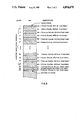
- FIG. 5 is an enlarged cross-sectional view of a thin-film optical interference filter in accordance with the invention.
- a filter in accordance with the invention is designed in part to reflect infrared light or wavelengths in the range of approximately 850-900 nm at angles of incidence of 0° to approximately 55°. Accordingly, the design wavelength, to which the term “quarterwave” pertains, is approximately 880 nm.
- the abbreviation "nm” is used herein to denote a nanometer which is one billionth of a meter or ten Angstroms.
- the quarterwave stack portion of this design for example, layers 2-24, inclusive, of FIG. 5, is known in the art of interference coating technology.
- the new features of the stack of the present invention are the layers at the top and bottom of the stack, e.g., layer 1 in FIG. 5 at the top and layers 25-27 in FIG. 5 at the bottom, as well as the novel method of fabricating the filter.
- FIGS. 1 and 2 represent the computed reflectance of a preferred thin-film interference filter of the present invention.
- FIGS. 3 and 4 represent the computed reflectance of a typical quarterwave stack from the prior art.
- FIGS. 1 and 3 are based on the model that the incident light is normal to the filter.
- the light approaches the filter at an angle of incidence of 53 degrees from the normal.
- the percentage reflectance of the invention is substantially less than that of the prior art for light having wavelengths ranging between approximately 430 to approximately 480 nm which may be characterized herein as blue light.
- a thin-film optical filter in accordance with the invention approximately 95% or more of blue light passes through the filter, whereas comparable quarterwave optical filters of the prior art typically transmit a maximum of 85% of blue light.
- the blue-light transmittance advantage of the invention improves with greater angles of incidence of the incoming light up to approximately 55 degrees angle of incidence.
- the ability to transmit a high percentage of blue light at wide angles is advantageous in various applications including pre-filtering of atomic resonance communications devices. Using this new design and the manufacturing process described below to prepare same, a cost effective system for manufacturing wide-band optical filters, especially useful in undersea communications devices, has been achieved.
- the manufacture of a filter in accordance with the invention may be conducted using a low-refractive index material, preferably silicon dioxide, and a high-refractive index material, preferably titanium dioxide.
- the layers are deposited, for example, by a known electron beam evaporation technique in a high-vacuum coating machine with planetary substrate tooling. Other conventional deposition techniques may be employed, but electron beam evaporation is the preferred method.
- an index of refraction will be characterized as being "low” if it is less than or equal to 1.6; as “intermediate,” if greater than 1.6 and less than 1.9; and as "high,” if greater than or equal to 1.9, for filters designed to operate in the visible and near-infrared spectra.
- the substrate is maintained at an elevated temperature, e.g., at or above 200° C.
- the refractive index of titanium dioxide is affected by the partial pressure of oxygen, the total pressure in the coating machine, and the rate of deposition; so that by careful monitoring of these parameters during the deposition process, reproducible control of the index of refraction for each layer may be achieved.
- Filter size is not a constraint, so long as the physical orientation of the evaporation sources to the substrate is maintained and the coating machine is well instrumented so that proper coating conditions are maintained.
- the fabrication of the optical coating is performed by applying successive layers commencing at the substrate at the "bottom” of the stack and ending at the "top” of the stack; see, for example, FIG. 5.
- the top two layers preferably both of silicon dioxide
- layers 1 and 2 of FIG. 5 are produced by interrupting the deposition process, so that two layers of the same low-refractive index material are created. This may be accomplished, for example, by stopping deposition, allowing the substrate to cool, e.g., to about 100° C., and then resuming deposition.
- the interruption is preferably conducted for only a short period, for example, for about 5 minutes. This creates an optical boundary defining the two adjacent layers of silicon dioxide.
- layer 1 should have a thickness of approximately 25% to approximately 67% of the thickness of layer 2 in order to observe improved transmission of blue light through the filter.
- layer 2 is the top most layer of the quarterwave stack (see FIG. 5).
- the gist of the novel method of fabrication of a thin-film optical filter is as follows.
- An optical boundary is formed between two adjacent layers of the same coating material by applying a first coating on the substrate (or on another coating of the filter) at a first temperature and then applying a second coating of the same material on the first coating at a second temperature.
- this involves four steps as follows: (a) heating or cooling the substrate to a first temperature; (b) applying the first coating of material at a first temperature to attain a first coating thickness; (c) heating or cooling the substrate to a second temperature; and (d) applying the second coating of the same material at a second temperature to attain a second coating thickness.
- the second deposition temperature is cooler than the first temperature so that step (c) is accomplished simply by interrupting the coating process for a period sufficient to allow the substrate to cool to the second deposition temperature.
- deposition temperature is the critical control parameter.
- layer 1 has an index of refraction of approximately 1.43 and layer 2 has an index of refraction of approximately 1.48.
- layer 1 is believed to act in combination with layer 2 to minimize reflectance of blue light in a way analogous to that of an ideal decreasing graded index layer.
- layers 25-27 of FIG. 5 provide an optical interface between the substrate and quarterwave stack which minimizes reflectance of blue light particularly at higher angles of incidence up to approximately 55 degrees.
- Layers 25-27 of FIG. 5 comprise a layer of a low-refractive index material, such as silicon dioxide, sandwiched between two substantially thinner layers of a high-refractive index material, such as titanium dioxide. Experimentation has demonstrated that this combination of layer materials and thicknesses at the bottom of the stack maximizes the ability of the filter to transmit blue light at high angles of incidence.
- the thicknesses of layers 25 and 27 were varied from approximately 1/64 to 1/32 of the design wavelength. All examples demonstrated beneficial results, i.e., improved transmission of blue light through the filter. There is no requirement that layers 25 and 27 have equal thicknesses. It is believed that a layer or layers thinner than 1/64 of the design wavelength would provide beneficial results provided uniform layer thickness can be effectively fabricated. Observations indicate that benefits diminished rapidly when the layer thickness exceeded 1/32 of the design wavelength.
- the middle layer i.e., layer 26 of FIG. 5, had a thickness of one-eighth of the design wavelength, plus or minus ten percent of one-eighth of the design wavelength. In all cases, the benefits of the invention were observed as reported.
- the layers were deposited by electron beam evaporation in a high-vacuum coating machine with planetary tooling. During evaporation, oxygen was introduced into the system so that titanium dioxide was formed by oxidation of vaporized titanium monoxide.
- the substrate temperature was maintained at about 200° C. throughout the deposition of the quarterwave stack.
- the substrate material was borosilicate glass.
- the top two stack layers of silicon dioxide were produced by interrupting the deposition, so that two layers of the same material with an optical boundary therebetween were created. This was accomplished by stopping the deposition process, allowing the system to cool from 200° C. to about 100° C., and then resuming deposition. The interruption was conducted for about 5 minutes. This created the desired optical boundary.
- the refractive index of layer 2 of silicon dioxide was approximately 1.48
- the refractive index of the layer 1 of silicon dioxide was approximately 1.43.
- the layers of the preferred optical filter of the present invention and their respective coating parameters are set forth in Table I below.
- N is the index of refraction.
- D is coating thickness.
- D (monitor) is the coating thickness on an Inficon IC-6000 thickness monitor.
- D (filter) is the actual coating thickness on the borosilicate substrate.
- D (optical) is the design thickness, measured in fractions of the design wavelength.
- Rate is the rate of deposition measured by the Inficon monitor in nanometers per second.
- Oxygen pressure is the partial pressure of oxygen admitted to the coating machine in units of 10 -4 Torr.
- Total pressure is the total pressure within the coating machine in units of 10 -4 Torr.
- SiO 2 is an abbreviation for silicon dioxide
- TiO 2 is an abbreviation for titanium dioxide.
- Another high-index material that may be employed in place of titanium dioxide is zinc sulfide.
- Other possible low-index materials are magnesium fluoride, cryolite (but not with titanium dioxide), and thorium fluoride. These suggested alternate materials are intended as examples and by no means comprise an exhaustive list.
- FIGS. 1 and 3 show the performance of this embodiment of the invention. As commented on above, the filter transmits a substantially higher percentage of blue light than its prior art counterparts while having high reflectance of infrared wavelengths.
Abstract
A thin-film optical interference filter designed and manufactured to have high transmission of blue light and high reflectance of infrared light. The novel feature of this filter rests in the thin-film layer design at the top and bottom of a quarterwave stack and the manufacturing technique by which this thin-film design is deposited. The thin-film layer design suppresses the so called halfwave holes which occur at wide angles of incidence of the incoming light. This desirable effect is achieved by the proper layer thickness and refractive index control in the manufacturing process.
Description
The Government of the United States of America has certain rights in this invention pursuant to Contract No. N00039-84-C0643, Subcontract SD03-01531, with the United States Navy.
p This is a continuation-in-part of Ser. No. 943,274, filed Dec. 17, 1986, assigned to the assignee hereof now abandoned.
The present invention is directed to a thin-film optical interference filter designed and manufactured to have high-transmittance of blue light and high reflectance of infrared light.
Optical interference filters of the long-wave pass and short-wave pass types are normally based upon quarterwave stacks. See, for example, H. A. Macleod, "Thin-film Optical Filters," American Elsevier, N.Y. (1969).
A quarterwave stack generally consists of alternating layers or "series" of high-reflectance materials and low-reflectance materials. See, for example, A. Thelen, "Equivalent Layers in Multilayer Filters," J. Opt. Soc. Am.. 50:1533-1538 (1966). See also U.S. Pat. No. 2,412,496, issued Dec. 10, 1946, to Dimmick.
One problem typically encountered in the use of optical filters based upon quarterwave stacks is known as a "halfwave hole." The halfwave holes appear as dips or minima in the transmittance curve, occurring especially at incident angles approaching 50°. See, H. A. Macleod, "Performance Limiting Factors in Optical Coatings," Proceedings of the Los Alamos Conference on Optics, '81, D. H. Liebenberg, ed., SPIE, 288:580-586 (1981).
The nature of the halfwave holes is such that monitoring errors, which cause departure from the strict halfwave thickness of the layers, invariably lead to transmittance dips in the transmission band. No satisfactory compensation for wide-angle filters has been discovered for this error, which must be kept as small as possible.
Another cause of a halfwave hole is layer dispersion. A layer which appears as a quarterwave at 900 nm does not necessarily appear as a halfwave at 450 nm. This is due to the fact that the film's refractive index may increase at shorter wavelengths. Since the variation in refractive index is generally less for low-index layers, this variation causes a distinction between the wavelength for which the high-index layers are halfwaves from that for which the low-index layers are halfwaves. Thus, the high-and low-index layers are not halfwaves at the same wavelength, and a "hole" appears.
One approach to solving the "halfwave hole" problem includes ensuring that, in spite of dispersion, the layers are halfwaves at precisely the same wavelengths. This approach strives to eliminate thickness errors as far as possible. An optical interference filter incorporating these corrections was disclosed in a report entitled "SLC Cesium Atomic Resonance Filter Interference Coatings," by H. A. Macleod et al., Final Report for Navy Contract No. N66001-82K-0187 (September 1983).
The present invention provides an alternate solution to the halfwave hole phenomenon.
The present invention is directed to a thin-film optical interference filter which provides a high-transmission of blue light and high-reflectance of infrared light.
The unique features of this filter rest in the thin-film layer design and the manufacturing technique by which this film is deposited.
The thin-film layer of the present invention suppresses the halfwave hole problem which occurs at wide angles of incidence of the incoming light. This desirable result is achieved by a combination of the proper layer thicknesses and refractive-index control in the manufacturing process.
The novel coating design and fabrication method of the present invention is described in the detailed description which follows, infra.
FIGS. 1 and 2 represent the computed reflectance of the thin-film interference filter of the present invention, in contrast to the computed reflectance of a typical quarterwave stack of the prior art shown in FIGS. 3 and 4. In each figure, the percent reflectance is shown versus wavelength, where reflectance is the percentage of light not transmitted through the filter.
In FIGS. 1 and 2, the reflectance at 0 and 53 degrees angle of incidence respectively, is illustrated for the filter of the present invention.
In FIGS. 3 and 4, the reflectance at 0 and 53 degrees angle of incidence respectively, is illustrated for a typical quarterwave stack from the prior art.
FIG. 5 is an enlarged cross-sectional view of a thin-film optical interference filter in accordance with the invention.
A filter in accordance with the invention is designed in part to reflect infrared light or wavelengths in the range of approximately 850-900 nm at angles of incidence of 0° to approximately 55°. Accordingly, the design wavelength, to which the term "quarterwave" pertains, is approximately 880 nm. The abbreviation "nm" is used herein to denote a nanometer which is one billionth of a meter or ten Angstroms.
The quarterwave stack portion of this design, for example, layers 2-24, inclusive, of FIG. 5, is known in the art of interference coating technology. The new features of the stack of the present invention are the layers at the top and bottom of the stack, e.g., layer 1 in FIG. 5 at the top and layers 25-27 in FIG. 5 at the bottom, as well as the novel method of fabricating the filter.
FIGS. 1 and 2 represent the computed reflectance of a preferred thin-film interference filter of the present invention. FIGS. 3 and 4 represent the computed reflectance of a typical quarterwave stack from the prior art. FIGS. 1 and 3 are based on the model that the incident light is normal to the filter. In FIGS. 2 and 4, the light approaches the filter at an angle of incidence of 53 degrees from the normal. As may be seen from comparisons of FIGS. 1 and 3 and FIGS. 2 and 4, respectively, the percentage reflectance of the invention is substantially less than that of the prior art for light having wavelengths ranging between approximately 430 to approximately 480 nm which may be characterized herein as blue light.
In a thin-film optical filter in accordance with the invention, approximately 95% or more of blue light passes through the filter, whereas comparable quarterwave optical filters of the prior art typically transmit a maximum of 85% of blue light. The blue-light transmittance advantage of the invention improves with greater angles of incidence of the incoming light up to approximately 55 degrees angle of incidence. The ability to transmit a high percentage of blue light at wide angles is advantageous in various applications including pre-filtering of atomic resonance communications devices. Using this new design and the manufacturing process described below to prepare same, a cost effective system for manufacturing wide-band optical filters, especially useful in undersea communications devices, has been achieved.
The manufacture of a filter in accordance with the invention may be conducted using a low-refractive index material, preferably silicon dioxide, and a high-refractive index material, preferably titanium dioxide. The layers are deposited, for example, by a known electron beam evaporation technique in a high-vacuum coating machine with planetary substrate tooling. Other conventional deposition techniques may be employed, but electron beam evaporation is the preferred method. For purposes herein, an index of refraction will be characterized as being "low" if it is less than or equal to 1.6; as "intermediate," if greater than 1.6 and less than 1.9; and as "high," if greater than or equal to 1.9, for filters designed to operate in the visible and near-infrared spectra.
During the coating process, an ample supply of oxygen is maintained within the coating machine. This insures that the vaporized titanium monoxide will combine with oxygen and condense into a titanium dioxide layer. During deposition, the substrate is maintained at an elevated temperature, e.g., at or above 200° C.
It is known that the refractive index of titanium dioxide is affected by the partial pressure of oxygen, the total pressure in the coating machine, and the rate of deposition; so that by careful monitoring of these parameters during the deposition process, reproducible control of the index of refraction for each layer may be achieved.
Filter size is not a constraint, so long as the physical orientation of the evaporation sources to the substrate is maintained and the coating machine is well instrumented so that proper coating conditions are maintained.
The fabrication of the optical coating is performed by applying successive layers commencing at the substrate at the "bottom" of the stack and ending at the "top" of the stack; see, for example, FIG. 5. The top two layers (preferably both of silicon dioxide), i.e., layers 1 and 2 of FIG. 5, are produced by interrupting the deposition process, so that two layers of the same low-refractive index material are created. This may be accomplished, for example, by stopping deposition, allowing the substrate to cool, e.g., to about 100° C., and then resuming deposition. The interruption is preferably conducted for only a short period, for example, for about 5 minutes. This creates an optical boundary defining the two adjacent layers of silicon dioxide. At this boundary, optical light interference occurs which minimizes reflection and maximizes transmission of blue light through the filter. Experimental results show that layer 1 should have a thickness of approximately 25% to approximately 67% of the thickness of layer 2 in order to observe improved transmission of blue light through the filter. Note, layer 2 is the top most layer of the quarterwave stack (see FIG. 5).
The gist of the novel method of fabrication of a thin-film optical filter is as follows. An optical boundary is formed between two adjacent layers of the same coating material by applying a first coating on the substrate (or on another coating of the filter) at a first temperature and then applying a second coating of the same material on the first coating at a second temperature. In practice, this involves four steps as follows: (a) heating or cooling the substrate to a first temperature; (b) applying the first coating of material at a first temperature to attain a first coating thickness; (c) heating or cooling the substrate to a second temperature; and (d) applying the second coating of the same material at a second temperature to attain a second coating thickness. It is not critical whether the second deposition temperature is greater or less than the first deposition temperature as long as the two deposition temperatures are different. Because the two adjacent coatings are applied at different deposition temperatures, the respective densities and refractive indices of the two coatings are also different, notwithstanding the fact that the two coatings are of the same material, whereby an "optical boundary" between the coatings has been defined. In the preferred embodiment described herein, the second deposition temperature is cooler than the first temperature so that step (c) is accomplished simply by interrupting the coating process for a period sufficient to allow the substrate to cool to the second deposition temperature. As will be seen, other deposition parameters, such as the deposition pressure and deposition rate, may be varied between the application of the two coatings; however, it is believed that deposition temperature is the critical control parameter.
In a preferred embodiment of the present invention employing silicon dioxide in the top two stack layers, layer 1 has an index of refraction of approximately 1.43 and layer 2 has an index of refraction of approximately 1.48. Thus, layer 1 is believed to act in combination with layer 2 to minimize reflectance of blue light in a way analogous to that of an ideal decreasing graded index layer.
The three layers at the bottom of the stack, i.e., layers 25-27 of FIG. 5, provide an optical interface between the substrate and quarterwave stack which minimizes reflectance of blue light particularly at higher angles of incidence up to approximately 55 degrees. Layers 25-27 of FIG. 5 comprise a layer of a low-refractive index material, such as silicon dioxide, sandwiched between two substantially thinner layers of a high-refractive index material, such as titanium dioxide. Experimentation has demonstrated that this combination of layer materials and thicknesses at the bottom of the stack maximizes the ability of the filter to transmit blue light at high angles of incidence.
In laboratory examples, the thicknesses of layers 25 and 27 were varied from approximately 1/64 to 1/32 of the design wavelength. All examples demonstrated beneficial results, i.e., improved transmission of blue light through the filter. There is no requirement that layers 25 and 27 have equal thicknesses. It is believed that a layer or layers thinner than 1/64 of the design wavelength would provide beneficial results provided uniform layer thickness can be effectively fabricated. Observations indicate that benefits diminished rapidly when the layer thickness exceeded 1/32 of the design wavelength.
In the laboratory examples investigated, the middle layer, i.e., layer 26 of FIG. 5, had a thickness of one-eighth of the design wavelength, plus or minus ten percent of one-eighth of the design wavelength. In all cases, the benefits of the invention were observed as reported.
Laboratory examples further demonstrate that the benefits of the invention are enhanced when the invention includes the combination of the top-most layer of the stack, the three layers at the bottom of the stack, and the intermediate quarterwave stack; this combination is the preferred embodiment described herein. However, substantial benefits may be obtained by employing the three layers at the bottom of the stack and the quarterwave stack without the layer above the quarterwave stack.
The present invention will be further illustrated with reference to the following example which aids in its understanding, but which is not to be construed as a limitation thereof.
Manufacture of the preferred filter of the present invention was conducted using silicon dioxide as the low-refractive index material, NL =1.48, and titanium dioxide as the high-refractive index material, NH =1.9 to 2.3, where N is the index of refraction.
The layers were deposited by electron beam evaporation in a high-vacuum coating machine with planetary tooling. During evaporation, oxygen was introduced into the system so that titanium dioxide was formed by oxidation of vaporized titanium monoxide.
The substrate temperature was maintained at about 200° C. throughout the deposition of the quarterwave stack. The substrate material was borosilicate glass.
The top two stack layers of silicon dioxide were produced by interrupting the deposition, so that two layers of the same material with an optical boundary therebetween were created. This was accomplished by stopping the deposition process, allowing the system to cool from 200° C. to about 100° C., and then resuming deposition. The interruption was conducted for about 5 minutes. This created the desired optical boundary. The refractive index of layer 2 of silicon dioxide was approximately 1.48, and the refractive index of the layer 1 of silicon dioxide was approximately 1.43.
The layers of the preferred optical filter of the present invention and their respective coating parameters are set forth in Table I below. In this Table, "N" is the index of refraction. "D" is coating thickness. "D (monitor)" is the coating thickness on an Inficon IC-6000 thickness monitor. "D (filter)" is the actual coating thickness on the borosilicate substrate. "D (optical)" is the design thickness, measured in fractions of the design wavelength. "Rate" is the rate of deposition measured by the Inficon monitor in nanometers per second. "Oxygen pressure" is the partial pressure of oxygen admitted to the coating machine in units of 10-4 Torr. "Total pressure" is the total pressure within the coating machine in units of 10-4 Torr. SiO2 is an abbreviation for silicon dioxide, and TiO2 is an abbreviation for titanium dioxide.
In the Table, values for D (monitor), Rate, Oxygen Pressure, and Total Pressure are observed values. Values for N, D (optical), and D (filter) were obtained from a computer simulation. These values are believed to be accurate because the observed filter performance was consistent with the performance predicted by the computer simulation. The lower indices of refraction in layers 25 and 27 are the result of the lower deposition rates required to attain the extreme thinness of these layers.
Another high-index material that may be employed in place of titanium dioxide is zinc sulfide. Other possible low-index materials are magnesium fluoride, cryolite (but not with titanium dioxide), and thorium fluoride. These suggested alternate materials are intended as examples and by no means comprise an exhaustive list.
FIGS. 1 and 3 show the performance of this embodiment of the invention. As commented on above, the filter transmits a substantially higher percentage of blue light than its prior art counterparts while having high reflectance of infrared wavelengths.
The present invention has been described in detail, including the preferred embodiments thereof. However, it will be appreciated that those skilled in the art, upon consideration of the present disclosure, may make modifications and/or improvements on this invention and still be within the scope and spirit of this invention as set forth in the following claims.
                                  TABLE I
__________________________________________________________________________
EXAMPLE COATING PARAMETERS
                                    Oxygen
                                          Total
            D (monitor)
                   D (filter)
                        D (optical)
                               Rate Pressure
                                          Pressure
Layer
    Material
         N  (nm)   (nm) (wavelength)
                               (nm/sec)
                                    (10.sup.-4 Torr)
                                          (10.sup.-4 Torr)
__________________________________________________________________________
(Top of Stack)
1   SiO.sub.2
         1.43
            109.2  82.5 0.125  1.5  1.6   2.6
2   SiO.sub.2
         1.48
            219.1  165.5
                        0.25   1.5  1.6   2.6
3   TiO.sub.2
         2.25
            136.1  108.9
                        0.25   1.2  2.1   2.6
4   SiO.sub.2
         1.48
            219.1  165.5
                        0.25   1.5  1.6   2.6
5   TiO.sub.2
         2.25
            136.1  108.9
                        0.25   1.2  2.1   2.6
6   SiO.sub.2
         1.48
            219.1  165.5
                        0.25   1.5  1.6   2.6
7   TiO.sub.2
         2.25
            136.1  108.9
                        0.25   1.2  2.1   2.6
8   SiO.sub.2
         1.48
            219.1  165.5
                        0.25   1.5  1.6   2.6
9   TiO.sub.2
         2.25
            136.1  108.9
                        0.25   1.2  2.1   2.6
10  SiO.sub.2
         1.48
            219.1  165.5
                        0.25   1.5  1.6   2.6
11  TiO.sub.2
         2.25
            136.1  108.9
                        0.25   1.2  2.1   2.6
12  SiO.sub.2
         1.48
            219.1  165.5
                        0.25   1.5  1.6   2.6
13  TiO.sub.2
         2.25
            136.1  108.9
                        0.25   1.2  2.1   2.6
14  SiO.sub.2
         1.48
            219.1  165.5
                        0.25   1.5  1.6   2.6
15  TiO.sub.2
         2.25
            136.1  108.9
                        0.25   1.2  2.1   2.6
16  SiO.sub.2
         1.48
            219.1  165.5
                        0.25   1.5  1.6   2.6
17  TiO.sub.2
         2.25
            136.1  108.9
                        0.25   1.2  2.1   2.6
18  SiO.sub.2
         1.48
            219.1  165.5
                        0.25   1.5  1.6   2.6
19  TiO.sub.2
         2.25
            136.1  108.9
                        0.25   1.2  2.1   2.6
20  SiO.sub.2
         1.48
            219.1  165.5
                        0.25   1.5  1.6   2.6
21  TiO.sub.2
         2.25
            136.1  108.9
                        0.25   1.2  2.1   2.6
22  SiO.sub.2
         1.48
            219.1  165.5
                        0.25   1.5  1.6   2.6
23  TiO.sub.2
         2.25
            136.1  108.9
                        0.25   1.2  2.1   2.6
24  SiO.sub.2
         1.48
            219.1  165.5
                        0.25   1.5  1.6   2.6
25  TiO.sub.2
         2.10
            7.9    6.3  0.015  0.2  2.1   2.6
26  SiO.sub.2
         1.48
            109.8  82.9 0.125  1.5  1.6   2.6
27  TiO.sub.2
         2.10
            7.9    6.3  0.015  0.2  2.1   2.6
(Bottom of Stack)
__________________________________________________________________________
Claims (7)
1. A thin-film optical interference filter having high-transmission of blue light and high-reflectance of infrared light, said filter having a predetermined design wavelength, said filter comprising:
(a) a glass substrate;
(b) a first or bottom coating of a high-refractive index material applied on said substrate, said first coating having a first thickness of less than one-sixteenth of said design wavelength;
(c) a second coating of a low-refractive index material applied on said first coating, said second coating having a second thickness greater than one-sixteenth and less than three-sixteenths of said design wavelength;
(d) a third coating of a high-refractive index material applied on said second coating, said third coating having a third thickness of less than one-sixteenth of said design wavelength; and
(e) a quarterwave stack applied on said third coating, said quarterwave stack including a plurality of layers of alternating high- and low-refractive index materials, said quarterwave stack having a design wavelength being matched approximately to said predetermined design wavelength of said filter.
2. An optical filter as described in claim 1 wherein said filter further includes a fourth coating of low-refractive index material applied on said quarterwave stack, said fourth coating having a thickness of less than one-quarter of said design wavelength.
3. An optical filter as described in claim 1 wherein said first and third coatings are formed from titanium dioxide and said second coating is formed from silicon dioxide.
4. An optical filter as described in claim 2 wherein said fourth coating is formed from silicon dioxide.
5. An optical filter as described in claim 1 wherein the thicknesses of said first and third coatings are each less than one thirty-second of said design wavelength and the thickness of said second coating is one-eighth of said design wavelength plus or minus one-tenth of one-eighth of said wavelength.
6. An optical filter as described in claim 2 wherein the thickness of said fourth coating is between approximately twenty-five percent to approximately sixty-seven percent of one-quarter of said design wavelength.
7. An optical filter as described in claim 1 wherein said design wavelength is approximately 880 nanometers.
Priority Applications (1)
| Application Number | Priority Date | Filing Date | Title |
|---|---|---|---|
| US07/178,790 US4854670A (en) | 1986-12-17 | 1988-03-29 | Wide angle optical filters |
Applications Claiming Priority (2)
| Application Number | Priority Date | Filing Date | Title |
|---|---|---|---|
| US94327486A | 1986-12-17 | 1986-12-17 | |
| US07/178,790 US4854670A (en) | 1986-12-17 | 1988-03-29 | Wide angle optical filters |
Related Parent Applications (1)
| Application Number | Title | Priority Date | Filing Date |
|---|---|---|---|
| US94327486A Continuation-In-Part | 1986-12-17 | 1986-12-17 |
Related Child Applications (1)
| Application Number | Title | Priority Date | Filing Date |
|---|---|---|---|
| US07/248,675 Division US4931315A (en) | 1986-12-17 | 1988-09-23 | Wide angle optical filters |
Publications (1)
| Publication Number | Publication Date |
|---|---|
| US4854670A true US4854670A (en) | 1989-08-08 |
Family
ID=26874651
Family Applications (1)
| Application Number | Title | Priority Date | Filing Date |
|---|---|---|---|
| US07/178,790 Expired - Lifetime US4854670A (en) | 1986-12-17 | 1988-03-29 | Wide angle optical filters |
Country Status (1)
| Country | Link |
|---|---|
| US (1) | US4854670A (en) |
Cited By (27)
| Publication number | Priority date | Publication date | Assignee | Title |
|---|---|---|---|---|
| US5035485A (en) * | 1988-12-23 | 1991-07-30 | Minolta Camera Kabushiki Kaisha | Interference filter with sharp cutoff characteristics |
| US5076675A (en) * | 1988-02-26 | 1991-12-31 | Fujitsu Limited | Polarizing separating device and optical isolator employing the same |
| WO1992016875A2 (en) * | 1991-03-20 | 1992-10-01 | Costich Verne R | Infrared filter |
| US5177396A (en) * | 1990-12-19 | 1993-01-05 | Gte Products Corporation | Mirror with dichroic coating lamp housing |
| US5179468A (en) * | 1991-11-05 | 1993-01-12 | Gte Products Corporation | Interleaving of similar thin-film stacks for producing optical interference coatings |
| US5246767A (en) * | 1988-12-13 | 1993-09-21 | Mitsui Petrochemical Industries, Ltd. | High light-transmissive dust-proof body and method of preparing same |
| US5246803A (en) * | 1990-07-23 | 1993-09-21 | Eastman Kodak Company | Patterned dichroic filters for solid state electronic image sensors |
| US5348805A (en) * | 1990-07-05 | 1994-09-20 | Saint-Gobain Vitrage International | Formation of a layer of aluminum and tin or titanium oxides on a glass substrate |
| US5378892A (en) * | 1990-09-28 | 1995-01-03 | Martin Marietta Corporation | Angle filter for use in an infrared optical system |
| US5513039A (en) * | 1993-05-26 | 1996-04-30 | Litton Systems, Inc. | Ultraviolet resistive coated mirror and method of fabrication |
| US5550423A (en) * | 1993-12-08 | 1996-08-27 | Osram Sylvania Inc. | Optical coating and lamp employing same |
| US5705882A (en) * | 1995-10-20 | 1998-01-06 | Osram Sylvania Inc. | Optical coating and lamp employing same |
| US5814367A (en) * | 1993-08-13 | 1998-09-29 | General Atomics | Broadband infrared and signature control materials and methods of producing the same |
| WO2000031572A1 (en) * | 1998-11-25 | 2000-06-02 | Minnesota Mining And Manufacturing Company | Multilayer reflector with enhanced acceptance angle and selective transmission |
| US6139968A (en) * | 1995-03-08 | 2000-10-31 | Corion Corporation | Multilayer ion plated coatings comprising titanium oxide |
| US6235105B1 (en) | 1994-12-06 | 2001-05-22 | General Atomics | Thin film pigmented optical coating compositions |
| WO2002005291A2 (en) * | 2000-07-10 | 2002-01-17 | Technische Universität | Optical component |
| WO2002061469A2 (en) * | 2001-01-15 | 2002-08-08 | 3M Innovative Properties Company | Multilayer infrared reflecting film with high and smooth transmission in visible wavelength region and laminate articles made therefrom |
| WO2007077658A1 (en) * | 2005-12-28 | 2007-07-12 | Murata Manufacturing Co., Ltd. | Terahertz-band optical filter, its designing method, and its manufacturing method |
| US20090075067A1 (en) * | 2007-09-14 | 2009-03-19 | Cardinal Cg Company | Low-maintenance coating technology |
| US7862910B2 (en) | 2006-04-11 | 2011-01-04 | Cardinal Cg Company | Photocatalytic coatings having improved low-maintenance properties |
| US20120212809A1 (en) * | 2011-02-23 | 2012-08-23 | Asia Optical Co., Inc. | Infrared Cut Filter |
| USRE43817E1 (en) | 2004-07-12 | 2012-11-20 | Cardinal Cg Company | Low-maintenance coatings |
| US9738967B2 (en) | 2006-07-12 | 2017-08-22 | Cardinal Cg Company | Sputtering apparatus including target mounting and control |
| US10604442B2 (en) | 2016-11-17 | 2020-03-31 | Cardinal Cg Company | Static-dissipative coating technology |
| US11131794B2 (en) | 2012-07-16 | 2021-09-28 | Viavi Solutions Inc. | Optical filter and sensor system |
| US11714219B2 (en) | 2018-08-14 | 2023-08-01 | Platinum Optics Technology Inc. | Infrared band pass filter having layers with refraction index greater than 3.5 |
Citations (4)
| Publication number | Priority date | Publication date | Assignee | Title |
|---|---|---|---|---|
| US2412496A (en) * | 1945-06-30 | 1946-12-10 | Rca Corp | Color selective reflector |
| US4461532A (en) * | 1981-04-30 | 1984-07-24 | Nippon Soken, Inc. | Heat rays reflecting film |
| US4504109A (en) * | 1981-11-25 | 1985-03-12 | Kabushiki Kaisha Toyota Chuo Kenkyusho | Infrared shielding lamination |
| US4556599A (en) * | 1982-05-20 | 1985-12-03 | Nippon Soken, Inc. | Heat reflection film |
-
1988
- 1988-03-29 US US07/178,790 patent/US4854670A/en not_active Expired - Lifetime
Patent Citations (4)
| Publication number | Priority date | Publication date | Assignee | Title |
|---|---|---|---|---|
| US2412496A (en) * | 1945-06-30 | 1946-12-10 | Rca Corp | Color selective reflector |
| US4461532A (en) * | 1981-04-30 | 1984-07-24 | Nippon Soken, Inc. | Heat rays reflecting film |
| US4504109A (en) * | 1981-11-25 | 1985-03-12 | Kabushiki Kaisha Toyota Chuo Kenkyusho | Infrared shielding lamination |
| US4556599A (en) * | 1982-05-20 | 1985-12-03 | Nippon Soken, Inc. | Heat reflection film |
Cited By (46)
| Publication number | Priority date | Publication date | Assignee | Title |
|---|---|---|---|---|
| US5076675A (en) * | 1988-02-26 | 1991-12-31 | Fujitsu Limited | Polarizing separating device and optical isolator employing the same |
| US5246767A (en) * | 1988-12-13 | 1993-09-21 | Mitsui Petrochemical Industries, Ltd. | High light-transmissive dust-proof body and method of preparing same |
| US5035485A (en) * | 1988-12-23 | 1991-07-30 | Minolta Camera Kabushiki Kaisha | Interference filter with sharp cutoff characteristics |
| US5348805A (en) * | 1990-07-05 | 1994-09-20 | Saint-Gobain Vitrage International | Formation of a layer of aluminum and tin or titanium oxides on a glass substrate |
| US5246803A (en) * | 1990-07-23 | 1993-09-21 | Eastman Kodak Company | Patterned dichroic filters for solid state electronic image sensors |
| US5378892A (en) * | 1990-09-28 | 1995-01-03 | Martin Marietta Corporation | Angle filter for use in an infrared optical system |
| US5177396A (en) * | 1990-12-19 | 1993-01-05 | Gte Products Corporation | Mirror with dichroic coating lamp housing |
| US5426532A (en) * | 1991-03-20 | 1995-06-20 | Costich; Verne R. | Infrared filter |
| WO1992016875A2 (en) * | 1991-03-20 | 1992-10-01 | Costich Verne R | Infrared filter |
| WO1992016875A3 (en) * | 1991-03-20 | 1992-10-29 | Verne R Costich | Infrared filter |
| US5233464A (en) * | 1991-03-20 | 1993-08-03 | Costich Verne R | Multilayer infrared filter |
| US5179468A (en) * | 1991-11-05 | 1993-01-12 | Gte Products Corporation | Interleaving of similar thin-film stacks for producing optical interference coatings |
| US5513039A (en) * | 1993-05-26 | 1996-04-30 | Litton Systems, Inc. | Ultraviolet resistive coated mirror and method of fabrication |
| US5814367A (en) * | 1993-08-13 | 1998-09-29 | General Atomics | Broadband infrared and signature control materials and methods of producing the same |
| US6288837B1 (en) | 1993-08-13 | 2001-09-11 | General Atomics | Broadband infrared and signature control materials and methods of producing the same |
| US5550423A (en) * | 1993-12-08 | 1996-08-27 | Osram Sylvania Inc. | Optical coating and lamp employing same |
| US6235105B1 (en) | 1994-12-06 | 2001-05-22 | General Atomics | Thin film pigmented optical coating compositions |
| US6139968A (en) * | 1995-03-08 | 2000-10-31 | Corion Corporation | Multilayer ion plated coatings comprising titanium oxide |
| US5705882A (en) * | 1995-10-20 | 1998-01-06 | Osram Sylvania Inc. | Optical coating and lamp employing same |
| WO2000031572A1 (en) * | 1998-11-25 | 2000-06-02 | Minnesota Mining And Manufacturing Company | Multilayer reflector with enhanced acceptance angle and selective transmission |
| US6208466B1 (en) | 1998-11-25 | 2001-03-27 | 3M Innovative Properties Company | Multilayer reflector with selective transmission |
| WO2002005291A3 (en) * | 2000-07-10 | 2002-06-27 | Tech Uni | Optical component |
| US20040075923A1 (en) * | 2000-07-10 | 2004-04-22 | Pascal Knobloch | Optical component |
| WO2002005291A2 (en) * | 2000-07-10 | 2002-01-17 | Technische Universität | Optical component |
| US6954309B2 (en) | 2000-07-10 | 2005-10-11 | Technische Universität Braunschweig Carolo-Wilhelmina | Optical component |
| KR100905142B1 (en) | 2001-01-15 | 2009-06-29 | 쓰리엠 이노베이티브 프로퍼티즈 컴파니 | Multilayer Infrared Reflecting Film With High and Smooth Transmission in Visible Wavelength Region and Laminate Articles Made Therefrom |
| US6927900B2 (en) | 2001-01-15 | 2005-08-09 | 3M Innovative Properties Company | Multilayer infrared reflecting film with high and smooth transmission in visible wavelength region and laminate articles made therefrom |
| WO2002061469A3 (en) * | 2001-01-15 | 2002-10-10 | 3M Innovative Properties Co | Multilayer infrared reflecting film with high and smooth transmission in visible wavelength region and laminate articles made therefrom |
| WO2002061469A2 (en) * | 2001-01-15 | 2002-08-08 | 3M Innovative Properties Company | Multilayer infrared reflecting film with high and smooth transmission in visible wavelength region and laminate articles made therefrom |
| USRE43817E1 (en) | 2004-07-12 | 2012-11-20 | Cardinal Cg Company | Low-maintenance coatings |
| USRE44155E1 (en) | 2004-07-12 | 2013-04-16 | Cardinal Cg Company | Low-maintenance coatings |
| WO2007077658A1 (en) * | 2005-12-28 | 2007-07-12 | Murata Manufacturing Co., Ltd. | Terahertz-band optical filter, its designing method, and its manufacturing method |
| US20080252979A1 (en) * | 2005-12-28 | 2008-10-16 | Murata Manufacturing Co., Ltd. | Terahertz-Band Optical Filter, Designing Method Thereof, and Manufacturing Method Thereof |
| US7573639B2 (en) | 2005-12-28 | 2009-08-11 | Murata Manufacturing Co., Ltd | Terahertz-band optical filter, designing method thereof, and manufacturing method thereof |
| US7862910B2 (en) | 2006-04-11 | 2011-01-04 | Cardinal Cg Company | Photocatalytic coatings having improved low-maintenance properties |
| US9738967B2 (en) | 2006-07-12 | 2017-08-22 | Cardinal Cg Company | Sputtering apparatus including target mounting and control |
| US7820296B2 (en) | 2007-09-14 | 2010-10-26 | Cardinal Cg Company | Low-maintenance coating technology |
| US7820309B2 (en) | 2007-09-14 | 2010-10-26 | Cardinal Cg Company | Low-maintenance coatings, and methods for producing low-maintenance coatings |
| US8506768B2 (en) | 2007-09-14 | 2013-08-13 | Cardinal Cg Company | Low-maintenance coatings, and methods for producing low-maintenance coatings |
| US8696879B2 (en) | 2007-09-14 | 2014-04-15 | Cardinal Cg Company | Low-maintenance coating technology |
| US20090075067A1 (en) * | 2007-09-14 | 2009-03-19 | Cardinal Cg Company | Low-maintenance coating technology |
| US20120212809A1 (en) * | 2011-02-23 | 2012-08-23 | Asia Optical Co., Inc. | Infrared Cut Filter |
| US11131794B2 (en) | 2012-07-16 | 2021-09-28 | Viavi Solutions Inc. | Optical filter and sensor system |
| US10604442B2 (en) | 2016-11-17 | 2020-03-31 | Cardinal Cg Company | Static-dissipative coating technology |
| US11325859B2 (en) | 2016-11-17 | 2022-05-10 | Cardinal Cg Company | Static-dissipative coating technology |
| US11714219B2 (en) | 2018-08-14 | 2023-08-01 | Platinum Optics Technology Inc. | Infrared band pass filter having layers with refraction index greater than 3.5 |
Similar Documents
| Publication | Publication Date | Title |
|---|---|---|
| US4854670A (en) | Wide angle optical filters | |
| US4931315A (en) | Wide angle optical filters | |
| US5993898A (en) | Fabrication method and structure for multilayer optical anti-reflection coating, and optical component and optical system using multilayer optical anti-reflection coating | |
| US20050219724A1 (en) | Optical element having a dielectric multilayer film | |
| US10459124B2 (en) | Layer system and optical element comprising a layer system | |
| US20080144166A1 (en) | IR absorbing reflector | |
| KR100496557B1 (en) | Method for producing composition for vapor deposition, composition for vapor deposition, and method for producing optical element with antireflection film | |
| EP2437084A1 (en) | Optical lens with anti-scratch, anti-reflective layer | |
| US10131571B2 (en) | Methods of forming optical system components and optical coatings | |
| PT1184685E (en) | Optical element having anti-reflection film | |
| JP2003050311A (en) | Attenuating filter for ultraviolet light | |
| DE2738044C2 (en) | Lens made from a synthetic polymer | |
| US20220373723A1 (en) | Optical element having a protective coating, method for the production thereof and optical arrangement | |
| US7875305B2 (en) | Thin film filter having negative temperature drift coefficient | |
| Lemarquis et al. | Broadband antireflection coatings for visible and infrared ranges | |
| CN211263842U (en) | 2050nm laser polarizing film | |
| US5879820A (en) | Multilayer stack of fluoride materials usable in optics and its production process | |
| Scherer et al. | High performance notch filter coatings produced with PIAD and magnetron sputtering | |
| JP2022173188A (en) | porous thin film | |
| KR101918768B1 (en) | Hafnium oxide or zirconium oxide coating | |
| WO1991008106A1 (en) | Antireflection layer system with integral uv blocking properties | |
| Johnson | Bandpass Filters Past and Present | |
| RU209445U1 (en) | OPTICAL MIRROR | |
| KR960013791B1 (en) | Optical device | |
| RU2778680C1 (en) | Optical mirror |
Legal Events
| Date | Code | Title | Description |
|---|---|---|---|
| AS | Assignment |
Owner name: GTE PRODUCTS CORPORATION, A DE CORP. Free format text: ASSIGNMENT OF ASSIGNORS INTEREST.;ASSIGNOR:MELLOR, CHARLES E.;REEL/FRAME:004898/0214 Effective date: 19880328 |
|
| STCF | Information on status: patent grant |
Free format text: PATENTED CASE |
|
| FEPP | Fee payment procedure |
Free format text: PAYOR NUMBER ASSIGNED (ORIGINAL EVENT CODE: ASPN); ENTITY STATUS OF PATENT OWNER: LARGE ENTITY |
|
| FPAY | Fee payment |
Year of fee payment: 4 |
|
| FPAY | Fee payment |
Year of fee payment: 8 |
|
| FPAY | Fee payment |
Year of fee payment: 12 |