US4685197A - Fabricating a stacked capacitor - Google Patents
Fabricating a stacked capacitor Download PDFInfo
- Publication number
- US4685197A US4685197A US06/781,846 US78184686A US4685197A US 4685197 A US4685197 A US 4685197A US 78184686 A US78184686 A US 78184686A US 4685197 A US4685197 A US 4685197A
- Authority
- US
- United States
- Prior art keywords
- plates
- conductive plates
- etched
- capacitor
- conductive
- Prior art date
- Legal status (The legal status is an assumption and is not a legal conclusion. Google has not performed a legal analysis and makes no representation as to the accuracy of the status listed.)
- Expired - Fee Related
Links
- 239000003990 capacitor Substances 0.000 title claims abstract description 34
- 238000000034 method Methods 0.000 claims abstract description 38
- 238000005530 etching Methods 0.000 claims description 15
- 239000000758 substrate Substances 0.000 claims description 11
- ZAMOUSCENKQFHK-UHFFFAOYSA-N Chlorine atom Chemical compound [Cl] ZAMOUSCENKQFHK-UHFFFAOYSA-N 0.000 claims description 3
- ZOKXTWBITQBERF-UHFFFAOYSA-N Molybdenum Chemical compound [Mo] ZOKXTWBITQBERF-UHFFFAOYSA-N 0.000 claims description 3
- GRYLNZFGIOXLOG-UHFFFAOYSA-N Nitric acid Chemical compound O[N+]([O-])=O GRYLNZFGIOXLOG-UHFFFAOYSA-N 0.000 claims description 3
- XAGFODPZIPBFFR-UHFFFAOYSA-N aluminium Chemical compound [Al] XAGFODPZIPBFFR-UHFFFAOYSA-N 0.000 claims description 3
- 229910052782 aluminium Inorganic materials 0.000 claims description 3
- 229910052801 chlorine Inorganic materials 0.000 claims description 3
- 239000000460 chlorine Substances 0.000 claims description 3
- 229910052750 molybdenum Inorganic materials 0.000 claims description 3
- 239000011733 molybdenum Substances 0.000 claims description 3
- 229910017604 nitric acid Inorganic materials 0.000 claims description 3
- 229910021420 polycrystalline silicon Inorganic materials 0.000 claims description 3
- WFKWXMTUELFFGS-UHFFFAOYSA-N tungsten Chemical compound [W] WFKWXMTUELFFGS-UHFFFAOYSA-N 0.000 claims description 3
- 229910052721 tungsten Inorganic materials 0.000 claims description 3
- 239000010937 tungsten Substances 0.000 claims description 3
- 230000000873 masking effect Effects 0.000 claims 4
- 239000012811 non-conductive material Substances 0.000 claims 4
- 239000002253 acid Substances 0.000 claims 2
- 239000003989 dielectric material Substances 0.000 abstract description 6
- 238000004519 manufacturing process Methods 0.000 abstract description 6
- 239000000463 material Substances 0.000 abstract description 6
- 238000005229 chemical vapour deposition Methods 0.000 description 9
- 238000010586 diagram Methods 0.000 description 6
- 229920002120 photoresistant polymer Polymers 0.000 description 6
- VYPSYNLAJGMNEJ-UHFFFAOYSA-N Silicium dioxide Chemical compound O=[Si]=O VYPSYNLAJGMNEJ-UHFFFAOYSA-N 0.000 description 4
- 239000004020 conductor Substances 0.000 description 3
- KRHYYFGTRYWZRS-UHFFFAOYSA-N Fluorane Chemical compound F KRHYYFGTRYWZRS-UHFFFAOYSA-N 0.000 description 2
- 239000012212 insulator Substances 0.000 description 2
- 235000012239 silicon dioxide Nutrition 0.000 description 2
- 239000000377 silicon dioxide Substances 0.000 description 2
- YCKRFDGAMUMZLT-UHFFFAOYSA-N Fluorine atom Chemical compound [F] YCKRFDGAMUMZLT-UHFFFAOYSA-N 0.000 description 1
- 239000000654 additive Substances 0.000 description 1
- 230000000996 additive effect Effects 0.000 description 1
- 238000010420 art technique Methods 0.000 description 1
- 230000015572 biosynthetic process Effects 0.000 description 1
- 229910021419 crystalline silicon Inorganic materials 0.000 description 1
- 230000001419 dependent effect Effects 0.000 description 1
- 238000000151 deposition Methods 0.000 description 1
- 229910052731 fluorine Inorganic materials 0.000 description 1
- 239000011737 fluorine Substances 0.000 description 1
- 239000007788 liquid Substances 0.000 description 1
- 239000000126 substance Substances 0.000 description 1
Images


Classifications
-
- H—ELECTRICITY
- H10—SEMICONDUCTOR DEVICES; ELECTRIC SOLID-STATE DEVICES NOT OTHERWISE PROVIDED FOR
- H10B—ELECTRONIC MEMORY DEVICES
- H10B12/00—Dynamic random access memory [DRAM] devices
- H10B12/01—Manufacture or treatment
- H10B12/02—Manufacture or treatment for one transistor one-capacitor [1T-1C] memory cells
- H10B12/03—Making the capacitor or connections thereto
-
- H—ELECTRICITY
- H01—ELECTRIC ELEMENTS
- H01L—SEMICONDUCTOR DEVICES NOT COVERED BY CLASS H10
- H01L28/00—Passive two-terminal components without a potential-jump or surface barrier for integrated circuits; Details thereof; Multistep manufacturing processes therefor
- H01L28/40—Capacitors
-
- H—ELECTRICITY
- H01—ELECTRIC ELEMENTS
- H01L—SEMICONDUCTOR DEVICES NOT COVERED BY CLASS H10
- H01L29/00—Semiconductor devices adapted for rectifying, amplifying, oscillating or switching, or capacitors or resistors with at least one potential-jump barrier or surface barrier, e.g. PN junction depletion layer or carrier concentration layer; Details of semiconductor bodies or of electrodes thereof ; Multistep manufacturing processes therefor
- H01L29/66—Types of semiconductor device ; Multistep manufacturing processes therefor
- H01L29/86—Types of semiconductor device ; Multistep manufacturing processes therefor controllable only by variation of the electric current supplied, or only the electric potential applied, to one or more of the electrodes carrying the current to be rectified, amplified, oscillated or switched
- H01L29/92—Capacitors with potential-jump barrier or surface barrier
- H01L29/94—Metal-insulator-semiconductors, e.g. MOS
- H01L29/945—Trench capacitors
-
- H—ELECTRICITY
- H10—SEMICONDUCTOR DEVICES; ELECTRIC SOLID-STATE DEVICES NOT OTHERWISE PROVIDED FOR
- H10B—ELECTRONIC MEMORY DEVICES
- H10B12/00—Dynamic random access memory [DRAM] devices
- H10B12/30—DRAM devices comprising one-transistor - one-capacitor [1T-1C] memory cells
-
- H—ELECTRICITY
- H10—SEMICONDUCTOR DEVICES; ELECTRIC SOLID-STATE DEVICES NOT OTHERWISE PROVIDED FOR
- H10B—ELECTRONIC MEMORY DEVICES
- H10B99/00—Subject matter not provided for in other groups of this subclass
-
- Y—GENERAL TAGGING OF NEW TECHNOLOGICAL DEVELOPMENTS; GENERAL TAGGING OF CROSS-SECTIONAL TECHNOLOGIES SPANNING OVER SEVERAL SECTIONS OF THE IPC; TECHNICAL SUBJECTS COVERED BY FORMER USPC CROSS-REFERENCE ART COLLECTIONS [XRACs] AND DIGESTS
- Y10—TECHNICAL SUBJECTS COVERED BY FORMER USPC
- Y10T—TECHNICAL SUBJECTS COVERED BY FORMER US CLASSIFICATION
- Y10T29/00—Metal working
- Y10T29/43—Electric condenser making
- Y10T29/435—Solid dielectric type
Definitions
- the present invention relates to the field of integrated circuit fabrication. More specifically, the present invention relates to a structure and method for fabricating capacitors in integrated circuits.
- the described embodiments of present invention provides a structure, and method for fabricating that structure, which provides increased capacitance over the prior art while occupying a minimum of surface area of the integrated circuit.
- the present invention accomplishes this by interleaving multiple capacitor plates to provide increased capacitance while occupying the same surface area as a prior art capacitor which provides a fraction of the capacitance provided by the present invention.
- the present invention is fabricated by providing a capacitor stack which includes interleaved plates of material which may be selectively etched and which are separated by appropriate dielectric material. One portion of the stack is masked while one set of the interleaved plates is etched. The etched portion of the interleave plates is filled by a suitable dielectric and a contact is made to the remaining plates.
- a different portion of the stack is then exposed to an etch which etches the other set of interleaved plates.
- the area etched away is then filled with a suitable dielectric and a contact is made to the unetched interleaved plates.
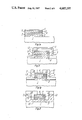
- FIGS. 1A through 1G are side view schematic diagrams depicting the processing steps of this invention which provide one embodiment of the structure of this invention
- FIG. 2 is another embodiment of the present invention using a different plate contact scheme
- FIG. 4 is a side view schematic diagram depicting one embodiment of the invention including multiple interleaved plates.
- FIGS. 1A through 1G are side view schematic diagrams depicting the processing steps of one embodiment of this invention used to fabricate a structure which is another embodiment of the present invention.
- dielectric layer 2 is formed on the surface of substrate 1 using techniques well known in the art such as chemical vapor deposition.
- Substrate 1 may be a crystalline silicon substrate so that other components well known in the art of integrated circuit manufacturing may be fabricated therein.
- Dielectric layer 2 may be any suitable dielectric such as silicon dioxide.
- Conductor layer 3 is formed on the surface of dielectric layer 2 using techniques well known in the art such as chemical vapor deposition.
- Conductive layer 3 is formed of a material such as molybdenum which may be selectively etched while not etching dielectric layer 2.
- Dielectric layer 4 is formed on the surface of conductive layer 3 using techniques well known in the art such as chemical vapor deposition.
- Dielectric layer 4 is a suitable dielectric such as silicon dioxide.
- Conductive layer 5 is formed on the surface of dielectric layer 4 using techniques well known in the art such as chemical vapor deposition.
- the material of conductive layer 5 is chosen so that conductive layer 5 may be selectively etched while not etching dielectric layers 2 and 4 and while not etching conductive layer 3.
- An example of such a material is doped polycrystalline silicon.
- Dielectric layer 6 is formed on the surface of conductive layer 5 using techniques well known in the art such as chemical vapor deposition to provide a nonconductive cap on the surface of conductive layer 5.
- the present technique shows two conductive layers serving as capacitor plates. However, it is to be understood that the present method preferably provides multiple interleaved plates one on top of the other separated by dielectric material to provide increased capacitance.
- the depicted example is chosen as a relatively simple illustration of the technique of this invention.
- photoresist layer 7 is formed on the surface of dielectric layer 6 and is patterned using techniques well known in the art. The pattern of photoresist layer 7 is used to etch dielectric layers 4 and 6 and conductive layers 5 and 3 as shown in FIG. 1B.
- Photoresist layer 7 may be partially etched as shown in FIG. 1C by this process.
- dielectric layer 9 is then formed on the surface of the structure of FIG. 1C.
- Dielectric layer 9 is preferably formed using a conformal technique such as chemical vapor deposition which fills the space left by etching conductive layer 5.
- the structure of FIG. 1D is then subjected to an anisotropic etching process which provides substantially vertical etching to remove dielectric layer 9 as shown in FIG. 1E.
- the remaining structure includes dielectric plug 10 which insulates conductive layer 5 from the right edge of the stack of conductive and dielectric materials.
- the steps described with regard to FIGS. 1A through 1E are then performed to form the left side of the stack as shown in FIG. 1E.
- the difference between the method used to form the right side of the stack and the left side of the stack is that the selective etching step used to etch conductive layer 5 on the right side of the stack is performed using a different etching chemical which selectively etches conductive layer 3, for example dilute nitric acid, so that dielectric layer 12 may fill the etched portion of dielectric layer 3 as shown in FIG. 1F.
- Dielectric layer 12 and photoresist layer 11 are then anisotropically etched so that dielectric plug 13 remains as shown in FIG. 1G.
- Conductive contacts 14 and 15 are then formed on either side of the capacitor stack using techniques well known in the art as shown in FIG. 1G. Contact 14 provides contact to conductive layer 5 which functions as one plate of the capacitor.
- Contact 15 provides contact to conductive layer 3 which serves as the opposing plate of the capacitor. It is to be emphasized again that the stack could contain any number of conductors separated by dielectric material making contact to contacts 14 and 15 in an opposing manner. thus providing an interleaved capacitor on the surface of a substrate suitable for the formation of integrated circuit devices providing increased capacitance over the structures and techniques for forming capacitors used in the prior art.
- conductive layer 3 may be aluminum and conductive layer 5 may be tungsten. Conductive layer 3 may then be selectively etched using a chlorine plasma and conductive layer 5 may be selectively etched using a fluorine plasma.
- FIG. 2 is a side view schematic diagram depicting another embodiment of the present invention which includes additional dielectric material formed on the surface of dielectric layer 2 thus providing a thicker dielectric layer and causing the surface of contacts 14 and 15 to be substantially coplanar.
- the structure of FIG. 2 minimizes the problems of step coverage and electromigration of conductive leads which may be formed on top of capacitor 20.
- FIGS. 3A through 3G are side view schematic diagrams depicting the processing steps necessary to fabricate another embodiment of this invention.
- Cavity 40 is formed on the surface of substrate 30 using techniques well known in the art such as orientation dependent etching.
- Dielectric layers 32, 34 and 36 and conductive layers 33 and 35 are then formed on the surface of substrate 30 using a conformal deposition techniques such as chemical vapor deposition.
- Dielectric layers 32, 34 and 36 and conductive layers 33 and 35 are then etched back to be coplanar with the surface of substrate 30 using a technique such as photoresist fill and etch-back or other techniques well known in the art.
- Conductive layer 33 is then selectively etched on one side while mask 37 protects the other side of conductive layer 33. This provides the structure as shown in FIG. 3B.
- Dielectric layer 38 is then formed on the surface of substrate 30 using a technique well known in the art such as chemical vapor deposition. Dielectric layer 38 is then etched leaving dielectric plug 39 as shown in FIG. 3D. The left-hand side of the stack composed of dielectric layers 32, 34 and 36 and conductive layers 33 and 35, of conductive layer 35 is then selectively etched to provide the structure shown in FIG. 3D. Dielectric layer 41 is then deposited by using techniques well known in the art such as chemical vapor deposition to provide the structure as shown in FIG. 3E. Photoresist layer 40 is removed and dielectric layer 41 is then etched back to provide dielectric plug 42 as shown in FIG. 3F.
- Insulator layers 43 and 44 are then formed on the surface of substrate 30 using techniques well known in the art as shown in FIG. 3F.
- Conductive contacts 45 and 46 are then formed on the surface of the capacitor stack and insulator layers 43 and 44, thus providing an interleaved capacitor formed in a cavity in the surface of substrate 30. It is to be understood that other embodiments of the capacitor formed using the techniques described with regards to FIGS. 3A through 3F may provide more capacitor plates then conductive layers 33 and 35, thus providing a fully interleaved capacitor having multiple plates for increased capacitance.
- the structure described with regards to FIGS. 3A through 3F was chosen for illustrative purposes only and for simplicity of explanation.
- FIG. 4 is a side view schematic diagram of another embodiment of the present invention.
- the shown embodiment includes multiple interleaved capacitor plates to provide additional capacitance over the normal two plate capacitor.
- Each additional plate increases the capacitance by an additive factor. For example, a three plate capacitor provides approximately twice (1+1) the capacitance of a two plate capacitor.
- a four plate capacitor provides three (1+1+1) times the capacitance of a two plate capacitor.
- the present invention provides increased capacitance over techniques used in the prior art while occupying the same of similar surface area on the integrated circuit.
- the present invention provides a more dense integrated circuit while providing the high levels of capacitance necessary for circuit operation of certain circuits.
Abstract
Description
Claims (10)
Priority Applications (2)
| Application Number | Priority Date | Filing Date | Title |
|---|---|---|---|
| US06/781,846 US4685197A (en) | 1986-01-07 | 1986-01-07 | Fabricating a stacked capacitor |
| US07/195,346 US4827323A (en) | 1986-01-07 | 1988-05-12 | Stacked capacitor |
Applications Claiming Priority (1)
| Application Number | Priority Date | Filing Date | Title |
|---|---|---|---|
| US06/781,846 US4685197A (en) | 1986-01-07 | 1986-01-07 | Fabricating a stacked capacitor |
Related Child Applications (1)
| Application Number | Title | Priority Date | Filing Date |
|---|---|---|---|
| US06932801 Division | 1986-11-19 |
Publications (1)
| Publication Number | Publication Date |
|---|---|
| US4685197A true US4685197A (en) | 1987-08-11 |
Family
ID=25124145
Family Applications (1)
| Application Number | Title | Priority Date | Filing Date |
|---|---|---|---|
| US06/781,846 Expired - Fee Related US4685197A (en) | 1986-01-07 | 1986-01-07 | Fabricating a stacked capacitor |
Country Status (1)
| Country | Link |
|---|---|
| US (1) | US4685197A (en) |
Cited By (38)
| Publication number | Priority date | Publication date | Assignee | Title |
|---|---|---|---|---|
| US4882289A (en) * | 1987-04-24 | 1989-11-21 | Hitachi, Ltd. | Method of making a semiconductor memory device with recessed array region |
| US4903166A (en) * | 1989-06-09 | 1990-02-20 | Avx Corporation | Electrostrictive actuators |
| US4954927A (en) * | 1988-09-16 | 1990-09-04 | Samsung Electronics Co., Ltd. | Double capacitor and manufacturing method thereof |
| US4966864A (en) * | 1989-03-27 | 1990-10-30 | Motorola, Inc. | Contact structure and method |
| US4985718A (en) * | 1988-11-18 | 1991-01-15 | Nec Corporation | Semiconductor memory device of one transistor-one capacitor memory cell type |
| US5005072A (en) * | 1990-01-29 | 1991-04-02 | Micron Technology, Inc. | Stacked cell design for 16-megabit DRAM array having a pair of interconnected poly layers which enfold a single field plate layer and connect to the cell's storage node junction |
| US5021920A (en) * | 1990-03-30 | 1991-06-04 | Texas Instruments Incorporated | Multilevel integrated circuit capacitor and method of fabrication |
| US5075570A (en) * | 1987-11-25 | 1991-12-24 | Honeywell Inc. | Switching state retention circuit having a feedback loop stabilizing capacitance |
| US5096847A (en) * | 1989-12-02 | 1992-03-17 | Samsung Electronics Co., Ltd. | Method making an ultra high density dram cell with stacked capacitor |
| US5104822A (en) * | 1990-07-30 | 1992-04-14 | Ramtron Corporation | Method for creating self-aligned, non-patterned contact areas and stacked capacitors using the method |
| US5252517A (en) * | 1992-12-10 | 1993-10-12 | Micron Semiconductor, Inc. | Method of conductor isolation from a conductive contact plug |
| US5384005A (en) * | 1992-02-25 | 1995-01-24 | Compagnie Europeenne De Composants Electroniques Lcc | Process for producing laminated capacitors and capacitor made from such a process |
| US5597494A (en) * | 1993-03-26 | 1997-01-28 | Murata Manufacturing Co., Ltd. | Method of manufacturing multilayer ceramic electronic component |
| US5685969A (en) * | 1993-09-28 | 1997-11-11 | Siemens Aktiengesellschaft | Sensor arrangement |
| US5716532A (en) * | 1996-06-11 | 1998-02-10 | Sigma Labs, Inc. | Demetallization of polymer/metal multilayer films by etching |
| EP0774765A3 (en) * | 1995-11-14 | 1999-12-08 | Philips Patentverwaltung GmbH | Manufacturing method of a multilayer ceramic electronic component |
| EP0973201A1 (en) * | 1998-07-16 | 2000-01-19 | Siemens Aktiengesellschaft | Stacked capacitor and method of making the same |
| US6085413A (en) * | 1998-02-02 | 2000-07-11 | Ford Motor Company | Multilayer electrical interconnection device and method of making same |
| US6261895B1 (en) * | 1999-01-04 | 2001-07-17 | International Business Machines Corporation | Polysilicon capacitor having large capacitance and low resistance and process for forming the capacitor |
| US6278871B1 (en) | 1998-12-29 | 2001-08-21 | U.S. Philips Corporation | Integrated circuit including a low-dispersion capacitive network |
| US6320244B1 (en) * | 1999-01-12 | 2001-11-20 | Agere Systems Guardian Corp. | Integrated circuit device having dual damascene capacitor |
| US6331680B1 (en) | 1996-08-07 | 2001-12-18 | Visteon Global Technologies, Inc. | Multilayer electrical interconnection device and method of making same |
| US6437385B1 (en) | 2000-06-29 | 2002-08-20 | International Business Machines Corporation | Integrated circuit capacitor |
| US6476460B1 (en) * | 1998-05-11 | 2002-11-05 | Taiwan Semiconductor Manufacting Company | Stacked gate MOS structure for multiple voltage power supply applications |
| US6621682B1 (en) | 1997-01-22 | 2003-09-16 | Taiyo Yuden Co., Ltd. | Laminated electronic part having internal conducting region connected to an external contact and manufacturing method thereof |
| WO2003094228A1 (en) * | 2002-05-01 | 2003-11-13 | Sundew Technologies, Llc | Trench capacitor with enhanced capacity and method of fabrication same |
| US6693499B2 (en) * | 2002-04-02 | 2004-02-17 | Northrop Grumman Corporation | Compact lumped element ring balun layout |
| US20060054959A1 (en) * | 2004-09-13 | 2006-03-16 | Anton Mauder | Capacitor structure in trench structures of semiconductor devices and semiconductor devices comprising capacitor structures of this type and methods for fabricating the same |
| US20060115952A1 (en) * | 2004-11-30 | 2006-06-01 | Promos Technologies Inc. | Method for forming multilayer electrode capacitor |
| US20090032940A1 (en) * | 2007-08-01 | 2009-02-05 | Topacio Roden R | Conductor Bump Method and Apparatus |
| US20090032941A1 (en) * | 2007-08-01 | 2009-02-05 | Mclellan Neil | Under Bump Routing Layer Method and Apparatus |
| US20100019347A1 (en) * | 2008-07-25 | 2010-01-28 | Mclellan Neil | Under Bump Metallization for On-Die Capacitor |
| US20130234232A1 (en) * | 2012-03-05 | 2013-09-12 | Kabushiki Kaisha Toshiba | Method for manufacturing semiconductor device and semiconductor device |
| US20140029346A1 (en) * | 2012-03-25 | 2014-01-30 | Toru Tanzawa | Charge pump redundancy in a memory |
| US20150235770A1 (en) * | 2012-08-09 | 2015-08-20 | Epcos Ag | Method for filling at least one cavity of a multi-layer component with a filling material, and multi-layer component |
| US9761655B1 (en) | 2016-06-20 | 2017-09-12 | International Business Machines Corporation | Stacked planar capacitors with scaled EOT |
| US20180098428A1 (en) * | 2016-10-01 | 2018-04-05 | Intel Corporation | Non-planar on-package via capacitor |
| US10418181B2 (en) | 2016-04-20 | 2019-09-17 | Eulex Components Inc | Single layer capacitors |
Citations (9)
| Publication number | Priority date | Publication date | Assignee | Title |
|---|---|---|---|---|
| DE2728928A1 (en) * | 1977-06-27 | 1979-01-18 | Siemens Ag | Integrated single transistor storage element - has storage capacitor consisting of two conducting layers separated by insulating layer |
| US4156249A (en) * | 1975-09-08 | 1979-05-22 | Ncr Corporation | Solid state tunable capacitor |
| JPS568871A (en) * | 1979-07-04 | 1981-01-29 | Mitsubishi Electric Corp | Semiconductor memory device |
| JPS57112066A (en) * | 1980-12-29 | 1982-07-12 | Fujitsu Ltd | Laminated capacitive element |
| US4441249A (en) * | 1982-05-26 | 1984-04-10 | Bell Telephone Laboratories, Incorporated | Semiconductor integrated circuit capacitor |
| JPS5989450A (en) * | 1982-11-15 | 1984-05-23 | Mitsubishi Electric Corp | Semiconductor integrated circuit device |
| US4451841A (en) * | 1977-03-04 | 1984-05-29 | Hitachi, Ltd. | Semiconductor device with multi-layered electrodes |
| US4455568A (en) * | 1981-08-27 | 1984-06-19 | American Microsystems, Inc. | Insulation process for integrated circuits |
| US4460911A (en) * | 1976-02-12 | 1984-07-17 | U.S. Philips Corporation | Semiconductor device with multiple plate vertically aligned capacitor storage memory |
-
1986
- 1986-01-07 US US06/781,846 patent/US4685197A/en not_active Expired - Fee Related
Patent Citations (9)
| Publication number | Priority date | Publication date | Assignee | Title |
|---|---|---|---|---|
| US4156249A (en) * | 1975-09-08 | 1979-05-22 | Ncr Corporation | Solid state tunable capacitor |
| US4460911A (en) * | 1976-02-12 | 1984-07-17 | U.S. Philips Corporation | Semiconductor device with multiple plate vertically aligned capacitor storage memory |
| US4451841A (en) * | 1977-03-04 | 1984-05-29 | Hitachi, Ltd. | Semiconductor device with multi-layered electrodes |
| DE2728928A1 (en) * | 1977-06-27 | 1979-01-18 | Siemens Ag | Integrated single transistor storage element - has storage capacitor consisting of two conducting layers separated by insulating layer |
| JPS568871A (en) * | 1979-07-04 | 1981-01-29 | Mitsubishi Electric Corp | Semiconductor memory device |
| JPS57112066A (en) * | 1980-12-29 | 1982-07-12 | Fujitsu Ltd | Laminated capacitive element |
| US4455568A (en) * | 1981-08-27 | 1984-06-19 | American Microsystems, Inc. | Insulation process for integrated circuits |
| US4441249A (en) * | 1982-05-26 | 1984-04-10 | Bell Telephone Laboratories, Incorporated | Semiconductor integrated circuit capacitor |
| JPS5989450A (en) * | 1982-11-15 | 1984-05-23 | Mitsubishi Electric Corp | Semiconductor integrated circuit device |
Non-Patent Citations (4)
| Title |
|---|
| Bailey, `Thin-Film Multilayer Capacitors Using Pyrolytically Deposited Silicon Dioxide`, IEEE Trans. on Parts, Hybrids, and Packaging, vol. PHP-1, pp. 361-364, Dec. 76. |
| Bailey, Thin Film Multilayer Capacitors Using Pyrolytically Deposited Silicon Dioxide , IEEE Trans. on Parts, Hybrids, and Packaging, vol. PHP 1, pp. 361 364, Dec. 76. * |
| Koyanagi, "Novel High Density, Stacked Capacitor MOS RAM", Japanese Journal of Applied Physics, vol. 18 (1979) Supplement 18-1, pp. 35-42. |
| Koyanagi, Novel High Density, Stacked Capacitor MOS RAM , Japanese Journal of Applied Physics, vol. 18 (1979) Supplement 18 1, pp. 35 42. * |
Cited By (56)
| Publication number | Priority date | Publication date | Assignee | Title |
|---|---|---|---|---|
| US4882289A (en) * | 1987-04-24 | 1989-11-21 | Hitachi, Ltd. | Method of making a semiconductor memory device with recessed array region |
| US5075570A (en) * | 1987-11-25 | 1991-12-24 | Honeywell Inc. | Switching state retention circuit having a feedback loop stabilizing capacitance |
| US4954927A (en) * | 1988-09-16 | 1990-09-04 | Samsung Electronics Co., Ltd. | Double capacitor and manufacturing method thereof |
| US4985718A (en) * | 1988-11-18 | 1991-01-15 | Nec Corporation | Semiconductor memory device of one transistor-one capacitor memory cell type |
| US4966864A (en) * | 1989-03-27 | 1990-10-30 | Motorola, Inc. | Contact structure and method |
| US4903166A (en) * | 1989-06-09 | 1990-02-20 | Avx Corporation | Electrostrictive actuators |
| US5096847A (en) * | 1989-12-02 | 1992-03-17 | Samsung Electronics Co., Ltd. | Method making an ultra high density dram cell with stacked capacitor |
| US5005072A (en) * | 1990-01-29 | 1991-04-02 | Micron Technology, Inc. | Stacked cell design for 16-megabit DRAM array having a pair of interconnected poly layers which enfold a single field plate layer and connect to the cell's storage node junction |
| US5021920A (en) * | 1990-03-30 | 1991-06-04 | Texas Instruments Incorporated | Multilevel integrated circuit capacitor and method of fabrication |
| US5104822A (en) * | 1990-07-30 | 1992-04-14 | Ramtron Corporation | Method for creating self-aligned, non-patterned contact areas and stacked capacitors using the method |
| US5162890A (en) * | 1990-07-30 | 1992-11-10 | Ramtron Corporation | Stacked capacitor with sidewall insulation |
| US5384005A (en) * | 1992-02-25 | 1995-01-24 | Compagnie Europeenne De Composants Electroniques Lcc | Process for producing laminated capacitors and capacitor made from such a process |
| US5252517A (en) * | 1992-12-10 | 1993-10-12 | Micron Semiconductor, Inc. | Method of conductor isolation from a conductive contact plug |
| US5597494A (en) * | 1993-03-26 | 1997-01-28 | Murata Manufacturing Co., Ltd. | Method of manufacturing multilayer ceramic electronic component |
| US5685969A (en) * | 1993-09-28 | 1997-11-11 | Siemens Aktiengesellschaft | Sensor arrangement |
| EP0774765A3 (en) * | 1995-11-14 | 1999-12-08 | Philips Patentverwaltung GmbH | Manufacturing method of a multilayer ceramic electronic component |
| US5716532A (en) * | 1996-06-11 | 1998-02-10 | Sigma Labs, Inc. | Demetallization of polymer/metal multilayer films by etching |
| US6331680B1 (en) | 1996-08-07 | 2001-12-18 | Visteon Global Technologies, Inc. | Multilayer electrical interconnection device and method of making same |
| US6621682B1 (en) | 1997-01-22 | 2003-09-16 | Taiyo Yuden Co., Ltd. | Laminated electronic part having internal conducting region connected to an external contact and manufacturing method thereof |
| US6085413A (en) * | 1998-02-02 | 2000-07-11 | Ford Motor Company | Multilayer electrical interconnection device and method of making same |
| US6476460B1 (en) * | 1998-05-11 | 2002-11-05 | Taiwan Semiconductor Manufacting Company | Stacked gate MOS structure for multiple voltage power supply applications |
| US6190964B1 (en) | 1998-07-16 | 2001-02-20 | Siemens Aktiengesellschaft | Method of producing a stacked capacitor |
| EP0973201A1 (en) * | 1998-07-16 | 2000-01-19 | Siemens Aktiengesellschaft | Stacked capacitor and method of making the same |
| KR100664781B1 (en) * | 1998-07-16 | 2007-01-04 | 지멘스 악티엔게젤샤프트 | Stack capacitor and process for producing thereof |
| US6278871B1 (en) | 1998-12-29 | 2001-08-21 | U.S. Philips Corporation | Integrated circuit including a low-dispersion capacitive network |
| EP1017101B1 (en) * | 1998-12-29 | 2009-07-29 | Nxp B.V. | Integrated circuit comprising a capacitive network with low dispersion |
| US6261895B1 (en) * | 1999-01-04 | 2001-07-17 | International Business Machines Corporation | Polysilicon capacitor having large capacitance and low resistance and process for forming the capacitor |
| US6858889B2 (en) | 1999-01-04 | 2005-02-22 | International Business Machines Corporation | Polysilicon capacitor having large capacitance and low resistance |
| US6320244B1 (en) * | 1999-01-12 | 2001-11-20 | Agere Systems Guardian Corp. | Integrated circuit device having dual damascene capacitor |
| US6437385B1 (en) | 2000-06-29 | 2002-08-20 | International Business Machines Corporation | Integrated circuit capacitor |
| US6693499B2 (en) * | 2002-04-02 | 2004-02-17 | Northrop Grumman Corporation | Compact lumped element ring balun layout |
| WO2003094228A1 (en) * | 2002-05-01 | 2003-11-13 | Sundew Technologies, Llc | Trench capacitor with enhanced capacity and method of fabrication same |
| US6897508B2 (en) | 2002-05-01 | 2005-05-24 | Sundew Technologies, Llc | Integrated capacitor with enhanced capacitance density and method of fabricating same |
| US20040036051A1 (en) * | 2002-05-01 | 2004-02-26 | Ofer Sneh | Integrated capacitor with enhanced capacitance density and method of fabricating same |
| US7795660B2 (en) * | 2004-09-13 | 2010-09-14 | Infineon Technologies Ag | Capacitor structure in trench structures of semiconductor devices and semiconductor devices comprising capacitor structures of this type and methods for fabricating the same |
| US20060054959A1 (en) * | 2004-09-13 | 2006-03-16 | Anton Mauder | Capacitor structure in trench structures of semiconductor devices and semiconductor devices comprising capacitor structures of this type and methods for fabricating the same |
| US8187947B2 (en) | 2004-09-13 | 2012-05-29 | Infineon Technologies Ag | Capacitor structure in trench structures of semiconductor devices and semiconductor devices comprising capacitor structures of this type and methods for fabricating the same |
| US20100264456A1 (en) * | 2004-09-13 | 2010-10-21 | Infineon Technologies Ag | Capacitor Structure in Trench Structures of Semiconductor Devices and Semiconductor Devices Comprising Capacitor Structures of this Type and Methods for Fabricating the Same |
| US20060115952A1 (en) * | 2004-11-30 | 2006-06-01 | Promos Technologies Inc. | Method for forming multilayer electrode capacitor |
| US7312131B2 (en) * | 2004-11-30 | 2007-12-25 | Promos Technologies Inc. | Method for forming multilayer electrode capacitor |
| US8294266B2 (en) | 2007-08-01 | 2012-10-23 | Advanced Micro Devices, Inc. | Conductor bump method and apparatus |
| US7906424B2 (en) | 2007-08-01 | 2011-03-15 | Advanced Micro Devices, Inc. | Conductor bump method and apparatus |
| US20090032941A1 (en) * | 2007-08-01 | 2009-02-05 | Mclellan Neil | Under Bump Routing Layer Method and Apparatus |
| US20090032940A1 (en) * | 2007-08-01 | 2009-02-05 | Topacio Roden R | Conductor Bump Method and Apparatus |
| US20100019347A1 (en) * | 2008-07-25 | 2010-01-28 | Mclellan Neil | Under Bump Metallization for On-Die Capacitor |
| US8314474B2 (en) | 2008-07-25 | 2012-11-20 | Ati Technologies Ulc | Under bump metallization for on-die capacitor |
| US20130234232A1 (en) * | 2012-03-05 | 2013-09-12 | Kabushiki Kaisha Toshiba | Method for manufacturing semiconductor device and semiconductor device |
| US20140029346A1 (en) * | 2012-03-25 | 2014-01-30 | Toru Tanzawa | Charge pump redundancy in a memory |
| KR20140129314A (en) * | 2012-03-25 | 2014-11-06 | 인텔 코오퍼레이션 | Charge pump redundancy in a memory |
| US9042180B2 (en) * | 2012-03-25 | 2015-05-26 | Intel Corporation | Charge pump redundancy in a memory |
| US20150235770A1 (en) * | 2012-08-09 | 2015-08-20 | Epcos Ag | Method for filling at least one cavity of a multi-layer component with a filling material, and multi-layer component |
| US9595390B2 (en) * | 2012-08-09 | 2017-03-14 | Epcos Ag | Method for filling at least one cavity of a multi-layer component with a filling material, and multi-layer component |
| US10418181B2 (en) | 2016-04-20 | 2019-09-17 | Eulex Components Inc | Single layer capacitors |
| US9761655B1 (en) | 2016-06-20 | 2017-09-12 | International Business Machines Corporation | Stacked planar capacitors with scaled EOT |
| US20180098428A1 (en) * | 2016-10-01 | 2018-04-05 | Intel Corporation | Non-planar on-package via capacitor |
| US10595410B2 (en) * | 2016-10-01 | 2020-03-17 | Intel Corporation | Non-planar on-package via capacitor |
Similar Documents
| Publication | Publication Date | Title |
|---|---|---|
| US4685197A (en) | Fabricating a stacked capacitor | |
| US4827323A (en) | Stacked capacitor | |
| US6437385B1 (en) | Integrated circuit capacitor | |
| CN109473486B (en) | Capacitor structure and manufacturing method thereof | |
| US20060255391A1 (en) | Method of forming a reliable high performance capacitor using an isotropic etching process | |
| KR0120917B1 (en) | Method of reliability and readily manufacturing a semiconductor device having a cylindrical electorde | |
| US4450048A (en) | Method of manufacturing capacitors integrated in microelectronic structure | |
| KR20010006086A (en) | Capacitors in integrated circuits | |
| US5907774A (en) | Corrugated post capacitor and method of fabricating using selective silicon deposition | |
| US5604659A (en) | Microelectronic device with centered storage capacitor cavity sized less than feature size | |
| US6025652A (en) | Semiconductor device and method of producing same | |
| KR0156646B1 (en) | Capacitor manufacture of semiconductor device | |
| US7224015B1 (en) | Method for making a stack of capacitors, in particular for dynamic random access memory [DRAM] | |
| KR20020062138A (en) | Capacitance elements and method of manufacturing the same | |
| KR20040057628A (en) | Method for fabricating capacitor of semicoductor device | |
| KR100319637B1 (en) | Method for fabricating capacitor of memory cell | |
| US6297121B1 (en) | Fabrication method for capacitors in integrated circuits with a self-aligned contact structure | |
| KR100340907B1 (en) | Method of fabricating capacitor | |
| US6348393B1 (en) | Capacitor in an integrated circuit and a method of manufacturing an integrated circuit | |
| EP0810653A1 (en) | DRAM and method of fabricating a DRAM with increased capacity | |
| KR100240588B1 (en) | Manufacturing method of capacitor of semiconductor device | |
| KR100605229B1 (en) | Method for fabricating MIM capacitor | |
| US5480831A (en) | Method of forming a self-aligned capacitor | |
| KR0183816B1 (en) | Method of manufacturing capacitor of semiconductor device using spacer layer | |
| KR20040022082A (en) | Method for manufacturing metal insulator metal capacitor |
Legal Events
| Date | Code | Title | Description |
|---|---|---|---|
| AS | Assignment |
Owner name: TEXAS INSTRUMENTS INCORPORATED, 13500 NORTH CENTRA Free format text: ASSIGNMENT OF ASSIGNORS INTEREST.;ASSIGNORS:TIGELAAR, HOWARD L.;RIEMENSCHNEIDER, BERT R.;REEL/FRAME:004465/0882 Effective date: 19850930 Owner name: TEXAS INSTRUMENTS INCORPORATED, 13500 NORTH CENTRA Free format text: ASSIGNMENT OF ASSIGNORS INTEREST.;ASSIGNOR:TIGELAAR, HOWARD L.;REEL/FRAME:004465/0881 Effective date: 19850930 |
|
| FEPP | Fee payment procedure |
Free format text: PAYOR NUMBER ASSIGNED (ORIGINAL EVENT CODE: ASPN); ENTITY STATUS OF PATENT OWNER: LARGE ENTITY |
|
| FPAY | Fee payment |
Year of fee payment: 4 |
|
| FPAY | Fee payment |
Year of fee payment: 8 |
|
| REMI | Maintenance fee reminder mailed | ||
| LAPS | Lapse for failure to pay maintenance fees | ||
| FP | Lapsed due to failure to pay maintenance fee |
Effective date: 19990811 |
|
| STCH | Information on status: patent discontinuation |
Free format text: PATENT EXPIRED DUE TO NONPAYMENT OF MAINTENANCE FEES UNDER 37 CFR 1.362 |