US4517659A - Constant-distance structure polycellular very large scale integrated circuit - Google Patents
Constant-distance structure polycellular very large scale integrated circuit Download PDFInfo
- Publication number
- US4517659A US4517659A US06/447,832 US44783282A US4517659A US 4517659 A US4517659 A US 4517659A US 44783282 A US44783282 A US 44783282A US 4517659 A US4517659 A US 4517659A
- Authority
- US
- United States
- Prior art keywords
- cell
- cells
- data
- link
- type
- Prior art date
- Legal status (The legal status is an assumption and is not a legal conclusion. Google has not performed a legal analysis and makes no representation as to the accuracy of the status listed.)
- Expired - Fee Related
Links
Images


Classifications
-
- G—PHYSICS
- G11—INFORMATION STORAGE
- G11C—STATIC STORES
- G11C5/00—Details of stores covered by group G11C11/00
- G11C5/02—Disposition of storage elements, e.g. in the form of a matrix array
- G11C5/025—Geometric lay-out considerations of storage- and peripheral-blocks in a semiconductor storage device
-
- G—PHYSICS
- G11—INFORMATION STORAGE
- G11C—STATIC STORES
- G11C29/00—Checking stores for correct operation ; Subsequent repair; Testing stores during standby or offline operation
- G11C29/006—Checking stores for correct operation ; Subsequent repair; Testing stores during standby or offline operation at wafer scale level, i.e. wafer scale integration [WSI]
Definitions
- the present invention relates to very large scale integrated circuits comprising a plurality of selectably interconnectable data processing cells, where the cells are incorporated into the overall working of the integrated circuit dependently upon their having passed a test of their functionality.
- the present invention relates to such a circuit disposed over the surface of a semiconductor wafer substrate.
- each cell is selectably operable to receive and provide data coupling to one or more of its neighboring cells.
- coupling is provided to a first cell or cells from the outside world.
- the first cell or cells are tested and coupling to the port is confirmed if the test is passed.
- the cells which have just passed the test are operable to couple to an as yet untested neighboring cell for it to be tested. If the new neighbors pass the test they too are incorporated into the operation of the circuit and in turn couple to other untested neighbors for the other neighbors to be tested.
- each cell has a direction counter.
- the direction counters in all of the cells are synchronized and moved by a globally-provided clock signal to all move together. Any cell which has previously been tested resists further testing.
- Each cell, as it is tested and, if passing the test, becomes incorporated, is enabled to couple to neighboring cells to initiate their testing. All incorporated cells attempt to couple in the current test direction to any neighbor which will accept the approach.
- the simultaneous coupling and testing from all incorporated cells results in a rapidly-growing branched-labyrinth of cells forming across the surface of the wafer.
- each cell once tested and incorporated, resists further testing and, as before, is enabled to couple to an untested neighbor for that neighor to be tested.
- the cell does not comprise a direction counter and is commanded from outside which neighbor it is to couple to. Only one cell at a time is tested on the whole wafer.
- a spiral of cells is formed from the port wherein each cell is coupled to from just one neighbor and provides further coupling to just one other neighbor.
- a spiral of cells is grown similarly to the second method, with the exception that, whereas in the second method, when a cell is found which has no neighbor which passes the test or which will accept a coupling approach, indicating that the growing tip of the spiral has found the end of a blind cul-de-sac, the growth retreats back down the cul-de-sac dis-incorporating each cell in turn until a cell is found having a neighbor from which growth can continue and leaving behind a non-incorporated body of known working cells in the cul-de-sac.
- the third method cells are not dis-incorporated in the retreat from a cul-de-sac and the cell which is eventually found having an incorporable neighbor is allowed to couple out both to the new neighbor from which growth will continue and to the cul-de-sac, the third method producing a branched-spiral of intercoupled cells across the surface of the wafer.
- the manner of coupling between cells is simplified if the data is allowed to circulate in a closed path within each cell unless that cell is coupled to from a neighbor, in which case, data which would otherwise have been circulated within the cell is passed to the neighbor across the appropriate boundary and data which would otherwise have circulated within the neighbor is passed across the same boundary to the cell.
- a data processing loop is formed starting at and returning to the port.
- the operation of cells can be checked by data being passed in at the port and compared with the data returning back from the loop to the port.
- the sequence of instructions required for testing is simplified and the amount of hardware in each cell is minimized.
- cells are rectangular or square each having four boundary-sharing neighbors and four data processing elements in each cell for processing data either passed round the cell or received from a neighbor, the processed data either being passed further round the cell to another data processing element in the cell or across the boundary to another neighbor.
- Cells should be kept small in order to maximize the proportion of cells which are found to be working subsequently to the manufacture of the wafer. If the cells are kept small then the size of each data processing element is unacceptably reduced, whereas if the size of the cells is increased to make the data processing elements each acceptably large, then the percentage yield of working cells becomes too low.
- One is hereinafter defined, for the purposes of describing the invention, as that number next higher than four by the space of one integer and four is defined as that number next lower than one by the space of one integer.
- the present invention consists in a data processing cell for use in conjunction with a plurality of cells in a wafer-scale integrated circuit, each cell being characterized by having first, second, third and fourth neighboring cells sharing respectively first, second, third and fourth boundaries therewith in respective first, second, third and fourth unidirectionally rotationally displaced directions, first second, third and fourth data links respectively associated with said first, second, third and fourth boundaries, and a single data processing element, each of said links being selectably operable in a first mode to receive data from that link next higher in number and operable in a second mode to couple data received from that link next lower in number across said associated boundary and to receive data from across said associated boundary for coupling to that link next higher in number, said single data processing element being coupled intermediately between a first one of said links and that link next higher in number than said first one of said links.
- the present invention consists in an integrated circuit comprising a plurality of data processing cells, characterized by each one of said cells having first, second, third and fourth neighboring cells sharing respectively first, second, third and fourth boundaries therewith in first, second, third and fourth respective unidirectionally rotationally displaced directions, first, second, third and fourth data links associated respectively with said first, second, third and fourth boundaries, and a data processing element, each of said links being selectably operable in a first mode to receive data from that link next lower in number and to provide data to that link next higher in number, and operable in a second mode to couple data received from that link next lower in number across said associated boundary and to receive data from across said associated boundary for coupling to said link next higher in number, said integrated circuit being further characterized by said plurality of cells consisting in two types of cells, a first type wherein said data processing element is coupled intermediately between said first link and said second link and a second type wherein said data processing element is coupled intermediately between said third link and said fourth link, said first and
- a circular wafer has a plurality of cells fabricated thereon together with a port.
- the cells are preferably rectangular or square and preferably form a tessellation across the surface of the wafer such that each square cell has four neighbors with which it shares a boundary.
- Each cell preferably has a link section associated with each of its four boundaries thereby having four link sections.
- Each cell preferably comprises four internal coupling sections.
- the internal coupling sections preferably couple the link sections together. If the four boundaries of each cell are designated respectively North, South, East and West and the link sections associated with each of the boundaries similarly designated, then a first coupling section preferably couples the North link section to the East link section, a second coupling section preferably couples the East link section to the South link section, a third coupling section preferably couples the South link section to the West link section, and a fourth coupling section preferably couples the South link section to the East link section.
- the cell preferably comprises a single data processing element.
- the data processing element is preferably a memory device.
- the data processing element is preferably in association with just one of the coupling sections.
- Each of the link sections is preferably selectably operable such that, in a first mode, it can receive data from that coupling section joining it to that link section next around counter-clockwise and provide data to the coupling section joining it with the link section next around clockwise, and in a second mode it can receive data from the coupling section next around counter-clockwise, couple the data across its associated boundary, and receive data from across said associated boundary to provide it to the coupling section joining it to the link section next around in a clockwise direction.
- the data processing element preferably receives its data and instructions via the coupling section with which it is associated. It preferably provides return data and instructions to said same coupling section with which it is in association.
- the isolated cells on the wafer are preferably interconnectable as a result of having passed a functional test to form an array of cells, the interconnections taking place by means of the link sections across the boundaries coupling to one another, in which case coupling between link sections across cell boundaries is achieved by mutual use of the second mode of operation of the link sections.
- the cells are preferably dividable into two groups.
- a first group the data processing element is preferably associated with that coupling section which occupies a first corner of the cell and in a second group the data processing element is preferably associated with that coupling section which occupies the opposite corner of the cell to that occupied by the coupling section with which the data processing element is in association in the first type of cell.
- the data processing element is preferably associated with the coupling section joining the West link section to the North link section in which case, in the second type of cell the data processing element is preferably associated with the coupling section joining the East link section to the South link section.
- the first and second types of cells are preferably disposed on the wafer such that diagonal rows of the first type of cell alternate with diagonal rows of the second type of cell, thereby providing that no cell of the first type shares a common boundary with any other cell of the first type and no cell of the second type shares a common boundary with any other cell of the second type, and that each cell of each type is completely surrounded on its boundaries by cells of the other type, this arrangement providing that whatever the manner or direction of coupling between adjacent cells, the distance between consecutive data-processing elements is always three coupling sections.
- the array of cells preferably comprises a data path joining all incorporated data processing elements passing from and returning to the port, whereon all data processing elements are equispaced from one another.
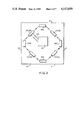
- FIG. 1 shows cells on a wafer.
- FIG. 2 shows the component parts of an individual cell of the first type.
- FIG. 3 shows the component parts of an individual cell of the second type.
- FIG. 4A shows the first manner of coupling of the link sections on opposite sides of a boundary.
- FIG. 4B shows the second manner of coupling of the link sections on opposite sides of a boundary.
- FIG. 5 shows how coupling between cells would be achieved in an array of cells where, contrary to the present invention, there is only one type of cell in the array of cells.
- FIG. 6 shows the disposition of the first and second types of cells on the wafer to achieve the configuration of the present invention.
- FIG. 1 shows a wafer-scale integrated circuit of a type suitable for the application thereto of the present invention.
- a wafer-scale integrated circuit 10 comprises a circular, semiconductor wafer 12 whereon are constructed a plurality of data processing cells 14.
- the cells 14 are square and form a regular tessellation across the surface of the wafer 12 such that each cell 14 shares common boundaries with four other cells 14.
- One of the cells 14 is omitted from the tessellation to provide a coupling port 16 whereby connection can be made from the outside world to the integrated circuit 10.
- the port 16 allows for coupling to the cells 14 immediately adjacent thereto for the transfer of data and commands and further allows for the provision of power and any common signals to all of the cells 14 simultaneously.
- the port 16 is shown as being central on the wafer 12. It is to be appreciated that the port 16 need not be central on the wafer 12, that there can be more than one port 16, and that the one or more ports 16 can be other than by the omission of a cell 14 from the tessellation. All that is required from the point of view of the present invention is that a method of providing data across one boundary of one cell 14 on the wafer 12 is available.
- FIG. 2 shows, in schematic form, the various constituent parts of a cell 14 according to the present invention and of the first of two types.
- the cell 14 has a Northern boundary N, a Southern boundary S, an Eastern boundary E and a Western boundary W.
- Each boundary N, S, E, W has associated therewith a link section 18N, 18S, 18E, 18W respectively, the letter suffix being indicative of the particular boundary N, S, E or W the link section 18 is associated.
- Unidirectional coupling sections 20NE, 20ES, 20SW and 20WN join the link sections 18N, 18S, 18E and 18W for the flow of data, the first letter of the two letter suffix being indicative of the link section 18 from which data is received and the second letter of the two letter suffix being indicative of the link section 18 to which a coupling section 20 delivers data.
- the first coupling section 20NE receives data from the Northern link section 18N and provides data to the Eastern link section 18E.
- the second coupling section 20ES receives data from the Eastern link section 18E and provides data to the Southern link section 18S.
- the third coupling section 20SW receives data from the Southern link section 18S and provides data to the Western link section 18W.
- the fourth coupling section 20WN receives data from the Western link section 18W and provides data to the Northern link section 18N.
- the link sections 18 are each individually and selectably operable to operate in a first mode where they couple data round the cell 14 and in a second mode where they couple data into and out of the cell 14 across their individual boundaries N, S, E, or W.
- the cell 14 also comprises a data processing element in the form of a memory module 22.
- the module 22 is provided with a bidirectional coupling 24 to the fourth coupling section 20WN.
- the module 22 receives commands with respect to its operation and data for its use via the fourth coupling section 20WN and delivers up to the fourth coupling section 20WN data it has operated on and any commands to be passed on to other modules 22 in other cells 14.
- the fourth coupling section 20WN then provides the output from the module 22 as the input to the Northern link section 18N.
- the module 22 can be serial or parallel receipt of signals passing through the coupling section 20WN.
- the module 22 can even be in series with the coupling section 20WN.
- the module 22 can receive its data down one or more lines and provide its output via one or more lines.
- the coupling sections 20NE, 20ES, 20SW and 20WN can range from a simple direct conductor connection to serial-in serial-out shift registers. All that is required of them is that they deliver what was received at their input to their output at some predictable later time.
- the three coupling sections 20NE, 20ES and 20SW not associated with the module 22 need to have the same time delay from input receipt to output presentation. It really does not matter about the delay of the coupling section 20WN associated with the module 22. Its delay can be of any acceptable length.
- FIG. 2 shows, in schematic outline, the various elements of the second kind of cell according to the present invention.
- the second kind of cell 14X is identical in every way with the first kind of cell 14 with the exception that the module 22, instead of being associated with the fourth coupling section 20WN, is associated with the second coupling section 20ES.
- the exact delay of the second coupling section 20ES then becomes unimportant in the second type of cell 14X provided it is the same as the delay of the fourth coupling section 20WN in the first type of cell 14.
- the delays of the remaining three coupling sections 20SW, 20WN and 20NE are the same as one another and the same as the delays in the remaining three coupling sections 20NE, 20ES, and 20SW in the first type of cell 14.
- FIG. 4A shows the manner of operation of the link sections 18 in adjacent cells across a boundary, and is particularly illustrative of the first mode of operation mentioned above.
- the Southern boundary S of a first cell 14 abuts onto the Northern boundary N of a second cell 14', the apostrophe suffix in the designation of an item being indicative of that item belonging to the second cell 14'.
- the Southern link section 18S of the first cell 14 receives data from the second coupling section 20ES of the first cell 14 and provides data as the input to the third coupling section 20SW of the first cell 14.
- the Northern link section 18N' of the second cell 14' receives data from the output of the fourth coupling section 20WN' of the second cell 14' and provides data to the input of the first coupling section 20NE' of the second cell 14'.
- the link sections 18S, 18N' are selectably operable to enter a first mode where each activates an internal through-coupling 24S, 24N' respectively.
- the output of the second coupling section 20ES of the first cell 14 is thereby routed via the internal through-coupling 24S in the Southern link section 18S of the first cell 14 to become the input to the third coupling section 20SW of the first cell 14 and the output of the fourth coupling section 20WN' of the second cell 14' is thereby routed via the internal through-coupling 24N' in the Northern link section 18N' of the second cell 14' to become the input to the first coupling section 20NE' of the second cell 14'.
- no data is transferred across the boundary S, N' between the link sections 18S, 18N'.
- FIG. 4B shows the manner of operation of the link sections 18 in adjacent cells 14 and is particularly illustrative of the second mode of operation of the link sections 18 as mentioned above.
- the Southern link section 18S of the first cell 14 and the Northern link section 18N' of the second cell 14' are both placed into a second mode of operation they co-operate to transfer data across the boundary S, N'.
- the Southern link section 18S of the first cell 14 provides the output of the second coupling section 20ES of the first cell 14 onto a Southern data output line 26S.
- the Northern link section 18N' of the second cell 14' provides the output of the fourth coupling section 20WN' of the second cell 14' as the signal on a Northern data output line 26N' of the second cell 14'.
- the Southern link section 18S of the first cell 14 accepts data from a Southern data input line 28S and couples it as the input to the third coupling section 20SW of the first cell 14.
- the Northern link section 18N' of the second cell 14' accepts the signal from a Northern data input line 28N' and couples it as the input to the first coupling section 20NE' of the second cell 14'.
- N' the Southern data output line 26S of the first cell 14 becomes the Northern data input line 28N' of the second cell 14' and the Northern data output line 26N' of the second cell 14' becomes the Southern data input line 28S of the first cell.
- the two link sections 18S, 18N' co-operate to provide the output of the second coupling section 20ES of the first cell 14 as the input to the first coupling section 20NE' of the second cell 14' and to provide the output of the fourth coupling section 20WN' of the second cell 14' as the input to the third coupling section 20SW of the first cell 14.
- U.S. Pat No. 4,471,483 issued 9/11/1984 describes the design and use of link section and coupling section used in the present invention, and how instruction may be transferred to each cell from a controller.
- U.S. Pat. No. 4,489,397 issued 12/18/84 teaches how a signal may be linked across a boundary and how instruction may be sent to a cell causing it to link to an adjacent cell.
- FIG. 5 shows how coupling would be achieved in an array of cells 14 where there is only one kind of cell 14, the coupling therefore not being according to the present invention.
- a portion 30 of the total number of cells 14 on the wafer 12 is shown.
- all of the cells 14 are of the first type as illustrated in FIG. 2.
- the Module 22 is therefore associated with the fourth coupling section 20WN. This association is symbolized by the module symbol 32 shown in the North-Western corner of each cell 14.
- the coupling sections 20 are illustrated by a data path 34 shown in solid line which passes round all incorporated cells 14 once unidirectionally, crossing the boundary between cells 14 wherever two adjacent link sections 18 co-operate to produce inter-cell coupling, and starting and finishing at a start cell 14"; which might be adjacent to the port 16 or might just be any cell 14 at any stage in the growth of an array of cells 14 on the wafer 12.
- the cells 14 which have been individually accessed from neighboring cells 14 and tested according to any convenient method, are incorporated into the array of cells 14 if they pass the test.
- the arrows 36 are illustrative of one possible order for their having been accessed, tested and incorporated, showing the approach made from neighboring cells 14.
- the array consists purely in cells of one type, in this case of the first type, the number of coupling sections 20 and link sections 18 encountered between successive modules 32 in the data path 34 is not constant.
- the distance between a first exemplary module 32A and a second exemplary module 32B, ignoring the particular coupling sections 20WN with which they are associated, is two link sections 18 and one coupling section 20, whereas the distance between a third exemplary module 32C and a fourth exemplary module 32D, once more ignoring the coupling section 20WN with which they are associated, is eight link sections 18 and seven coupling sections 20. This difference in distance can be taken to extremes and it is indeed possible to traverse the entire width of the wafer 12 on the data path 34 without encountering a module 32.
- FIG. 6 shows how coupling is achieved in an integrated circuit 10 comprising cells 14 of both the first type 14 and second type 14X and therefore being in accordance with the present invention.
- the same portion 30 of the cells 14 on the wafer 12 as was shown in FIG. 5 is shown in FIG. 6. Everything is the same in FIG. 6 as in FIG. 5, with the exception that the portion 30 of the body of cells 14 in FIG. 6 consists in cells of the first type 14 and cells of the second type 14X.
- the cells of the first type 14 and the cells of the second type 14X are alternated across the surface of the integrated circuit 10.
- the first fletched arrow 38 points along a diagonal row of cells of the first type 14 where the module 32 is associated with the fourth coupling section 20WN.
- the second fletched arrow 40 points along a diagonal row of cells of the second type 14X where the module 32 is associated with the second coupling section 20ES.
- the cells of the first type 14 alternate with the cells of the second type 14X in the same way that the black and white squares alternate on a chess board, alternate diagonal rows being of the first and second types of cells 14, 14X.
- no cell of the first type 14 shares a boundary N, S, E or W with any other cell of the first type 14, being entirely surrounded on its boundaries N, S, E, W by cells of the second type 14X.
- no cell of the second type 14X shares a common boundary N, S, E or W with any other cell of the second type 14X, being entirely surrounded on its boundaries N, S, E and W by cells of the first type 14.
Abstract
Description
Claims (7)
Applications Claiming Priority (2)
| Application Number | Priority Date | Filing Date | Title |
|---|---|---|---|
| GB8137017 | 1981-12-08 | ||
| GB8137017 | 1981-12-08 |
Publications (1)
| Publication Number | Publication Date |
|---|---|
| US4517659A true US4517659A (en) | 1985-05-14 |
Family
ID=10526461
Family Applications (1)
| Application Number | Title | Priority Date | Filing Date |
|---|---|---|---|
| US06/447,832 Expired - Fee Related US4517659A (en) | 1981-12-08 | 1982-12-08 | Constant-distance structure polycellular very large scale integrated circuit |
Country Status (5)
| Country | Link |
|---|---|
| US (1) | US4517659A (en) |
| EP (1) | EP0081309B1 (en) |
| JP (1) | JPS58110054A (en) |
| DE (1) | DE3279328D1 (en) |
| GB (1) | GB2111267B (en) |
Cited By (17)
| Publication number | Priority date | Publication date | Assignee | Title |
|---|---|---|---|---|
| US4656592A (en) * | 1983-10-14 | 1987-04-07 | U.S. Philips Corporation | Very large scale integrated circuit subdivided into isochronous regions, method for the machine-aided design of such a circuit, and method for the machine-aided testing of such a circuit |
| US4769644A (en) * | 1986-05-05 | 1988-09-06 | Texas Instruments Incorporated | Cellular automata devices |
| US4809346A (en) * | 1986-07-18 | 1989-02-28 | Hughes Aircraft Company | Computer vision architecture for iconic to symbolic transformation |
| US4847615A (en) * | 1985-10-14 | 1989-07-11 | Anamartic Limited | Control system for chained circuit modules |
| US5203005A (en) * | 1989-05-02 | 1993-04-13 | Horst Robert W | Cell structure for linear array wafer scale integration architecture with capability to open boundary i/o bus without neighbor acknowledgement |
| US5276893A (en) * | 1989-02-08 | 1994-01-04 | Yvon Savaria | Parallel microprocessor architecture |
| US5317755A (en) * | 1991-04-10 | 1994-05-31 | General Electric Company | Systolic array processors for reducing under-utilization of original design parallel-bit processors with digit-serial processors by using maximum common divisor of latency around the loop connection |
| US5349219A (en) * | 1989-06-15 | 1994-09-20 | Fujitsu Limited | Wafer-scale semiconductor integrated circuit device and method of forming interconnection lines arranged between chips of wafer-scale semiconductor integrated circuit device |
| US5379440A (en) * | 1990-12-20 | 1995-01-03 | Motorola Inc. | Parallel processor with array of clustered processing elements having inputs seperate from outputs and outputs limited to a maximum of two per dimension |
| US5421019A (en) * | 1988-10-07 | 1995-05-30 | Martin Marietta Corporation | Parallel data processor |
| WO1996014662A1 (en) * | 1994-11-02 | 1996-05-17 | Lsi Logic Corporation | Microelectronic integrated circuit structure and method using three directional interconnect routing based on hexagonal geometry |
| US5990488A (en) * | 1999-01-04 | 1999-11-23 | Advanced Micro Devices, Inc. | Useable drop-in strategy for correct electrical analysis of semiconductor devices |
| US6067609A (en) * | 1998-04-09 | 2000-05-23 | Teranex, Inc. | Pattern generation and shift plane operations for a mesh connected computer |
| US6073185A (en) * | 1993-08-27 | 2000-06-06 | Teranex, Inc. | Parallel data processor |
| US6173388B1 (en) | 1998-04-09 | 2001-01-09 | Teranex Inc. | Directly accessing local memories of array processors for improved real-time corner turning processing |
| US6185667B1 (en) | 1998-04-09 | 2001-02-06 | Teranex, Inc. | Input/output support for processing in a mesh connected computer |
| US6212628B1 (en) | 1998-04-09 | 2001-04-03 | Teranex, Inc. | Mesh connected computer |
Families Citing this family (1)
| Publication number | Priority date | Publication date | Assignee | Title |
|---|---|---|---|---|
| GB2174518B (en) * | 1985-04-15 | 1989-06-21 | Sinclair Res Ltd | Wafer scale integrated circuit |
Citations (6)
| Publication number | Priority date | Publication date | Assignee | Title |
|---|---|---|---|---|
| US3106698A (en) * | 1958-04-25 | 1963-10-08 | Bell Telephone Labor Inc | Parallel data processing apparatus |
| US3794983A (en) * | 1973-04-17 | 1974-02-26 | K Sahin | Communication method and network system |
| US4060713A (en) * | 1971-06-23 | 1977-11-29 | The Perkin-Elmer Corporation | Analysis of images |
| US4065808A (en) * | 1975-01-25 | 1977-12-27 | U.S. Philips Corporation | Network computer system |
| US4192004A (en) * | 1977-09-08 | 1980-03-04 | Buerger Walter R | Topological transformation system |
| US4215401A (en) * | 1978-09-28 | 1980-07-29 | Environmental Research Institute Of Michigan | Cellular digital array processor |
Family Cites Families (2)
| Publication number | Priority date | Publication date | Assignee | Title |
|---|---|---|---|---|
| GB1377859A (en) * | 1972-08-03 | 1974-12-18 | Catt I | Digital integrated circuits |
| GB2114782B (en) * | 1981-12-02 | 1985-06-05 | Burroughs Corp | Branched-spiral wafer-scale integrated circuit |
-
1982
- 1982-11-18 GB GB08232919A patent/GB2111267B/en not_active Expired
- 1982-11-18 EP EP82306143A patent/EP0081309B1/en not_active Expired
- 1982-11-18 DE DE8282306143T patent/DE3279328D1/en not_active Expired
- 1982-11-29 JP JP57210545A patent/JPS58110054A/en active Granted
- 1982-12-08 US US06/447,832 patent/US4517659A/en not_active Expired - Fee Related
Patent Citations (6)
| Publication number | Priority date | Publication date | Assignee | Title |
|---|---|---|---|---|
| US3106698A (en) * | 1958-04-25 | 1963-10-08 | Bell Telephone Labor Inc | Parallel data processing apparatus |
| US4060713A (en) * | 1971-06-23 | 1977-11-29 | The Perkin-Elmer Corporation | Analysis of images |
| US3794983A (en) * | 1973-04-17 | 1974-02-26 | K Sahin | Communication method and network system |
| US4065808A (en) * | 1975-01-25 | 1977-12-27 | U.S. Philips Corporation | Network computer system |
| US4192004A (en) * | 1977-09-08 | 1980-03-04 | Buerger Walter R | Topological transformation system |
| US4215401A (en) * | 1978-09-28 | 1980-07-29 | Environmental Research Institute Of Michigan | Cellular digital array processor |
Cited By (20)
| Publication number | Priority date | Publication date | Assignee | Title |
|---|---|---|---|---|
| US4656592A (en) * | 1983-10-14 | 1987-04-07 | U.S. Philips Corporation | Very large scale integrated circuit subdivided into isochronous regions, method for the machine-aided design of such a circuit, and method for the machine-aided testing of such a circuit |
| US4847615A (en) * | 1985-10-14 | 1989-07-11 | Anamartic Limited | Control system for chained circuit modules |
| US4769644A (en) * | 1986-05-05 | 1988-09-06 | Texas Instruments Incorporated | Cellular automata devices |
| US4809346A (en) * | 1986-07-18 | 1989-02-28 | Hughes Aircraft Company | Computer vision architecture for iconic to symbolic transformation |
| US5421019A (en) * | 1988-10-07 | 1995-05-30 | Martin Marietta Corporation | Parallel data processor |
| US5276893A (en) * | 1989-02-08 | 1994-01-04 | Yvon Savaria | Parallel microprocessor architecture |
| US5287472A (en) * | 1989-05-02 | 1994-02-15 | Tandem Computers Incorporated | Memory system using linear array wafer scale integration architecture |
| US5203005A (en) * | 1989-05-02 | 1993-04-13 | Horst Robert W | Cell structure for linear array wafer scale integration architecture with capability to open boundary i/o bus without neighbor acknowledgement |
| US5349219A (en) * | 1989-06-15 | 1994-09-20 | Fujitsu Limited | Wafer-scale semiconductor integrated circuit device and method of forming interconnection lines arranged between chips of wafer-scale semiconductor integrated circuit device |
| US5379440A (en) * | 1990-12-20 | 1995-01-03 | Motorola Inc. | Parallel processor with array of clustered processing elements having inputs seperate from outputs and outputs limited to a maximum of two per dimension |
| US5317755A (en) * | 1991-04-10 | 1994-05-31 | General Electric Company | Systolic array processors for reducing under-utilization of original design parallel-bit processors with digit-serial processors by using maximum common divisor of latency around the loop connection |
| US6073185A (en) * | 1993-08-27 | 2000-06-06 | Teranex, Inc. | Parallel data processor |
| US5578840A (en) * | 1994-11-02 | 1996-11-26 | Lis Logic Corporation | Microelectronic integrated circuit structure and method using three directional interconnect routing based on hexagonal geometry |
| WO1996014662A1 (en) * | 1994-11-02 | 1996-05-17 | Lsi Logic Corporation | Microelectronic integrated circuit structure and method using three directional interconnect routing based on hexagonal geometry |
| US6067609A (en) * | 1998-04-09 | 2000-05-23 | Teranex, Inc. | Pattern generation and shift plane operations for a mesh connected computer |
| US6173388B1 (en) | 1998-04-09 | 2001-01-09 | Teranex Inc. | Directly accessing local memories of array processors for improved real-time corner turning processing |
| US6185667B1 (en) | 1998-04-09 | 2001-02-06 | Teranex, Inc. | Input/output support for processing in a mesh connected computer |
| US6212628B1 (en) | 1998-04-09 | 2001-04-03 | Teranex, Inc. | Mesh connected computer |
| US6275920B1 (en) | 1998-04-09 | 2001-08-14 | Teranex, Inc. | Mesh connected computed |
| US5990488A (en) * | 1999-01-04 | 1999-11-23 | Advanced Micro Devices, Inc. | Useable drop-in strategy for correct electrical analysis of semiconductor devices |
Also Published As
| Publication number | Publication date |
|---|---|
| EP0081309A2 (en) | 1983-06-15 |
| DE3279328D1 (en) | 1989-02-09 |
| JPS58110054A (en) | 1983-06-30 |
| EP0081309B1 (en) | 1989-01-04 |
| GB2111267A (en) | 1983-06-29 |
| JPH0236069B2 (en) | 1990-08-15 |
| GB2111267B (en) | 1985-10-16 |
| EP0081309A3 (en) | 1985-12-18 |
Similar Documents
| Publication | Publication Date | Title |
|---|---|---|
| US4517659A (en) | Constant-distance structure polycellular very large scale integrated circuit | |
| KR100202131B1 (en) | Programmable logic cell and array | |
| EP0256661B1 (en) | Array processor | |
| US4467422A (en) | Array processor | |
| US5260610A (en) | Programmable logic element interconnections for programmable logic array integrated circuits | |
| EP0490511B1 (en) | Nonvolatile serially programmable devices | |
| JPS5833977B2 (en) | array processor | |
| US5204556A (en) | Programmable interconnect structure for logic blocks | |
| CN100403445C (en) | MRAM with midpoint generator reference | |
| US5734869A (en) | High speed logic circuit simulator | |
| US4509146A (en) | High density Josephson junction memory circuit | |
| US5070446A (en) | Method of simulating a hexagonal array of computer processors and/or memories | |
| EP0013290A1 (en) | Large scale integrated circuit wafer and method of testing same | |
| CA2116332A1 (en) | Programme logic cell and array | |
| EP0411069A1 (en) | Redundancy and testing techniques for ic wafers | |
| US6218859B1 (en) | Programmable logic device having quadrant layout | |
| US4471483A (en) | Branched labyrinth wafer-scale integrated circuit | |
| US10468386B1 (en) | TSV redundancy and TSV test select scheme | |
| EP0512536B1 (en) | Programmable logic unit circuit | |
| JP3158286B2 (en) | Multiport memory | |
| WO1986006186A1 (en) | Wafer scale integrated circuit | |
| JPH04288659A (en) | Processor array | |
| CA1239700A (en) | Expandable electronic matrix | |
| US3381282A (en) | Core matrix winding pattern | |
| EP0172311B1 (en) | Memory element for a wafer scale integrated circuit |
Legal Events
| Date | Code | Title | Description |
|---|---|---|---|
| AS | Assignment |
Owner name: BURROUGHS CORPORATION Free format text: MERGER;ASSIGNORS:BURROUGHS CORPORATION A CORP OF MI (MERGED INTO);BURROUGHS DELAWARE INCORPORATED A DE CORP. (CHANGED TO);REEL/FRAME:004312/0324 Effective date: 19840530 |
|
| AS | Assignment |
Owner name: BURROUGHS CORPORATION, DETROIT, MI, A CORP OF DE Free format text: ASSIGNMENT OF ASSIGNORS INTEREST.;ASSIGNOR:CHAMBERLAIN, JOHN T.;REEL/FRAME:004368/0791 Effective date: 19850125 |
|
| FPAY | Fee payment |
Year of fee payment: 4 |
|
| AS | Assignment |
Owner name: UNISYS CORPORATION, PENNSYLVANIA Free format text: MERGER;ASSIGNOR:BURROUGHS CORPORATION;REEL/FRAME:005012/0501 Effective date: 19880509 |
|
| FEPP | Fee payment procedure |
Free format text: PAYOR NUMBER ASSIGNED (ORIGINAL EVENT CODE: ASPN); ENTITY STATUS OF PATENT OWNER: LARGE ENTITY |
|
| FPAY | Fee payment |
Year of fee payment: 8 |
|
| REMI | Maintenance fee reminder mailed | ||
| LAPS | Lapse for failure to pay maintenance fees | ||
| FP | Lapsed due to failure to pay maintenance fee |
Effective date: 19970514 |
|
| STCH | Information on status: patent discontinuation |
Free format text: PATENT EXPIRED DUE TO NONPAYMENT OF MAINTENANCE FEES UNDER 37 CFR 1.362 |