US4505029A - Semiconductor device with built-up low resistance contact - Google Patents
Semiconductor device with built-up low resistance contact Download PDFInfo
- Publication number
- US4505029A US4505029A US06/501,745 US50174583A US4505029A US 4505029 A US4505029 A US 4505029A US 50174583 A US50174583 A US 50174583A US 4505029 A US4505029 A US 4505029A
- Authority
- US
- United States
- Prior art keywords
- layer
- forming
- solder
- metal
- contact
- Prior art date
- Legal status (The legal status is an assumption and is not a legal conclusion. Google has not performed a legal analysis and makes no representation as to the accuracy of the status listed.)
- Expired - Lifetime
Links
- 239000004065 semiconductor Substances 0.000 title claims abstract description 46
- 239000010410 layer Substances 0.000 claims description 179
- 239000000463 material Substances 0.000 claims description 41
- 229910052751 metal Inorganic materials 0.000 claims description 33
- 239000002184 metal Substances 0.000 claims description 33
- 238000000034 method Methods 0.000 claims description 30
- 229910000679 solder Inorganic materials 0.000 claims description 26
- 230000004888 barrier function Effects 0.000 claims description 14
- 239000003989 dielectric material Substances 0.000 claims description 10
- 238000005530 etching Methods 0.000 claims description 7
- 230000000873 masking effect Effects 0.000 claims description 6
- 239000011241 protective layer Substances 0.000 claims description 4
- 238000010438 heat treatment Methods 0.000 claims description 3
- 238000007747 plating Methods 0.000 claims description 3
- 229910045601 alloy Inorganic materials 0.000 claims description 2
- 239000000956 alloy Substances 0.000 claims description 2
- 238000004544 sputter deposition Methods 0.000 claims description 2
- 239000002355 dual-layer Substances 0.000 claims 2
- 230000001681 protective effect Effects 0.000 claims 2
- 238000001465 metallisation Methods 0.000 description 20
- 239000004642 Polyimide Substances 0.000 description 16
- 229920001721 polyimide Polymers 0.000 description 16
- RYGMFSIKBFXOCR-UHFFFAOYSA-N Copper Chemical compound [Cu] RYGMFSIKBFXOCR-UHFFFAOYSA-N 0.000 description 15
- 229910052802 copper Inorganic materials 0.000 description 15
- 239000010949 copper Substances 0.000 description 15
- 235000012431 wafers Nutrition 0.000 description 11
- 229910052782 aluminium Inorganic materials 0.000 description 10
- XAGFODPZIPBFFR-UHFFFAOYSA-N aluminium Chemical compound [Al] XAGFODPZIPBFFR-UHFFFAOYSA-N 0.000 description 10
- 230000015572 biosynthetic process Effects 0.000 description 9
- 229920002120 photoresistant polymer Polymers 0.000 description 9
- VYZAMTAEIAYCRO-UHFFFAOYSA-N Chromium Chemical compound [Cr] VYZAMTAEIAYCRO-UHFFFAOYSA-N 0.000 description 7
- 229910021420 polycrystalline silicon Inorganic materials 0.000 description 7
- 229920005591 polysilicon Polymers 0.000 description 7
- PXHVJJICTQNCMI-UHFFFAOYSA-N Nickel Chemical compound [Ni] PXHVJJICTQNCMI-UHFFFAOYSA-N 0.000 description 6
- RTAQQCXQSZGOHL-UHFFFAOYSA-N Titanium Chemical compound [Ti] RTAQQCXQSZGOHL-UHFFFAOYSA-N 0.000 description 6
- 229910052804 chromium Inorganic materials 0.000 description 6
- 239000011651 chromium Substances 0.000 description 6
- 229910052719 titanium Inorganic materials 0.000 description 6
- 239000010936 titanium Substances 0.000 description 6
- QVGXLLKOCUKJST-UHFFFAOYSA-N atomic oxygen Chemical compound [O] QVGXLLKOCUKJST-UHFFFAOYSA-N 0.000 description 5
- LQBJWKCYZGMFEV-UHFFFAOYSA-N lead tin Chemical compound [Sn].[Pb] LQBJWKCYZGMFEV-UHFFFAOYSA-N 0.000 description 5
- 238000004519 manufacturing process Methods 0.000 description 5
- 239000001301 oxygen Substances 0.000 description 5
- 229910052760 oxygen Inorganic materials 0.000 description 5
- 230000008569 process Effects 0.000 description 5
- 239000000758 substrate Substances 0.000 description 5
- ATJFFYVFTNAWJD-UHFFFAOYSA-N Tin Chemical compound [Sn] ATJFFYVFTNAWJD-UHFFFAOYSA-N 0.000 description 4
- BQCADISMDOOEFD-UHFFFAOYSA-N Silver Chemical compound [Ag] BQCADISMDOOEFD-UHFFFAOYSA-N 0.000 description 3
- 239000008367 deionised water Substances 0.000 description 3
- 229910021641 deionized water Inorganic materials 0.000 description 3
- 229910052759 nickel Inorganic materials 0.000 description 3
- 239000010956 nickel silver Substances 0.000 description 3
- 238000000059 patterning Methods 0.000 description 3
- 238000001020 plasma etching Methods 0.000 description 3
- 229910052709 silver Inorganic materials 0.000 description 3
- 239000004332 silver Substances 0.000 description 3
- XLYOFNOQVPJJNP-UHFFFAOYSA-N water Chemical compound O XLYOFNOQVPJJNP-UHFFFAOYSA-N 0.000 description 3
- CSCPPACGZOOCGX-UHFFFAOYSA-N Acetone Chemical compound CC(C)=O CSCPPACGZOOCGX-UHFFFAOYSA-N 0.000 description 2
- IJGRMHOSHXDMSA-UHFFFAOYSA-N Atomic nitrogen Chemical compound N#N IJGRMHOSHXDMSA-UHFFFAOYSA-N 0.000 description 2
- VEXZGXHMUGYJMC-UHFFFAOYSA-N Hydrochloric acid Chemical compound Cl VEXZGXHMUGYJMC-UHFFFAOYSA-N 0.000 description 2
- VYPSYNLAJGMNEJ-UHFFFAOYSA-N Silicium dioxide Chemical compound O=[Si]=O VYPSYNLAJGMNEJ-UHFFFAOYSA-N 0.000 description 2
- 229910001128 Sn alloy Inorganic materials 0.000 description 2
- 238000000576 coating method Methods 0.000 description 2
- 238000007796 conventional method Methods 0.000 description 2
- 238000009826 distribution Methods 0.000 description 2
- UFHFLCQGNIYNRP-UHFFFAOYSA-N Hydrogen Chemical compound [H][H] UFHFLCQGNIYNRP-UHFFFAOYSA-N 0.000 description 1
- QAOWNCQODCNURD-UHFFFAOYSA-N Sulfuric acid Chemical compound OS(O)(=O)=O QAOWNCQODCNURD-UHFFFAOYSA-N 0.000 description 1
- 239000002253 acid Substances 0.000 description 1
- 238000000637 aluminium metallisation Methods 0.000 description 1
- 230000015556 catabolic process Effects 0.000 description 1
- 238000004140 cleaning Methods 0.000 description 1
- 239000011248 coating agent Substances 0.000 description 1
- 238000010276 construction Methods 0.000 description 1
- 230000003247 decreasing effect Effects 0.000 description 1
- 238000006731 degradation reaction Methods 0.000 description 1
- 238000000151 deposition Methods 0.000 description 1
- 230000008021 deposition Effects 0.000 description 1
- KPUWHANPEXNPJT-UHFFFAOYSA-N disiloxane Chemical class [SiH3]O[SiH3] KPUWHANPEXNPJT-UHFFFAOYSA-N 0.000 description 1
- 230000000694 effects Effects 0.000 description 1
- 238000005566 electron beam evaporation Methods 0.000 description 1
- 230000002708 enhancing effect Effects 0.000 description 1
- 230000001747 exhibiting effect Effects 0.000 description 1
- 230000005669 field effect Effects 0.000 description 1
- PCHJSUWPFVWCPO-UHFFFAOYSA-N gold Chemical compound [Au] PCHJSUWPFVWCPO-UHFFFAOYSA-N 0.000 description 1
- 229910052737 gold Inorganic materials 0.000 description 1
- 239000010931 gold Substances 0.000 description 1
- 239000001257 hydrogen Substances 0.000 description 1
- 229910052739 hydrogen Inorganic materials 0.000 description 1
- 230000003993 interaction Effects 0.000 description 1
- 238000005304 joining Methods 0.000 description 1
- 238000012986 modification Methods 0.000 description 1
- 230000004048 modification Effects 0.000 description 1
- 229910052757 nitrogen Inorganic materials 0.000 description 1
- NJPPVKZQTLUDBO-UHFFFAOYSA-N novaluron Chemical compound C1=C(Cl)C(OC(F)(F)C(OC(F)(F)F)F)=CC=C1NC(=O)NC(=O)C1=C(F)C=CC=C1F NJPPVKZQTLUDBO-UHFFFAOYSA-N 0.000 description 1
- 230000008520 organization Effects 0.000 description 1
- 230000003647 oxidation Effects 0.000 description 1
- 238000007254 oxidation reaction Methods 0.000 description 1
- 229920001296 polysiloxane Polymers 0.000 description 1
- 230000002028 premature Effects 0.000 description 1
- 238000011112 process operation Methods 0.000 description 1
- 230000004044 response Effects 0.000 description 1
- 229910052710 silicon Inorganic materials 0.000 description 1
- 239000010703 silicon Substances 0.000 description 1
- 239000000377 silicon dioxide Substances 0.000 description 1
- 235000012239 silicon dioxide Nutrition 0.000 description 1
- 239000002356 single layer Substances 0.000 description 1
- 238000005476 soldering Methods 0.000 description 1
- 238000009987 spinning Methods 0.000 description 1
- 238000000992 sputter etching Methods 0.000 description 1
- 239000001117 sulphuric acid Substances 0.000 description 1
- 235000011149 sulphuric acid Nutrition 0.000 description 1
- 238000005382 thermal cycling Methods 0.000 description 1
Images

Classifications
-
- H—ELECTRICITY
- H01—ELECTRIC ELEMENTS
- H01L—SEMICONDUCTOR DEVICES NOT COVERED BY CLASS H10
- H01L23/00—Details of semiconductor or other solid state devices
- H01L23/48—Arrangements for conducting electric current to or from the solid state body in operation, e.g. leads, terminal arrangements ; Selection of materials therefor
- H01L23/482—Arrangements for conducting electric current to or from the solid state body in operation, e.g. leads, terminal arrangements ; Selection of materials therefor consisting of lead-in layers inseparably applied to the semiconductor body
- H01L23/4824—Pads with extended contours, e.g. grid structure, branch structure, finger structure
-
- H—ELECTRICITY
- H01—ELECTRIC ELEMENTS
- H01L—SEMICONDUCTOR DEVICES NOT COVERED BY CLASS H10
- H01L24/00—Arrangements for connecting or disconnecting semiconductor or solid-state bodies; Methods or apparatus related thereto
- H01L24/01—Means for bonding being attached to, or being formed on, the surface to be connected, e.g. chip-to-package, die-attach, "first-level" interconnects; Manufacturing methods related thereto
- H01L24/10—Bump connectors ; Manufacturing methods related thereto
- H01L24/12—Structure, shape, material or disposition of the bump connectors prior to the connecting process
- H01L24/13—Structure, shape, material or disposition of the bump connectors prior to the connecting process of an individual bump connector
-
- H—ELECTRICITY
- H01—ELECTRIC ELEMENTS
- H01L—SEMICONDUCTOR DEVICES NOT COVERED BY CLASS H10
- H01L23/00—Details of semiconductor or other solid state devices
- H01L23/48—Arrangements for conducting electric current to or from the solid state body in operation, e.g. leads, terminal arrangements ; Selection of materials therefor
- H01L23/482—Arrangements for conducting electric current to or from the solid state body in operation, e.g. leads, terminal arrangements ; Selection of materials therefor consisting of lead-in layers inseparably applied to the semiconductor body
- H01L23/485—Arrangements for conducting electric current to or from the solid state body in operation, e.g. leads, terminal arrangements ; Selection of materials therefor consisting of lead-in layers inseparably applied to the semiconductor body consisting of layered constructions comprising conductive layers and insulating layers, e.g. planar contacts
-
- H—ELECTRICITY
- H01—ELECTRIC ELEMENTS
- H01L—SEMICONDUCTOR DEVICES NOT COVERED BY CLASS H10
- H01L24/00—Arrangements for connecting or disconnecting semiconductor or solid-state bodies; Methods or apparatus related thereto
- H01L24/01—Means for bonding being attached to, or being formed on, the surface to be connected, e.g. chip-to-package, die-attach, "first-level" interconnects; Manufacturing methods related thereto
- H01L24/02—Bonding areas ; Manufacturing methods related thereto
- H01L24/03—Manufacturing methods
-
- H—ELECTRICITY
- H01—ELECTRIC ELEMENTS
- H01L—SEMICONDUCTOR DEVICES NOT COVERED BY CLASS H10
- H01L24/00—Arrangements for connecting or disconnecting semiconductor or solid-state bodies; Methods or apparatus related thereto
- H01L24/01—Means for bonding being attached to, or being formed on, the surface to be connected, e.g. chip-to-package, die-attach, "first-level" interconnects; Manufacturing methods related thereto
- H01L24/02—Bonding areas ; Manufacturing methods related thereto
- H01L24/04—Structure, shape, material or disposition of the bonding areas prior to the connecting process
- H01L24/05—Structure, shape, material or disposition of the bonding areas prior to the connecting process of an individual bonding area
-
- H—ELECTRICITY
- H01—ELECTRIC ELEMENTS
- H01L—SEMICONDUCTOR DEVICES NOT COVERED BY CLASS H10
- H01L2224/00—Indexing scheme for arrangements for connecting or disconnecting semiconductor or solid-state bodies and methods related thereto as covered by H01L24/00
- H01L2224/01—Means for bonding being attached to, or being formed on, the surface to be connected, e.g. chip-to-package, die-attach, "first-level" interconnects; Manufacturing methods related thereto
- H01L2224/02—Bonding areas; Manufacturing methods related thereto
- H01L2224/04—Structure, shape, material or disposition of the bonding areas prior to the connecting process
- H01L2224/05—Structure, shape, material or disposition of the bonding areas prior to the connecting process of an individual bonding area
- H01L2224/05001—Internal layers
- H01L2224/05099—Material
- H01L2224/051—Material with a principal constituent of the material being a metal or a metalloid, e.g. boron [B], silicon [Si], germanium [Ge], arsenic [As], antimony [Sb], tellurium [Te] and polonium [Po], and alloys thereof
- H01L2224/05117—Material with a principal constituent of the material being a metal or a metalloid, e.g. boron [B], silicon [Si], germanium [Ge], arsenic [As], antimony [Sb], tellurium [Te] and polonium [Po], and alloys thereof the principal constituent melting at a temperature of greater than or equal to 400°C and less than 950°C
- H01L2224/05124—Aluminium [Al] as principal constituent
-
- H—ELECTRICITY
- H01—ELECTRIC ELEMENTS
- H01L—SEMICONDUCTOR DEVICES NOT COVERED BY CLASS H10
- H01L2224/00—Indexing scheme for arrangements for connecting or disconnecting semiconductor or solid-state bodies and methods related thereto as covered by H01L24/00
- H01L2224/01—Means for bonding being attached to, or being formed on, the surface to be connected, e.g. chip-to-package, die-attach, "first-level" interconnects; Manufacturing methods related thereto
- H01L2224/02—Bonding areas; Manufacturing methods related thereto
- H01L2224/04—Structure, shape, material or disposition of the bonding areas prior to the connecting process
- H01L2224/05—Structure, shape, material or disposition of the bonding areas prior to the connecting process of an individual bonding area
- H01L2224/05001—Internal layers
- H01L2224/05099—Material
- H01L2224/051—Material with a principal constituent of the material being a metal or a metalloid, e.g. boron [B], silicon [Si], germanium [Ge], arsenic [As], antimony [Sb], tellurium [Te] and polonium [Po], and alloys thereof
- H01L2224/05138—Material with a principal constituent of the material being a metal or a metalloid, e.g. boron [B], silicon [Si], germanium [Ge], arsenic [As], antimony [Sb], tellurium [Te] and polonium [Po], and alloys thereof the principal constituent melting at a temperature of greater than or equal to 950°C and less than 1550°C
- H01L2224/05147—Copper [Cu] as principal constituent
-
- H—ELECTRICITY
- H01—ELECTRIC ELEMENTS
- H01L—SEMICONDUCTOR DEVICES NOT COVERED BY CLASS H10
- H01L2224/00—Indexing scheme for arrangements for connecting or disconnecting semiconductor or solid-state bodies and methods related thereto as covered by H01L24/00
- H01L2224/01—Means for bonding being attached to, or being formed on, the surface to be connected, e.g. chip-to-package, die-attach, "first-level" interconnects; Manufacturing methods related thereto
- H01L2224/02—Bonding areas; Manufacturing methods related thereto
- H01L2224/04—Structure, shape, material or disposition of the bonding areas prior to the connecting process
- H01L2224/05—Structure, shape, material or disposition of the bonding areas prior to the connecting process of an individual bonding area
- H01L2224/05001—Internal layers
- H01L2224/05099—Material
- H01L2224/051—Material with a principal constituent of the material being a metal or a metalloid, e.g. boron [B], silicon [Si], germanium [Ge], arsenic [As], antimony [Sb], tellurium [Te] and polonium [Po], and alloys thereof
- H01L2224/05163—Material with a principal constituent of the material being a metal or a metalloid, e.g. boron [B], silicon [Si], germanium [Ge], arsenic [As], antimony [Sb], tellurium [Te] and polonium [Po], and alloys thereof the principal constituent melting at a temperature of greater than 1550°C
- H01L2224/05171—Chromium [Cr] as principal constituent
-
- H—ELECTRICITY
- H01—ELECTRIC ELEMENTS
- H01L—SEMICONDUCTOR DEVICES NOT COVERED BY CLASS H10
- H01L2224/00—Indexing scheme for arrangements for connecting or disconnecting semiconductor or solid-state bodies and methods related thereto as covered by H01L24/00
- H01L2224/01—Means for bonding being attached to, or being formed on, the surface to be connected, e.g. chip-to-package, die-attach, "first-level" interconnects; Manufacturing methods related thereto
- H01L2224/02—Bonding areas; Manufacturing methods related thereto
- H01L2224/04—Structure, shape, material or disposition of the bonding areas prior to the connecting process
- H01L2224/05—Structure, shape, material or disposition of the bonding areas prior to the connecting process of an individual bonding area
- H01L2224/0554—External layer
- H01L2224/05599—Material
- H01L2224/056—Material with a principal constituent of the material being a metal or a metalloid, e.g. boron [B], silicon [Si], germanium [Ge], arsenic [As], antimony [Sb], tellurium [Te] and polonium [Po], and alloys thereof
- H01L2224/05638—Material with a principal constituent of the material being a metal or a metalloid, e.g. boron [B], silicon [Si], germanium [Ge], arsenic [As], antimony [Sb], tellurium [Te] and polonium [Po], and alloys thereof the principal constituent melting at a temperature of greater than or equal to 950°C and less than 1550°C
- H01L2224/05647—Copper [Cu] as principal constituent
-
- H—ELECTRICITY
- H01—ELECTRIC ELEMENTS
- H01L—SEMICONDUCTOR DEVICES NOT COVERED BY CLASS H10
- H01L2224/00—Indexing scheme for arrangements for connecting or disconnecting semiconductor or solid-state bodies and methods related thereto as covered by H01L24/00
- H01L2224/01—Means for bonding being attached to, or being formed on, the surface to be connected, e.g. chip-to-package, die-attach, "first-level" interconnects; Manufacturing methods related thereto
- H01L2224/10—Bump connectors; Manufacturing methods related thereto
- H01L2224/12—Structure, shape, material or disposition of the bump connectors prior to the connecting process
- H01L2224/13—Structure, shape, material or disposition of the bump connectors prior to the connecting process of an individual bump connector
- H01L2224/13001—Core members of the bump connector
- H01L2224/13099—Material
- H01L2224/131—Material with a principal constituent of the material being a metal or a metalloid, e.g. boron [B], silicon [Si], germanium [Ge], arsenic [As], antimony [Sb], tellurium [Te] and polonium [Po], and alloys thereof
- H01L2224/13101—Material with a principal constituent of the material being a metal or a metalloid, e.g. boron [B], silicon [Si], germanium [Ge], arsenic [As], antimony [Sb], tellurium [Te] and polonium [Po], and alloys thereof the principal constituent melting at a temperature of less than 400°C
- H01L2224/13116—Lead [Pb] as principal constituent
-
- H—ELECTRICITY
- H01—ELECTRIC ELEMENTS
- H01L—SEMICONDUCTOR DEVICES NOT COVERED BY CLASS H10
- H01L24/00—Arrangements for connecting or disconnecting semiconductor or solid-state bodies; Methods or apparatus related thereto
- H01L24/01—Means for bonding being attached to, or being formed on, the surface to be connected, e.g. chip-to-package, die-attach, "first-level" interconnects; Manufacturing methods related thereto
- H01L24/10—Bump connectors ; Manufacturing methods related thereto
- H01L24/11—Manufacturing methods
-
- H—ELECTRICITY
- H01—ELECTRIC ELEMENTS
- H01L—SEMICONDUCTOR DEVICES NOT COVERED BY CLASS H10
- H01L2924/00—Indexing scheme for arrangements or methods for connecting or disconnecting semiconductor or solid-state bodies as covered by H01L24/00
- H01L2924/0001—Technical content checked by a classifier
-
- H—ELECTRICITY
- H01—ELECTRIC ELEMENTS
- H01L—SEMICONDUCTOR DEVICES NOT COVERED BY CLASS H10
- H01L2924/00—Indexing scheme for arrangements or methods for connecting or disconnecting semiconductor or solid-state bodies as covered by H01L24/00
- H01L2924/01—Chemical elements
- H01L2924/01005—Boron [B]
-
- H—ELECTRICITY
- H01—ELECTRIC ELEMENTS
- H01L—SEMICONDUCTOR DEVICES NOT COVERED BY CLASS H10
- H01L2924/00—Indexing scheme for arrangements or methods for connecting or disconnecting semiconductor or solid-state bodies as covered by H01L24/00
- H01L2924/01—Chemical elements
- H01L2924/01006—Carbon [C]
-
- H—ELECTRICITY
- H01—ELECTRIC ELEMENTS
- H01L—SEMICONDUCTOR DEVICES NOT COVERED BY CLASS H10
- H01L2924/00—Indexing scheme for arrangements or methods for connecting or disconnecting semiconductor or solid-state bodies as covered by H01L24/00
- H01L2924/01—Chemical elements
- H01L2924/01013—Aluminum [Al]
-
- H—ELECTRICITY
- H01—ELECTRIC ELEMENTS
- H01L—SEMICONDUCTOR DEVICES NOT COVERED BY CLASS H10
- H01L2924/00—Indexing scheme for arrangements or methods for connecting or disconnecting semiconductor or solid-state bodies as covered by H01L24/00
- H01L2924/01—Chemical elements
- H01L2924/01015—Phosphorus [P]
-
- H—ELECTRICITY
- H01—ELECTRIC ELEMENTS
- H01L—SEMICONDUCTOR DEVICES NOT COVERED BY CLASS H10
- H01L2924/00—Indexing scheme for arrangements or methods for connecting or disconnecting semiconductor or solid-state bodies as covered by H01L24/00
- H01L2924/01—Chemical elements
- H01L2924/01022—Titanium [Ti]
-
- H—ELECTRICITY
- H01—ELECTRIC ELEMENTS
- H01L—SEMICONDUCTOR DEVICES NOT COVERED BY CLASS H10
- H01L2924/00—Indexing scheme for arrangements or methods for connecting or disconnecting semiconductor or solid-state bodies as covered by H01L24/00
- H01L2924/01—Chemical elements
- H01L2924/01024—Chromium [Cr]
-
- H—ELECTRICITY
- H01—ELECTRIC ELEMENTS
- H01L—SEMICONDUCTOR DEVICES NOT COVERED BY CLASS H10
- H01L2924/00—Indexing scheme for arrangements or methods for connecting or disconnecting semiconductor or solid-state bodies as covered by H01L24/00
- H01L2924/01—Chemical elements
- H01L2924/01029—Copper [Cu]
-
- H—ELECTRICITY
- H01—ELECTRIC ELEMENTS
- H01L—SEMICONDUCTOR DEVICES NOT COVERED BY CLASS H10
- H01L2924/00—Indexing scheme for arrangements or methods for connecting or disconnecting semiconductor or solid-state bodies as covered by H01L24/00
- H01L2924/01—Chemical elements
- H01L2924/01033—Arsenic [As]
-
- H—ELECTRICITY
- H01—ELECTRIC ELEMENTS
- H01L—SEMICONDUCTOR DEVICES NOT COVERED BY CLASS H10
- H01L2924/00—Indexing scheme for arrangements or methods for connecting or disconnecting semiconductor or solid-state bodies as covered by H01L24/00
- H01L2924/01—Chemical elements
- H01L2924/01047—Silver [Ag]
-
- H—ELECTRICITY
- H01—ELECTRIC ELEMENTS
- H01L—SEMICONDUCTOR DEVICES NOT COVERED BY CLASS H10
- H01L2924/00—Indexing scheme for arrangements or methods for connecting or disconnecting semiconductor or solid-state bodies as covered by H01L24/00
- H01L2924/01—Chemical elements
- H01L2924/01078—Platinum [Pt]
-
- H—ELECTRICITY
- H01—ELECTRIC ELEMENTS
- H01L—SEMICONDUCTOR DEVICES NOT COVERED BY CLASS H10
- H01L2924/00—Indexing scheme for arrangements or methods for connecting or disconnecting semiconductor or solid-state bodies as covered by H01L24/00
- H01L2924/01—Chemical elements
- H01L2924/01079—Gold [Au]
-
- H—ELECTRICITY
- H01—ELECTRIC ELEMENTS
- H01L—SEMICONDUCTOR DEVICES NOT COVERED BY CLASS H10
- H01L2924/00—Indexing scheme for arrangements or methods for connecting or disconnecting semiconductor or solid-state bodies as covered by H01L24/00
- H01L2924/01—Chemical elements
- H01L2924/01082—Lead [Pb]
-
- H—ELECTRICITY
- H01—ELECTRIC ELEMENTS
- H01L—SEMICONDUCTOR DEVICES NOT COVERED BY CLASS H10
- H01L2924/00—Indexing scheme for arrangements or methods for connecting or disconnecting semiconductor or solid-state bodies as covered by H01L24/00
- H01L2924/013—Alloys
- H01L2924/014—Solder alloys
-
- H—ELECTRICITY
- H01—ELECTRIC ELEMENTS
- H01L—SEMICONDUCTOR DEVICES NOT COVERED BY CLASS H10
- H01L2924/00—Indexing scheme for arrangements or methods for connecting or disconnecting semiconductor or solid-state bodies as covered by H01L24/00
- H01L2924/10—Details of semiconductor or other solid state devices to be connected
- H01L2924/11—Device type
- H01L2924/13—Discrete devices, e.g. 3 terminal devices
- H01L2924/1301—Thyristor
-
- H—ELECTRICITY
- H01—ELECTRIC ELEMENTS
- H01L—SEMICONDUCTOR DEVICES NOT COVERED BY CLASS H10
- H01L2924/00—Indexing scheme for arrangements or methods for connecting or disconnecting semiconductor or solid-state bodies as covered by H01L24/00
- H01L2924/10—Details of semiconductor or other solid state devices to be connected
- H01L2924/11—Device type
- H01L2924/14—Integrated circuits
-
- H—ELECTRICITY
- H01—ELECTRIC ELEMENTS
- H01L—SEMICONDUCTOR DEVICES NOT COVERED BY CLASS H10
- H01L2924/00—Indexing scheme for arrangements or methods for connecting or disconnecting semiconductor or solid-state bodies as covered by H01L24/00
- H01L2924/19—Details of hybrid assemblies other than the semiconductor or other solid state devices to be connected
- H01L2924/1901—Structure
- H01L2924/1904—Component type
- H01L2924/19042—Component type being an inductor
-
- H—ELECTRICITY
- H01—ELECTRIC ELEMENTS
- H01L—SEMICONDUCTOR DEVICES NOT COVERED BY CLASS H10
- H01L2924/00—Indexing scheme for arrangements or methods for connecting or disconnecting semiconductor or solid-state bodies as covered by H01L24/00
- H01L2924/30—Technical effects
- H01L2924/301—Electrical effects
- H01L2924/3011—Impedance
Definitions
- This invention relates in general to semiconductor devices and more particularly to a high power semiconductor device having a built-up contact metalization structure for direct low impedance connection to a semiconductor region carrying substantial current.
- a particularly useful structure for such device includes an emitter region and overlying electrode having the form of a central spine with a plurality of fingers extending therefrom which are interdigitated with corresponding fingers of a similar base electrode structure having an opposed spine portion.
- contact is made to such interdigitated base and emitter regions by disposing an ohmic electrode on the semiconductor regions or at least a portion thereof and making contact to the electrode at a contact portion most commonly in the spine portion thereof which is physically larger than the fingers and more easily contacted with conventional wire bonding techniques.
- Such contacting techniques have been found to be the source of a somewhat unexpected degradation in device characteristics. For relatively low to medium power devices the resistance of the emitter metalization between the point of contact thereto and the most remote part of the emitter region itself is not significant during device operation since the current flow is low and the voltage drop in the metalization is therefore not significant.
- the emitter metalization resistance becomes significant especially where wire leads are attached to a broad spine portion of the emitter metalization so as to accommodate both the dimensions of the wire and the bonding material.
- the lateral resistance of the metalization i.e. the resistance in any direction parallel to the plane of the semiconductor substrate, exists between the point of attachment and the remote device portions, especially the emitter metalization which carries the greatest current between the spine portion of the emitter and the end of the emitter finger.
- the voltage drop in the finger results in a variation in operating conditions along the length of such fingers with a resulting nonuniform current distribution in the device which, therefore, limits the power handling capability of the device.
- Such nonuniform current distribution may lead to premature failure of such devices due to local conditions of current exceeding the capability of the device.
- etch down contact forming techniques have been used wherein the base region is etched to provide a surface below the upper surface of the emitter region so as to form an emitter pedestal, mesa, or the like which may be contacted by a plane electrode in pressure contact therewith without the electrode shorting the base to the emitter.
- This technique has not been successfully employed in highly interdigitated, high frequency structures where the width of the emitter and base regions is necessarily very narrow and the structure is therefore fragile.
- built-up metal contacts are employed to allow integrated circuit chips to be mounted upside down on lead frames.
- Such built-up metal contacts may take a variety of forms some of which appear in some ways similar to the built-up contact structure of this invention but in all such cases built-up contacts as utilized on integrated circuits do not provide low resistance direct contact to semiconductor devices as is required in high current semiconductor devices. Rather, such contacts are generally disposed on contact pads located on the periphery of such integrated circuit chips which pads are connected to circuit elements at various locations on such a chip by extended metal traces or the like. The resistance of such traces may be substantial but the low current carried thereby reduces the voltage drop to acceptable levels. Further, such built-up metal contacts as employed in integrated circuit devices are not themselves required to be precisely located with respect to very small active areas of such a chip and need be accurately placed only to the extent required to align them with the large bonding pads on the lead carrying substrate.
- a semiconductor device having a built-up metal contact thereon comprises a substrate of semiconductor material having active device regions formed therein including a region to which ohmic contact is made.
- a layer of a first dielectric material which preferably also acts as a junction passivant is disposed on a surface of the semiconductor body overlapping at least one semiconductor junction and having a first aperture therein exposing a surface of a semiconductor region to which contact is made.
- a layer of a first metal having substantial thickness is disposed over said layer of dielectric material and contacts the semiconductor region through the aperture in said dielectric layer.
- a second layer of dielectric material which is preferably characterized by the ability to cover a large abrupt step of metal contact material covers both the first dielectric layer and the first metal contact except for an aperture therein exposing an upper contact surface of the first metal layer.
- a layer of a first barrier material overlies the upper contact surface of the first metal layer and at least a portion of said second dielectric layer.
- a layer of high conductivity material overlies the layer of barrier material and a final layer of solderable material overlies the high conductivity material.
- a method for forming a built-up metal contact on a semiconductor device as hereinabove described includes providing a wafer of semiconductor material having active regions formed therein, growing a layer of a first dielectric material on said wafer and patterning said first dielectric material to expose the surface of a semiconductor region to which contact is made.
- a first contact material is disposed over the surface of said first dielectric including the exposed surface of the semiconductor region to which exposed surface ohmic contact is made and the metal layer is patterned to remove all undesired portions thereof.
- a layer of a second dielectric material having good step coverage characteristics is applied over the contact material and a masking material is applied thereover and patterned to expose a portion of the second dielectric material overlying the first contact material which portion of the dielectric material is removed by suitable means to expose an upper surface of the contact material.
- An upper level metalization is applied to the first contact material which upper level metalization includes a barrier layer, a solderable high conductivity layer and a protective layer.
- a masking layer is applied and patterned to expose the upper surface of the protective layer over the first metalization and the protective layer is removed.
- An additional thickness of the solderable material is applied and an upper solder layer is applied to the solderable material. The remaining undesired portions of the masking layers, barrier material and solderable material are then removed to provide the finished device.
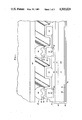
- FIG. 1 is a section view of a portion of a semiconductor device having a built up level contact in accordance with this invention.
- FIGS. 2 through 22 illustrate the sequence of process operations according to this invention which provide a semiconductor device with a built-up metal contact in accordance herewith.
- the device indicated generally at 10 includes a body of semiconductor material such as silicon indicated at 12 which includes a plurality of semiconductor regions therein.
- Body 12 includes a first major portion 14 and a second major portion 16 of n+ and n- conductivity types respectively.
- a wafer having such regions formed therein may be provided by epitaxially growing region 16 on a surface of an n+ conductivity type wafer 14.
- region 14 and region 16 together comprise the collector of the transistor, region 18 comprises the base and region 20 comprises the emitter.
- Contact is made to region 14 by per se conventional means which include 3 layer metalization 22, layer 24 of which may conveniently be a layer of chromiun, layer 26 a layer of nickel and layer 28 a layer of silver. Per se conventional means for applying such layers may be employed and one preferred method for so doing will be described in detail hereinbelow.
- An insulating and passivating layer 30 which is preferably a silicon dioxide layer is disposed on the upper surface of substrate 12 and is patterned and open to expose emitter 20 and a portion of base 18. It will be understood that in a transistor structure of the type illustrated herein that it is preferable to form the emitter and base regions as interdigitated structures such as opposing comb shaped regions to maximize the turn on area between the base and the emitter to maximize the amount of current and the switching speed characteristics thereof. Passivating layer 30 preferably overlaps the junction between emitter 20 and base 18 where the junction terminates at the surface.
- a relatively thick layer of aluminum, patterned to form emitter and base electrode portions 32 and 34 respectively is formed on the upper surface of substrate 12 as shown making ohmic contact to the emitter and base regions respectively.
- the thickness of the electrodes is primarily determined by the requirement for conducting substantial base current laterally along electrode 34 rather than by the higher emitter current requirements which are less significant inasmuch as current flow to emitter 20 is essentially vertical through electrode 32.
- Dielectric layer 36 covers insulating and passivating layer 30, base electrode 34 and emitter electrode 32.
- Dielectric layer 36 is open at the upper surface of electrode 32 to receive an upper level metalization including barrier layer 38 and solderable layers 40 disposed on emitter electrode 32 as well as solder layer 42 as shown.
- barrier layer 38 is a chromium layer
- solderable layer 40 includes one or more layers (two shown in FIG. 1) of copper and solder layer 42 is a lead-tin solder.
- the functions of barrier layer 38 and solderable layer 40 may be combined in a single layer such as a gold layer although possibly at increased cost which may, in certain applications, be offset by more simple fabrication.
- contact to base electrode 34 is made in a per se conventional way by fastening an electrical lead thereto at a contact portion located at the end of one or more of the fingers which may, as hereinabove described, be connected to a spine portion.
- Connection to emitter 20 of transistor 10 is made through a plate 43 which simultaneously contacts the upper metalization along its entire length and which is attached thereto by reflowing solder layer 42 with the metal plate in contact therewith.
- FIG. 1 provides a number of advantages over the prior art.
- Contact to emitter 20 is made vertically through electrode 32 and is not decreased by the lateral resistance of the electrode which introduces the problem hereinabove described in connection with prior art devices.
- contact to base 18 is made through electrode 34 and does, in fact depend on the lateral flow of current therein, nevertheless since the base current is typically many times less than the emitter current the effect of the lateral resistance of electrode 34 is not so great as to introduce intolerable voltage drops.
- FIGS. 2--22 show sequentially the operations involved in forming a semiconductor device such as has been illustrated and described hereinabove in connection with FIG. 1.
- a built-up metal contact begins by providing a semiconductor device such as is shown in FIG. 2 wherein a collector region including layers 14 and 16 of n+ and n- conductivity type respectively, a base layer 18 and an emitter layer 20.
- a collector region including layers 14 and 16 of n+ and n- conductivity type respectively, a base layer 18 and an emitter layer 20.
- the particular device in connection with which the invention is described is to some extent arbitary and as such forms no particular part of the invention and may be modified as, for example, by changing the conductivity types and the like in accordance with the requirements for particular devices.
- An oxide layer 30 as shown in FIG. 3 is applied to an upper surface of device 10 by per se conventional means. It will be appreciated that during the formation of device 10 to the stage illustrated at FIG. 2 various oxide masking layers may be employed for locating the several semiconductor regions and although, in FIG. 2, device 10 is shown with no oxide layers on the upper surface thereof, nevertheless oxide layers may exist such as the emitter mask oxide layer which need not necessarily be removed in accordance with this invention where the openings therein are disposed in the required locations for further processing. Nevertheless, for purposes of illustration, a new oxide layer 30 is shown which is patterned as shown in FIG. 4 and attached to form opening 50 over emitter 20.
- a layer of aluminum 52 having a thickness sufficient to conduct the aforementioned lateral base current signals is provided.
- a thickness of 60K ⁇ or more is preferred.
- Electrode 32 overlying emitter layer 20 will be understood to cover the entire emitter layer including such spine portions as are provided for joining the several emitter figures where a comb shaped structure is employed.
- each of the steps so far described in per se conventional and in accordance with existing practice a structure such as illustrated in FIG. 6 may be usefully employed by making electrical connection to the electrode 32 at a lead receiving portion such as the spine portion.
- the disadvantages attending such a construction have been heretofore described and are primarily related to the lateral resistance of the configuration of electrode 32 where substantial current flows therein in the direction parallel to the surface of device 10.
- the following steps represent an exemplary method for forming the structure illustrated in FIG. 1 and having all of the advantages thereof.
- a layer 36 of silicone polyimide siloxane is applied to the surface of device 10 over electrode 32. It is preferred to apply layer 36 in two coatings in order to improve the curing thereof. It is preferred to apply layer 36 by spinning a thin coating of polyimide material on the surface of the wafer and baking the thus applied layer at an elevated temperature to cure it. After curing of the first layer a second layer is applied and cured in a similar manner and finally the two layers may be fully cured at an even higher temperature to form a single homogeneous layer.
- the thickness of polyimide layer 36 should be sufficient to insure good coverage of aluminum electrode 32 especially at the edge thereof which may be of substantial height.
- polyimide layer 36 may be substituted for polyimide layer 36 provided the step coverage necessary to cover electrode 36 is obtainable and further provided that the material is capable of withstanding the temperatures involved in subsequent processing of the device.
- the polyimide layer has a total thickness of at least about 5 microns after final bake for the two coats applied.
- FIGS. 8-11 are directed to patterning the polyimide layer 36.
- a layer of polysilicon masking material 54 is deposited over polyimide layer 36.
- Polysilicon layer 54 is preferably deposited by electron beam evaporation techniques or other conventional methods to a thickness of about 1000 ⁇ .
- a layer of photoresist material 58 is deposited over polysilicon layer 54 and patterned.
- Shipley AZ1375 resist is employed and a layer having a thickness of about 3-4 microns is formed.
- Resist layer 58 is patterned and developed, for example, in AZ351 developer to form opening 60 therein aligned with an upper contact surface of aluminum electrode 32.
- Patterned photoresist layer 58 acts as a mask for subsequent etching of polysilicon layer 54 which then acts as a mask for polyimide layer 36.
- the removal of the polysilicon and polyimide layers proceeds in stages of a plasma etching process.
- a CF 4 plasma having a flow rate of about 20 standard cubic centimeters per minute (sccm) and about 2 sccm of oxygen is employed to pattern the polysilicon layer without affecting the polyimide or photoresist layer.
- the amount of oxygen is increased to about 50 sccm and the polyimide as well as the photoresist are removed.
- this second state of plasma etch portion of the process of this invention it is advantageous to increase the pressure in the plasma reactor somewhat to enhance the removal of polyimide material.
- FIG. 11 illustrates the final stage of the plasma etch process wherein the amount of oxygen is again reduced to about 2 sccm and the pressure is reduced to about 0.16 torr for removing the remaining portion of polysilicon layer 54.
- the remaining structure includes the semiconductor wafer, oxide layer 30, aluminum electrode 32 and patterned polyimide layer 36. An opening in polyimide layer 36 is in alignment with the upper surface of aluminum electrode 32.
- a layer of wax 64 is applied to the top surface of device 10 to protect the aluminum electrodes and polyimide layer thereof during subsequent processing.
- n+ layer 14 is a relatively low resistivity layer for enhancing contact to device and the thickness thereof is preferably minimized in order to reduce the resistance of the device in the on state.
- the initial thickness of layer 14 as shown in FIGS. 2--12 enhances the strength of the semiconductor wafer during the early stages of processing and thereby reduces the amount of breakage of such wafers.
- the wafers are rinsed in deionized wafer at a temperature not to exceed about 62° C. above which temperature the aluminum metalization begins to discolor.
- the formation of the chrome-nickel-silver metalization on the back surface of the semiconductor device proceeds in a manner per se well known to those skilled in the art.
- the chromium layer 68, nickel layer 70 and silver layer 72 are sequentially deposited in an evacuated chamber.
- a layer of chrome having a thickness of about 1K ⁇ , a layer of nickel having a thickness of about 4K ⁇ and a layer of silver having a thickness of about 15K ⁇ is deposited.
- the assembly is preferably sintered in nitrogen at about 450° for about 10 minutes.
- the device is ready for formation of the upper level metalization. Initially the device is cleaned in a hydrogen plasma at a slightly elevated temperature to provide a surface for accepting barrier layer 74. Immediately after plasma etching device 10, the upper layer metalization process is commenced by sputter etching the upper surface of the device to remove any oxide which may have formed thereon and to improve adhesion to the aluminum layer. Without removing the device from the sputtering chamber a layer of chromium 74 having a thickness of about 2000 ⁇ followed by a layer of copper 76 having a thickness of about 8000 ⁇ and finally followed by a layer of titanium 78 having a thickness of about 1000 ⁇ is applied as illustrated in FIG. 16.
- the chromium layer provides a barrier between the aluminum and the copper for preventing interaction thereof which would degrade the contact therebetween.
- the copper layer is employed to provide a solderable surface to which the solder bump itself may be attached and the titanium layer prevents the oxidation of the copper layer prior to the formation of the solder bump.
- solder bump itself is illustrated in FIGS. 17-22 and commences with the application of a layer of photoresist 80 over the top of the titanium layer 78, which is patterned in a conventional manner to form opening 82 therein which exposes copper layer 76.
- a photoresist such as AZ119 green resist is employed which is developed with a type AZ303 developer.
- a layer of wax 79 is applied to the back surface of device 10 over the chrome-nickel-silver metalization thereon to protect the same during the following etching steps.
- the portion of titanium layer 78 exposed by opening 82 in photoresist layer 80 is etched according to conventional methods and the exposed surface of copper layer 76 is cleaned, for example, in 10% sulphuric acid and rinsed in deionized water to present a surface for the following copper plating operation.
- FIG. 19 illustrates the formation by plating of a copper layer 86 on the surface of copper layer 76.
- Copper layer 86 is preferably plated to a thickness of at least 1/2 mil.
- a layer of lead 88 followed by a layer of tin 90 is sequentially plated on the surface of copper layer 86.
- the amount of lead and tin plated onto the device is determined by the ratio of lead to tin desired in the ultimate solder bump. It is preferred in accordance with this invention to have about 95% lead and 5% tin.
- the overall height of the lead-tin bump is at least about 2 mils.
- the photoresist After the formation of the lead-in solder bump the photoresist, titanium, copper and chromium layers overlying the polyimide dielectric layer on the upper surface as well as the wax on the lower surface are removed.
- the photoresist is removed in acetone followed by a cold deionized water rinse.
- the titanium layer is removed in 10% fluoboric acid.
- the copper layer is then removed by etching in a copper etch and finally the chromium layer is removed by etching in hydrochloric acid. Finally the structure is rinsed in cold deionized water and dried.
- the mounting of the top plate to the device proceeds initially by reflowing the lead-tin layers at a temperature of about 360° C. to form a lead-in alloy ball in the form of a layer which conforms to the lateral configuration of the underlying solderable layer.
- the surface tension of the lead-tin alloy layer will cause it to assume a generally round cross-sectional shape throughout the aforesaid lateral configuration which advantageously increases the height thereof.
- Soldering of the upper metal plate to the upstanding solder layer is accomplished by merely placing the clean plate on the device in contact with the lead-tin alloy solder bumps and heating the structure to cause the solder to reflow and wet the lower surface of the plate and to solder thereto thus producing the structure of FIG. 1.
- the essential elements of the invention include an electrode on a semiconductor region which contacts the semiconductor region essentially along the entire length thereof especially in the case of an emitter region of a transistor or the like wherein a long relatively narrow region is contacted by an electrode of similar shape and even more particularly where such a region or plurality of regions is joined to a spine portion at one end thereof for interconnecting the various long, narrow regions.
- Current flow through such an electrode is accomplished by connecting the electrode to an upper plate through an upper level metalization including a barrier layer on said electrode and a solder bump on said barrier layer which solder bump may be directly connected to the upper level plate.
- an emitter which takes the form of a plurality of isolated regions such as dots.
- This invention is ideally suited to make connection to such a structure.
Abstract
Description
Claims (8)
Priority Applications (1)
| Application Number | Priority Date | Filing Date | Title |
|---|---|---|---|
| US06/501,745 US4505029A (en) | 1981-03-23 | 1983-07-08 | Semiconductor device with built-up low resistance contact |
Applications Claiming Priority (2)
| Application Number | Priority Date | Filing Date | Title |
|---|---|---|---|
| US24623181A | 1981-03-23 | 1981-03-23 | |
| US06/501,745 US4505029A (en) | 1981-03-23 | 1983-07-08 | Semiconductor device with built-up low resistance contact |
Related Parent Applications (1)
| Application Number | Title | Priority Date | Filing Date |
|---|---|---|---|
| US24623181A Continuation | 1981-03-23 | 1981-03-23 |
Publications (1)
| Publication Number | Publication Date |
|---|---|
| US4505029A true US4505029A (en) | 1985-03-19 |
Family
ID=26937812
Family Applications (1)
| Application Number | Title | Priority Date | Filing Date |
|---|---|---|---|
| US06/501,745 Expired - Lifetime US4505029A (en) | 1981-03-23 | 1983-07-08 | Semiconductor device with built-up low resistance contact |
Country Status (1)
| Country | Link |
|---|---|
| US (1) | US4505029A (en) |
Cited By (32)
| Publication number | Priority date | Publication date | Assignee | Title |
|---|---|---|---|---|
| US4617723A (en) * | 1982-12-28 | 1986-10-21 | Fujitsu Limited | Method and device for creating an activatable conducting link in a semiconductor device |
| US4661375A (en) * | 1985-04-22 | 1987-04-28 | At&T Technologies, Inc. | Method for increasing the height of solder bumps |
| DE3637513A1 (en) * | 1986-11-04 | 1988-05-11 | Semikron Elektronik Gmbh | Method of producing finely structured contact electrodes of power semiconductor components |
| US4789647A (en) * | 1986-01-08 | 1988-12-06 | U.S. Philips Corporation | Method of manufacturing a semiconductor device, in which a metallization with a thick connection electrode is provided on a semiconductor body |
| US4953003A (en) * | 1987-05-21 | 1990-08-28 | Siemens Aktiengesellschaft | Power semiconductor device |
| US5101259A (en) * | 1987-07-31 | 1992-03-31 | Kabushiki Kaisha Toshiba | Semiconductor device and manufacturing method thereof |
| US5130275A (en) * | 1990-07-02 | 1992-07-14 | Digital Equipment Corp. | Post fabrication processing of semiconductor chips |
| US5404265A (en) * | 1992-08-28 | 1995-04-04 | Fujitsu Limited | Interconnect capacitors |
| US5445998A (en) * | 1992-11-20 | 1995-08-29 | Deutsche Itt Industries Gmbh | Method for the global planarization of surfaces of semiconductor integrated circuits |
| US5471092A (en) * | 1992-09-15 | 1995-11-28 | International Business Machines Corporation | Metallurgical joint including a stress release layer |
| US5796591A (en) * | 1995-06-07 | 1998-08-18 | International Business Machines Corporation | Direct chip attach circuit card |
| US5895228A (en) * | 1996-11-14 | 1999-04-20 | International Business Machines Corporation | Encapsulation of organic light emitting devices using Siloxane or Siloxane derivatives |
| US5918144A (en) * | 1996-08-29 | 1999-06-29 | Sony Corporation | Method of manufacturing a semiconductor device |
| US6221692B1 (en) * | 1997-08-25 | 2001-04-24 | Showa Denko, K.K. | Method of fabricating solder-bearing silicon semiconductor device and circuit board mounted therewith |
| US6239494B1 (en) * | 1999-04-21 | 2001-05-29 | Advanced Micro Devices, Inc. | Wire bonding CU interconnects |
| US6251775B1 (en) * | 1999-04-23 | 2001-06-26 | International Business Machines Corporation | Self-aligned copper silicide formation for improved adhesion/electromigration |
| US6340630B1 (en) * | 1996-09-25 | 2002-01-22 | International Business Machines Corporation | Method for making interconnect for low temperature chip attachment |
| US6492197B1 (en) * | 2000-05-23 | 2002-12-10 | Unitive Electronics Inc. | Trilayer/bilayer solder bumps and fabrication methods therefor |
| US20030008489A1 (en) * | 2001-05-04 | 2003-01-09 | Tessera, Inc. | Method of making bondable leads using positive photoresist and structures made therefrom |
| US6740427B2 (en) * | 2001-09-21 | 2004-05-25 | Intel Corporation | Thermo-mechanically robust C4 ball-limiting metallurgy to prevent failure due to die-package interaction and method of making same |
| US20040102022A1 (en) * | 2002-11-22 | 2004-05-27 | Tongbi Jiang | Methods of fabricating integrated circuitry |
| US20040159944A1 (en) * | 2001-09-21 | 2004-08-19 | Madhav Datta | Copper-containing C4 ball-limiting metallurgy stack for enhanced reliability of packaged structures and method of making same |
| US20040209406A1 (en) * | 2003-02-18 | 2004-10-21 | Jong-Rong Jan | Methods of selectively bumping integrated circuit substrates and related structures |
| US20050279809A1 (en) * | 2000-11-10 | 2005-12-22 | Rinne Glenn A | Optical structures including liquid bumps and related methods |
| US20060076679A1 (en) * | 2002-06-25 | 2006-04-13 | Batchelor William E | Non-circular via holes for bumping pads and related structures |
| US7156284B2 (en) | 2000-12-15 | 2007-01-02 | Unitive International Limited | Low temperature methods of bonding components and related structures |
| US20080210301A1 (en) * | 2003-04-10 | 2008-09-04 | Sunpower Corporation | Metal contact structure for solar cell and method of manufacture |
| US7547623B2 (en) | 2002-06-25 | 2009-06-16 | Unitive International Limited | Methods of forming lead free solder bumps |
| US20100004251A1 (en) * | 2004-02-18 | 2010-01-07 | Sepracor Inc. | Dopamine-Agonist Combination Therapy For Improving Sleep Quality |
| US20100032802A1 (en) * | 2008-08-11 | 2010-02-11 | Texas Instruments Incorporated | Assembling of Electronic Members on IC Chip |
| US7879715B2 (en) | 2002-06-25 | 2011-02-01 | Unitive International Limited | Methods of forming electronic structures including conductive shunt layers and related structures |
| US20120025369A1 (en) * | 2010-08-02 | 2012-02-02 | Chung-Yao Kao | Semiconductor package |
Citations (9)
| Publication number | Priority date | Publication date | Assignee | Title |
|---|---|---|---|---|
| US27934A (en) * | 1860-04-17 | Eyelet-machine | ||
| US3392442A (en) * | 1965-06-24 | 1968-07-16 | Ibm | Solder method for providing standoff of device from substrate |
| US3458925A (en) * | 1966-01-20 | 1969-08-05 | Ibm | Method of forming solder mounds on substrates |
| US3508118A (en) * | 1965-12-13 | 1970-04-21 | Ibm | Circuit structure |
| US3585461A (en) * | 1968-02-19 | 1971-06-15 | Westinghouse Electric Corp | High reliability semiconductive devices and integrated circuits |
| US3585713A (en) * | 1968-03-25 | 1971-06-22 | Sony Corp | Method of making connecting parts of semiconductor devices or the like |
| US3761309A (en) * | 1970-07-02 | 1973-09-25 | Siemens Ag | Ctor components into housings method of producing soft solderable contacts for installing semicondu |
| US3881884A (en) * | 1973-10-12 | 1975-05-06 | Ibm | Method for the formation of corrosion resistant electronic interconnections |
| US4017886A (en) * | 1972-10-18 | 1977-04-12 | Hitachi, Ltd. | Discrete semiconductor device having polymer resin as insulator and method for making the same |
-
1983
- 1983-07-08 US US06/501,745 patent/US4505029A/en not_active Expired - Lifetime
Patent Citations (9)
| Publication number | Priority date | Publication date | Assignee | Title |
|---|---|---|---|---|
| US27934A (en) * | 1860-04-17 | Eyelet-machine | ||
| US3392442A (en) * | 1965-06-24 | 1968-07-16 | Ibm | Solder method for providing standoff of device from substrate |
| US3508118A (en) * | 1965-12-13 | 1970-04-21 | Ibm | Circuit structure |
| US3458925A (en) * | 1966-01-20 | 1969-08-05 | Ibm | Method of forming solder mounds on substrates |
| US3585461A (en) * | 1968-02-19 | 1971-06-15 | Westinghouse Electric Corp | High reliability semiconductive devices and integrated circuits |
| US3585713A (en) * | 1968-03-25 | 1971-06-22 | Sony Corp | Method of making connecting parts of semiconductor devices or the like |
| US3761309A (en) * | 1970-07-02 | 1973-09-25 | Siemens Ag | Ctor components into housings method of producing soft solderable contacts for installing semicondu |
| US4017886A (en) * | 1972-10-18 | 1977-04-12 | Hitachi, Ltd. | Discrete semiconductor device having polymer resin as insulator and method for making the same |
| US3881884A (en) * | 1973-10-12 | 1975-05-06 | Ibm | Method for the formation of corrosion resistant electronic interconnections |
Cited By (59)
| Publication number | Priority date | Publication date | Assignee | Title |
|---|---|---|---|---|
| US4617723A (en) * | 1982-12-28 | 1986-10-21 | Fujitsu Limited | Method and device for creating an activatable conducting link in a semiconductor device |
| US4661375A (en) * | 1985-04-22 | 1987-04-28 | At&T Technologies, Inc. | Method for increasing the height of solder bumps |
| US4789647A (en) * | 1986-01-08 | 1988-12-06 | U.S. Philips Corporation | Method of manufacturing a semiconductor device, in which a metallization with a thick connection electrode is provided on a semiconductor body |
| DE3637513A1 (en) * | 1986-11-04 | 1988-05-11 | Semikron Elektronik Gmbh | Method of producing finely structured contact electrodes of power semiconductor components |
| US4953003A (en) * | 1987-05-21 | 1990-08-28 | Siemens Aktiengesellschaft | Power semiconductor device |
| US5302548A (en) * | 1987-07-31 | 1994-04-12 | Kabushiki Kaisha Toshiba | Semiconductor device manufacturing method |
| US5101259A (en) * | 1987-07-31 | 1992-03-31 | Kabushiki Kaisha Toshiba | Semiconductor device and manufacturing method thereof |
| US5130275A (en) * | 1990-07-02 | 1992-07-14 | Digital Equipment Corp. | Post fabrication processing of semiconductor chips |
| US5277756A (en) * | 1990-07-02 | 1994-01-11 | Digital Equipment Corporation | Post fabrication processing of semiconductor chips |
| US5404265A (en) * | 1992-08-28 | 1995-04-04 | Fujitsu Limited | Interconnect capacitors |
| US5471092A (en) * | 1992-09-15 | 1995-11-28 | International Business Machines Corporation | Metallurgical joint including a stress release layer |
| US5445998A (en) * | 1992-11-20 | 1995-08-29 | Deutsche Itt Industries Gmbh | Method for the global planarization of surfaces of semiconductor integrated circuits |
| US5796591A (en) * | 1995-06-07 | 1998-08-18 | International Business Machines Corporation | Direct chip attach circuit card |
| US5918144A (en) * | 1996-08-29 | 1999-06-29 | Sony Corporation | Method of manufacturing a semiconductor device |
| US6340630B1 (en) * | 1996-09-25 | 2002-01-22 | International Business Machines Corporation | Method for making interconnect for low temperature chip attachment |
| US5895228A (en) * | 1996-11-14 | 1999-04-20 | International Business Machines Corporation | Encapsulation of organic light emitting devices using Siloxane or Siloxane derivatives |
| US6221692B1 (en) * | 1997-08-25 | 2001-04-24 | Showa Denko, K.K. | Method of fabricating solder-bearing silicon semiconductor device and circuit board mounted therewith |
| US6239494B1 (en) * | 1999-04-21 | 2001-05-29 | Advanced Micro Devices, Inc. | Wire bonding CU interconnects |
| US6818992B1 (en) | 1999-04-23 | 2004-11-16 | International Business Machines Corporation | Self-aligned copper silicide formation for improved adhesion/electromigration |
| US6251775B1 (en) * | 1999-04-23 | 2001-06-26 | International Business Machines Corporation | Self-aligned copper silicide formation for improved adhesion/electromigration |
| US6492197B1 (en) * | 2000-05-23 | 2002-12-10 | Unitive Electronics Inc. | Trilayer/bilayer solder bumps and fabrication methods therefor |
| US20070152020A1 (en) * | 2000-11-10 | 2007-07-05 | Unitive International Limited | Optical structures including liquid bumps |
| US7213740B2 (en) | 2000-11-10 | 2007-05-08 | Unitive International Limited | Optical structures including liquid bumps and related methods |
| US20050279809A1 (en) * | 2000-11-10 | 2005-12-22 | Rinne Glenn A | Optical structures including liquid bumps and related methods |
| US7156284B2 (en) | 2000-12-15 | 2007-01-02 | Unitive International Limited | Low temperature methods of bonding components and related structures |
| US20060030140A1 (en) * | 2001-05-04 | 2006-02-09 | Tessera, Inc. | Method of making bondable leads using positive photoresist and structures made therefrom |
| US7087510B2 (en) * | 2001-05-04 | 2006-08-08 | Tessera, Inc. | Method of making bondable leads using positive photoresist and structures made therefrom |
| US20030008489A1 (en) * | 2001-05-04 | 2003-01-09 | Tessera, Inc. | Method of making bondable leads using positive photoresist and structures made therefrom |
| US6853076B2 (en) | 2001-09-21 | 2005-02-08 | Intel Corporation | Copper-containing C4 ball-limiting metallurgy stack for enhanced reliability of packaged structures and method of making same |
| US20100117229A1 (en) * | 2001-09-21 | 2010-05-13 | Madhav Datta | Copper-containing C4 ball-limiting metallurgy stack for enhanced reliability of packaged structures and method of making same |
| US10037956B2 (en) | 2001-09-21 | 2018-07-31 | Intel Corporation | Copper-containing C4 ball-limiting metallurgy stack for enhanced reliability of packaged structures and method of making same |
| US8952550B2 (en) | 2001-09-21 | 2015-02-10 | Intel Corporation | Copper-containing C4 ball-limiting metallurgy stack for enhanced reliability of packaged structures and method of making same |
| US7250678B2 (en) | 2001-09-21 | 2007-07-31 | Intel Corporation | Copper-containing C4 ball-limiting metallurgy stack for enhanced reliability of packaged structures and method of making same |
| US20060148233A1 (en) * | 2001-09-21 | 2006-07-06 | Madhav Datta | Copper-containing C4 ball-limiting metallurgy stack for enhanced reliability of packaged structures and method of making same |
| US6740427B2 (en) * | 2001-09-21 | 2004-05-25 | Intel Corporation | Thermo-mechanically robust C4 ball-limiting metallurgy to prevent failure due to die-package interaction and method of making same |
| US7196001B2 (en) | 2001-09-21 | 2007-03-27 | Intel Corporation | Copper-containing C4 ball-limiting metallurgy stack for enhanced reliability of packaged structures and method of making same |
| US20040159947A1 (en) * | 2001-09-21 | 2004-08-19 | Madhav Datta | Copper-containing C4 ball-limiting metallurgy stack for enhanced reliability of packaged structures and method of making same |
| US20040159944A1 (en) * | 2001-09-21 | 2004-08-19 | Madhav Datta | Copper-containing C4 ball-limiting metallurgy stack for enhanced reliability of packaged structures and method of making same |
| US20090212427A1 (en) * | 2002-06-25 | 2009-08-27 | Unitive International Limited | Solder Structures Including Barrier Layers with Nickel and/or Copper |
| US20110084392A1 (en) * | 2002-06-25 | 2011-04-14 | Nair Krishna K | Electronic Structures Including Conductive Layers Comprising Copper and Having a Thickness of at Least 0.5 Micrometers |
| US7879715B2 (en) | 2002-06-25 | 2011-02-01 | Unitive International Limited | Methods of forming electronic structures including conductive shunt layers and related structures |
| US7839000B2 (en) | 2002-06-25 | 2010-11-23 | Unitive International Limited | Solder structures including barrier layers with nickel and/or copper |
| US20060076679A1 (en) * | 2002-06-25 | 2006-04-13 | Batchelor William E | Non-circular via holes for bumping pads and related structures |
| US8294269B2 (en) | 2002-06-25 | 2012-10-23 | Unitive International | Electronic structures including conductive layers comprising copper and having a thickness of at least 0.5 micrometers |
| US7531898B2 (en) | 2002-06-25 | 2009-05-12 | Unitive International Limited | Non-Circular via holes for bumping pads and related structures |
| US7547623B2 (en) | 2002-06-25 | 2009-06-16 | Unitive International Limited | Methods of forming lead free solder bumps |
| US20060030077A1 (en) * | 2002-11-22 | 2006-02-09 | Micron Technology, Inc. | Substrate comprising a plurality of integrated circuitry die, and a substrate |
| US20060030078A1 (en) * | 2002-11-22 | 2006-02-09 | Tongbi Jiang | Methods of fabricating integrated circuitry |
| US7078267B2 (en) | 2002-11-22 | 2006-07-18 | Micron Technology, Inc. | Methods of fabricating integrated circuitry |
| US20040102022A1 (en) * | 2002-11-22 | 2004-05-27 | Tongbi Jiang | Methods of fabricating integrated circuitry |
| US8461685B2 (en) | 2002-11-22 | 2013-06-11 | Micron Technology, Inc. | Substrate comprising a plurality of integrated circuitry die, and a substrate |
| US7579694B2 (en) | 2003-02-18 | 2009-08-25 | Unitive International Limited | Electronic devices including offset conductive bumps |
| US20040209406A1 (en) * | 2003-02-18 | 2004-10-21 | Jong-Rong Jan | Methods of selectively bumping integrated circuit substrates and related structures |
| US20060231951A1 (en) * | 2003-02-18 | 2006-10-19 | Jong-Rong Jan | Electronic devices including offset conductive bumps |
| US7081404B2 (en) | 2003-02-18 | 2006-07-25 | Unitive Electronics Inc. | Methods of selectively bumping integrated circuit substrates and related structures |
| US20080210301A1 (en) * | 2003-04-10 | 2008-09-04 | Sunpower Corporation | Metal contact structure for solar cell and method of manufacture |
| US20100004251A1 (en) * | 2004-02-18 | 2010-01-07 | Sepracor Inc. | Dopamine-Agonist Combination Therapy For Improving Sleep Quality |
| US20100032802A1 (en) * | 2008-08-11 | 2010-02-11 | Texas Instruments Incorporated | Assembling of Electronic Members on IC Chip |
| US20120025369A1 (en) * | 2010-08-02 | 2012-02-02 | Chung-Yao Kao | Semiconductor package |
Similar Documents
| Publication | Publication Date | Title |
|---|---|---|
| US4505029A (en) | Semiconductor device with built-up low resistance contact | |
| KR100264479B1 (en) | Structure of bump electrode and method of forming the same | |
| KR0166967B1 (en) | Bump structure of reflow bonding of ic device | |
| US8169063B2 (en) | Semiconductor component and method for producing the same | |
| US5892273A (en) | Semiconductor package integral with semiconductor chip | |
| US7902679B2 (en) | Structure and manufacturing method of a chip scale package with low fabrication cost, fine pitch and high reliability solder bump | |
| US20060175686A1 (en) | Semiconductor device and fabrication method thereof | |
| US3501681A (en) | Face bonding of semiconductor devices | |
| US6084312A (en) | Semiconductor devices having double pad structure | |
| US5047833A (en) | Solderable front metal contact for MOS devices | |
| KR20050087840A (en) | Structure and method for bonding to copper interconnect structures | |
| US10049997B2 (en) | Semiconductor device and method of fabricating the same | |
| CA1197629A (en) | Semiconductor device with built-up low resistance contact | |
| KR100428825B1 (en) | Semiconductor integrated circuit and fabrication process therefor | |
| US6649507B1 (en) | Dual layer photoresist method for fabricating a mushroom bumping plating structure | |
| US20080017993A1 (en) | Semiconductor device and method of manufacturing the same | |
| US3543106A (en) | Microminiature electrical component having indexable relief pattern | |
| JPS63177463A (en) | Manufacture of contact electrode composed of fine structure for power semiconductor component | |
| US3836446A (en) | Semiconductor devices manufacture | |
| US5396702A (en) | Method for forming solder bumps on a substrate using an electrodeposition technique | |
| US4672415A (en) | Power thyristor on a substrate | |
| JPH0758112A (en) | Semiconductor device | |
| KR100612188B1 (en) | Schottky barrier diode and manufacturing method of the same | |
| KR0169471B1 (en) | Bipolar bump transistor and method for its manufacture | |
| KR100612186B1 (en) | Schottky barrier diode and method of fabricating the same |
Legal Events
| Date | Code | Title | Description |
|---|---|---|---|
| STCF | Information on status: patent grant |
Free format text: PATENTED CASE |
|
| FPAY | Fee payment |
Year of fee payment: 4 |
|
| FPAY | Fee payment |
Year of fee payment: 8 |
|
| FPAY | Fee payment |
Year of fee payment: 12 |
|
| FEPP | Fee payment procedure |
Free format text: PAYOR NUMBER ASSIGNED (ORIGINAL EVENT CODE: ASPN); ENTITY STATUS OF PATENT OWNER: LARGE ENTITY |
|
| AS | Assignment |
Owner name: INTERSIL CORPORATION, FLORIDA Free format text: ASSIGNMENT OF ASSIGNORS INTEREST;ASSIGNOR:HARRIS CORPORATION;REEL/FRAME:010255/0405 Effective date: 19990813 |
|
| AS | Assignment |
Owner name: CREDIT SUISSE FIRST BOSTON, AS COLLATERAL AGENT, N Free format text: SECURITY INTEREST;ASSIGNOR:INTERSIL CORPORATION;REEL/FRAME:010351/0410 Effective date: 19990813 |
|
| AS | Assignment |
Owner name: INTERSIL HOLDING CORPORATION, CALIFORNIA Free format text: INTELLECTUAL PROPERTY PARTIAL RELEASE;ASSIGNOR:CREIDT SUISSE FIRST BOSTON;REEL/FRAME:011667/0166 Effective date: 20010303 |
|
| AS | Assignment |
Owner name: FAIRCHILD SEMICONDUCTOR CORPORATION, MAINE Free format text: REASSIGNMENT OF PATENT APPLICATIONS;ASSIGNOR:INTERSIL CORPORATION;REEL/FRAME:012002/0206 Effective date: 20010406 |