US4367471A - Arrangement for actuating controllable diode elements - Google Patents
Arrangement for actuating controllable diode elements Download PDFInfo
- Publication number
- US4367471A US4367471A US06/240,546 US24054681A US4367471A US 4367471 A US4367471 A US 4367471A US 24054681 A US24054681 A US 24054681A US 4367471 A US4367471 A US 4367471A
- Authority
- US
- United States
- Prior art keywords
- group
- pairs
- diodes
- diode
- diode pairs
- Prior art date
- Legal status (The legal status is an assumption and is not a legal conclusion. Google has not performed a legal analysis and makes no representation as to the accuracy of the status listed.)
- Expired - Lifetime
Links
Images


Classifications
-
- G—PHYSICS
- G09—EDUCATION; CRYPTOGRAPHY; DISPLAY; ADVERTISING; SEALS
- G09F—DISPLAYING; ADVERTISING; SIGNS; LABELS OR NAME-PLATES; SEALS
- G09F9/00—Indicating arrangements for variable information in which the information is built-up on a support by selection or combination of individual elements
- G09F9/30—Indicating arrangements for variable information in which the information is built-up on a support by selection or combination of individual elements in which the desired character or characters are formed by combining individual elements
- G09F9/33—Indicating arrangements for variable information in which the information is built-up on a support by selection or combination of individual elements in which the desired character or characters are formed by combining individual elements being semiconductor devices, e.g. diodes
Definitions
- the present invention relates to an arrangement for actuating controllable elements, for example light-emitting diodes in an information display.
- LEDs light-emitting diodes
- These arrangements which are called LED displays, have a number of advantages such as their low operating voltage, their rapid response time, the possibility of multiplex operation, a broad range of operating temperature, robustness and a long life span.
- the number of LED's required depends on the respective application. For a digit display (0-9) including a decimal point, for example, 8 LED's are required, 14-35 LED's are required for letter characters, 100 LED's are required for strip display with 1% definition and more than 1,000 LED's are required for a viewing screen.
- a relatively large number of supply lines is generally required to control or trigger the LED's. If, for example, the cathodes of all of the LED's are connected together and if each diode is individually controlled, n supply lines are required to control n-1 diodes. In addition, there is the system of so-called matrix wiring which can control n 2 /4 diodes with n supply lines.
- matrix wiring reduces the number of supply lines, a relatively large number of supply lines is still required if there are very many LED's.
- the large number of supply lines required in many cases represents a serious problem in implementing diode displays.
- matrix wiring lines always cross and this is not advantageous.
- the object underlying the invention is to provide an arrangement for displaying information which operates with as few supply lines as possible in order to control the display and in which no lines cross.
- an arrangement comprising a plurality of light-emitting diodes said diodes being arranged in 2n-3 pairs, where n is an integer greater than 2, the diodes of each pair being mutually connected in antiparallel, n supply conductors, said supply conductors being arranged to control said 2n-3 pairs of diodes, further conductors, said pairs of diodes being interconnected by said further conductors, wherein none of said conductors cross.
- FIGS. 1a-c show three embodiments of the present invention
- FIGS. 2a-c show three further embodiments of the present invention.
- FIG. 3 shows another embodiment of the invention which combines features of the embodiments of FIGS. 1 and 2.
- the diode display has two groups of diode pairs, for example, in which the LED's of each diode pair are connected antiparallel of each other in each case.
- the diode pairs of the first group are connected together in a continuous chain to form a closed ring.
- the connection points between the diode pairs in the first group are provided with supply lines.
- all of the diode pairs are connected at one of their two ends to a point which is located between two diode pairs of the chain of the first group.
- the other ends of the diode pairs of the second group are also connected to connection points between the diode pairs of the chain of the first group.
- this is implemented such that only one pair of diodes of the second group in each case is connected to such a connection point and such that there is no pair of diodes of the second group connected to the two connection points which are only separated from the connection point which serves as a common connection for the diode pairs of the second group by a single diode pair of the chain of the first group.
- a first group of diode pairs connected together in a continuous chain to form a closed ring is also provided, the connection points between the diode pairs of the chain also being provided with supply lines.
- a second group of diode pairs which forms a second chain which is a closed ring when there is an even number of diode pairs in the first chain and is not closed when there is an odd number of diode pairs in the first chain.
- Each diode pair of the second group is connected in parallel with a series circuit comprising two diode pairs of the first group in this diode display.
- a further or several further groups of diode pairs are provided.
- a further group of diode pairs is provided in each case where the number of diode pairs of the group which has the next but one larger number of diodes as compared to the further group is even and the group having the next larger number of diode pairs has more than three diode pairs.
- a further group is also provided in each case when the number of diode pairs of the group having the next but one larger number of diode pairs is an odd number and the number of diode pairs of the group with the next larger number of diode pairs is greater than two.
- this further group is connected to the group having the next larger number of diode pairs, when the number of diode pairs of the group having the next but one larger number of diode pairs is even, in the same way as the group having the next larger number of diode pairs is connected to the group having the next but one larger number of diode pairs.
- the further group is connected to the chain comprising the group with the next larger number of diode pairs as compared to the further group and a diode pair from the group having the next but one larger number of diode pairs in the same way as the group having the next larger number of diode pairs is connected to the group with the next but one larger number of diode pairs.
- the diodes of the diode pairs are also connected antiparallel of each other.
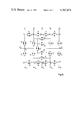
- FIG. 1a shows a diode display according to the invention having 8 supply lines and 13 pairs of diodes connected antiparallel to each other, i.e. a total of 26 diodes.
- a first group of 8 pairs of diodes P 1 to P 8 can be seen in a continuous chain to form a closed ring.
- the connection points V 1 to V 8 between the diode pairs P 1 to P 8 are provided with 8 supply lines Z 1 to Z 8 .
- a second group of 5 diode pairs P 1 ' to P 5 ' is provided.
- the diode pairs P 1 ' to P 5 ' are connected at their one end jointly to the connection point V 6 and therefore to the supply line Z 6 .
- the common connection of the diode pairs P 1 ' to P 5 ' may also be connected to any other of the connection points V 1 to V 8 however.
- the other ends of the diode pairs P 1 ' to P 5 ' are in each case connected to another connection point and in fact diode pairs P 1 ' is connected to a connection point V 2 , P 2 ' is connected to V 3 , P 3 ' is connected to V 4 , P 4 ' is connected to V 8 and P 5 ' is connected to V 1 . It can be seen that in each case one diode pair of the group P 1 ' to P 5 ' is connected to connection points V 1 , V 2 , V 3 , V 4 and V 8 .
- connection points V 5 and V 7 are separated from the common connection point V 6 by the diode pairs P 5 and P 6 of the first group.
- FIG. 1b shows a different embodiment of the invention in which, in contrast to the embodiment of FIG. 1a, the connection point V 1 is connected to all 5 diode pairs P 1 ' to P 5 ' of the second group. In other respects the embodiment of FIG. 1b corresponds to that of FIG. 1a.
- FIG. 1c shows a further embodiment of the invention in which the arrangement of diodes is selected so that a line arrangement is achieved.
- 9 supply lines Z 1 to Z 9 are provided, 9 diode pairs P 1 to P 9 of the first group, and 6 diode pairs (P 1 ' to P 6 ') of the second group, so that there are a total of 30 diodes.
- FIGS. 2a and 2c show further examples of embodiments of the invention in which the first group has an even number of diode pairs, while in the example of embodiment of FIG. 2b there is an odd number of diode pairs in the first group.
- FIG. 2a shows a first group of diode pairs P 1 to P 8 which are connected together in a continuous chain to form a closed ring. Connection points V 1 to V 8 between the diode pairs P 1 to P 8 are provided with supply lines (Z 1 to Z 8 ).
- FIG. 2a also shows a second group of four diode pairs P 1 ' to P 4 ' which form a second closed ring because the first group has an even number of diode pairs.
- Each diode pair of the second chain is connected in parallel with a series circuit of two diode pairs of the first chain in each case, i.e.
- a further group i.e. a third group of diode pairs is provided because the conditions that the group with the next but one larger number of diode pairs as compared to the third group, i.e. the first group, has an even number of diode pairs and that the group with the next larger number of diode pairs, i.e.
- the third group has only one diode pair in the arrangement of FIG. 2a, however in the arrangement of FIG. 2c the third group has three diode pairs.
- the diode pair P 1 " of the third group is connected to the second group (P 1 ' to P 4 ') in the same way as the second group (P 1 ' to P 4 ') is connected to the first group (P 1 to P.sub. 8), i.e. P 1 " is connected in parallel to the series circuit comprising P 1 ' and P 4 ' and parallel to the series circuit comprising P 2 ' and P 3 '.
- a first group of nine diode pairs P 1 to P 9 is present, these diode pairs being connected together to form a closed ring chain.
- the connection points V 1 to V 9 between the diode pairs P 1 to P 9 are provided with supply lines.
- the arrangement of FIG. 2b also has a second group of four diode pairs P 1 ' to P 4 ', these diode pairs forming a second chain which is however not closed because the first group (P 1 to P 9 ) has an odd number of diode pairs.
- Each diode pair of the second chain (P 1 ' to P 4 ') is connected in parallel to a series circuit of two diode pairs of the first chain in each case and in fact P 1 ' is connected parallel to the series circuit comprising P 9 and P 1 , P 2 ' is connected parallel to the series circuit comprising P 3 and P 4 , P 3 ' is connected parallel to the series circuit comprising P 5 and P 6 and P 4 ' is connected parallel to the series circuit comprising P 7 and P 8 .
- 2b also has a third group (P 1 " and P 2 ") of diode pairs as a further group, because the group with the next but one larger number of diode pairs as compared to the third group, i.e. the first group (P 1 to P 9 ), has an odd number of diode pairs and because the group with the next larger number of diode pairs, i.e. the second group (P 1 ' to P 4 '), has four diode pairs, i.e. at least three diode pairs.
- the group having the next but one larger number of diodes i.e. the first group
- the diode pairs of the third group are connected to the diode pairs of a chain, which has yet to be defined, in the same manner as the diode pairs of the group with the next larger number of diode pairs is connected to the diode pairs of the group with the next but one larger number of diode pairs. Consequently, in the arrangement of FIG.
- the diode pairs (P 1 " and P 2 ") of the third group are connected to the diode pairs of a particular chain in the same manner as the diode pairs (P 1 ' to P 4 ') of the second group (group with the next larger number of diode pairs) are connected to the diode pairs (P 1 to P 9 ) of the first group, i.e. the group with the next but one larger number of diode pairs.
- the particular chain which is used to connect the diode pairs of the third group in the manner described comprises the second group (P 1 ' to P 4 '), i.e.
- the group with the next larger number of diode pairs, as compared to the further (third) group and the diode pair (P 2 ) from the first group, i.e. the group with the next but one larger number of diode pairs as compared to the third group.
- the diode pairs (P 1 " and P 2 ") of the third group are connected to the chain formed from diode pairs (P1' to P4') of the second group and a diode pair (P 2 ) from the first group in the same way as the diode pairs (P 1 ' to P 4 ') of the second group are connected to the diode pairs (P 1 to P 9 ) from the first group, P 1 " is connected parallel to the series circuit comprising P 1 ' and P 2 ' and P 2 " is connected parallel to the series circuit comprising P 3 ' and P 4 '.
- the arrangement of FIG. 3 represents a combination of the arrangements of FIGS. 1 and 2.
- the arrangement of FIG. 3 has 16 supply lines and 29 diode pairs.
- the arrangement of FIG. 3 has a first group of 16 diode pairs P 1 to P 16 , which are connected together in a continuous chain to form a closed ring.
- the connection points V 1 to V 16 between the diode pairs P 1 to P 16 are provided with supply lines Z 1 to Z 16 .
- the diode pair P* is provided which is connected to the connection points V3 and V 11 .
- two new chains (second and third chains) are formed having the diode pair P* as their common link.
- the second chain is formed from the diode pairs P 1 , P 2 , P* and P 11 to P 16
- the third chain is formed from the diode pairs P* and P 3 to P 10 .
- a second group of 6 diode pairs P 1 ' to P 6 ' is provided besides the first group, this second group being connected in the manner shown in FIG. 1a to the chain formed from P* and P 3 to P 10 .
- a third group of 6 diode pairs P 1 " to P 6 " is also provided and these diode pairs are connected in the manner shown in FIG. 2b to the chain formed from the diode pairs P 1 , P 2 , P* and P 11 to P 16 .
- the arrangements in accordance with the invention may of course have substantially more groups of diode pairs than is the case in the arrangements of FIGS. 1 to 3. This depends on the number of diode pairs of the first group. However, even for any desired number of groups of diode pairs, the features of the Claims still apply, since they are generally applicable.
- several diode pairs P* may also be provided so that the first chain is not only subdivided into two chains but into a plurality of chains.
- light-emitting diodes other light-emitting components may be used or even completely different controllable elements.
Abstract
Description
Claims (9)
Applications Claiming Priority (2)
| Application Number | Priority Date | Filing Date | Title |
|---|---|---|---|
| DE19803008565 DE3008565A1 (en) | 1980-03-06 | 1980-03-06 | ARRANGEMENT FOR PRESENTING INFORMATION WITH LIGHT-EMITTING DIODES |
| DE3008565 | 1980-03-06 |
Publications (1)
| Publication Number | Publication Date |
|---|---|
| US4367471A true US4367471A (en) | 1983-01-04 |
Family
ID=6096419
Family Applications (1)
| Application Number | Title | Priority Date | Filing Date |
|---|---|---|---|
| US06/240,546 Expired - Lifetime US4367471A (en) | 1980-03-06 | 1981-03-04 | Arrangement for actuating controllable diode elements |
Country Status (3)
| Country | Link |
|---|---|
| US (1) | US4367471A (en) |
| JP (1) | JPS56137385A (en) |
| DE (1) | DE3008565A1 (en) |
Cited By (29)
| Publication number | Priority date | Publication date | Assignee | Title |
|---|---|---|---|---|
| US4748445A (en) * | 1983-07-13 | 1988-05-31 | Citizen Watch Co., Ltd. | Matrix display panel having a diode ring structure as a resistive element |
| US4751506A (en) * | 1982-09-18 | 1988-06-14 | Brown Colin T | Scoreboard device |
| US5184114A (en) * | 1982-11-04 | 1993-02-02 | Integrated Systems Engineering, Inc. | Solid state color display system and light emitting diode pixels therefor |
| US5936599A (en) * | 1995-01-27 | 1999-08-10 | Reymond; Welles | AC powered light emitting diode array circuits for use in traffic signal displays |
| US6414662B1 (en) | 1999-10-12 | 2002-07-02 | Texas Digital Systems, Inc. | Variable color complementary display device using anti-parallel light emitting diodes |
| US6424327B2 (en) * | 1986-01-15 | 2002-07-23 | Texas Digital Systems, Inc. | Multicolor display element with enable input |
| CN1103483C (en) * | 1993-07-08 | 2003-03-19 | 张凤良 | Dual-colour digital code and its drive system |
| US6690343B2 (en) | 1986-07-07 | 2004-02-10 | Texas Digital Systems, Inc. | Display device with variable color background for evaluating displayed value |
| US20050168156A1 (en) * | 2004-01-30 | 2005-08-04 | 1 Energy Solutions, Inc. | LED light module and lighting string |
| US20060007679A1 (en) * | 1998-08-28 | 2006-01-12 | David Allen | LED assemblies and light strings containing same |
| US20070070622A1 (en) * | 2005-09-23 | 2007-03-29 | David Allen | Junction circuit for LED lighting chain |
| US20070138495A1 (en) * | 2005-12-09 | 2007-06-21 | Industrial Technology Research Institute | AC_LED System in Single Chip with Three Metal Contacts |
| US20070164683A1 (en) * | 2006-01-17 | 2007-07-19 | David Allen | Unique lighting string rectification |
| US7276858B2 (en) | 2005-10-28 | 2007-10-02 | Fiber Optic Designs, Inc. | Decorative lighting string with stacked rectification |
| US20080024071A1 (en) * | 2006-07-31 | 2008-01-31 | Jingjing Yu | Bypass components in series wired led light strings |
| US20080025024A1 (en) * | 2006-07-31 | 2008-01-31 | Jingjing Yu | Parallel-series led light string |
| US20080191967A1 (en) * | 2007-02-12 | 2008-08-14 | Karl Spyros Papadantonakis | Passive display with planar interconnect |
| US20080258649A1 (en) * | 2005-02-14 | 2008-10-23 | Jing Jing Yu | Interchangeable led bulbs |
| US20090021951A1 (en) * | 2007-07-13 | 2009-01-22 | Jing Jing Yu | Watertight led lamp |
| US20090027903A1 (en) * | 2004-11-10 | 2009-01-29 | Jing Jing Yu | Removable led lamp holder |
| US20090027899A1 (en) * | 2004-11-10 | 2009-01-29 | Jing Jing Yu | Removable led lamp holder with socket |
| US20090146167A1 (en) * | 1999-02-12 | 2009-06-11 | David Allen | Jacketed led assemblies removable from lamp husks and light strings containing same |
| US20090251923A1 (en) * | 2008-04-08 | 2009-10-08 | Jing Jing Yu | Water-resistant and replaceable led lamps |
| US7661852B2 (en) | 2005-07-26 | 2010-02-16 | 1 Energy Solutions, Inc. | Integrated LED bulb |
| US20100073963A1 (en) * | 2008-04-08 | 2010-03-25 | Jing Jing Yu | Water Resistant and Replaceable LED Lamps for Light Strings |
| US20100109560A1 (en) * | 2008-11-04 | 2010-05-06 | Jing Jing Yu | Capacitive Full-Wave Circuit for LED Light Strings |
| US20100264806A1 (en) * | 2009-04-20 | 2010-10-21 | Beijing Yu | Led light bulbs in pyramidal structure for efficient heat dissipation |
| US20110051471A1 (en) * | 2009-08-26 | 2011-03-03 | Long Chen | Compact inverter plug for led light strings |
| US8083393B2 (en) | 2006-02-09 | 2011-12-27 | 1 Energy Solutions, Inc. | Substantially inseparable LED lamp assembly |
Families Citing this family (1)
| Publication number | Priority date | Publication date | Assignee | Title |
|---|---|---|---|---|
| EP1995995A1 (en) * | 2007-05-25 | 2008-11-26 | 3Dconnexion Holding SA | Electric circuit for individually controlling light-emitting elements and optoelectronic device |
Citations (5)
| Publication number | Priority date | Publication date | Assignee | Title |
|---|---|---|---|---|
| US3795863A (en) * | 1970-04-20 | 1974-03-05 | Hitachi Ltd | Voltage indicator employing a resistive network and light emitting diodes |
| US3877017A (en) * | 1973-02-09 | 1975-04-08 | Hitachi Ltd | Method of driving liquid crystal display device for numeric display |
| US3898642A (en) * | 1972-08-19 | 1975-08-05 | Solartron Electronic Group | Coplanar analog display devices of the variable length bar type |
| US4183021A (en) * | 1976-03-31 | 1980-01-08 | Licentia Patent-Verwaltungs-G.M.B.H. | Circuit arrangement |
| US4198629A (en) * | 1977-06-06 | 1980-04-15 | General Electric Company | Numerical display using plural light sources and having a reduced and substantially constant current requirement |
Family Cites Families (1)
| Publication number | Priority date | Publication date | Assignee | Title |
|---|---|---|---|---|
| DE2362681A1 (en) * | 1973-12-17 | 1975-06-19 | Blaupunkt Werke Gmbh | Control circuit for electrooptical elements in displays - has fewer terminals than needed for matrix control |
-
1980
- 1980-03-06 DE DE19803008565 patent/DE3008565A1/en not_active Ceased
-
1981
- 1981-03-02 JP JP2849881A patent/JPS56137385A/en active Pending
- 1981-03-04 US US06/240,546 patent/US4367471A/en not_active Expired - Lifetime
Patent Citations (5)
| Publication number | Priority date | Publication date | Assignee | Title |
|---|---|---|---|---|
| US3795863A (en) * | 1970-04-20 | 1974-03-05 | Hitachi Ltd | Voltage indicator employing a resistive network and light emitting diodes |
| US3898642A (en) * | 1972-08-19 | 1975-08-05 | Solartron Electronic Group | Coplanar analog display devices of the variable length bar type |
| US3877017A (en) * | 1973-02-09 | 1975-04-08 | Hitachi Ltd | Method of driving liquid crystal display device for numeric display |
| US4183021A (en) * | 1976-03-31 | 1980-01-08 | Licentia Patent-Verwaltungs-G.M.B.H. | Circuit arrangement |
| US4198629A (en) * | 1977-06-06 | 1980-04-15 | General Electric Company | Numerical display using plural light sources and having a reduced and substantially constant current requirement |
Cited By (61)
| Publication number | Priority date | Publication date | Assignee | Title |
|---|---|---|---|---|
| US4751506A (en) * | 1982-09-18 | 1988-06-14 | Brown Colin T | Scoreboard device |
| US5184114A (en) * | 1982-11-04 | 1993-02-02 | Integrated Systems Engineering, Inc. | Solid state color display system and light emitting diode pixels therefor |
| US4748445A (en) * | 1983-07-13 | 1988-05-31 | Citizen Watch Co., Ltd. | Matrix display panel having a diode ring structure as a resistive element |
| US6734837B1 (en) | 1986-01-15 | 2004-05-11 | Texas Digital Systems, Inc. | Variable color display system for comparing exhibited value with limit |
| US6424327B2 (en) * | 1986-01-15 | 2002-07-23 | Texas Digital Systems, Inc. | Multicolor display element with enable input |
| US6535186B1 (en) | 1986-01-15 | 2003-03-18 | Texas Digital Systems, Inc. | Multicolor display element |
| US6577287B2 (en) | 1986-01-15 | 2003-06-10 | Texas Digital Systems, Inc. | Dual variable color display device |
| US6690343B2 (en) | 1986-07-07 | 2004-02-10 | Texas Digital Systems, Inc. | Display device with variable color background for evaluating displayed value |
| CN1103483C (en) * | 1993-07-08 | 2003-03-19 | 张凤良 | Dual-colour digital code and its drive system |
| US5936599A (en) * | 1995-01-27 | 1999-08-10 | Reymond; Welles | AC powered light emitting diode array circuits for use in traffic signal displays |
| US20060007679A1 (en) * | 1998-08-28 | 2006-01-12 | David Allen | LED assemblies and light strings containing same |
| US7344275B2 (en) | 1998-08-28 | 2008-03-18 | Fiber Optic Designs, Inc. | LED assemblies and light strings containing same |
| US20060203482A1 (en) * | 1999-02-12 | 2006-09-14 | Allen Mark R | Jacketed LED assemblies and light strings containing same |
| US9410668B2 (en) | 1999-02-12 | 2016-08-09 | Fiber Optic Designs, Inc. | Light strings including jacketed LED assemblies |
| US7220022B2 (en) | 1999-02-12 | 2007-05-22 | Fiber Optic Designs, Inc. | Jacketed LED assemblies and light strings containing same |
| US8840279B2 (en) | 1999-02-12 | 2014-09-23 | Fiber Optic Designs, Inc. | Jacketed LED assemblies and light strings containing same |
| US7931390B2 (en) | 1999-02-12 | 2011-04-26 | Fiber Optic Designs, Inc. | Jacketed LED assemblies and light strings containing same |
| US20090146167A1 (en) * | 1999-02-12 | 2009-06-11 | David Allen | Jacketed led assemblies removable from lamp husks and light strings containing same |
| US6414662B1 (en) | 1999-10-12 | 2002-07-02 | Texas Digital Systems, Inc. | Variable color complementary display device using anti-parallel light emitting diodes |
| US20060139920A1 (en) * | 2001-03-29 | 2006-06-29 | David Allen | Jacketed LED assemblies and light strings containing same |
| US20050168156A1 (en) * | 2004-01-30 | 2005-08-04 | 1 Energy Solutions, Inc. | LED light module and lighting string |
| US7045965B2 (en) | 2004-01-30 | 2006-05-16 | 1 Energy Solutions, Inc. | LED light module and series connected light modules |
| USRE43890E1 (en) | 2004-01-30 | 2013-01-01 | 1 Energy Solutions, Inc. | LED light module and series connected light modules |
| US20090027903A1 (en) * | 2004-11-10 | 2009-01-29 | Jing Jing Yu | Removable led lamp holder |
| US7850361B2 (en) | 2004-11-10 | 2010-12-14 | 1 Energy Solutions, Inc. | Removable LED lamp holder |
| US7850362B2 (en) | 2004-11-10 | 2010-12-14 | 1 Energy Solutions, Inc. | Removable LED lamp holder with socket |
| US20090027899A1 (en) * | 2004-11-10 | 2009-01-29 | Jing Jing Yu | Removable led lamp holder with socket |
| US20080258649A1 (en) * | 2005-02-14 | 2008-10-23 | Jing Jing Yu | Interchangeable led bulbs |
| US8823270B2 (en) | 2005-02-14 | 2014-09-02 | 1 Energy Solutions, Inc. | Interchangeable LED bulbs |
| US8016440B2 (en) | 2005-02-14 | 2011-09-13 | 1 Energy Solutions, Inc. | Interchangeable LED bulbs |
| US7661852B2 (en) | 2005-07-26 | 2010-02-16 | 1 Energy Solutions, Inc. | Integrated LED bulb |
| US7265496B2 (en) | 2005-09-23 | 2007-09-04 | Fiber Optic Designs, Inc. | Junction circuit for LED lighting chain |
| US20070070622A1 (en) * | 2005-09-23 | 2007-03-29 | David Allen | Junction circuit for LED lighting chain |
| US7276858B2 (en) | 2005-10-28 | 2007-10-02 | Fiber Optic Designs, Inc. | Decorative lighting string with stacked rectification |
| US20070138495A1 (en) * | 2005-12-09 | 2007-06-21 | Industrial Technology Research Institute | AC_LED System in Single Chip with Three Metal Contacts |
| US8279621B2 (en) | 2005-12-09 | 2012-10-02 | Epistart Corporation | AC—LED system in single chip with three metal contacts |
| US20110186881A1 (en) * | 2005-12-09 | 2011-08-04 | Ming-Te Lin | Ac_led system in single chip with three metal contacts |
| US7948770B2 (en) * | 2005-12-09 | 2011-05-24 | Industrial Technology Research Institute | AC—LED system in single chip with three metal contacts |
| US7250730B1 (en) | 2006-01-17 | 2007-07-31 | Fiber Optic Designs, Inc. | Unique lighting string rectification |
| US20070164683A1 (en) * | 2006-01-17 | 2007-07-19 | David Allen | Unique lighting string rectification |
| US8083393B2 (en) | 2006-02-09 | 2011-12-27 | 1 Energy Solutions, Inc. | Substantially inseparable LED lamp assembly |
| US8388213B2 (en) | 2006-02-09 | 2013-03-05 | 1 Energy Solutions, Inc. | Substantially inseparable LED lamp assembly |
| US20080024071A1 (en) * | 2006-07-31 | 2008-01-31 | Jingjing Yu | Bypass components in series wired led light strings |
| US20080025024A1 (en) * | 2006-07-31 | 2008-01-31 | Jingjing Yu | Parallel-series led light string |
| US7963670B2 (en) | 2006-07-31 | 2011-06-21 | 1 Energy Solutions, Inc. | Bypass components in series wired LED light strings |
| US20080191967A1 (en) * | 2007-02-12 | 2008-08-14 | Karl Spyros Papadantonakis | Passive display with planar interconnect |
| US20090021951A1 (en) * | 2007-07-13 | 2009-01-22 | Jing Jing Yu | Watertight led lamp |
| US7784993B2 (en) | 2007-07-13 | 2010-08-31 | 1 Energy Solutions, Inc. | Watertight LED lamp |
| US20100073963A1 (en) * | 2008-04-08 | 2010-03-25 | Jing Jing Yu | Water Resistant and Replaceable LED Lamps for Light Strings |
| US8376606B2 (en) | 2008-04-08 | 2013-02-19 | 1 Energy Solutions, Inc. | Water resistant and replaceable LED lamps for light strings |
| US20090251923A1 (en) * | 2008-04-08 | 2009-10-08 | Jing Jing Yu | Water-resistant and replaceable led lamps |
| US7883261B2 (en) | 2008-04-08 | 2011-02-08 | 1 Energy Solutions, Inc. | Water-resistant and replaceable LED lamps |
| US8723432B2 (en) | 2008-11-04 | 2014-05-13 | 1 Energy Solutions, Inc. | Capacitive full-wave circuit for LED light strings |
| US8314564B2 (en) | 2008-11-04 | 2012-11-20 | 1 Energy Solutions, Inc. | Capacitive full-wave circuit for LED light strings |
| US20100109560A1 (en) * | 2008-11-04 | 2010-05-06 | Jing Jing Yu | Capacitive Full-Wave Circuit for LED Light Strings |
| US9955538B2 (en) | 2008-11-04 | 2018-04-24 | 1 Energy Solutions, Inc. | Capacitive full-wave circuit for LED light strings |
| US20100264806A1 (en) * | 2009-04-20 | 2010-10-21 | Beijing Yu | Led light bulbs in pyramidal structure for efficient heat dissipation |
| US8297787B2 (en) | 2009-04-20 | 2012-10-30 | 1 Energy Solutions, Inc. | LED light bulbs in pyramidal structure for efficient heat dissipation |
| US8836224B2 (en) | 2009-08-26 | 2014-09-16 | 1 Energy Solutions, Inc. | Compact converter plug for LED light strings |
| US9226351B2 (en) | 2009-08-26 | 2015-12-29 | 1 Energy Solutions, Inc. | Compact converter plug for LED light strings |
| US20110051471A1 (en) * | 2009-08-26 | 2011-03-03 | Long Chen | Compact inverter plug for led light strings |
Also Published As
| Publication number | Publication date |
|---|---|
| DE3008565A1 (en) | 1981-09-17 |
| JPS56137385A (en) | 1981-10-27 |
Similar Documents
| Publication | Publication Date | Title |
|---|---|---|
| US4367471A (en) | Arrangement for actuating controllable diode elements | |
| US11295657B2 (en) | Method and system for switched display of grayscale of multi-line scan led | |
| US4771274A (en) | Variable color digital display device | |
| US5461503A (en) | Color matrix display unit with double pixel area for red and blue pixels | |
| US8054243B2 (en) | Method for forming a movable matrix image and device for a light-emitting diode running letters | |
| EP1546796B1 (en) | Illumination device for backlighting an image reproduction device | |
| CN109686302B (en) | Display device and control method thereof | |
| CA1104730A (en) | Character graphics colour display system | |
| US20010050662A1 (en) | Image display device and drive method thereof | |
| KR20010043751A (en) | Method and apparatus for displaying bitmap multi-color image data on dot matrix-type display screen on which three primary color lamps are dispersedly arrayed | |
| CN109285497B (en) | Pixel design and method to create formats to extend OLED lifetime | |
| US6408988B2 (en) | Display device having multi segment display with common segments | |
| US6747669B1 (en) | Method for varying initial value in gray scale modification | |
| US20220180808A1 (en) | Component for a display device, display device and method of operating the display device | |
| US4302756A (en) | Multiplexed display system | |
| US4283659A (en) | Display system utilizing incandescent lamp multiplexing | |
| JP3025315B2 (en) | Color LED display device | |
| US3623069A (en) | Multiplex character generator | |
| CN111540275B (en) | Display panel and display device | |
| US3460127A (en) | Display apparatus | |
| EP0484164B1 (en) | A row electrode driving circuit for a display apparatus | |
| EP0116522B1 (en) | A device for visually displaying alphanumeric characters, particularly in motor vehicles | |
| EP1164560A1 (en) | Luminous display unit | |
| US6788002B2 (en) | LED display panel and LED display apparatus | |
| US7675486B2 (en) | Drive system of display device |
Legal Events
| Date | Code | Title | Description |
|---|---|---|---|
| AS | Assignment |
Owner name: LICENTIA PATENT-VERWALTUNGS-GMBH; THEODOR-STERN-KA Free format text: ASSIGNMENT OF ASSIGNORS INTEREST.;ASSIGNOR:GILLESSEN, KLAUS;REEL/FRAME:004037/0837 Effective date: 19820921 |
|
| STCF | Information on status: patent grant |
Free format text: PATENTED CASE |
|
| AS | Assignment |
Owner name: TELEFUNKEN ELECTRONIC GMBH, THERESIENSTRASSE 2, D- Free format text: ASSIGNMENT OF ASSIGNORS INTEREST.;ASSIGNOR:LICENTIA PATENT-VERWALTUNGS-GMBH, A GERMAN LIMITED LIABILITY COMPANY;REEL/FRAME:004215/0210 Effective date: 19831214 |
|
| MAFP | Maintenance fee payment |
Free format text: PAYMENT OF MAINTENANCE FEE, 4TH YEAR, PL 96-517 (ORIGINAL EVENT CODE: M170); ENTITY STATUS OF PATENT OWNER: LARGE ENTITY Year of fee payment: 4 |
|
| FEPP | Fee payment procedure |
Free format text: PAYOR NUMBER ASSIGNED (ORIGINAL EVENT CODE: ASPN); ENTITY STATUS OF PATENT OWNER: LARGE ENTITY |
|
| MAFP | Maintenance fee payment |
Free format text: PAYMENT OF MAINTENANCE FEE, 8TH YEAR, PL 96-517 (ORIGINAL EVENT CODE: M171); ENTITY STATUS OF PATENT OWNER: LARGE ENTITY Year of fee payment: 8 |
|
| MAFP | Maintenance fee payment |
Free format text: PAYMENT OF MAINTENANCE FEE, 12TH YEAR, LARGE ENTITY (ORIGINAL EVENT CODE: M185); ENTITY STATUS OF PATENT OWNER: LARGE ENTITY Year of fee payment: 12 |