US3454718A - Fsk transmitter with transmission of the same number of cycles of each carrier frequency - Google Patents
Fsk transmitter with transmission of the same number of cycles of each carrier frequency Download PDFInfo
- Publication number
- US3454718A US3454718A US583914A US3454718DA US3454718A US 3454718 A US3454718 A US 3454718A US 583914 A US583914 A US 583914A US 3454718D A US3454718D A US 3454718DA US 3454718 A US3454718 A US 3454718A
- Authority
- US
- United States
- Prior art keywords
- data
- frequency
- transmission
- information
- signal
- Prior art date
- Legal status (The legal status is an assumption and is not a legal conclusion. Google has not performed a legal analysis and makes no representation as to the accuracy of the status listed.)
- Expired - Lifetime
Links
Images


Classifications
-
- H—ELECTRICITY
- H04—ELECTRIC COMMUNICATION TECHNIQUE
- H04L—TRANSMISSION OF DIGITAL INFORMATION, e.g. TELEGRAPHIC COMMUNICATION
- H04L27/00—Modulated-carrier systems
- H04L27/10—Frequency-modulated carrier systems, i.e. using frequency-shift keying
-
- H—ELECTRICITY
- H04—ELECTRIC COMMUNICATION TECHNIQUE
- H04L—TRANSMISSION OF DIGITAL INFORMATION, e.g. TELEGRAPHIC COMMUNICATION
- H04L27/00—Modulated-carrier systems
- H04L27/10—Frequency-modulated carrier systems, i.e. using frequency-shift keying
- H04L27/14—Demodulator circuits; Receiver circuits
- H04L27/156—Demodulator circuits; Receiver circuits with demodulation using temporal properties of the received signal, e.g. detecting pulse width
- H04L27/1563—Demodulator circuits; Receiver circuits with demodulation using temporal properties of the received signal, e.g. detecting pulse width using transition or level detection
Definitions
- Transmission over the switched telephone network could be accomplished by the technique known as frea quency shift keying.
- Binary data transmission by frequency shift keying is accomplished by assigning a different carrier frequency to each state of the data, i.e., mark and space, and transmitting the appropriate frequency for a period of time sufiicient to insure reliable detection.
- each band carries one bit of information. Therefore, the baud rate is the same as the bit rate.
- the baud rate is the same as the bit rate.
- a limitation on the baud rate is the ratio of baud rate to the lower carrier frequency. In practical systems the ratio is usually one or greater, although systems with a ratio between A2 and 1 are known. In cases where the choice of the lower carrier is restricted by the channel, e.g. a voice frequency channel, this becomes the determining factor for the maximum baud rate which can be realized.
- the frequency shift keying technique may be extended to include frequency transmission of data information with more than the normal two-level mark and space frequencies. That is, in a multi-level data transmission systern employing frequency shift keying, a plurality of fre- Patented July 8, 1969 quencies would be transmitted, one frequency for each level in the data waveform. With the lowest carrier frequency determining the upper limit on the baud rate, information transmission is even more critically hampered in a limited bandwidth transmission system.
- an object of the present invention to increase the efficiency of a data transmission system utilizing frequency shift keying.
- applicant has invented novel apparatus for efficiently transmitting graphic information to remote locations utilizing an improved frequency shift keyed transmitting system.
- Circuit means are provided for transmitting the same number of cycles, at least one, of each carrier frequency for each data state being transmitted.
- the baud length will depend upon which data state is being transmitted. The band will be shorter when the upper carrier is being transmitted than when the lower carrier is being transmitted, thus resulting in a higher average baud rate, except in cases where the data state is associated with the lower frequency predominates.
- the black or data information (often five to ten percent of an average business document) would be associated with the lower carrier frequency, and the white or background (ninety to ninety-five percent of a document) would be associated with the upper frequency, thus producing a significant increase in document transmission rate.
- the variable baud lengths of data be acquired under command of the transmitter, as, for example, from digital storage, from 'a computer, or from a facsimile scanner whose scanning beam position is under control of the transmitter.
- the data must be delivered under command of the receiver to digital storage, or to a printout device as for a computer, or to a facsimile receiver whose scanning beam position is under control of the receiver.
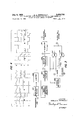
- FIGURE 1 is a block diagram of a binary transmitter unit in accordance with one embodiment of the present invention.
- FIGURE 2 shows various waveforms helpful in understanding the invention as shown and described in FIG- URE l;
- FIGURE 3 is a block diagram of a binary receiver in accordance with the first embodiment of the invention.
- FIGURE 4 shows various waveforms helpful in understanding the binary receiver shown and described in FIGURE 3;
- FIGURE 5 is a block diagram of a binary transmitter in accordance with a second embodiment of the present invention.
- FIGURE 6 is a block diagram of a four-level transmitter in accordance with the third embodiment of the present invention.
- FIGURE 7 shows various waveforms helpful in understanding the transmitter shown and described in FIG- URE 6.
- FIGURE 1 there is shown a block diagram of the binary transmitter according to one aspect of the present invention.
- Two carriers in a frequency ratio of f f are generated by frequency generators 101 and 103. These frequencies are selected for transmission by AND gates 107 and 109 according to whether the input data is mark (positive in this case) or space (zero m this case). The lower frequency, f is assigned to the mark state.
- a pulse is generated from each positive going transition of the combined carrier signal at the output of gates 107 and 109 to clock the data out of the information source 117 whether it be a facsimile scanner, electronic computer, or the like.
- This clock signal is thus at a dual rate according to whether the data being transmitted comprises marks or spaces. This precludes transmission of a serial stream of data arriving under control of an external clock unless intermediate storage is supplied.
- FIGURE shows a typical waveform comprising marks and spaces as the output of data from bufier store 115.
- the output from the buffer store 115 will assume either the mark or space level according to the state of the data at the output stage of the buffer store. If the mark level occurs as in FIGURE 20, AND gate 107 is enabled and the lower frequency f from frequency generator 101 is transmitted. This is seen in FIGURE 211. As soon as one cycle has occurred, another clock pulse is generated at pulse generator 111.
- FIGURE 2b shows the time relationship of the space frequency data.
- the output from inverter 105 is shown at FIGURE 2d, which is the data information inverted.
- FIGURE 2e shows the pulses generated at pulse generator 111 between the mark and space data.
- FIGURE 1 shows the generation and control of the carriers on a square wave basis. Therefore, a bandpass filter 113 is used at the output of the circuit to remove the unwanted high frequencies and thus transmit the carriers as fundamental sine waves.
- the inputs and outputs of the bandpass filter 113 are seen as FIGURES 2 and 2g, respectively.
- Phase continuity must be preserved at every data transition in order to insure that a clock pulse occurs at the end of each baud and also to avoid distortion of the baud, which would result from transmitting the phase discontinuity through a band limited channel.
- Phase continuity is guaranteed by using frequency sources designed to start in the same predetermined phase when turned on. This can be accomplished, for example, with clamped sine wave oscillators or with high frequency oscillators divided down to the desired frequency by resettable counter chains.
- a receiver for detecting the accelerated frequency shift keyed signal is shown in FIGURE 3.
- the bandpass filter 301, limiter 303, zero crossing detector 305, post detection filter 307, timing recovery 313, and sampling circuits 311 are all elements of a conventional frequency shift keyed synchronous demodulator. However, the timing recovery requirements are slightly different than in a conventional demodulator. If raw facsimile information containing long lengths of data with no transitions is being transmitted, start-stop timing utilizing local stable clocks may be appropriate. Transitions of the transmitted signal could be used directly for timing if the transmission medium is free of frequency shift. If the data rates are integrally related, the higher rate could be recovered by a phase locked loop operating from the recovered data envelope transitions, and divided down to obtain the lower rate.
- the data decision threshold is used for this purpose, i.e., when the marks are being received, the lower rate is selected for reclocking the data and when spaces are being received the higher rate is selected for reclocking the data.
- the fact that this reclocking technique produces marks of different time duration and spaces of different time duration is immaterial. Only their number is important at this point and the recovered clock guarantees that this information is available. If desired, the reclocking can be arranged so that this variation in time duration does not occur.
- the potential improvement in binary transmission speed for a block of data can be derived as follows. Let the improvement factor, or time compression be defined at the ratio of the normal transmission time, T, to the improved transmission time,
- the improvement factor is therefore T N n 1 1 Pi+Pi 2 This result shows that the improvement factor depends only on the ratio of the carriers and the fraction of the total data sent via the lower and upper carriers. Merely lowering f to reduce the ratio f /f does not result in a net increase in data rate.
- the waveform comprising one cycle of each of the marks and spaces, as shown in FIGURE 4/1, is seen to have entered the bandpass filter 301 from the transmission lines.
- the detected waveform of information after demodulation in the limiter 303, zero crossing detector 305, and post detection filter 307 as is known in the art is seen at FIGURE 42'.
- the decision threshold 309 which could be a squaring amplifier and limiter circuit, for example, returns the input information to its squarewave configuration, seen in FIGURE 4 and the output thereof in FIGURE 3.
- the output from the decision threshold 309 is then applied to the input of the timing recovery unit 313, AND gate 317, AND gate 319 via inverter 315, and sampler 311.
- the timing recovery unit 313 generates clock pulses at the f and the f rate in response to the mark and space pulses at the output of decision threshold 309.
- the f clock indicative of a mark pulse is seen at FIGURE 4k.
- the f clock, indicative of space pulse information, is seen in FIGURE 4m.
- These clock frequencies are then applied to the input to AND gates 317 and 319, which have been enabled by the application of the waveform from the decision threshold 309, seen in FIG- URE 4 while AND gate 319 receives the inverted wave form in FIGURE 4 as FIGURE 4k.
- the output from AND gates 317 and 319, seen at FIGURE 40 is the combined waveforms of FIGURE 4k and in, now utilized as a clock source to the receiver buifer unit, which is similar to that in the transmitter in FIGURE 1.
- the output from AND gates 317 and 319 is also applied to sampler unit 311.
- This unit may comprise a flipflop circuit and associated AND gates for generation of the specific pulses as seen in FIGURE 4n.
- the output from sampler 311 is thus the reclocked data which is to be stored in the buffer store for subsequent utilization by a printout device such as a facsimile printer.
- a single carrier frequency source and associated logic may be employed to insure phase continuity at the data transitions.
- the two carrier frequencies are generated by a 2400 c.p.s. oscillator 501 and a divider circuit '503, both of conventional design, which divides the oscillator fre quency by two. These frequencies are selected for transmission by associated gates according to whether the input data is mark (positive in this case) or space (zero).
- the lower frequency, 1200 c.p.s. in this instance, is assigned to the mark state.
- a pulse is generated from each positive going transition 'of the combined carrier signal at pulse generator 525. These pulses are used to clock the data out of the buffer store, not shown.
- the data line from the buffer storage unit will assume either the mark or space level according to the state of the data information. If the mark level occurs, the lower frequency (1200 c.p.s. in this case) is transmitted. As soon as a cycle has occurred, another clock pulse is generated. If the data is again mark, another cycle of 1200 c.p.s. is transmitted. If the data is space, the upper frequency (2400 c.p.s. in this case) is transmitted. As soon as a full cycle has occurred, another clock pulse is generated, and so on.
- the input data from the buffer store appears as an input to gates 509, 511, 517, 519 and via inverter 521 to gate 523.
- the outputs from the 2400 c.p.s. generator 501 and its associated divider network 503 appears as inputs to AND gate 505.
- AND gate 505 is enabled and, depending upon the data state of the input information, effectively enables either gate 511 or gate 509 via inverter 507. If the incoming binary digit at one particular time interval is a mark, then AND gate 511 is enabled, setting flipflop 513.
- flip-flop 513 would be reset.
- the set or 1 output from flip-flop 513 enables AND gate 519.
- the reset output from flip-flop 513 enables gate 517, which allows the inverse of the 1200' c.p.s. signal to appear on the output of AND gate 517.
- the other output from 2400 c.p.s. generator 501 is an input to AND gate 523.
- the data from the buffer store is inverted in phase by inverter 521 and appears as the other input to AND gate 523.
- Bandpass filter 527 is provided in a similar manner as was bandpass filter 113 in FIGURE 1 to filter out the unwanted harmonics of the square wave signals generated internally in the circuitry.
- the transition from the lower to higher frequency is always in-phase, but the transition from the higher to the lower frequency may be in phase or out-of-phase, depending upon how many cycles (bands) have occurred.
- the solution is to make both phases of the lower frequency available and to provide logic to select the proper phase.
- a transition from 2400 to 1200 c.p.s. Since the clock pulse is always generated at the output of pulse generator 525 from the positive going transition of the transmitted signal, the 2400 c.p.s. carrier is always positive (or I) immediately thereafter.
- the 1200 c.p.s. carrier may be either 1 or 0 at this time and the data may be either 1 or 0 (i.e., a mark or space) at this time. If the data is a space then the 2400 c.p.s. signal is to continue; there is no transition and therefore no phase problem.
- the data is a mark, then a transition is necessary, as the 2400 c.p.s. carrier is associated with space data. If the 2400 c.p.s. and 1200 c.p.s. signals are not of the same phase at this time, then the inverse of the 1200 c.p.s. frequency is selected as indicated by the logic table shown below. If the two signals are in phase then the normal 1200 c.p.s. signal is selected. Phase continuity isthus assured regardless of when transitions occur.
- FIGURE 6 there is shown a quaternary transmitter in accordance with a third aspect of the present invention.
- FIGURE 6 discloses frequency generators 701, 703, 705, and 707, which generate frequencies through 1, respectively.
- AND gates 709, 711, 713 and 715 are selectively enabled to allow the one cycle of the specific frequency to pass to the bandpass filter 719 and the pulse generator 717.
- the output from the pulse generator 717 is used to clock the information from a buffer store, not shown, in which the data information is intermediately stored upon output from the information source before being fed to the frequency generators and associated AND gates.
- the quaternary data inputs to AND gates 709, 711, 713 and 715 can be seen as curves p, q, r, and s, respectively.
- the outputs from the AND gates is shown in FIGURE 7a, showing the one cycle of each frequency enabled by the input data levels.
- the output from pulse generator 717 is shown as curve 1, which is used to clock the data from the buffer store to the frequency generators.
- Bandpass filter 719 is provided as were the bandpass filters in FIGURES 1 and 5, the output of which is curve v, to filter the unwanted harmonic frequencies occurring as a result of the square Wave signals shown in curve u in FIGURE 7.
- the speed improvement of the above embodiment depends upon the relative amount of time each level is transmitted. The most improvement occurs when the highest frequency is transmitted more often.
- the disclosed invention is particularly adaptable to black and white facsimile transmission.
- the invention could be used to transmit unencoded black and white facsimile images at an average rate higher than via an equivalent conventional frequency shift data system.
- One method is to utilize a constant velocity horizontal scan and a stepped vertical scan.
- the electrical signal produced by thehorizontal scan is quantized into binary digits and loaded into a binary data buffer store.
- the transmitter extracts the data from the buffer store and transmits it, according to the invention as was hereinbefore described.
- a control signal causes the scan to step vertically to the next line and the process continues.
- Various ways of optimizing the use of storage under such conditions are available.
- the receiver loads a bit store at a variable rate. When a complete line of data is available, control signals unload the data from the buffer store to the printer and advance it to the next line.
- Another method of transmitting black and White facsimile information is to utilize a scanning beam at both scanner and printer which can be positioned in discrete steps both horizontally and vertically.
- the beam is moved horizontally at two different rates, depending on whether black or white is being scanned, i.e., depending on which carrier frequency is being transmitted. In effect, therefore, the signal is quantized in a horizontal direction just as when storage is used.
- the process is reversed so that the printer scan is synchronized to the scanner.
- the invention is also adaptable to gray scale facsimile transmission. That is, if the modulator output frequency is a linear function of the input signal amplitude, scanning beam position can be controlled according to the number of crossovers of the output signal or the beam velocity can be controlled according to the output of a wide band discriminator used to detect the instantaneous frequency of the'output signal.
- the process is reversed so that the printer scan is positioned according to the number of crossovers received, if no carrier shift occurs in transmission, or the scan velocity is controlled by the receiver discriminator output.
- a method of transmitting signals representative of information from a data source comprising:
- step of transmitting includes:
- a data transmitter comprising:
- information source means for generating data signals of at least two information levels
- frequency generator means for generating a predetermined frequency signal for each information level of said data signals
- gating means coupled to said frequency generating means for transmitting one cycle of the selected frequency signals in response to the respective levels of said data signals;
- pulse generating means coupled to said gating means for generating clock pulses in response to each transmitted frequency signal and means coupling said pulse generating means to said information source to advance the data signals from said data source thereby allowing only said one cycle of said selected frequency signal to be transmitted.
- a device as set forth in claim 3 further including:
- buffer storage means coupled to said information source means for storing said data signals
- said buffer storage means being coupled to said pulse generating means and said gating means for emitting said stored data signals to said gating means in response to the clock pulse rate.
- a device as set forth in claim 4 further including:
- bandpass filter means for filtering out the undesirable harmonic frequencies in said transmitted frequency signals.
- a plurality of frequency generating means for generating a plurality of signals of predetermined frequencres
- gating means coupled to said plurality of frequency generating means operable to transmit one cycle of selected ones of said frequency signals in response to said data signals;
- pulse generating means coupled to said gating means for generating clock pulses in response to each cycle of the selected ones of said frequency signals
- a transmitter comprising:
- gating means coupled to said waveform generators operably controlled by said data signals to transmit selected ones of said waveforms
- a method of transmitting signals representative of information from a data source comprising:
- a data transmitter comprising:
- information source means for generating data signals of at least two information levels
- frequency generating means for generating a signal of predetermined frequency
- divider means responsive to said frequency generating means for generating at least one signal of a sub-multiple of said predetermined frequency
- first gating means coupled to said frequency generating means and said divider means, said first gating means being enabled at the coincidence of the phases of the predetermined frequency and the sub-multiple frequency;
- second gating means coupled to said first gating means and said information source means for emitting a first signal when said data signal is at a first information level and for emitting a second signal when said data signal is at a second information level;
- switching means coupled to said second gating means and operable to switch to a first or second state signal in response to said first and second signals, respectively;
- third gating means coupled to said first state output of said switching means for transmitting one cycle of said sub-multiple frequency in response to the coincidence of said first state signal, said sub-multiple frequency and said data signal level representative thereof;
- fourth gating means coupled to said second state output of said twitching means for transmitting one cycle of the opposite phase of said sub-multiple frequency in response to the coincidence of said second state signal, said sub-multiple frequency and said other data signal level representative thereof;
- fifth gating means for transmitting one cycle of said predetermined frequency in response to the coincidence of said signal of predetermined frequency and the opposite phase of said data signal
- pulse generating means coupled to said third, fourth, and fifth gating means for generating clock pulses in response to each transmitted frequency signal
Description
July 8, 1969 D. A. PERREAULT FSK TRANSMITTER WITH TRANSMISSION OF THE SAME NUMBER OF CYCLES OF EACH CARRIER FREQUENCY Sheet Filed Oct. 3. 1966 5.3 T r g umohm mwnEDm INVENTOR. DONALD A. PERREAULT A TTOR/VEY July 8, 1969 D. A.PERREAULT 'FSK TRANSMITTER WITH TRANSMISSION OF THE SAME NUMBER OF CYCLES OF EACH CARRIER FREQUENCY Filed Oct. 3. 1966 Sheet & of 4 mmOPm omxu umm OP XUOJU T L Y m at R M E m m V630 N w mm m 3 WM M mm ouwm 1 zoo-6C A W D 2? L W/ m D Wm 55:. mopoukmc njozmmmi 25 c 29280 fimwm o omwm 3Q 8Q 2 55:. m2: 5.524 oz m zQmmimz E 3? B? y 1969 1 D. A. PERREAULT 3,
FSK TRANSMITTER WITH TRANSMISSION OF THE SAME NUMBER OF CYCLES OF EACH CARRIER FREQUENCY Filed 001;. s. 1966 Sheet 5 of 4 TRANS- M ISSION LINE BAN DPASS F l LTER 8 a Q g mlo \014 o 40: t u :H-
l\ R n "5 F fi I M R] O M Q o m J 2 Q o ww 25 a g: o o On; I- QZ Nu 2 X F 8 0: .I on. o
INVENTOR.
DONALD A. PERREAULT 4&4 MM,
ATTORNE Y D. A. PERREAULT TH TRA July 8 1969 3.454,7l8 UMBER OF She et 4 FSK TRANSMITTER WI NSMISSION OF THE SAME N CYCLES OF EACH CARRIER FREQUENCY Filed 061;. 5, 1966 Y 653%. M N 55 mok mmzww 1H 1 N u 3.51 92 moimwzww 553mm. \R H 5 WE d5: C
v medmwzmw m w m R v m WP A 4 D N .L A W D B mD mJ (P40 ATTORNEY v United States Patent M 3,454,718 FSK TRANSMITTER WITH TRANSMISSION OF THE SAME NUMBER OF CYCLES OF EACH CARRIER FREQUENCY Donald A. Perreault, Pittsford, N.Y., assignor to Xerox Corporation, Rochester, N.Y., a corporation of New York Filed Oct. 3, 1966, Ser. No. 583,914 Int. Cl. H041 27/20, 27/12; H04n 5/38 US. Cl. 178-66 9 Claims ABSTRACT OF THE DISCLOSURE This invention relates to data transmission and, more particularly, to the transmission of digital data by frequency shift keying.
In the transmission of data information, as from a facsimile scanner or the output of a computer, it is often desired to transmit such information over switched telephone networks in order to utilize the extensive coverage of the switched telephone network and the relatively easy access to such networks that is available. In such transmission systems, quick and accurate service, however, as well as low cost operation, is desirable. To achieve low cost but rapid transmission service has, in the past, been difficult as the system required a large bandwidth capability transmission medium in order to maintain picture resolution and/or signal quality at a high level. The main drawback, therefore, to such prior art devices has been the prohibitively high rental or installation costs of the use of the transmission medium used to transmit the large signal densities. It is apparent, therefore, that the high cost of such transmission line service becomes a serious limitation on the economic usefulness of the facsimile or computer transmission equipment. The worldwide telephone network, therefore, provides an attractive means for transmitting graphic information with the attendant relatively low cost, extensive subscriber service, and the fact that no other transmission medium need be installed.
Transmission over the switched telephone network could be accomplished by the technique known as frea quency shift keying. Binary data transmission by frequency shift keying is accomplished by assigning a different carrier frequency to each state of the data, i.e., mark and space, and transmitting the appropriate frequency for a period of time sufiicient to insure reliable detection.
This is called a baud and its reciprocal is called the baud rate. In binary data transmission, each band carries one bit of information. Therefore, the baud rate is the same as the bit rate. In frequency shift key systems a limitation on the baud rate is the ratio of baud rate to the lower carrier frequency. In practical systems the ratio is usually one or greater, although systems with a ratio between A2 and 1 are known. In cases where the choice of the lower carrier is restricted by the channel, e.g. a voice frequency channel, this becomes the determining factor for the maximum baud rate which can be realized.
The frequency shift keying technique may be extended to include frequency transmission of data information with more than the normal two-level mark and space frequencies. That is, in a multi-level data transmission systern employing frequency shift keying, a plurality of fre- Patented July 8, 1969 quencies would be transmitted, one frequency for each level in the data waveform. With the lowest carrier frequency determining the upper limit on the baud rate, information transmission is even more critically hampered in a limited bandwidth transmission system.
It is accordingly, an object of the present invention to increase the efficiency of a data transmission system utilizing frequency shift keying.
It is another object of the present invention to optimize the information handling capability of graphic communication systems utilizing frequency shift keying.
It is another object of the present invention to reduce the operating costs of transmitting binary data information over a limited bandwidth transmission medium.
It is another object of the present invention to increase the baud rate of binary information transmission in frequency shift keyed graphic communication systems.
In accomplishing the above and other desired aspects, applicant has invented novel apparatus for efficiently transmitting graphic information to remote locations utilizing an improved frequency shift keyed transmitting system. Circuit means are provided for transmitting the same number of cycles, at least one, of each carrier frequency for each data state being transmitted. Thus, the baud length will depend upon which data state is being transmitted. The band will be shorter when the upper carrier is being transmitted than when the lower carrier is being transmitted, thus resulting in a higher average baud rate, except in cases where the data state is associated with the lower frequency predominates. In the ordinary facsimile system, for example, the black or data information (often five to ten percent of an average business document) would be associated with the lower carrier frequency, and the white or background (ninety to ninety-five percent of a document) would be associated with the upper frequency, thus producing a significant increase in document transmission rate. It is required, however, that the variable baud lengths of data be acquired under command of the transmitter, as, for example, from digital storage, from 'a computer, or from a facsimile scanner whose scanning beam position is under control of the transmitter. Likewise, the data must be delivered under command of the receiver to digital storage, or to a printout device as for a computer, or to a facsimile receiver whose scanning beam position is under control of the receiver.
For a more complete understanding of the invention, as well as other objects and further features thereof, reference may be had to the following detailed description in conjunction with the drawings wherein:
FIGURE 1 is a block diagram of a binary transmitter unit in accordance with one embodiment of the present invention;
FIGURE 2 shows various waveforms helpful in understanding the invention as shown and described in FIG- URE l;
FIGURE 3 is a block diagram of a binary receiver in accordance with the first embodiment of the invention;
FIGURE 4 shows various waveforms helpful in understanding the binary receiver shown and described in FIGURE 3;
FIGURE 5 is a block diagram of a binary transmitter in accordance with a second embodiment of the present invention;
FIGURE 6 is a block diagram of a four-level transmitter in accordance with the third embodiment of the present invention; and
FIGURE 7 shows various waveforms helpful in understanding the transmitter shown and described in FIG- URE 6.
Referring now to FIGURE 1, there is shown a block diagram of the binary transmitter according to one aspect of the present invention. Two carriers in a frequency ratio of f f are generated by frequency generators 101 and 103. These frequencies are selected for transmission by AND gates 107 and 109 according to whether the input data is mark (positive in this case) or space (zero m this case). The lower frequency, f is assigned to the mark state.
In order to provide that the input data state lasts for exactly one cycle of carrier (regardless of frequency), a pulse is generated from each positive going transition of the combined carrier signal at the output of gates 107 and 109 to clock the data out of the information source 117 whether it be a facsimile scanner, electronic computer, or the like. This clock signal is thus at a dual rate according to whether the data being transmitted comprises marks or spaces. This precludes transmission of a serial stream of data arriving under control of an external clock unless intermediate storage is supplied.
In operation, therefore, the data from the primary information source would be stored intermediately at a buffer store 115, of conventional design, in order to provide an immediate, continuous output of information independent of the rate at which the information source 117 generates the binary information. FIGURE shows a typical waveform comprising marks and spaces as the output of data from bufier store 115. When a clock pulse from pulse generator 111 occurs, the output from the buffer store 115 will assume either the mark or space level according to the state of the data at the output stage of the buffer store. If the mark level occurs as in FIGURE 20, AND gate 107 is enabled and the lower frequency f from frequency generator 101 is transmitted. This is seen in FIGURE 211. As soon as one cycle has occurred, another clock pulse is generated at pulse generator 111. If the data is again mark another cycle of f is transmitted. If the input data is a space, AND gate 109 is enabled via inverter 105 and the upper frequency f from frequency generator 103 is generated, and so on. FIGURE 2b shows the time relationship of the space frequency data. The output from inverter 105 is shown at FIGURE 2d, which is the data information inverted. FIGURE 2e shows the pulses generated at pulse generator 111 between the mark and space data. FIGURE 1 shows the generation and control of the carriers on a square wave basis. Therefore, a bandpass filter 113 is used at the output of the circuit to remove the unwanted high frequencies and thus transmit the carriers as fundamental sine waves. The inputs and outputs of the bandpass filter 113 are seen as FIGURES 2 and 2g, respectively.
Phase continuity must be preserved at every data transition in order to insure that a clock pulse occurs at the end of each baud and also to avoid distortion of the baud, which would result from transmitting the phase discontinuity through a band limited channel. Phase continuity is guaranteed by using frequency sources designed to start in the same predetermined phase when turned on. This can be accomplished, for example, with clamped sine wave oscillators or with high frequency oscillators divided down to the desired frequency by resettable counter chains.
A receiver for detecting the accelerated frequency shift keyed signal is shown in FIGURE 3. The bandpass filter 301, limiter 303, zero crossing detector 305, post detection filter 307, timing recovery 313, and sampling circuits 311 are all elements of a conventional frequency shift keyed synchronous demodulator. However, the timing recovery requirements are slightly different than in a conventional demodulator. If raw facsimile information containing long lengths of data with no transitions is being transmitted, start-stop timing utilizing local stable clocks may be appropriate. Transitions of the transmitted signal could be used directly for timing if the transmission medium is free of frequency shift. If the data rates are integrally related, the higher rate could be recovered by a phase locked loop operating from the recovered data envelope transitions, and divided down to obtain the lower rate. In any case, it is essential that both data rates be available for reclocking the data and that means be provided for selecting the appropriate rate. In FIGURE 2, the data decision threshold is used for this purpose, i.e., when the marks are being received, the lower rate is selected for reclocking the data and when spaces are being received the higher rate is selected for reclocking the data. The fact that this reclocking technique produces marks of different time duration and spaces of different time duration is immaterial. Only their number is important at this point and the recovered clock guarantees that this information is available. If desired, the reclocking can be arranged so that this variation in time duration does not occur.
The potential improvement in binary transmission speed for a block of data, a facsimile document for example, can be derived as follows. Let the improvement factor, or time compression be defined at the ratio of the normal transmission time, T, to the improved transmission time,
If the normal data rate is based on the lower carrier frequency, as is usually the case, the normal transmission time is where =total number of bits to be transmitted. n=number of cycles of lower carrier per baud. f =lower carrier frequency.
The improved transmission time is given by where,
P =fraction of a block sent via f P fraction of a block sent via f f =lower carrier frequency. f =upper carrier frequency.
The improvement factor is therefore T N n 1 1 Pi+Pi 2 This result shows that the improvement factor depends only on the ratio of the carriers and the fraction of the total data sent via the lower and upper carriers. Merely lowering f to reduce the ratio f /f does not result in a net increase in data rate.
In operation, the waveform comprising one cycle of each of the marks and spaces, as shown in FIGURE 4/1, is seen to have entered the bandpass filter 301 from the transmission lines. The detected waveform of information after demodulation in the limiter 303, zero crossing detector 305, and post detection filter 307 as is known in the art is seen at FIGURE 42'.
The decision threshold 309, which could be a squaring amplifier and limiter circuit, for example, returns the input information to its squarewave configuration, seen in FIGURE 4 and the output thereof in FIGURE 3.
The output from the decision threshold 309 is then applied to the input of the timing recovery unit 313, AND gate 317, AND gate 319 via inverter 315, and sampler 311. The timing recovery unit 313 generates clock pulses at the f and the f rate in response to the mark and space pulses at the output of decision threshold 309. The f clock indicative of a mark pulse is seen at FIGURE 4k. The f clock, indicative of space pulse information, is seen in FIGURE 4m. These clock frequencies are then applied to the input to AND gates 317 and 319, which have been enabled by the application of the waveform from the decision threshold 309, seen in FIG- URE 4 while AND gate 319 receives the inverted wave form in FIGURE 4 as FIGURE 4k. The output from AND gates 317 and 319, seen at FIGURE 40, is the combined waveforms of FIGURE 4k and in, now utilized as a clock source to the receiver buifer unit, which is similar to that in the transmitter in FIGURE 1.
The output from AND gates 317 and 319 is also applied to sampler unit 311. This unit may comprise a flipflop circuit and associated AND gates for generation of the specific pulses as seen in FIGURE 4n. The output from sampler 311 is thus the reclocked data which is to be stored in the buffer store for subsequent utilization by a printout device such as a facsimile printer.
In accordance with the second aspect of the present invention, as seen in FIGURE 5, if the carrier frequencies are integrally related, a single carrier frequency source and associated logic may be employed to insure phase continuity at the data transitions.
The two carrier frequencies are generated by a 2400 c.p.s. oscillator 501 and a divider circuit '503, both of conventional design, which divides the oscillator fre quency by two. These frequencies are selected for transmission by associated gates according to whether the input data is mark (positive in this case) or space (zero). The lower frequency, 1200 c.p.s. in this instance, is assigned to the mark state. In order to provide that the input data state lasts for exactly one cycle of carrier, regardless of frequency, in accordance with the principles of the present invention, a pulse is generated from each positive going transition 'of the combined carrier signal at pulse generator 525. These pulses are used to clock the data out of the buffer store, not shown. When a clock pulse occurs, the data line from the buffer storage unit will assume either the mark or space level according to the state of the data information. If the mark level occurs, the lower frequency (1200 c.p.s. in this case) is transmitted. As soon as a cycle has occurred, another clock pulse is generated. If the data is again mark, another cycle of 1200 c.p.s. is transmitted. If the data is space, the upper frequency (2400 c.p.s. in this case) is transmitted. As soon as a full cycle has occurred, another clock pulse is generated, and so on.
In operation of the embodiment shown in FIGURE 5, the input data from the buffer store appears as an input to gates 509, 511, 517, 519 and via inverter 521 to gate 523. The outputs from the 2400 c.p.s. generator 501 and its associated divider network 503 appears as inputs to AND gate 505. At the coincidence of the phases of the two frequencies, AND gate 505 is enabled and, depending upon the data state of the input information, effectively enables either gate 511 or gate 509 via inverter 507. If the incoming binary digit at one particular time interval is a mark, then AND gate 511 is enabled, setting flipflop 513.
If the binary data happened to be a space then flip-flop 513 would be reset. The set or 1 output from flip-flop 513 enables AND gate 519. With the other two inputs to the gate 519 being the data and the 1200 c.p.s. signal, one cycle at the 1200 c.p.s. rate would be passed out to the bandpass filter 527. In a similar manner, the reset output from flip-flop 513 enables gate 517, which allows the inverse of the 1200' c.p.s. signal to appear on the output of AND gate 517. The other output from 2400 c.p.s. generator 501 is an input to AND gate 523. The data from the buffer store is inverted in phase by inverter 521 and appears as the other input to AND gate 523. Thus, at the particular phase indication, the output from the gates 517, 519 and 523 are the proper frequencies, i.e.,
1200 or 2400 c.p.s., which allows the pulse generator 525 to generate the clock pulse in a manner to be described. Bandpass filter 527 is provided in a similar manner as was bandpass filter 113 in FIGURE 1 to filter out the unwanted harmonics of the square wave signals generated internally in the circuitry.
In the above example, the transition from the lower to higher frequency is always in-phase, but the transition from the higher to the lower frequency may be in phase or out-of-phase, depending upon how many cycles (bands) have occurred. The solution is to make both phases of the lower frequency available and to provide logic to select the proper phase. Consider, for example, a transition from 2400 to 1200 c.p.s. Since the clock pulse is always generated at the output of pulse generator 525 from the positive going transition of the transmitted signal, the 2400 c.p.s. carrier is always positive (or I) immediately thereafter. The 1200 c.p.s. carrier may be either 1 or 0 at this time and the data may be either 1 or 0 (i.e., a mark or space) at this time. If the data is a space then the 2400 c.p.s. signal is to continue; there is no transition and therefore no phase problem.
If the data is a mark, then a transition is necessary, as the 2400 c.p.s. carrier is associated with space data. If the 2400 c.p.s. and 1200 c.p.s. signals are not of the same phase at this time, then the inverse of the 1200 c.p.s. frequency is selected as indicated by the logic table shown below. If the two signals are in phase then the normal 1200 c.p.s. signal is selected. Phase continuity isthus assured regardless of when transitions occur.
LOGIC TABLE FOR TRANSMITTER OF FIG. 5 [Last bit-space] 1,200 carrier AND gate 517, AND gate 519- AND gate 523 O utput 1 Inverted. 2 Normal.
Referring now to FIGURE 6, there is shown a quaternary transmitter in accordance with a third aspect of the present invention. In a frequency shift keyed signal utilizing more than two frequencies, separate carrier sources must ordinarily be utilized unless a very fortuitous spacing of carrier frequencies is available. FIGURE 6 discloses frequency generators 701, 703, 705, and 707, which generate frequencies through 1, respectively. With each incoming level representative of information data, AND gates 709, 711, 713 and 715 are selectively enabled to allow the one cycle of the specific frequency to pass to the bandpass filter 719 and the pulse generator 717. The output from the pulse generator 717 is used to clock the information from a buffer store, not shown, in which the data information is intermediately stored upon output from the information source before being fed to the frequency generators and associated AND gates.
With reference to FIGURE 7, the quaternary data inputs to AND gates 709, 711, 713 and 715 can be seen as curves p, q, r, and s, respectively. The outputs from the AND gates is shown in FIGURE 7a, showing the one cycle of each frequency enabled by the input data levels. The output from pulse generator 717 is shown as curve 1, which is used to clock the data from the buffer store to the frequency generators. Bandpass filter 719 is provided as were the bandpass filters in FIGURES 1 and 5, the output of which is curve v, to filter the unwanted harmonic frequencies occurring as a result of the square Wave signals shown in curve u in FIGURE 7.
The speed improvement of the above embodiment depends upon the relative amount of time each level is transmitted. The most improvement occurs when the highest frequency is transmitted more often. The improvement factor is given by the expression th a where f1, f f f =carrier frequencies.
For example, if P =P =P =P as for well encoded data, and f =120O, f =1600, f =2O0O, f =2400, as for a possible voice frequency data system, then C=1.4, indicating an average baud rate of 1680 instead of 1200, or an average bit rate of 3360, instead of 2400, if the data is Nyquist encoded.
The disclosed invention is particularly adaptable to black and white facsimile transmission. The invention could be used to transmit unencoded black and white facsimile images at an average rate higher than via an equivalent conventional frequency shift data system. One method is to utilize a constant velocity horizontal scan and a stepped vertical scan. The electrical signal produced by thehorizontal scan is quantized into binary digits and loaded into a binary data buffer store. The transmitter extracts the data from the buffer store and transmits it, according to the invention as was hereinbefore described. When the buffer store is empty a control signal causes the scan to step vertically to the next line and the process continues. Various ways of optimizing the use of storage under such conditions are available. At the printer, the receiver loads a bit store at a variable rate. When a complete line of data is available, control signals unload the data from the buffer store to the printer and advance it to the next line.
Another method of transmitting black and White facsimile information is to utilize a scanning beam at both scanner and printer which can be positioned in discrete steps both horizontally and vertically. The beam is moved horizontally at two different rates, depending on whether black or white is being scanned, i.e., depending on which carrier frequency is being transmitted. In effect, therefore, the signal is quantized in a horizontal direction just as when storage is used. At the receiver-printer the process is reversed so that the printer scan is synchronized to the scanner.
The invention is also adaptable to gray scale facsimile transmission. That is, if the modulator output frequency is a linear function of the input signal amplitude, scanning beam position can be controlled according to the number of crossovers of the output signal or the beam velocity can be controlled according to the output of a wide band discriminator used to detect the instantaneous frequency of the'output signal. At the receiver-printer the process is reversed so that the printer scan is positioned according to the number of crossovers received, if no carrier shift occurs in transmission, or the scan velocity is controlled by the receiver discriminator output.
In the foregoing, there has been disclosed methods and apparatus for optimizing the transmission of binary signals in a frequency shift keyed system. While the different embodiments have been described with respect to a facsimile scanning system, such circuitry is exemplary only as other circuits and apparatus could be utilized in a frequency shift keyed system to perform the disclosed transmit and receive functions. In addition, certain binary transmission rates and frequency modulated signals are disclosed, but it is apparent that other rates and frequencies could be used within the scope of the invention.
Thus, while the present invention, as to its objects and advantages, as described herein, has been set forth in specific embodiments thereof, they are to be understood as illustrative only and not limiting.
What is claimed is:
1. A method of transmitting signals representative of information from a data source comprising:
generating a predetermined frequency signal for each level of information emanating from said data source; and
transmitting one cycle of each frequency signal in response to the respective level of information from said data source.
2. The method as set forth in claim 1, wherein said step of transmitting includes:
gating each of said frequency signals in response to the respective level of information from said data source; and
clocking said information data source at the rate which the frequency signals are gated whereby only one cycle of each frequency is transmitted.
3. A data transmitter comprising:
information source means for generating data signals of at least two information levels;
frequency generator means for generating a predetermined frequency signal for each information level of said data signals;
gating means coupled to said frequency generating means for transmitting one cycle of the selected frequency signals in response to the respective levels of said data signals;
pulse generating means coupled to said gating means for generating clock pulses in response to each transmitted frequency signal and means coupling said pulse generating means to said information source to advance the data signals from said data source thereby allowing only said one cycle of said selected frequency signal to be transmitted.
4. A device as set forth in claim 3 further including:
buffer storage means coupled to said information source means for storing said data signals;
said buffer storage means being coupled to said pulse generating means and said gating means for emitting said stored data signals to said gating means in response to the clock pulse rate.
5. A device as set forth in claim 4 further including:
bandpass filter means for filtering out the undesirable harmonic frequencies in said transmitted frequency signals.
6. In a frequency shift-key transmitter, the combination comprising:
a plurality of frequency generating means for generating a plurality of signals of predetermined frequencres;
a source of data signals;
gating means coupled to said plurality of frequency generating means operable to transmit one cycle of selected ones of said frequency signals in response to said data signals;
pulse generating means coupled to said gating means for generating clock pulses in response to each cycle of the selected ones of said frequency signals; and
means coupling said pulse generating means to said data signal source to advance data signals in a time relationship with said clock pulses, whereby only said one cycle of each of said frequency signals is transmitted.
7. In a data transmission system, a transmitter comprising:
a plurality of waveform generators, each having a different frequency of oscillation;
a source of data signals;
gating means coupled to said waveform generators operably controlled by said data signals to transmit selected ones of said waveforms; and
means coupled to said gating means for transmitting only one cycle of each of the selected ones of said waveforms.
8. A method of transmitting signals representative of information from a data source comprising:
generating a predetermined frequency signal for one level of information emanating from said data source;
dividing said predetermined frequency signal into a submultiple frequency signal for another level of information emanating from said data source;
transmitting one cycle of said frequency signal in response to the respective level of information from said data source;
further transmitting one cycle of one phase of said sub-multiple frequency signal in response to the respective level of information from said data source when the transition from the higher to sub-multiple frequency signal is in phase, and
further transmitting one cycle of the opposite phase of said sub-multiple frequency signal in response to the respective level of information from said data source when the transition from the higher to sub-multiple frequency signal is 180 out of phase.
9. A data transmitter comprising:
information source means for generating data signals of at least two information levels;
frequency generating means for generating a signal of predetermined frequency;
divider means responsive to said frequency generating means for generating at least one signal of a sub-multiple of said predetermined frequency;
first gating means coupled to said frequency generating means and said divider means, said first gating means being enabled at the coincidence of the phases of the predetermined frequency and the sub-multiple frequency;
second gating means coupled to said first gating means and said information source means for emitting a first signal when said data signal is at a first information level and for emitting a second signal when said data signal is at a second information level;
switching means coupled to said second gating means and operable to switch to a first or second state signal in response to said first and second signals, respectively;
third gating means coupled to said first state output of said switching means for transmitting one cycle of said sub-multiple frequency in response to the coincidence of said first state signal, said sub-multiple frequency and said data signal level representative thereof;
fourth gating means coupled to said second state output of said twitching means for transmitting one cycle of the opposite phase of said sub-multiple frequency in response to the coincidence of said second state signal, said sub-multiple frequency and said other data signal level representative thereof;
fifth gating means for transmitting one cycle of said predetermined frequency in response to the coincidence of said signal of predetermined frequency and the opposite phase of said data signal;
pulse generating means coupled to said third, fourth, and fifth gating means for generating clock pulses in response to each transmitted frequency signal, and
means coupling said pulse generating means to said information source to advance the said pulses utilized to step the data signals from said information source thereby allowing only said one cycle of each of said frequencies to be transmitted.
References Cited UNITED STATES PATENTS 3,102,238 8/1963 Bosen 32827 3,142,723 7/1964 Fleming 32530 X 3,165,583 1/1965 Kretzmer et a1. 178-66 3,190,958 6/1965 Bullwinkle et al. 325-30 X ROBERT L. GRIFFIN, Primary Examiner.
WILLIAM S. FROMMER, Assistant Examiner.
U.S. Cl. X.R.
Applications Claiming Priority (1)
| Application Number | Priority Date | Filing Date | Title |
|---|---|---|---|
| US58391466A | 1966-10-03 | 1966-10-03 |
Publications (1)
| Publication Number | Publication Date |
|---|---|
| US3454718A true US3454718A (en) | 1969-07-08 |
Family
ID=24335124
Family Applications (1)
| Application Number | Title | Priority Date | Filing Date |
|---|---|---|---|
| US583914A Expired - Lifetime US3454718A (en) | 1966-10-03 | 1966-10-03 | Fsk transmitter with transmission of the same number of cycles of each carrier frequency |
Country Status (1)
| Country | Link |
|---|---|
| US (1) | US3454718A (en) |
Cited By (81)
| Publication number | Priority date | Publication date | Assignee | Title |
|---|---|---|---|---|
| US3566033A (en) * | 1967-05-09 | 1971-02-23 | Serck Controls Ltd | Frequency shift signal transmission systems using half-cycles of frequency shift oscillator |
| US3611148A (en) * | 1965-04-15 | 1971-10-05 | Serck Controls Ltd | Data transmission system for binary coded data using single frequency shift oscillator |
| US3611209A (en) * | 1969-12-11 | 1971-10-05 | Bell Telephone Labor Inc | Digital filter frequency shift modulator |
| US3668562A (en) * | 1970-04-15 | 1972-06-06 | Tel Tech Corp | Frequency modulation system for transmitting binary information |
| US3689913A (en) * | 1970-04-17 | 1972-09-05 | Rca Corp | Conversion to a digital code which is self-clocking and absolute phasing |
| US3701053A (en) * | 1970-03-18 | 1972-10-24 | Acec | Process and apparatus for transmission of binary messages by synchronized frequency shift keying |
| US3737895A (en) * | 1971-08-02 | 1973-06-05 | Edmac Ass Inc | Bi-phase data recorder |
| US3747074A (en) * | 1972-03-17 | 1973-07-17 | Comteu | Method of and apparatus for baud rate detection |
| US3748398A (en) * | 1970-10-13 | 1973-07-24 | Licentia Gmbh | Circuit arrangement for determining the existence of a calling condition on channels of a multiplex radiotelephone communication system |
| US3779321A (en) * | 1972-06-30 | 1973-12-18 | Teletype Corp | Data transmitting systems |
| US3808533A (en) * | 1971-09-10 | 1974-04-30 | Us Navy | High volume, binary data transmission system |
| US3918085A (en) * | 1974-01-12 | 1975-11-04 | Sony Corp | Magnetic recording and/or reproducing apparatus |
| US3930121A (en) * | 1973-04-13 | 1975-12-30 | Int Standard Electric Corp | Method for converting a binary coded data signal into a P-FSK coded signal |
| US3932704A (en) * | 1970-08-19 | 1976-01-13 | Coherent Communications System Corporation | Coherent digital frequency shift keying system |
| JPS5228812A (en) * | 1975-08-29 | 1977-03-04 | Nippon Res & Syst:Kk | Data communication system |
| JPS5330203A (en) * | 1976-09-02 | 1978-03-22 | Tadashi Nishimura | Multiifrequency type data transmitter |
| US4090135A (en) * | 1976-06-29 | 1978-05-16 | The United States Of America As Represented By The Secretary Of The Interior | Wireless FSK technique for telemetering underground data to the surface |
| JPS5541065A (en) * | 1978-09-18 | 1980-03-22 | Nippon Telegr & Teleph Corp <Ntt> | Data transmitter |
| EP0093819A1 (en) * | 1982-04-29 | 1983-11-16 | Ascom Autophon Ag | System for the radio transmission of a binary coded signal |
| US4417349A (en) * | 1979-11-08 | 1983-11-22 | Digital Broadcasting Corporation | SCA Data transmission system with a raised cosine filter |
| FR2529042A1 (en) * | 1982-06-16 | 1983-12-23 | Alsthom Cgee | Coded signal data transmission system - uses two synthesisers to provide two frequencies for pulses combined with amplitude modulation |
| WO1985003609A1 (en) * | 1984-02-01 | 1985-08-15 | Webb Leon C | Zero crossing switching modulation systems and methods |
| US4564823A (en) * | 1984-09-24 | 1986-01-14 | Robot Research, Inc. | Fractional-cycle time/amplitude modulation |
| EP0172048A2 (en) * | 1984-06-19 | 1986-02-19 | Intersat Radio Communications Inc. | A method of transmitting digital data by modulating a high frequency signal |
| US4596022A (en) * | 1983-08-25 | 1986-06-17 | The Microperipheral Corporation | FSK data communication system |
| US4627078A (en) * | 1983-08-25 | 1986-12-02 | The Microperipheral Corporation | Data communication system |
| US4771440A (en) * | 1986-12-03 | 1988-09-13 | Cray Research, Inc. | Data modulation interface |
| US4926444A (en) * | 1988-04-29 | 1990-05-15 | Scientific-Atlanta, Inc. | Data transmission method and apparatus by period shift keying (TSK) |
| US4992748A (en) * | 1989-09-13 | 1991-02-12 | Atlantic Richfield Company | Period-inverting FM demodulator |
| US5105444A (en) * | 1989-09-13 | 1992-04-14 | Atlantic Richfield Company | System for high speed data tranmission |
| US5406584A (en) * | 1992-09-01 | 1995-04-11 | X-Com, Inc. | Time shift keying digital communications system |
| US5524121A (en) * | 1994-03-11 | 1996-06-04 | Smk Corporation | Digital data modulating method |
| US5724357A (en) * | 1992-01-28 | 1998-03-03 | Fleetwood Group, Inc. | Remote response system and data transfer protocol |
| US5748679A (en) * | 1995-04-28 | 1998-05-05 | Trw Inc. | Modulated clock MSK modulator for high data rate applications |
| US6021119A (en) * | 1994-06-24 | 2000-02-01 | Fleetwood Group, Inc. | Multiple site interactive response system |
| US6049706A (en) * | 1998-10-21 | 2000-04-11 | Parkervision, Inc. | Integrated frequency translation and selectivity |
| US6061555A (en) * | 1998-10-21 | 2000-05-09 | Parkervision, Inc. | Method and system for ensuring reception of a communications signal |
| US6061551A (en) * | 1998-10-21 | 2000-05-09 | Parkervision, Inc. | Method and system for down-converting electromagnetic signals |
| US6091940A (en) * | 1998-10-21 | 2000-07-18 | Parkervision, Inc. | Method and system for frequency up-conversion |
| US6370371B1 (en) | 1998-10-21 | 2002-04-09 | Parkervision, Inc. | Applications of universal frequency translation |
| US6542722B1 (en) | 1998-10-21 | 2003-04-01 | Parkervision, Inc. | Method and system for frequency up-conversion with variety of transmitter configurations |
| US6560301B1 (en) | 1998-10-21 | 2003-05-06 | Parkervision, Inc. | Integrated frequency translation and selectivity with a variety of filter embodiments |
| US20030128776A1 (en) * | 2001-11-09 | 2003-07-10 | Parkervision, Inc | Method and apparatus for reducing DC off sets in a communication system |
| US6694128B1 (en) | 1998-08-18 | 2004-02-17 | Parkervision, Inc. | Frequency synthesizer using universal frequency translation technology |
| US6704549B1 (en) | 1999-03-03 | 2004-03-09 | Parkvision, Inc. | Multi-mode, multi-band communication system |
| US6704558B1 (en) | 1999-01-22 | 2004-03-09 | Parkervision, Inc. | Image-reject down-converter and embodiments thereof, such as the family radio service |
| US20040196910A1 (en) * | 2003-01-27 | 2004-10-07 | Xg Technology, Llc | Integer cycle frequency hopping modulation for the radio frequency transmission of high speed data |
| US6813485B2 (en) | 1998-10-21 | 2004-11-02 | Parkervision, Inc. | Method and system for down-converting and up-converting an electromagnetic signal, and transforms for same |
| JP2004534421A (en) * | 1999-03-29 | 2004-11-11 | ユージン ジスキー | Method and apparatus for compressing analog and digital signals and data |
| US6873836B1 (en) | 1999-03-03 | 2005-03-29 | Parkervision, Inc. | Universal platform module and methods and apparatuses relating thereto enabled by universal frequency translation technology |
| US6879817B1 (en) | 1999-04-16 | 2005-04-12 | Parkervision, Inc. | DC offset, re-radiation, and I/Q solutions using universal frequency translation technology |
| US6963734B2 (en) | 1999-12-22 | 2005-11-08 | Parkervision, Inc. | Differential frequency down-conversion using techniques of universal frequency translation technology |
| US6975848B2 (en) | 2002-06-04 | 2005-12-13 | Parkervision, Inc. | Method and apparatus for DC offset removal in a radio frequency communication channel |
| US7006805B1 (en) | 1999-01-22 | 2006-02-28 | Parker Vision, Inc. | Aliasing communication system with multi-mode and multi-band functionality and embodiments thereof, such as the family radio service |
| US7010559B2 (en) | 2000-11-14 | 2006-03-07 | Parkervision, Inc. | Method and apparatus for a parallel correlator and applications thereof |
| US7010286B2 (en) | 2000-04-14 | 2006-03-07 | Parkervision, Inc. | Apparatus, system, and method for down-converting and up-converting electromagnetic signals |
| US7027786B1 (en) | 1998-10-21 | 2006-04-11 | Parkervision, Inc. | Carrier and clock recovery using universal frequency translation |
| EP1649656A2 (en) * | 2003-06-24 | 2006-04-26 | Xg Technology, Llc | Tri-state integer cycle modulation |
| US7039372B1 (en) | 1998-10-21 | 2006-05-02 | Parkervision, Inc. | Method and system for frequency up-conversion with modulation embodiments |
| US7054296B1 (en) | 1999-08-04 | 2006-05-30 | Parkervision, Inc. | Wireless local area network (WLAN) technology and applications including techniques of universal frequency translation |
| US7072390B1 (en) | 1999-08-04 | 2006-07-04 | Parkervision, Inc. | Wireless local area network (WLAN) using universal frequency translation technology including multi-phase embodiments |
| US7082171B1 (en) | 1999-11-24 | 2006-07-25 | Parkervision, Inc. | Phase shifting applications of universal frequency translation |
| US7085335B2 (en) | 2001-11-09 | 2006-08-01 | Parkervision, Inc. | Method and apparatus for reducing DC offsets in a communication system |
| US7110444B1 (en) | 1999-08-04 | 2006-09-19 | Parkervision, Inc. | Wireless local area network (WLAN) using universal frequency translation technology including multi-phase embodiments and circuit implementations |
| US7110435B1 (en) | 1999-03-15 | 2006-09-19 | Parkervision, Inc. | Spread spectrum applications of universal frequency translation |
| EP1757055A2 (en) * | 2004-06-04 | 2007-02-28 | Xg Technology, Llc | Integer cycle event detection using wavelet pass filter system and method |
| US7236754B2 (en) | 1999-08-23 | 2007-06-26 | Parkervision, Inc. | Method and system for frequency up-conversion |
| US7292835B2 (en) | 2000-01-28 | 2007-11-06 | Parkervision, Inc. | Wireless and wired cable modem applications of universal frequency translation technology |
| US7295826B1 (en) | 1998-10-21 | 2007-11-13 | Parkervision, Inc. | Integrated frequency translation and selectivity with gain control functionality, and applications thereof |
| US7321640B2 (en) | 2002-06-07 | 2008-01-22 | Parkervision, Inc. | Active polyphase inverter filter for quadrature signal generation |
| US7379883B2 (en) | 2002-07-18 | 2008-05-27 | Parkervision, Inc. | Networking methods and systems |
| US7454453B2 (en) | 2000-11-14 | 2008-11-18 | Parkervision, Inc. | Methods, systems, and computer program products for parallel correlation and applications thereof |
| US7460584B2 (en) | 2002-07-18 | 2008-12-02 | Parkervision, Inc. | Networking methods and systems |
| US7515896B1 (en) | 1998-10-21 | 2009-04-07 | Parkervision, Inc. | Method and system for down-converting an electromagnetic signal, and transforms for same, and aperture relationships |
| US7554508B2 (en) | 2000-06-09 | 2009-06-30 | Parker Vision, Inc. | Phased array antenna applications on universal frequency translation |
| US7693230B2 (en) | 1999-04-16 | 2010-04-06 | Parkervision, Inc. | Apparatus and method of differential IQ frequency up-conversion |
| US7724845B2 (en) | 1999-04-16 | 2010-05-25 | Parkervision, Inc. | Method and system for down-converting and electromagnetic signal, and transforms for same |
| US7773688B2 (en) | 1999-04-16 | 2010-08-10 | Parkervision, Inc. | Method, system, and apparatus for balanced frequency up-conversion, including circuitry to directly couple the outputs of multiple transistors |
| US20120250507A1 (en) * | 2011-03-30 | 2012-10-04 | International Business Machines Corporation | Device and method for adjusting rate limits for transmission rates of data flows having a certain priority in a transmitter |
| US8295406B1 (en) | 1999-08-04 | 2012-10-23 | Parkervision, Inc. | Universal platform module for a plurality of communication protocols |
| US20160134451A1 (en) * | 2012-12-27 | 2016-05-12 | Panasonic Corporation | Receiving apparatus and demodulation method |
Citations (4)
| Publication number | Priority date | Publication date | Assignee | Title |
|---|---|---|---|---|
| US3102238A (en) * | 1961-11-13 | 1963-08-27 | Collins Radio Co | Encoder with one frequency indicating one binary logic state and another frequency indicating other state |
| US3142723A (en) * | 1961-11-29 | 1964-07-28 | Bell Telephone Labor Inc | Frequency shift keying system |
| US3165583A (en) * | 1960-11-21 | 1965-01-12 | Bell Telephone Labor Inc | Two-tone transmission system for digital data |
| US3190958A (en) * | 1962-09-05 | 1965-06-22 | Edward C Bullwinkel | Frequency-shift-keyed signal generator with phase mismatch prevention means |
-
1966
- 1966-10-03 US US583914A patent/US3454718A/en not_active Expired - Lifetime
Patent Citations (4)
| Publication number | Priority date | Publication date | Assignee | Title |
|---|---|---|---|---|
| US3165583A (en) * | 1960-11-21 | 1965-01-12 | Bell Telephone Labor Inc | Two-tone transmission system for digital data |
| US3102238A (en) * | 1961-11-13 | 1963-08-27 | Collins Radio Co | Encoder with one frequency indicating one binary logic state and another frequency indicating other state |
| US3142723A (en) * | 1961-11-29 | 1964-07-28 | Bell Telephone Labor Inc | Frequency shift keying system |
| US3190958A (en) * | 1962-09-05 | 1965-06-22 | Edward C Bullwinkel | Frequency-shift-keyed signal generator with phase mismatch prevention means |
Cited By (155)
| Publication number | Priority date | Publication date | Assignee | Title |
|---|---|---|---|---|
| US3611148A (en) * | 1965-04-15 | 1971-10-05 | Serck Controls Ltd | Data transmission system for binary coded data using single frequency shift oscillator |
| US3566033A (en) * | 1967-05-09 | 1971-02-23 | Serck Controls Ltd | Frequency shift signal transmission systems using half-cycles of frequency shift oscillator |
| US3611209A (en) * | 1969-12-11 | 1971-10-05 | Bell Telephone Labor Inc | Digital filter frequency shift modulator |
| US3701053A (en) * | 1970-03-18 | 1972-10-24 | Acec | Process and apparatus for transmission of binary messages by synchronized frequency shift keying |
| US3668562A (en) * | 1970-04-15 | 1972-06-06 | Tel Tech Corp | Frequency modulation system for transmitting binary information |
| US3689913A (en) * | 1970-04-17 | 1972-09-05 | Rca Corp | Conversion to a digital code which is self-clocking and absolute phasing |
| US3932704A (en) * | 1970-08-19 | 1976-01-13 | Coherent Communications System Corporation | Coherent digital frequency shift keying system |
| US3748398A (en) * | 1970-10-13 | 1973-07-24 | Licentia Gmbh | Circuit arrangement for determining the existence of a calling condition on channels of a multiplex radiotelephone communication system |
| US3737895A (en) * | 1971-08-02 | 1973-06-05 | Edmac Ass Inc | Bi-phase data recorder |
| US3808533A (en) * | 1971-09-10 | 1974-04-30 | Us Navy | High volume, binary data transmission system |
| US3747074A (en) * | 1972-03-17 | 1973-07-17 | Comteu | Method of and apparatus for baud rate detection |
| US3779321A (en) * | 1972-06-30 | 1973-12-18 | Teletype Corp | Data transmitting systems |
| US3930121A (en) * | 1973-04-13 | 1975-12-30 | Int Standard Electric Corp | Method for converting a binary coded data signal into a P-FSK coded signal |
| US3918085A (en) * | 1974-01-12 | 1975-11-04 | Sony Corp | Magnetic recording and/or reproducing apparatus |
| JPS5228812A (en) * | 1975-08-29 | 1977-03-04 | Nippon Res & Syst:Kk | Data communication system |
| US4090135A (en) * | 1976-06-29 | 1978-05-16 | The United States Of America As Represented By The Secretary Of The Interior | Wireless FSK technique for telemetering underground data to the surface |
| JPS5330203A (en) * | 1976-09-02 | 1978-03-22 | Tadashi Nishimura | Multiifrequency type data transmitter |
| JPS5541065A (en) * | 1978-09-18 | 1980-03-22 | Nippon Telegr & Teleph Corp <Ntt> | Data transmitter |
| US4417349A (en) * | 1979-11-08 | 1983-11-22 | Digital Broadcasting Corporation | SCA Data transmission system with a raised cosine filter |
| EP0093819A1 (en) * | 1982-04-29 | 1983-11-16 | Ascom Autophon Ag | System for the radio transmission of a binary coded signal |
| FR2529042A1 (en) * | 1982-06-16 | 1983-12-23 | Alsthom Cgee | Coded signal data transmission system - uses two synthesisers to provide two frequencies for pulses combined with amplitude modulation |
| US4596022A (en) * | 1983-08-25 | 1986-06-17 | The Microperipheral Corporation | FSK data communication system |
| US4627078A (en) * | 1983-08-25 | 1986-12-02 | The Microperipheral Corporation | Data communication system |
| WO1985003609A1 (en) * | 1984-02-01 | 1985-08-15 | Webb Leon C | Zero crossing switching modulation systems and methods |
| EP0172048A2 (en) * | 1984-06-19 | 1986-02-19 | Intersat Radio Communications Inc. | A method of transmitting digital data by modulating a high frequency signal |
| EP0172048A3 (en) * | 1984-06-19 | 1987-09-16 | Intersat Radio Communications Inc. | A method of transmitting digital data by modulating a high frequency signal |
| US4564823A (en) * | 1984-09-24 | 1986-01-14 | Robot Research, Inc. | Fractional-cycle time/amplitude modulation |
| US4771440A (en) * | 1986-12-03 | 1988-09-13 | Cray Research, Inc. | Data modulation interface |
| US4926444A (en) * | 1988-04-29 | 1990-05-15 | Scientific-Atlanta, Inc. | Data transmission method and apparatus by period shift keying (TSK) |
| US4992748A (en) * | 1989-09-13 | 1991-02-12 | Atlantic Richfield Company | Period-inverting FM demodulator |
| US5105444A (en) * | 1989-09-13 | 1992-04-14 | Atlantic Richfield Company | System for high speed data tranmission |
| US5724357A (en) * | 1992-01-28 | 1998-03-03 | Fleetwood Group, Inc. | Remote response system and data transfer protocol |
| US5406584A (en) * | 1992-09-01 | 1995-04-11 | X-Com, Inc. | Time shift keying digital communications system |
| WO1996032796A1 (en) * | 1992-09-01 | 1996-10-17 | X-Com, Inc. | Time shift keying digital communications system |
| US5524121A (en) * | 1994-03-11 | 1996-06-04 | Smk Corporation | Digital data modulating method |
| US6021119A (en) * | 1994-06-24 | 2000-02-01 | Fleetwood Group, Inc. | Multiple site interactive response system |
| US5748679A (en) * | 1995-04-28 | 1998-05-05 | Trw Inc. | Modulated clock MSK modulator for high data rate applications |
| US5892798A (en) * | 1995-04-28 | 1999-04-06 | Trw Inc. | Modulated clock MSK modulator for high data rate applications |
| US6694128B1 (en) | 1998-08-18 | 2004-02-17 | Parkervision, Inc. | Frequency synthesizer using universal frequency translation technology |
| US6370371B1 (en) | 1998-10-21 | 2002-04-09 | Parkervision, Inc. | Applications of universal frequency translation |
| US7936022B2 (en) | 1998-10-21 | 2011-05-03 | Parkervision, Inc. | Method and circuit for down-converting a signal |
| US6091940A (en) * | 1998-10-21 | 2000-07-18 | Parkervision, Inc. | Method and system for frequency up-conversion |
| US6266518B1 (en) | 1998-10-21 | 2001-07-24 | Parkervision, Inc. | Method and system for down-converting electromagnetic signals by sampling and integrating over apertures |
| US6353735B1 (en) | 1998-10-21 | 2002-03-05 | Parkervision, Inc. | MDG method for output signal generation |
| US7245886B2 (en) | 1998-10-21 | 2007-07-17 | Parkervision, Inc. | Method and system for frequency up-conversion with modulation embodiments |
| US6421534B1 (en) | 1998-10-21 | 2002-07-16 | Parkervision, Inc. | Integrated frequency translation and selectivity |
| US6542722B1 (en) | 1998-10-21 | 2003-04-01 | Parkervision, Inc. | Method and system for frequency up-conversion with variety of transmitter configurations |
| US6560301B1 (en) | 1998-10-21 | 2003-05-06 | Parkervision, Inc. | Integrated frequency translation and selectivity with a variety of filter embodiments |
| US6580902B1 (en) | 1998-10-21 | 2003-06-17 | Parkervision, Inc. | Frequency translation using optimized switch structures |
| US8340618B2 (en) | 1998-10-21 | 2012-12-25 | Parkervision, Inc. | Method and system for down-converting an electromagnetic signal, and transforms for same, and aperture relationships |
| US6647250B1 (en) | 1998-10-21 | 2003-11-11 | Parkervision, Inc. | Method and system for ensuring reception of a communications signal |
| US6687493B1 (en) | 1998-10-21 | 2004-02-03 | Parkervision, Inc. | Method and circuit for down-converting a signal using a complementary FET structure for improved dynamic range |
| US6061555A (en) * | 1998-10-21 | 2000-05-09 | Parkervision, Inc. | Method and system for ensuring reception of a communications signal |
| US7295826B1 (en) | 1998-10-21 | 2007-11-13 | Parkervision, Inc. | Integrated frequency translation and selectivity with gain control functionality, and applications thereof |
| US7218907B2 (en) | 1998-10-21 | 2007-05-15 | Parkervision, Inc. | Method and circuit for down-converting a signal |
| US6798351B1 (en) | 1998-10-21 | 2004-09-28 | Parkervision, Inc. | Automated meter reader applications of universal frequency translation |
| US8233855B2 (en) | 1998-10-21 | 2012-07-31 | Parkervision, Inc. | Up-conversion based on gated information signal |
| US6813485B2 (en) | 1998-10-21 | 2004-11-02 | Parkervision, Inc. | Method and system for down-converting and up-converting an electromagnetic signal, and transforms for same |
| US8190108B2 (en) | 1998-10-21 | 2012-05-29 | Parkervision, Inc. | Method and system for frequency up-conversion |
| US8190116B2 (en) | 1998-10-21 | 2012-05-29 | Parker Vision, Inc. | Methods and systems for down-converting a signal using a complementary transistor structure |
| US6836650B2 (en) | 1998-10-21 | 2004-12-28 | Parkervision, Inc. | Methods and systems for down-converting electromagnetic signals, and applications thereof |
| US7308242B2 (en) | 1998-10-21 | 2007-12-11 | Parkervision, Inc. | Method and system for down-converting and up-converting an electromagnetic signal, and transforms for same |
| US8160534B2 (en) | 1998-10-21 | 2012-04-17 | Parkervision, Inc. | Applications of universal frequency translation |
| US8019291B2 (en) | 1998-10-21 | 2011-09-13 | Parkervision, Inc. | Method and system for frequency down-conversion and frequency up-conversion |
| US6061551A (en) * | 1998-10-21 | 2000-05-09 | Parkervision, Inc. | Method and system for down-converting electromagnetic signals |
| US7937059B2 (en) | 1998-10-21 | 2011-05-03 | Parkervision, Inc. | Converting an electromagnetic signal via sub-sampling |
| US7321735B1 (en) | 1998-10-21 | 2008-01-22 | Parkervision, Inc. | Optical down-converter using universal frequency translation technology |
| US7865177B2 (en) | 1998-10-21 | 2011-01-04 | Parkervision, Inc. | Method and system for down-converting an electromagnetic signal, and transforms for same, and aperture relationships |
| US7826817B2 (en) | 1998-10-21 | 2010-11-02 | Parker Vision, Inc. | Applications of universal frequency translation |
| US7016663B2 (en) | 1998-10-21 | 2006-03-21 | Parkervision, Inc. | Applications of universal frequency translation |
| US7027786B1 (en) | 1998-10-21 | 2006-04-11 | Parkervision, Inc. | Carrier and clock recovery using universal frequency translation |
| US7697916B2 (en) | 1998-10-21 | 2010-04-13 | Parkervision, Inc. | Applications of universal frequency translation |
| US7039372B1 (en) | 1998-10-21 | 2006-05-02 | Parkervision, Inc. | Method and system for frequency up-conversion with modulation embodiments |
| US7693502B2 (en) | 1998-10-21 | 2010-04-06 | Parkervision, Inc. | Method and system for down-converting an electromagnetic signal, transforms for same, and aperture relationships |
| US7050508B2 (en) | 1998-10-21 | 2006-05-23 | Parkervision, Inc. | Method and system for frequency up-conversion with a variety of transmitter configurations |
| US7620378B2 (en) | 1998-10-21 | 2009-11-17 | Parkervision, Inc. | Method and system for frequency up-conversion with modulation embodiments |
| US6049706A (en) * | 1998-10-21 | 2000-04-11 | Parkervision, Inc. | Integrated frequency translation and selectivity |
| US20090221257A1 (en) * | 1998-10-21 | 2009-09-03 | Parkervision, Inc. | Method and System For Down-Converting An Electromagnetic Signal, And Transforms For Same, And Aperture Relationships |
| US7076011B2 (en) | 1998-10-21 | 2006-07-11 | Parkervision, Inc. | Integrated frequency translation and selectivity |
| US7529522B2 (en) | 1998-10-21 | 2009-05-05 | Parkervision, Inc. | Apparatus and method for communicating an input signal in polar representation |
| US7515896B1 (en) | 1998-10-21 | 2009-04-07 | Parkervision, Inc. | Method and system for down-converting an electromagnetic signal, and transforms for same, and aperture relationships |
| US7376410B2 (en) | 1998-10-21 | 2008-05-20 | Parkervision, Inc. | Methods and systems for down-converting a signal using a complementary transistor structure |
| US7389100B2 (en) | 1998-10-21 | 2008-06-17 | Parkervision, Inc. | Method and circuit for down-converting a signal |
| US7006805B1 (en) | 1999-01-22 | 2006-02-28 | Parker Vision, Inc. | Aliasing communication system with multi-mode and multi-band functionality and embodiments thereof, such as the family radio service |
| US6704558B1 (en) | 1999-01-22 | 2004-03-09 | Parkervision, Inc. | Image-reject down-converter and embodiments thereof, such as the family radio service |
| US7483686B2 (en) | 1999-03-03 | 2009-01-27 | Parkervision, Inc. | Universal platform module and methods and apparatuses relating thereto enabled by universal frequency translation technology |
| US6873836B1 (en) | 1999-03-03 | 2005-03-29 | Parkervision, Inc. | Universal platform module and methods and apparatuses relating thereto enabled by universal frequency translation technology |
| US6704549B1 (en) | 1999-03-03 | 2004-03-09 | Parkvision, Inc. | Multi-mode, multi-band communication system |
| US7599421B2 (en) | 1999-03-15 | 2009-10-06 | Parkervision, Inc. | Spread spectrum applications of universal frequency translation |
| US7110435B1 (en) | 1999-03-15 | 2006-09-19 | Parkervision, Inc. | Spread spectrum applications of universal frequency translation |
| JP2004534421A (en) * | 1999-03-29 | 2004-11-11 | ユージン ジスキー | Method and apparatus for compressing analog and digital signals and data |
| EP1479168A1 (en) * | 1999-03-29 | 2004-11-24 | Eugene Rzyski | Method and apparatus for analog and digital signal and data compression |
| EP1479168A4 (en) * | 1999-03-29 | 2006-05-17 | Eugene Rzyski | Method and apparatus for analog and digital signal and data compression |
| US6879817B1 (en) | 1999-04-16 | 2005-04-12 | Parkervision, Inc. | DC offset, re-radiation, and I/Q solutions using universal frequency translation technology |
| US8224281B2 (en) | 1999-04-16 | 2012-07-17 | Parkervision, Inc. | Down-conversion of an electromagnetic signal with feedback control |
| US7724845B2 (en) | 1999-04-16 | 2010-05-25 | Parkervision, Inc. | Method and system for down-converting and electromagnetic signal, and transforms for same |
| US7190941B2 (en) | 1999-04-16 | 2007-03-13 | Parkervision, Inc. | Method and apparatus for reducing DC offsets in communication systems using universal frequency translation technology |
| US8594228B2 (en) | 1999-04-16 | 2013-11-26 | Parkervision, Inc. | Apparatus and method of differential IQ frequency up-conversion |
| US7773688B2 (en) | 1999-04-16 | 2010-08-10 | Parkervision, Inc. | Method, system, and apparatus for balanced frequency up-conversion, including circuitry to directly couple the outputs of multiple transistors |
| US7272164B2 (en) | 1999-04-16 | 2007-09-18 | Parkervision, Inc. | Reducing DC offsets using spectral spreading |
| US8036304B2 (en) | 1999-04-16 | 2011-10-11 | Parkervision, Inc. | Apparatus and method of differential IQ frequency up-conversion |
| US7894789B2 (en) | 1999-04-16 | 2011-02-22 | Parkervision, Inc. | Down-conversion of an electromagnetic signal with feedback control |
| US8229023B2 (en) | 1999-04-16 | 2012-07-24 | Parkervision, Inc. | Wireless local area network (WLAN) using universal frequency translation technology including multi-phase embodiments |
| US7539474B2 (en) | 1999-04-16 | 2009-05-26 | Parkervision, Inc. | DC offset, re-radiation, and I/Q solutions using universal frequency translation technology |
| US8077797B2 (en) | 1999-04-16 | 2011-12-13 | Parkervision, Inc. | Method, system, and apparatus for balanced frequency up-conversion of a baseband signal |
| US8223898B2 (en) | 1999-04-16 | 2012-07-17 | Parkervision, Inc. | Method and system for down-converting an electromagnetic signal, and transforms for same |
| US7693230B2 (en) | 1999-04-16 | 2010-04-06 | Parkervision, Inc. | Apparatus and method of differential IQ frequency up-conversion |
| US7224749B2 (en) | 1999-04-16 | 2007-05-29 | Parkervision, Inc. | Method and apparatus for reducing re-radiation using techniques of universal frequency translation technology |
| US7929638B2 (en) | 1999-04-16 | 2011-04-19 | Parkervision, Inc. | Wireless local area network (WLAN) using universal frequency translation technology including multi-phase embodiments |
| US7072390B1 (en) | 1999-08-04 | 2006-07-04 | Parkervision, Inc. | Wireless local area network (WLAN) using universal frequency translation technology including multi-phase embodiments |
| US7653145B2 (en) | 1999-08-04 | 2010-01-26 | Parkervision, Inc. | Wireless local area network (WLAN) using universal frequency translation technology including multi-phase embodiments and circuit implementations |
| US7110444B1 (en) | 1999-08-04 | 2006-09-19 | Parkervision, Inc. | Wireless local area network (WLAN) using universal frequency translation technology including multi-phase embodiments and circuit implementations |
| US7054296B1 (en) | 1999-08-04 | 2006-05-30 | Parkervision, Inc. | Wireless local area network (WLAN) technology and applications including techniques of universal frequency translation |
| US8295406B1 (en) | 1999-08-04 | 2012-10-23 | Parkervision, Inc. | Universal platform module for a plurality of communication protocols |
| US7236754B2 (en) | 1999-08-23 | 2007-06-26 | Parkervision, Inc. | Method and system for frequency up-conversion |
| US7546096B2 (en) | 1999-08-23 | 2009-06-09 | Parkervision, Inc. | Frequency up-conversion using a harmonic generation and extraction module |
| US7082171B1 (en) | 1999-11-24 | 2006-07-25 | Parkervision, Inc. | Phase shifting applications of universal frequency translation |
| US7379515B2 (en) | 1999-11-24 | 2008-05-27 | Parkervision, Inc. | Phased array antenna applications of universal frequency translation |
| US6963734B2 (en) | 1999-12-22 | 2005-11-08 | Parkervision, Inc. | Differential frequency down-conversion using techniques of universal frequency translation technology |
| US7292835B2 (en) | 2000-01-28 | 2007-11-06 | Parkervision, Inc. | Wireless and wired cable modem applications of universal frequency translation technology |
| US7496342B2 (en) | 2000-04-14 | 2009-02-24 | Parkervision, Inc. | Down-converting electromagnetic signals, including controlled discharge of capacitors |
| US7822401B2 (en) | 2000-04-14 | 2010-10-26 | Parkervision, Inc. | Apparatus and method for down-converting electromagnetic signals by controlled charging and discharging of a capacitor |
| US7218899B2 (en) | 2000-04-14 | 2007-05-15 | Parkervision, Inc. | Apparatus, system, and method for up-converting electromagnetic signals |
| US7107028B2 (en) | 2000-04-14 | 2006-09-12 | Parkervision, Inc. | Apparatus, system, and method for up converting electromagnetic signals |
| US7010286B2 (en) | 2000-04-14 | 2006-03-07 | Parkervision, Inc. | Apparatus, system, and method for down-converting and up-converting electromagnetic signals |
| US7386292B2 (en) | 2000-04-14 | 2008-06-10 | Parkervision, Inc. | Apparatus, system, and method for down-converting and up-converting electromagnetic signals |
| US8295800B2 (en) | 2000-04-14 | 2012-10-23 | Parkervision, Inc. | Apparatus and method for down-converting electromagnetic signals by controlled charging and discharging of a capacitor |
| US7554508B2 (en) | 2000-06-09 | 2009-06-30 | Parker Vision, Inc. | Phased array antenna applications on universal frequency translation |
| US7454453B2 (en) | 2000-11-14 | 2008-11-18 | Parkervision, Inc. | Methods, systems, and computer program products for parallel correlation and applications thereof |
| US7433910B2 (en) | 2000-11-14 | 2008-10-07 | Parkervision, Inc. | Method and apparatus for the parallel correlator and applications thereof |
| US7010559B2 (en) | 2000-11-14 | 2006-03-07 | Parkervision, Inc. | Method and apparatus for a parallel correlator and applications thereof |
| US7233969B2 (en) | 2000-11-14 | 2007-06-19 | Parkervision, Inc. | Method and apparatus for a parallel correlator and applications thereof |
| US7991815B2 (en) | 2000-11-14 | 2011-08-02 | Parkervision, Inc. | Methods, systems, and computer program products for parallel correlation and applications thereof |
| US7072427B2 (en) | 2001-11-09 | 2006-07-04 | Parkervision, Inc. | Method and apparatus for reducing DC offsets in a communication system |
| US7085335B2 (en) | 2001-11-09 | 2006-08-01 | Parkervision, Inc. | Method and apparatus for reducing DC offsets in a communication system |
| US7653158B2 (en) | 2001-11-09 | 2010-01-26 | Parkervision, Inc. | Gain control in a communication channel |
| US20030128776A1 (en) * | 2001-11-09 | 2003-07-10 | Parkervision, Inc | Method and apparatus for reducing DC off sets in a communication system |
| US8446994B2 (en) | 2001-11-09 | 2013-05-21 | Parkervision, Inc. | Gain control in a communication channel |
| US6975848B2 (en) | 2002-06-04 | 2005-12-13 | Parkervision, Inc. | Method and apparatus for DC offset removal in a radio frequency communication channel |
| US7321640B2 (en) | 2002-06-07 | 2008-01-22 | Parkervision, Inc. | Active polyphase inverter filter for quadrature signal generation |
| US8160196B2 (en) | 2002-07-18 | 2012-04-17 | Parkervision, Inc. | Networking methods and systems |
| US8407061B2 (en) | 2002-07-18 | 2013-03-26 | Parkervision, Inc. | Networking methods and systems |
| US7379883B2 (en) | 2002-07-18 | 2008-05-27 | Parkervision, Inc. | Networking methods and systems |
| US7460584B2 (en) | 2002-07-18 | 2008-12-02 | Parkervision, Inc. | Networking methods and systems |
| EP1623574A4 (en) * | 2003-01-27 | 2007-08-15 | Xg Technology Inc | Integer cycle frequency hopping modulation for the radio frequency transmission of high speed data |
| US20040196910A1 (en) * | 2003-01-27 | 2004-10-07 | Xg Technology, Llc | Integer cycle frequency hopping modulation for the radio frequency transmission of high speed data |
| EP1623574A2 (en) * | 2003-01-27 | 2006-02-08 | Xg Technology, Llc | Integer cycle frequency hopping modulation for the radio frequency transmission of high speed data |
| EP1649656A2 (en) * | 2003-06-24 | 2006-04-26 | Xg Technology, Llc | Tri-state integer cycle modulation |
| EP1649656A4 (en) * | 2003-06-24 | 2010-03-31 | Xg Technology Inc | Tri-state integer cycle modulation |
| EP1757055A2 (en) * | 2004-06-04 | 2007-02-28 | Xg Technology, Llc | Integer cycle event detection using wavelet pass filter system and method |
| EP1757055A4 (en) * | 2004-06-04 | 2013-01-02 | Xg Technology Inc | Integer cycle event detection using wavelet pass filter system and method |
| US20120250507A1 (en) * | 2011-03-30 | 2012-10-04 | International Business Machines Corporation | Device and method for adjusting rate limits for transmission rates of data flows having a certain priority in a transmitter |
| US9030935B2 (en) * | 2011-03-30 | 2015-05-12 | International Business Machines Corporation | Device and method for adjusting rate limits for transmission rates of data flows having a certain priority in a transmitter |
| US20160134451A1 (en) * | 2012-12-27 | 2016-05-12 | Panasonic Corporation | Receiving apparatus and demodulation method |
| US10142143B2 (en) * | 2012-12-27 | 2018-11-27 | Panasonic Corporation | Receiving apparatus and demodulation method |
Similar Documents
| Publication | Publication Date | Title |
|---|---|---|
| US3454718A (en) | Fsk transmitter with transmission of the same number of cycles of each carrier frequency | |
| US3555428A (en) | Fsk receiver for detecting a data signal with the same number of cycles of each carrier frequency | |
| US3510777A (en) | Digital stream selective calling system | |
| US2921124A (en) | Method and apparatus for reducing television bandwidth | |
| US3510576A (en) | Data sampler circuit for determining information run lengths | |
| CA1067152A (en) | Digital timing recovery | |
| US3993862A (en) | Data compression | |
| US3510585A (en) | Multi-level data encoder-decoder with pseudo-random test pattern generation capability | |
| US5103463A (en) | Method and system for encoding and decoding frequency shift keying signals | |
| US4215245A (en) | Variable rate synchronous digital transmission system | |
| US3902161A (en) | Digital synchronizer system for remotely synchronizing operation of multiple energy sources and the like | |
| US4052558A (en) | Data transmission system | |
| EP0152423A1 (en) | Maintenance response signalling arrangement for a digital transmission system. | |
| CA1089085A (en) | Run length encoding and decoding methods and means | |
| US3459892A (en) | Digital data transmission system wherein a binary level is represented by a change in the amplitude of the transmitted signal | |
| US3462687A (en) | Automatic phase control for a multilevel coded vestigial sideband data system | |
| US3339142A (en) | Adaptive pulse transmission system with modified delta modulation and redundant pulse elimination | |
| EP0146609A1 (en) | Manchester decoder | |
| US3354433A (en) | Pulse communication system | |
| US3636454A (en) | Digital circuit discriminator for frequency-shift data signals | |
| US3165583A (en) | Two-tone transmission system for digital data | |
| US3601710A (en) | Digital detector for binary fsk signaling | |
| US3848083A (en) | Staggered scan facsimile | |
| US3421146A (en) | Transmission systems for the transmission of pulses | |
| US3067291A (en) | Pulse communication system |