US20080210933A1 - Substituted anthracenes and electronic devices containing the substituted anthracenes - Google Patents
Substituted anthracenes and electronic devices containing the substituted anthracenes Download PDFInfo
- Publication number
- US20080210933A1 US20080210933A1 US12/028,573 US2857308A US2008210933A1 US 20080210933 A1 US20080210933 A1 US 20080210933A1 US 2857308 A US2857308 A US 2857308A US 2008210933 A1 US2008210933 A1 US 2008210933A1
- Authority
- US
- United States
- Prior art keywords
- substituted
- unsubstituted
- groups
- poly
- layer
- Prior art date
- Legal status (The legal status is an assumption and is not a legal conclusion. Google has not performed a legal analysis and makes no representation as to the accuracy of the status listed.)
- Granted
Links
- 0 [1*]C1=C([2*])C([3*])=C(C2=C([4*])C([5*])=C(C3=C([6*])C([7*])=C4C([9*])=C5C([11*])=C(C6=C([14*])C([15*])=C(C7=C([16*])C([17*])=C([18*])C7)C6)C([13*])=C([12*])C5=C([10*])C4=C3[8*])C2)C1 Chemical compound [1*]C1=C([2*])C([3*])=C(C2=C([4*])C([5*])=C(C3=C([6*])C([7*])=C4C([9*])=C5C([11*])=C(C6=C([14*])C([15*])=C(C7=C([16*])C([17*])=C([18*])C7)C6)C([13*])=C([12*])C5=C([10*])C4=C3[8*])C2)C1 0.000 description 10
- WVECRDWHSJBRBV-UHFFFAOYSA-N C#CC#CC#CC1=CC=C(C2=CC=C(C3=CC4=CC5=CC(C)=C(C6=CC=C(C7=CC=C(C)S7)S6)C=C5C=C4C=C3C)S2)S1.C1=CC2=C(C=C1)SC(C1=CC=C3C=C4C=C(C5=CC6=C(C=CC=C6)S5)C=CC4=CC3=C1)=C2.C1=CSC(C2=CC=C3C=C4C=C(C5=CC=CS5)C=CC4=CC3=C2)=C1.CC1=CC2=CC3=CC(C4=CC=CS4)=C(C)C=C3C=C2C=C1C1=CC=CS1.CC1=CSC(C2=CC=C3C=C4C=C(C5=CC(C)=CS5)C=CC4=CC3=C2)=C1.CCC1=CC=C(C2=CC3=CC4=CC(C)=C(C5=CC=C(CC)S5)C=C4C=C3C=C2C)S1.CCCCC1=CC=C(C2=CC3=CC4=CC(C)=C(C5=CC=C(CCCC)S5)C=C4C=C3C=C2C)S1.CCCCCCC1=CC=C(C2=CC3=CC4=CC(C)=C(C5=CC=C(CCCCCC)S5)C=C4C=C3C=C2C)S1.CCCCCCC1=CC=C(C2=CC=C(C3=CC=C4C=C5C=C(C6=CC=C(C7=CC=C(CCCCCC)S7)S6)C=CC5=CC4=C3)S2)S1.CCCCCCCCC1=CC=C(C2=CC3=CC4=CC(C)=C(C5=CC=C(CCCCCCCC)S5)C=C4C=C3C=C2C)S1.[HH].[HH].[HH].[HH].[HH].[HH].[HH].[HH] Chemical compound C#CC#CC#CC1=CC=C(C2=CC=C(C3=CC4=CC5=CC(C)=C(C6=CC=C(C7=CC=C(C)S7)S6)C=C5C=C4C=C3C)S2)S1.C1=CC2=C(C=C1)SC(C1=CC=C3C=C4C=C(C5=CC6=C(C=CC=C6)S5)C=CC4=CC3=C1)=C2.C1=CSC(C2=CC=C3C=C4C=C(C5=CC=CS5)C=CC4=CC3=C2)=C1.CC1=CC2=CC3=CC(C4=CC=CS4)=C(C)C=C3C=C2C=C1C1=CC=CS1.CC1=CSC(C2=CC=C3C=C4C=C(C5=CC(C)=CS5)C=CC4=CC3=C2)=C1.CCC1=CC=C(C2=CC3=CC4=CC(C)=C(C5=CC=C(CC)S5)C=C4C=C3C=C2C)S1.CCCCC1=CC=C(C2=CC3=CC4=CC(C)=C(C5=CC=C(CCCC)S5)C=C4C=C3C=C2C)S1.CCCCCCC1=CC=C(C2=CC3=CC4=CC(C)=C(C5=CC=C(CCCCCC)S5)C=C4C=C3C=C2C)S1.CCCCCCC1=CC=C(C2=CC=C(C3=CC=C4C=C5C=C(C6=CC=C(C7=CC=C(CCCCCC)S7)S6)C=CC5=CC4=C3)S2)S1.CCCCCCCCC1=CC=C(C2=CC3=CC4=CC(C)=C(C5=CC=C(CCCCCCCC)S5)C=C4C=C3C=C2C)S1.[HH].[HH].[HH].[HH].[HH].[HH].[HH].[HH] WVECRDWHSJBRBV-UHFFFAOYSA-N 0.000 description 2
- GJKCZDTUEDBBQH-UHFFFAOYSA-N CC1=CSC(C2=CC=C3C=C4C=C(C5=CC(C)=CS5)C=CC4=CC3=C2)=C1.CCC1=CC=C(C2=CC=C3C=C4C=C(C5=CC=C(CC)S5)C=CC4=CC3=C2)S1.CCCCC1=CC=C(C2=CC=C3C=C4C=C(C5=CC=C(CCCC)S5)C=CC4=CC3=C2)S1.CCCCCCC1=C(C2=CC=C3C=C4C=C(C5=C(CCCCCC)C=CS5)C=CC4=CC3=C2)SC=C1.CCCCCCC1=CC=C(C2=CC=C3C=C4C=C(C5=CC=C(CCCCCC)S5)C=CC4=CC3=C2)S1.CCCCCCCCC1=CC=C(C2=CC=C(C3=CC=C4C=C5C=C(C6=CC=C(C7=CC=C(CCCCCCCC)C=C7)S6)C=CC5=CC4=C3)S2)C=C1.CCCCCCCCC1=CC=C(C2=CC=C3C=C4C=C(C5=CC=C(CCCCCCCC)S5)C=CC4=CC3=C2)S1 Chemical compound CC1=CSC(C2=CC=C3C=C4C=C(C5=CC(C)=CS5)C=CC4=CC3=C2)=C1.CCC1=CC=C(C2=CC=C3C=C4C=C(C5=CC=C(CC)S5)C=CC4=CC3=C2)S1.CCCCC1=CC=C(C2=CC=C3C=C4C=C(C5=CC=C(CCCC)S5)C=CC4=CC3=C2)S1.CCCCCCC1=C(C2=CC=C3C=C4C=C(C5=C(CCCCCC)C=CS5)C=CC4=CC3=C2)SC=C1.CCCCCCC1=CC=C(C2=CC=C3C=C4C=C(C5=CC=C(CCCCCC)S5)C=CC4=CC3=C2)S1.CCCCCCCCC1=CC=C(C2=CC=C(C3=CC=C4C=C5C=C(C6=CC=C(C7=CC=C(CCCCCCCC)C=C7)S6)C=CC5=CC4=C3)S2)C=C1.CCCCCCCCC1=CC=C(C2=CC=C3C=C4C=C(C5=CC=C(CCCCCCCC)S5)C=CC4=CC3=C2)S1 GJKCZDTUEDBBQH-UHFFFAOYSA-N 0.000 description 2
- JQRLODDPWHJBPA-UHFFFAOYSA-N CCCCC1=CSC(C2=CC=C3C=C4C=C(C5=CC(CCCC)=CS5)C=CC4=CC3=C2)=C1.CCCCCCC1=CC=C(C2=CC3=CC4=CC=C(C5=CC=CS5)C=C4C=C3C=C2)S1.CCCCCCC1=CSC(C2=CC=C3C=C4C=C(C5=CC(CCCCCC)=CS5)C=CC4=CC3=C2)=C1.CC[Si](C#CC1=C2C=CC(C3=CC=CS3)=CC2=C(C#C[Si](CC)(CC)CC)C2=CC=C(C3=CC=CS3)C=C21)(CC)CC Chemical compound CCCCC1=CSC(C2=CC=C3C=C4C=C(C5=CC(CCCC)=CS5)C=CC4=CC3=C2)=C1.CCCCCCC1=CC=C(C2=CC3=CC4=CC=C(C5=CC=CS5)C=C4C=C3C=C2)S1.CCCCCCC1=CSC(C2=CC=C3C=C4C=C(C5=CC(CCCCCC)=CS5)C=CC4=CC3=C2)=C1.CC[Si](C#CC1=C2C=CC(C3=CC=CS3)=CC2=C(C#C[Si](CC)(CC)CC)C2=CC=C(C3=CC=CS3)C=C21)(CC)CC JQRLODDPWHJBPA-UHFFFAOYSA-N 0.000 description 2
- BLRMPRWOXBGLQE-UHFFFAOYSA-N BrC1=CC=C2C=C3C=C(Br)C=CC3=CC2=C1.BrC1=CC=C2C=C3C=C(C4=CC=C([RaH])S4)C=CC3=CC2=C1.BrC1=CC=C2C=C3C=C(C4=CC=C([RaH])S4)C=CC3=CC2=C1.[RaH]C1=CC=C(B2OCCCO2)S1.[RaH]C1=CC=C(B2OCCCO2)S1.[Rb]C1=CC=C(C2=CC=C3C=C4C=C(C5=CC=C([RaH])S5)C=CC4=CC3=C2)S1 Chemical compound BrC1=CC=C2C=C3C=C(Br)C=CC3=CC2=C1.BrC1=CC=C2C=C3C=C(C4=CC=C([RaH])S4)C=CC3=CC2=C1.BrC1=CC=C2C=C3C=C(C4=CC=C([RaH])S4)C=CC3=CC2=C1.[RaH]C1=CC=C(B2OCCCO2)S1.[RaH]C1=CC=C(B2OCCCO2)S1.[Rb]C1=CC=C(C2=CC=C3C=C4C=C(C5=CC=C([RaH])S5)C=CC4=CC3=C2)S1 BLRMPRWOXBGLQE-UHFFFAOYSA-N 0.000 description 1
- UHBKTWCGOLZAEV-UHFFFAOYSA-N BrC1=CC=C2C=C3C=C(Br)C=CC3=CC2=C1.C1=CC2=C(C=C1)SC(B1OCCCO1)=C2.C1=CC2=C(C=C1)SC(C1=CC=C3C=C4C=C(C5=CC6=C(C=CC=C6)S5)C=CC4=CC3=C1)=C2 Chemical compound BrC1=CC=C2C=C3C=C(Br)C=CC3=CC2=C1.C1=CC2=C(C=C1)SC(B1OCCCO1)=C2.C1=CC2=C(C=C1)SC(C1=CC=C3C=C4C=C(C5=CC6=C(C=CC=C6)S5)C=CC4=CC3=C1)=C2 UHBKTWCGOLZAEV-UHFFFAOYSA-N 0.000 description 1
- UXSZPRLXISONNQ-UHFFFAOYSA-N BrC1=CC=C2C=C3C=C(Br)C=CC3=CC2=C1.CC(=O)O.O=C1C2=CC(Br)=CC=C2C(=O)C2=C1C=CC(Br)=C2 Chemical compound BrC1=CC=C2C=C3C=C(Br)C=CC3=CC2=C1.CC(=O)O.O=C1C2=CC(Br)=CC=C2C(=O)C2=C1C=CC(Br)=C2 UXSZPRLXISONNQ-UHFFFAOYSA-N 0.000 description 1
- FEKFNZMDAFELBT-UHFFFAOYSA-N BrC1=CC=C2C=C3C=C(Br)C=CC3=CC2=C1.CC1(C)OB(B2OC(C)(C)C(C)(C)O2)OC1(C)C.CC1(C)OB(C2=CC=C3C=C4C=C(B5OC(C)(C)C(C)(C)O5)C=CC4=CC3=C2)OC1(C)C Chemical compound BrC1=CC=C2C=C3C=C(Br)C=CC3=CC2=C1.CC1(C)OB(B2OC(C)(C)C(C)(C)O2)OC1(C)C.CC1(C)OB(C2=CC=C3C=C4C=C(B5OC(C)(C)C(C)(C)O5)C=CC4=CC3=C2)OC1(C)C FEKFNZMDAFELBT-UHFFFAOYSA-N 0.000 description 1
- SABATSIRZDCDAN-UHFFFAOYSA-N BrC1=CC=C2C=C3C=C(Br)C=CC3=CC2=C1.CC1=CSC(B2OCCCO2)=C1.CC1=CSC(C2=CC=C3C=C4C=C(C5=CC(C)=CS5)C=CC4=CC3=C2)=C1 Chemical compound BrC1=CC=C2C=C3C=C(Br)C=CC3=CC2=C1.CC1=CSC(B2OCCCO2)=C1.CC1=CSC(C2=CC=C3C=C4C=C(C5=CC(C)=CS5)C=CC4=CC3=C2)=C1 SABATSIRZDCDAN-UHFFFAOYSA-N 0.000 description 1
- SNEGRFWETBXHDE-UHFFFAOYSA-N BrC1=CC=C2C=C3C=C(Br)C=CC3=CC2=C1.CCCCC1=CSC(B2OCCCO2)=C1.CCCCC1=CSC(C2=CC=C3C=C4C=C(C5=CC(CCCC)=CS5)C=CC4=CC3=C2)=C1 Chemical compound BrC1=CC=C2C=C3C=C(Br)C=CC3=CC2=C1.CCCCC1=CSC(B2OCCCO2)=C1.CCCCC1=CSC(C2=CC=C3C=C4C=C(C5=CC(CCCC)=CS5)C=CC4=CC3=C2)=C1 SNEGRFWETBXHDE-UHFFFAOYSA-N 0.000 description 1
- UXILZLDGZFVYJF-UHFFFAOYSA-N BrC1=CC=C2C=C3C=C(Br)C=CC3=CC2=C1.CCCCCCC1=CSC(B2OCCCO2)=C1.CCCCCCC1=CSC(C2=CC=C3C=C4C=C(C5=CC(CCCCCC)=CS5)C=CC4=CC3=C2)=C1 Chemical compound BrC1=CC=C2C=C3C=C(Br)C=CC3=CC2=C1.CCCCCCC1=CSC(B2OCCCO2)=C1.CCCCCCC1=CSC(C2=CC=C3C=C4C=C(C5=CC(CCCCCC)=CS5)C=CC4=CC3=C2)=C1 UXILZLDGZFVYJF-UHFFFAOYSA-N 0.000 description 1
- FUOPVFRSDQNXHN-UHFFFAOYSA-N C1=CC2=C(C=C1)SC(C1=CC=C3C=C4C=C(C5=CC6=C(C=CC=C6)S5)C=CC4=CC3=C1)=C2 Chemical compound C1=CC2=C(C=C1)SC(C1=CC=C3C=C4C=C(C5=CC6=C(C=CC=C6)S5)C=CC4=CC3=C1)=C2 FUOPVFRSDQNXHN-UHFFFAOYSA-N 0.000 description 1
- SMVMWUDBZJTXDK-UHFFFAOYSA-N CC#N.NC1=CC=C2C(=O)C3=C(C=CC(N)=C3)C(=O)C2=C1.O=C1C2=CC(Br)=CC=C2C(=O)C2=C1C=CC(Br)=C2 Chemical compound CC#N.NC1=CC=C2C(=O)C3=C(C=CC(N)=C3)C(=O)C2=C1.O=C1C2=CC(Br)=CC=C2C(=O)C2=C1C=CC(Br)=C2 SMVMWUDBZJTXDK-UHFFFAOYSA-N 0.000 description 1
- QUBJCWZZOJKTNY-UHFFFAOYSA-N CC1(C)OB(C2=CC=C3C=C4C=C(B5OC(C)(C)C(C)(C)O5)C=CC4=CC3=C2)OC1(C)C.CCCCCCC1=C(Br)SC=C1.CCCCCCC1=C(C2=CC=C3C=C4C=C(C5=C(CCCCCC)C=CS5)C=CC4=CC3=C2)SC=C1 Chemical compound CC1(C)OB(C2=CC=C3C=C4C=C(B5OC(C)(C)C(C)(C)O5)C=CC4=CC3=C2)OC1(C)C.CCCCCCC1=C(Br)SC=C1.CCCCCCC1=C(C2=CC=C3C=C4C=C(C5=C(CCCCCC)C=CS5)C=CC4=CC3=C2)SC=C1 QUBJCWZZOJKTNY-UHFFFAOYSA-N 0.000 description 1
- LCXZFVJXSOHCOQ-UHFFFAOYSA-N CC1(C)OB(C2=CC=C3C=C4C=C(B5OC(C)(C)C(C)(C)O5)C=CC4=CC3=C2)OC1(C)C.CCCCCCC1=CC=C(Br)S1.CCCCCCC1=CC=C(C2=CC=C3C=C4C=C(C5=CC=C(CCCCCC)S5)C=CC4=CC3=C2)S1 Chemical compound CC1(C)OB(C2=CC=C3C=C4C=C(B5OC(C)(C)C(C)(C)O5)C=CC4=CC3=C2)OC1(C)C.CCCCCCC1=CC=C(Br)S1.CCCCCCC1=CC=C(C2=CC=C3C=C4C=C(C5=CC=C(CCCCCC)S5)C=CC4=CC3=C2)S1 LCXZFVJXSOHCOQ-UHFFFAOYSA-N 0.000 description 1
- RSTCDFFKGXLCEA-UHFFFAOYSA-N CC1=CSC(B2OCCCO2)=C1.CC1=CSC=C1 Chemical compound CC1=CSC(B2OCCCO2)=C1.CC1=CSC=C1 RSTCDFFKGXLCEA-UHFFFAOYSA-N 0.000 description 1
- VTJOSQZNXDPRQF-UHFFFAOYSA-N CCCCC1=CSC(B2OCCCO2)=C1.CCCCC1=CSC=C1 Chemical compound CCCCC1=CSC(B2OCCCO2)=C1.CCCCC1=CSC=C1 VTJOSQZNXDPRQF-UHFFFAOYSA-N 0.000 description 1
- PHLFBLULYSARFD-UHFFFAOYSA-N CCCCCCC1=CSC(B2OCCCO2)=C1.CCCCCCC1=CSC=C1 Chemical compound CCCCCCC1=CSC(B2OCCCO2)=C1.CCCCCCC1=CSC=C1 PHLFBLULYSARFD-UHFFFAOYSA-N 0.000 description 1
- WDDBTFWHDLJUCW-UHFFFAOYSA-N Cc1c[s]c(-c2cc3cc(ccc(-c4cc(C)c[s]4)c4)c4cc3cc2)c1 Chemical compound Cc1c[s]c(-c2cc3cc(ccc(-c4cc(C)c[s]4)c4)c4cc3cc2)c1 WDDBTFWHDLJUCW-UHFFFAOYSA-N 0.000 description 1
- JWDMDJGTIFSXJE-UHFFFAOYSA-N Cc1c[s]c(B2OCCCO2)c1 Chemical compound Cc1c[s]c(B2OCCCO2)c1 JWDMDJGTIFSXJE-UHFFFAOYSA-N 0.000 description 1
Images


Classifications
-
- C—CHEMISTRY; METALLURGY
- C07—ORGANIC CHEMISTRY
- C07D—HETEROCYCLIC COMPOUNDS
- C07D333/00—Heterocyclic compounds containing five-membered rings having one sulfur atom as the only ring hetero atom
- C07D333/02—Heterocyclic compounds containing five-membered rings having one sulfur atom as the only ring hetero atom not condensed with other rings
- C07D333/04—Heterocyclic compounds containing five-membered rings having one sulfur atom as the only ring hetero atom not condensed with other rings not substituted on the ring sulphur atom
- C07D333/06—Heterocyclic compounds containing five-membered rings having one sulfur atom as the only ring hetero atom not condensed with other rings not substituted on the ring sulphur atom with only hydrogen atoms, hydrocarbon or substituted hydrocarbon radicals, directly attached to the ring carbon atoms
- C07D333/14—Radicals substituted by singly bound hetero atoms other than halogen
- C07D333/18—Radicals substituted by singly bound hetero atoms other than halogen by sulfur atoms
-
- B—PERFORMING OPERATIONS; TRANSPORTING
- B82—NANOTECHNOLOGY
- B82Y—SPECIFIC USES OR APPLICATIONS OF NANOSTRUCTURES; MEASUREMENT OR ANALYSIS OF NANOSTRUCTURES; MANUFACTURE OR TREATMENT OF NANOSTRUCTURES
- B82Y30/00—Nanotechnology for materials or surface science, e.g. nanocomposites
-
- C—CHEMISTRY; METALLURGY
- C07—ORGANIC CHEMISTRY
- C07D—HETEROCYCLIC COMPOUNDS
- C07D333/00—Heterocyclic compounds containing five-membered rings having one sulfur atom as the only ring hetero atom
- C07D333/50—Heterocyclic compounds containing five-membered rings having one sulfur atom as the only ring hetero atom condensed with carbocyclic rings or ring systems
- C07D333/52—Benzo[b]thiophenes; Hydrogenated benzo[b]thiophenes
- C07D333/54—Benzo[b]thiophenes; Hydrogenated benzo[b]thiophenes with only hydrogen atoms, hydrocarbon or substituted hydrocarbon radicals, directly attached to carbon atoms of the hetero ring
-
- C—CHEMISTRY; METALLURGY
- C07—ORGANIC CHEMISTRY
- C07F—ACYCLIC, CARBOCYCLIC OR HETEROCYCLIC COMPOUNDS CONTAINING ELEMENTS OTHER THAN CARBON, HYDROGEN, HALOGEN, OXYGEN, NITROGEN, SULFUR, SELENIUM OR TELLURIUM
- C07F7/00—Compounds containing elements of Groups 4 or 14 of the Periodic System
- C07F7/02—Silicon compounds
- C07F7/08—Compounds having one or more C—Si linkages
- C07F7/0803—Compounds with Si-C or Si-Si linkages
- C07F7/081—Compounds with Si-C or Si-Si linkages comprising at least one atom selected from the elements N, O, halogen, S, Se or Te
- C07F7/0812—Compounds with Si-C or Si-Si linkages comprising at least one atom selected from the elements N, O, halogen, S, Se or Te comprising a heterocyclic ring
-
- H—ELECTRICITY
- H10—SEMICONDUCTOR DEVICES; ELECTRIC SOLID-STATE DEVICES NOT OTHERWISE PROVIDED FOR
- H10K—ORGANIC ELECTRIC SOLID-STATE DEVICES
- H10K85/00—Organic materials used in the body or electrodes of devices covered by this subclass
- H10K85/60—Organic compounds having low molecular weight
- H10K85/615—Polycyclic condensed aromatic hydrocarbons, e.g. anthracene
-
- H—ELECTRICITY
- H10—SEMICONDUCTOR DEVICES; ELECTRIC SOLID-STATE DEVICES NOT OTHERWISE PROVIDED FOR
- H10K—ORGANIC ELECTRIC SOLID-STATE DEVICES
- H10K85/00—Organic materials used in the body or electrodes of devices covered by this subclass
- H10K85/60—Organic compounds having low molecular weight
- H10K85/649—Aromatic compounds comprising a hetero atom
- H10K85/655—Aromatic compounds comprising a hetero atom comprising only sulfur as heteroatom
-
- H—ELECTRICITY
- H10—SEMICONDUCTOR DEVICES; ELECTRIC SOLID-STATE DEVICES NOT OTHERWISE PROVIDED FOR
- H10K—ORGANIC ELECTRIC SOLID-STATE DEVICES
- H10K85/00—Organic materials used in the body or electrodes of devices covered by this subclass
- H10K85/60—Organic compounds having low molecular weight
- H10K85/649—Aromatic compounds comprising a hetero atom
- H10K85/657—Polycyclic condensed heteroaromatic hydrocarbons
- H10K85/6576—Polycyclic condensed heteroaromatic hydrocarbons comprising only sulfur in the heteroaromatic polycondensed ring system, e.g. benzothiophene
-
- H—ELECTRICITY
- H10—SEMICONDUCTOR DEVICES; ELECTRIC SOLID-STATE DEVICES NOT OTHERWISE PROVIDED FOR
- H10K—ORGANIC ELECTRIC SOLID-STATE DEVICES
- H10K10/00—Organic devices specially adapted for rectifying, amplifying, oscillating or switching; Organic capacitors or resistors having a potential-jump barrier or a surface barrier
- H10K10/40—Organic transistors
- H10K10/46—Field-effect transistors, e.g. organic thin-film transistors [OTFT]
- H10K10/462—Insulated gate field-effect transistors [IGFETs]
- H10K10/464—Lateral top-gate IGFETs comprising only a single gate
-
- H—ELECTRICITY
- H10—SEMICONDUCTOR DEVICES; ELECTRIC SOLID-STATE DEVICES NOT OTHERWISE PROVIDED FOR
- H10K—ORGANIC ELECTRIC SOLID-STATE DEVICES
- H10K10/00—Organic devices specially adapted for rectifying, amplifying, oscillating or switching; Organic capacitors or resistors having a potential-jump barrier or a surface barrier
- H10K10/40—Organic transistors
- H10K10/46—Field-effect transistors, e.g. organic thin-film transistors [OTFT]
- H10K10/462—Insulated gate field-effect transistors [IGFETs]
- H10K10/466—Lateral bottom-gate IGFETs comprising only a single gate
-
- H—ELECTRICITY
- H10—SEMICONDUCTOR DEVICES; ELECTRIC SOLID-STATE DEVICES NOT OTHERWISE PROVIDED FOR
- H10K—ORGANIC ELECTRIC SOLID-STATE DEVICES
- H10K50/00—Organic light-emitting devices
-
- H—ELECTRICITY
- H10—SEMICONDUCTOR DEVICES; ELECTRIC SOLID-STATE DEVICES NOT OTHERWISE PROVIDED FOR
- H10K—ORGANIC ELECTRIC SOLID-STATE DEVICES
- H10K50/00—Organic light-emitting devices
- H10K50/10—OLEDs or polymer light-emitting diodes [PLED]
- H10K50/11—OLEDs or polymer light-emitting diodes [PLED] characterised by the electroluminescent [EL] layers
-
- H—ELECTRICITY
- H10—SEMICONDUCTOR DEVICES; ELECTRIC SOLID-STATE DEVICES NOT OTHERWISE PROVIDED FOR
- H10K—ORGANIC ELECTRIC SOLID-STATE DEVICES
- H10K50/00—Organic light-emitting devices
- H10K50/10—OLEDs or polymer light-emitting diodes [PLED]
- H10K50/14—Carrier transporting layers
-
- H—ELECTRICITY
- H10—SEMICONDUCTOR DEVICES; ELECTRIC SOLID-STATE DEVICES NOT OTHERWISE PROVIDED FOR
- H10K—ORGANIC ELECTRIC SOLID-STATE DEVICES
- H10K50/00—Organic light-emitting devices
- H10K50/80—Constructional details
-
- H—ELECTRICITY
- H10—SEMICONDUCTOR DEVICES; ELECTRIC SOLID-STATE DEVICES NOT OTHERWISE PROVIDED FOR
- H10K—ORGANIC ELECTRIC SOLID-STATE DEVICES
- H10K50/00—Organic light-emitting devices
- H10K50/80—Constructional details
- H10K50/805—Electrodes
- H10K50/81—Anodes
-
- H—ELECTRICITY
- H10—SEMICONDUCTOR DEVICES; ELECTRIC SOLID-STATE DEVICES NOT OTHERWISE PROVIDED FOR
- H10K—ORGANIC ELECTRIC SOLID-STATE DEVICES
- H10K85/00—Organic materials used in the body or electrodes of devices covered by this subclass
- H10K85/10—Organic polymers or oligomers
- H10K85/111—Organic polymers or oligomers comprising aromatic, heteroaromatic, or aryl chains, e.g. polyaniline, polyphenylene or polyphenylene vinylene
- H10K85/113—Heteroaromatic compounds comprising sulfur or selene, e.g. polythiophene
-
- H—ELECTRICITY
- H10—SEMICONDUCTOR DEVICES; ELECTRIC SOLID-STATE DEVICES NOT OTHERWISE PROVIDED FOR
- H10K—ORGANIC ELECTRIC SOLID-STATE DEVICES
- H10K85/00—Organic materials used in the body or electrodes of devices covered by this subclass
- H10K85/40—Organosilicon compounds, e.g. TIPS pentacene
-
- H—ELECTRICITY
- H10—SEMICONDUCTOR DEVICES; ELECTRIC SOLID-STATE DEVICES NOT OTHERWISE PROVIDED FOR
- H10K—ORGANIC ELECTRIC SOLID-STATE DEVICES
- H10K85/00—Organic materials used in the body or electrodes of devices covered by this subclass
- H10K85/60—Organic compounds having low molecular weight
- H10K85/649—Aromatic compounds comprising a hetero atom
- H10K85/653—Aromatic compounds comprising a hetero atom comprising only oxygen as heteroatom
-
- H—ELECTRICITY
- H10—SEMICONDUCTOR DEVICES; ELECTRIC SOLID-STATE DEVICES NOT OTHERWISE PROVIDED FOR
- H10K—ORGANIC ELECTRIC SOLID-STATE DEVICES
- H10K85/00—Organic materials used in the body or electrodes of devices covered by this subclass
- H10K85/60—Organic compounds having low molecular weight
- H10K85/649—Aromatic compounds comprising a hetero atom
- H10K85/654—Aromatic compounds comprising a hetero atom comprising only nitrogen as heteroatom
-
- Y—GENERAL TAGGING OF NEW TECHNOLOGICAL DEVELOPMENTS; GENERAL TAGGING OF CROSS-SECTIONAL TECHNOLOGIES SPANNING OVER SEVERAL SECTIONS OF THE IPC; TECHNICAL SUBJECTS COVERED BY FORMER USPC CROSS-REFERENCE ART COLLECTIONS [XRACs] AND DIGESTS
- Y10—TECHNICAL SUBJECTS COVERED BY FORMER USPC
- Y10T—TECHNICAL SUBJECTS COVERED BY FORMER US CLASSIFICATION
- Y10T428/00—Stock material or miscellaneous articles
- Y10T428/31504—Composite [nonstructural laminate]
- Y10T428/31507—Of polycarbonate
-
- Y—GENERAL TAGGING OF NEW TECHNOLOGICAL DEVELOPMENTS; GENERAL TAGGING OF CROSS-SECTIONAL TECHNOLOGIES SPANNING OVER SEVERAL SECTIONS OF THE IPC; TECHNICAL SUBJECTS COVERED BY FORMER USPC CROSS-REFERENCE ART COLLECTIONS [XRACs] AND DIGESTS
- Y10—TECHNICAL SUBJECTS COVERED BY FORMER USPC
- Y10T—TECHNICAL SUBJECTS COVERED BY FORMER US CLASSIFICATION
- Y10T428/00—Stock material or miscellaneous articles
- Y10T428/31504—Composite [nonstructural laminate]
- Y10T428/31511—Of epoxy ether
-
- Y—GENERAL TAGGING OF NEW TECHNOLOGICAL DEVELOPMENTS; GENERAL TAGGING OF CROSS-SECTIONAL TECHNOLOGIES SPANNING OVER SEVERAL SECTIONS OF THE IPC; TECHNICAL SUBJECTS COVERED BY FORMER USPC CROSS-REFERENCE ART COLLECTIONS [XRACs] AND DIGESTS
- Y10—TECHNICAL SUBJECTS COVERED BY FORMER USPC
- Y10T—TECHNICAL SUBJECTS COVERED BY FORMER US CLASSIFICATION
- Y10T428/00—Stock material or miscellaneous articles
- Y10T428/31504—Composite [nonstructural laminate]
- Y10T428/31678—Of metal
-
- Y—GENERAL TAGGING OF NEW TECHNOLOGICAL DEVELOPMENTS; GENERAL TAGGING OF CROSS-SECTIONAL TECHNOLOGIES SPANNING OVER SEVERAL SECTIONS OF THE IPC; TECHNICAL SUBJECTS COVERED BY FORMER USPC CROSS-REFERENCE ART COLLECTIONS [XRACs] AND DIGESTS
- Y10—TECHNICAL SUBJECTS COVERED BY FORMER USPC
- Y10T—TECHNICAL SUBJECTS COVERED BY FORMER US CLASSIFICATION
- Y10T428/00—Stock material or miscellaneous articles
- Y10T428/31504—Composite [nonstructural laminate]
- Y10T428/31721—Of polyimide
-
- Y—GENERAL TAGGING OF NEW TECHNOLOGICAL DEVELOPMENTS; GENERAL TAGGING OF CROSS-SECTIONAL TECHNOLOGIES SPANNING OVER SEVERAL SECTIONS OF THE IPC; TECHNICAL SUBJECTS COVERED BY FORMER USPC CROSS-REFERENCE ART COLLECTIONS [XRACs] AND DIGESTS
- Y10—TECHNICAL SUBJECTS COVERED BY FORMER USPC
- Y10T—TECHNICAL SUBJECTS COVERED BY FORMER US CLASSIFICATION
- Y10T428/00—Stock material or miscellaneous articles
- Y10T428/31504—Composite [nonstructural laminate]
- Y10T428/31725—Of polyamide
-
- Y—GENERAL TAGGING OF NEW TECHNOLOGICAL DEVELOPMENTS; GENERAL TAGGING OF CROSS-SECTIONAL TECHNOLOGIES SPANNING OVER SEVERAL SECTIONS OF THE IPC; TECHNICAL SUBJECTS COVERED BY FORMER USPC CROSS-REFERENCE ART COLLECTIONS [XRACs] AND DIGESTS
- Y10—TECHNICAL SUBJECTS COVERED BY FORMER USPC
- Y10T—TECHNICAL SUBJECTS COVERED BY FORMER US CLASSIFICATION
- Y10T428/00—Stock material or miscellaneous articles
- Y10T428/31504—Composite [nonstructural laminate]
- Y10T428/31855—Of addition polymer from unsaturated monomers
Definitions
- This invention relates to substituted anthracene compounds and electronic devices containing the substituted anthracene compounds.
- semiconductor devices there are numerous types of semiconductor devices, including rectifiers, transistors, current limiters, thermistors, p-n junctions, field-effect diodes, Schottky diodes, and so forth.
- a semiconductor material is combined with one or more metals or insulators to form the device.
- Semiconductor devices can be prepared or manufactured by known methods such as, for example, those described by Peter Van Zant in Microchip Fabrication, Fourth Edition, McGraw-Hill, New York (2000).
- the thin-film transistor generally includes a gate electrode, a gate dielectric on the gate electrode, a source electrode and a drain electrode adjacent to the gate dielectric, and a semiconductor layer adjacent to the gate dielectric and adjacent to the source and drain electrodes (see, for example, S. M. Sze, Physics of Semiconductor Devices, 2nd edition, John Wiley and Sons, page 492). These components can be assembled in a variety of configurations.
- An organic thin-film transistor (OTFT) is characterized by having an organic semiconductor layer.
- U.S. Pat. No. 6,452,207 discloses a class of fluorene oligomer compounds and describes a thin film transistor device, which comprises a semiconductor layer of fluorene oligomer.
- organic semiconductors include regioregular poly(3-alkylthiophenes), oligothiophene derivatives, and fused aromatic compounds such as pentacene and tetracene.
- One aspect of the present invention is a compound of Formula
- n and n are integers selected independently from 0 through 10;
- each X is selected independently from O, S, Te, Se and NR;
- R1 through R18 are independently selected from hydrogen; substituted or unsubstituted alkyl; substituted or unsubstituted aryl; substituted or unsubstituted heteroaryl; halogen; hydroxy; substituted or unsubstituted aryloxy; substituted or unsubstituted alkoxy; substituted or unsubstituted alkenyl; substituted or unsubstituted alkynyl; substituted or unsubstituted amino; substituted or unsubstituted alkylthio; substituted or unsubstituted phosphino; substituted or unsubstituted silyl; —COR; —COOR; —PO3R2; —OPO3R2; —CN; -CnF2n+1; and CnF2n+1CmH2m+1; and any two adjacent groups, R1-R18 can be taken together to form a ring; and
- R is selected from hydrogen; substituted and unsubstituted alkyl; substituted and unsubstituted aryl; substituted and unsubstituted heteroaryl; substituted and unsubstituted alkenyl; substituted and unsubstituted alkynyl; and substituted or unsubstituted amino,
- the compound is selected from compounds 1-21:
- Another aspect of the present invention is an OTFT comprising:
- n and n are integers selected independently from 0-10;
- X is selected independently from O, S, Te, Se and NR;
- R1-R18 are selected independently from hydrogen; substituted and unsubstituted alkyl; substituted and unsubstituted aryl; substituted and unsubstituted heteroaryl; halogen; hydroxy; substituted and unsubstituted aryloxy; substituted and unsubstituted alkoxy; substituted and unsubstituted alkenyl; substituted and unsubstituted alkynyl; substituted and unsubstituted amino; substituted and unsubstituted alkylthio; substituted and unsubstituted phosphino; substituted and unsubstituted silyl; —COR; —COOR; —PO3R2; —OPO3R2; —CN; -CnF2n+1; and -CnF2n+1CmH2m+1, wherein any two adjacent groups, R1-R18 can be taken together to form a ring; and
- R is selected from hydrogen; substituted and unsubstituted alkyl; substituted and unsubstituted aryl; substituted and unsubstituted heteroaryl; substituted and unsubstituted alkenyl; substituted and unsubstituted alkynyl; and substituted or unsubstituted amino and
- the insulating layer, the gate electrode, the semiconductor layer, the source electrode and the drain electrode are arranged in any sequence, provided that the gate electrode and the semiconductor layer both contact the insulating layer, the source electrode and the drain electrode both contact the semiconductor layer and the electrodes are separated from each other.
- a further aspect of the present invention is an OLED comprising:
- n and n are integers selected independently from 0-10;
- X is selected independently from O, S, Te, Se and NR;
- R1-R18 are selected independently from hydrogen; substituted or unsubstituted alkyl; substituted or unsubstituted aryl; substituted or unsubstituted heteroaryl; halogen; hydroxy; substituted or unsubstituted aryloxy; substituted or unsubstituted alkoxy; substituted or unsubstituted alkenyl; substituted or unsubstituted alkynyl; substituted or unsubstituted amino; substituted or unsubstituted alkylthio; substituted or unsubstituted phosphino; substituted or unsubstituted silyl; —COR; —COOR; —PO3R2; —OPO3R2; —CN; -CnF2n+1; and -CnF2n+1CmH2 m+1, wherein any two adjacent groups, R1-R18 can be taken together to form a ring; and
- R is selected from hydrogen; substituted and unsubstituted alkyl; substituted and unsubstituted aryl; substituted and unsubstituted heteroaryl; substituted and unsubstituted alkenyl; substituted and unsubstituted alkynyl; and substituted and unsubstituted amino.
- FIG. 1A is a schematic diagram of an organic field effect transistor (OTFT) showing the relative positions of the active layers of such a device in bottom contact mode.
- OTFT organic field effect transistor
- FIG. 1B is a schematic diagram of an OTFT showing the relative positions of the active layers of such a device in top contact mode.
- FIG. 1C is a schematic diagram of an organic field effect transistor (OTFT) showing the relative positions of the active layers of such a device in bottom contact mode with the gate at the top.
- OTFT organic field effect transistor
- FIG. 1D is a schematic diagram of an organic field effect transistor (OTFT) showing the relative positions of the active layers of such a device in bottom contact mode with the gate at the top.
- OTFT organic field effect transistor
- FIGS. 2-4 are schematic representations of OLEDs, in accordance with various embodiments of the invention.
- alkyl or ‘unsubstituted alkyl’, whether as part of another term or used independently, denotes straight chain or branched chain, saturated hydrocarbon radicals such as methyl, ethyl, propyl, butyl, hexyl, decanyl, and the like.
- substituted alkyl denotes alkyl that is mono- or poly-substituted with the same or different substituent groups.
- aryl or ‘unsubstituted aryl’, whether as part of another term or used independently, refers to a single or multiple aromatic hydrocarbon rings. In the case of multiple rings, two or more rings are fused or linked without an intervening aliphatic chain. Examples of aryl groups include phenyl, biphenyl, terphenyl, naphthyl, anthracenyl, rubrenyl and perylenyl groups.
- substituted aryl refers to an aryl group that is mono- or poly-substituted with one or more of the same or different substituent groups.
- heteroaryl or ‘unsubstituted heteroaryl’, whether as part of another term or used independently, refers to single or multiple aromatic hydrocarbon rings, in which at least one skeletal carbon atom is replaced by an O, S, Te, Se or N atom. In the case of multiple rings, two or more rings are fused or linked without an intervening aliphatic chain.
- heteroaryl groups include oxazolyl, imidazolyl, thiazolyl, thiopenyl, furanyl, pyridyl, pyrimidyl, and pyrrolyl groups.
- substituted heteroaryl refers to a heteroaryl group, which is mono- or poly-substituted with one or more of the same or different substituent groups.
- aryloxy or ‘unsubstituted aryloxy’, whether as part of another term or used independently, denotes groups having an oxygen radical substituted with an aryl group.
- aryloxy groups include phenyloxy, naphthyloxy, anthracenyloxy, and biphenyloxy.
- substituted aryloxy refers to an aryloxy group that is mono- or poly-substituted with one or more of the same or different substituent groups on the carbon atoms of the alkoxy or the aryl group.
- alkoxy or ‘unsubstituted alkoxy’, whether as part of another term or used independently, denotes an oxygen radical substituted with an alkyl group.
- alkoxy groups include methoxy, ethoxy, propoxy, butoxy, decanoxy, and dodecanoxy.
- substituted alkoxy refers to an alkoxy group that is mono- or poly-substituted with one or more of the same or different substituent groups.
- alkenyl or ‘unsubstituted alkenyl’, whether as part of another term or used independently, denotes straight-chain or branched chain hydrocarbon radicals having one or more double bonds between two neighboring carbon atoms of the radical.
- alkenyl groups include vinyl, allyl, butenyl, pentenyl, and heptenyl.
- substituted alkenyl denotes an alkenyl group that is mono- or poly-substituted with one or more of the same or different substituent groups.
- alkynyl or ‘unsubstituted alkynyl’, whether as part of another term or used independently, denotes straight-chain or branched chain hydrocarbon radicals having one or more triple bonds between two neighboring carbon atoms of the radical.
- alkynyl groups include ethynyl, propynyl, butynyl, hexynyl and heptynyl.
- substituted alkynyl denotes an alkynyl group that is mono- or poly-substituted with one or more of the same or different substituent groups.
- micro- and nano-electronic devices such as, for example, micro- and nano-sized transistors and diodes.
- Illustrative transistors include for instance thin film transistors, particularly organic field effect transistors.
- R1-R18 groups may be used herein as a shorthand notation intended to encompass each R group in structural formulas 1 and 2 labeled R1, R2, R3, R4, R5, R6, R7, through R18. Similar notations are used herein to refer to ranges of “R” groups labeled with consecutive numerical labels, and, unless otherwise stated, are intended to encompass all such labeled “R” groups within the range.
- One embodiment of this invention is a compound represented by Formula 1
- n and n are integers selected independently from 0 through 10;
- each X is selected independently from O, S, Te, Se and NR;
- R1 through R18 are independently selected from hydrogen; substituted and unsubstituted alkyl; substituted and unsubstituted aryl; substituted and unsubstituted heteroaryl; halogen; hydroxy; substituted and unsubstituted aryloxy; substituted and unsubstituted alkoxy; substituted and unsubstituted alkenyl; substituted and unsubstituted alkynyl; substituted and unsubstituted amino; substituted and unsubstituted alkylthio; substituted and unsubstituted phosphino; substituted and unsubstituted silyl; —COR; —COOR; —PO3R2; —OPO3R2; —CN; -CnF2n+1; and CnF2n+1CmH2 m+1; and any two adjacent groups, R1-R18 can be taken together to form a ring; and
- R is selected from the group of hydrogen; substituted and unsubstituted alkyl; substituted and unsubstituted aryl; substituted and unsubstituted heteroaryl; substituted and unsubstituted alkenyl; substituted and unsubstituted alkynyl; and substituted and unsubstituted amino,
- Suitable substituent groups on substituted R and R1-R18 groups in compounds of Formula 1 include cyanide groups; nitro groups; ester groups; ether groups; halogen substitutents; hydroxy groups; alkyl groups; aryl groups; silyl groups; and alkoxy groups.
- One embodiment of this invention includes compounds of Formula 1 wherein:
- n and m are independently selected from 0 or 1;
- R3-R16 are independently selected from H; substituted and unsubstituted alkyl; substituted and unsubstituted alkenyl; substituted and unsubstituted alkynyl; and substituted and unsubstituted aryl; and
- R1, R2, R17 and R18 are each selected from H; substituted and unsubstituted alkyl; and substituted and unsubstituted aryl; or adjacent groups, R1 and R2, or R17 and R18, are taken together to form a ring.
- organic semi-conductors of Formula 1 include Compounds 1-21:
- Another embodiment of the present invention is a method for synthesizing substituted anthracenes.
- the method gives organic semiconductor materials that, when incorporated into OTFTs or OLEDs, exhibit desirable characteristics such as high electron mobility (>0.1 cm2/Vs) and high on/off current ratios (>105).
- the method comprises reacting a 2,6-dihaloanthracene with a boron reagent in the presence of a palladium catalyst to form a 2,6-disubstituted anthracene; and reacting the 2,6-disubstituted anthracene with a halogenated heterocycle in the presence of a palladium(0) catalyst to form said anthracene.
- a 2,6-dihaloanthraquinone compound (not shown) serves as the starting material and is available commercially or can be prepared, for example, from the corresponding 2,6-diaminoanthraquinone derivative by bromination with CuBr2 (M. P. Doyle et al., J. Org. Chem. 1977, 42, 2462-2431).
- Other dihaloanthraquinones can be prepared by similar methods to those of M. P. Doyle et al., or by the methods published by T. Yanagimoto et al., J. Chem. Soc. Chem.
- the 2,6-dihaloanthracene (Formula 3) is reacted with a boron reagent in the presence of a suitable catalyst, to form the 2,6-diborate-substituted anthracene (Formula 4), as illustrated below.
- Suitable reaction conditions, catalysts, bases, and boron reagents are described by T. Ishiyama et al., J. Org. Chem. 1995 60, 7508-7510; M. Murata et al., J. Org. Chem. 1997 62, 6458-6459; M. Murata et al., J. Org. Chem. 2000 65, 164-168; and L. Zhu, et al., J. Org. Chem. 2003 68, 3729-3732.
- Suitable compounds of Formula 3 include those in which
- Hal is a halogen
- R6-R13 are selected independently from hydrogen; substituted and unsubstituted alkyl; substituted and unsubstituted aryl; substituted and unsubstituted heteroaryl; hydroxy; substituted and unsubstituted aryloxy; substituted and unsubstituted alkoxy; substituted and unsubstituted alkenyl; substituted and unsubstituted alkynyl; substituted and unsubstituted amino; substituted and unsubstituted alkylthio; substituted and unsubstituted phosphino; substituted and unsubstituted silyl; —COR; —COOR; —PO3R2; —OPO3R2; —CN; -CnF2n+1; and -CnF2n+1CmH2 m+1, wherein any two adjacent groups, R6-R13 can be taken together to form a ring; and
- R is selected from hydrogen; substituted and unsubstituted alkyl; substituted and unsubstituted aryl; substituted and unsubstituted heteroaryl; substituted and unsubstituted alkenyl; substituted and unsubstituted alkynyl; and substituted and unsubstituted amino.
- Suitable boron reagents include boronic acids, boronic esters, dialkoxyboranes and bis(alkoxy)diborons that contain a —B(OR′)(OR′′) group, wherein R′ and R′′ are selected independently from hydrogen; substituted and unsubstituted alkyl; substituted and unsubstituted aryl; substituted and unsubstituted heteroaryl; substituted and unsubstituted alkenyl; substituted and unsubstituted alkynyl; CnF2n+1; and
- Suitable catalysts include Pd(II) complexes such as [1,1′-bis(diphenylphosphino)ferrocene]-dichloropalladium (PdCl2(dppf)); PdCl2(PPh3)2; and palladium acetate.
- Pd(II) complexes such as [1,1′-bis(diphenylphosphino)ferrocene]-dichloropalladium (PdCl2(dppf)); PdCl2(PPh3)2; and palladium acetate.
- the reaction can be carried out in the presence of a mild base such as potassium acetate.
- the compound of Formula 4 is reacted with a halogenated heterocycle in the presence of a suitable catalyst (e.g., Pd(PPh3)4 and other similar Pd(0) catalysts, Pd(PAr3)4; PhPdl(PPh3)2; and Pd(OAc)2) to form a compound of Formula 1.
- a suitable catalyst e.g., Pd(PPh3)4 and other similar Pd(0) catalysts, Pd(PAr3)4; PhPdl(PPh3)2; and Pd(OAc)2
- Suitable halogenated heterocycles include compounds of Formula 5
- n is an integer selected independently from 0-10;
- Hal is a halogen atom
- X is selected independently from O, S, Te, Se and NR;
- R19-R23 are selected independently from hydrogen; substituted and unsubstituted alkyl; substituted and unsubstituted aryl; substituted and unsubstituted heteroaryl; hydroxy; substituted and unsubstituted aryloxy; substituted and unsubstituted alkoxy; substituted and unsubstituted alkenyl; substituted and unsubstituted alkynyl; substituted and unsubstituted amino; substituted and unsubstituted alkylthio; substituted and unsubstituted phosphino; substituted and unsubstituted silyl; —COR; —COOR; —PO3R2; —OPO3R2; —CN; -CnF2n+1; and -CnF2n+1CmH2 m+1,
- R19-R23 wherein any two adjacent groups, R19-R23 can be taken together to form a ring
- R is selected from hydrogen; substituted and unsubstituted alkyl; substituted and unsubstituted aryl; substituted and unsubstituted heteroaryl; substituted and unsubstituted alkenyl; substituted and unsubstituted alkynyl; and substituted or unsubstituted amino; and
- substituted R and R19-R23 are functional groups selected independently from cyanide; nitro; ester groups; ether groups; hydroxy; substituted or unsubstituted alkyl; substituted or unsubstituted aryl; and substituted or unsubstituted alkoxy.
- the compounds of Formula 1 can be prepared by a method comprising:
- compounds of Formula 1 are prepared by converting a halogenated heterocycle of Formula 5 to the corresponding boron reagent,
- Unsymmetrical compounds can be synthesized via a two-stage coupling reaction: For example, in a first coupling reaction, one bromine of 2,6-dibromoanthracene can be replaced by substituted thienyl group A, and a second coupling will replace the other bromine on the anthracene ring with substituted thienyl B.
- the compounds of Formula 1 have been found to have high mobilities as well as high on/off ratios.
- the mobilities of these compounds range from 0.01-0.6 cm2/VS.
- the on/off ratios range from 105-107.
- the compounds of Formula 1 also show electroluminescent properties and can be used in display devices.
- the compounds of Formula 1 are highly stable organic semiconductors that can be heated in air up to 300° C. and are also water-stable.
- the compounds of Formula 1 that are flat and symmetrical are particularly useful in OTFTs.
- Compounds 1-15 are useful in preparing OTFTs.
- Compounds 16-21 shown hereinabove are useful in preparing OLEDs.
- n and n are integers selected independently from 0-10;
- X is selected independently from O, S, Te, Se and NR;
- R1-R18 are selected independently from hydrogen; substituted and unsubstituted alkyl; substituted and unsubstituted aryl; substituted and unsubstituted heteroaryl; halogen; hydroxy; substituted and unsubstituted aryloxy; substituted and unsubstituted alkoxy; substituted and unsubstituted alkenyl; substituted and unsubstituted alkynyl; substituted and unsubstituted amino; substituted and unsubstituted alkylthio; substituted and unsubstituted phosphino; substituted and unsubstituted silyl; —COR; —COOR; —PO3R2; —OPO3R2; —CN; -CnF2n+1; and -CnF2n+1CmH2 m+1, wherein any two adjacent groups, R1-R18 can be taken together to form a ring; and
- R is selected from hydrogen; substituted and unsubstituted alkyl; substituted and unsubstituted aryl; substituted and unsubstituted heteroaryl; substituted and unsubstituted alkenyl; substituted and unsubstituted alkynyl; and substituted or unsubstituted amino; and
- the insulating layer, the gate electrode, the semiconductor layer, the source electrode and the drain electrode can be arranged in any sequence provided that the gate electrode and the semiconductor layer both contact the insulating layer, the source electrode and the drain electrode both contact the semiconductor layer and the electrodes are not in contact with each other.
- Suitable substituent groups on substituted R and R1-R18 groups in compounds of Formula 2 include cyanide groups; nitro groups; ester groups; ether groups; halogen substitutents; hydroxy groups; alkyl groups; aryl groups; and silyl groups.
- Compounds of Formula 2 can be prepared by the methods disclosed above for compounds of Formula 1.
- FIG. 1A there is schematically illustrated an organic field effect transistor (OTFT) showing the relative positions of the active layers of such a device in “bottom contact mode.”
- OTFT organic field effect transistor
- the drain and source electrodes are deposited onto the gate dielectric layer prior to depositing the active organic semiconductor layer onto the source and drain electrodes and any remaining exposed gate dielectric layer.
- a substrate 112 is in contact with a gate electrode 102 and an insulating layer 104 on top of which the source electrode 106 and drain electrode 108 are deposited.
- an organic semiconductor layer 110 comprising a compound of Formula 2.
- FIG. 1B is a schematic diagram of an OTFT showing the relative positions of the active layers of such a device in top contact mode. (In “top contact mode,” the drain and source electrodes of an OTFT are deposited on top of the active organic semiconductor layer.)
- FIG. 1C is a schematic diagram of OTFT showing the relative positions of the active layers of such a device in bottom contact mode with the gate at the top.
- FIG. 1D is a schematic diagram of an OTFT showing the relative positions of the active layers of such a device in top contact mode with the gate at the top.
- the substrate can comprise inorganic glasses, ceramic foils, polymeric materials (for example, acrylics, epoxies, polyamides, polycarbonates, polyimides, polyketones, poly(oxy-1,4-phenyleneoxy-1,4-phenylenecarbonyl-1,4-phenylene) (sometimes referred to as poly(ether ether ketone) or PEEK), polynorbornenes, polyphenyleneoxides, poly(ethylene naphthalenedicarboxylate) (PEN), poly(ethylene terephthalate) (PET), poly(phenylene sulfide) (PPS)), filled polymeric materials (for example, fiber-reinforced plastics (FRP)), and/or coated metallic foils.
- polymeric materials for example, acrylics, epoxies, polyamides, polycarbonates, polyimides, polyketones, poly(oxy-1,4-phenyleneoxy-1,4-phenylenecarbonyl-1,4-phenylene) (sometimes referred to
- the thickness of the substrate can be from about 10 micrometers to over 10 millimeters; for example, from about 50 to about 100 micrometers for a flexible plastic substrate; and from about 1 to about 10 millimeters for a rigid substrate such as glass or silicon.
- a substrate supports the OTFT during manufacturing, testing, and/or use.
- the substrate can provide an electrical function such as bus line connection to the source, drain, and electrodes and the circuits for the OTFT.
- the gate electrode can be a thin metal film, a conducting polymer film, a conducting film made from conducting ink or paste or the substrate itself, for example heavily doped silicon.
- suitable gate electrode materials include aluminum, gold, chromium, indium tin oxide, conducting polymers such as polystyrene sulfonate-doped poly(3,4-ethylenedioxythiophene) (PSS-PEDOT), conducting ink/paste comprised of carbon black/graphite or colloidal silver dispersion in polymer binders.
- PSS-PEDOT polystyrene sulfonate-doped poly(3,4-ethylenedioxythiophene)
- conducting ink/paste comprised of carbon black/graphite or colloidal silver dispersion in polymer binders.
- the same material can provide the gate electrode function and also provide the support function of the substrate.
- doped silicon can function as the gate electrode and support the OTFT.
- the gate electrode can be prepared by vacuum evaporation, sputtering of metals or conductive metal oxides, coating from conducting polymer solutions or conducting inks by spin coating, casting or printing.
- the thickness of the gate electrode can be, for example, from about 10 to about 200 nanometers for metal films and from about 1 to about 10 micrometers for polymer conductors.
- the source and drain electrodes can be fabricated from materials that provide a low resistance ohmic contact to the semiconductor layer, such that the resistance of the contact between the semiconductor layer and the source and drain electrodes is less than the resistance of the semiconductor layer.
- Channel resistance is the conductivity of the semiconductor layer. Typically, the resistance should be less than the channel resistance.
- Typical materials suitable for use as source and drain electrodes include aluminum, barium, calcium, chromium, gold, silver, nickel, palladium, platinum, titanium, and alloys thereof; carbon nanotubes; conducting polymers such as polyaniline and poly(3,4-ethylenedioxythiophene)/poly-(styrene sulfonate) (PEDOT:PSS); dispersions of carbon nanotubes in conducting polymers; dispersions of a metal in a conducting polymer; and multilayers thereof. Some of these materials are appropriate for use with n-type semiconductor materials and others are appropriate for use with p-type semiconductor materials, as is known to those skilled in the art.
- Typical thicknesses of source and drain electrodes are about, for example, from about 40 nanometers to about 1 micrometer. In some embodiments, the thickness is about 100 to about 400 nanometers.
- the insulating layer comprises an inorganic material film or an organic polymer film.
- inorganic materials suitable as the insulating layer include aluminum oxides, silicon oxides, tantalum oxides, titanium oxides, silicon nitrides, barium titanate, barium strontium titanate, barium zirconate titanate, zinc selenide, and zinc sulfide.
- alloys, combinations, and multilayers of the aforesaid materials can be used for the insulating layer.
- Illustrative examples of organic polymers for the insulating layer include polyesters, polycarbonates, poly(vinyl phenol), polyimides, polystyrene, poly(methacrylate)s, poly(acrylate)s, epoxy resins and blends and multilayers thereof.
- the thickness of the insulating layer is, for example from about 10 nanometers to about 500 nanometers, depending on the dielectric constant of the dielectric material used. For example, the thickness of the insulating layer can be from about 100 nanometers to about 500 nanometers.
- the insulating layer, the gate electrode, the semiconductor layer, the source electrode, and the drain electrode are formed in any sequence as long as the gate electrode and the semiconductor layer both contact the insulating layer, and the source electrode and the drain electrode both contact the semiconductor layer.
- the phrase “in any sequence” includes sequential and simultaneous formation.
- the source electrode and the drain electrode can be formed simultaneously or sequentially.
- the gate electrode, the source electrode, and the drain electrode can be provided using known methods such as physical vapor deposition (for example, thermal evaporation or sputtering) or ink jet printing.
- the patterning of the electrodes can be accomplished by known methods such as shadow masking, additive photolithography, subtractive photolithography, printing, microcontact printing, and pattern coating.
- electrodes 106 and 108 which form channels for source and drain respectively, can be created on the silicon dioxide layer using a photolithographic process.
- a semiconductor layer 110 is then deposited over the surface of electrodes 106 and 108 and layer 104 .
- semiconductor layer 110 comprises one or more compounds represented by Formula 2.
- the semiconductor layer 110 can be deposited by various techniques known in the art. These techniques include thermal evaporation, chemical vapor deposition, thermal transfer, ink-jet printing and screen-printing. Dispersion thin film coating techniques for deposition include spin coating, doctor blade coating, drop casting and other known techniques.
- layer 110 is deposited on layer 104 before the fabrication of electrodes 106 and 108 .
- the OLED can also contain an electron-transport layer, a hole-transport layer, a hole-injection layer and/or an electron-injection layer.
- the layer comprising a compound of Formula 2 can be used in a luminescent layer or in a hole-transport layer.
- FIG. 2 is a schematic representation of an OLED 200 , in accordance with one embodiment of the invention.
- An anode 202 and a cathode 204 are electrically connected to an electric power supply 206 .
- Electric power supply 206 is preferably a current source.
- An organic semiconductor layer 212 is between the anode and the cathode.
- FIG. 2 shows the substrate 208 in contact with the anode.
- an electrical current is passed through the OLED 200 by connecting an external current or voltage source with electrical conductors 20 to the anode and the cathode, causing light to be emitted from the semiconductor layer 212 .
- FIG. 3 is a schematic representation of an OLED 300 , in accordance with one embodiment of the invention.
- An anode 302 and a cathode 304 are electrically connected to an electric power supply 306 via electrical conductors 30 .
- Electric power supply 306 is preferably a current source.
- a hole-transporting layer 310 is present in contact with the anode from one side and an organic semiconductor layer 312 on the other side.
- an electron-transporting layer 316 is present in contact with the cathode on one side and the organic semiconductor layer 312 on the other side.
- Organic semiconductor layer 312 comprises one or more compounds represented by Formula 1.
- FIG. 3 shows the substrate 308 in contact with the anode.
- FIG. 4 is a schematic representation of an OLED 400 , in accordance with one embodiment of the invention.
- An anode 402 and a cathode 404 are electrically connected to an electric power supply 406 via electrical conductors 40 .
- Electric power supply 406 is preferably a current source.
- a hole-injecting layer 409 is present in contact with anode 402 .
- Hole injecting layer 409 facilitates the injection of holes from anode 402 into display device 400 .
- a suitable hole-injecting material is copper phthalocyanine.
- a hole-transporting layer 410 is present in contact with hole injecting layer 409 from one side and an organic semiconductor layer 412 on the other side. Hole transporting layer 410 facilitates the passage of holes from hole-injecting layer 409 to organic semiconductor layer 412 .
- FIG. 4 shows the substrate 408 in contact with the anode.
- an electron-injecting layer 414 is present in contact with cathode 404 . Electron injecting layer 414 facilitates the injection of electrons from cathode 404 into display device 400 .
- a suitable electron-injecting material is LiF/AI.
- An electron-transporting layer 416 is present in contact with hole-injecting layer 414 from one side and organic semiconductor layer 412 on the other side. Electron transporting layer 416 facilitates the passage of electrons from electron injecting layer 414 to organic semiconductor layer 412 .
- Organic semiconductor layer 412 comprises one or more compounds represented by Formula 1.
- the anode is an electrode that is particularly efficient for injecting positive charge carriers. It can be made of, for example materials containing a metal, mixed metal, alloy, metal oxide or mixed-metal oxide, or it can be a conducting polymer. Suitable metals include the Group 11 metals, the metals in Groups 4, 5, and 6, and the Group 8-10 transition metals. If the anode is to be light-transmitting, mixed-metal oxides of Groups 12, 13 and 14 metals, such as indium-tin-oxide, are generally used. The IUPAC numbering system is used throughout, where the groups from the Periodic Table are numbered from left to right as 1-18 (CRC Handbook of Chemistry and Physics, 81st Edition, 2000).
- the anode can also comprise an organic material such as polyaniline as disclosed in “Flexible light-emitting diodes made from soluble conducting polymer,” Nature vol. 357, pp 477-479 (11 Jun. 1992). At least one of the anode and cathode should be at least partially transparent to allow the generated light to be observed.
- suitable anodes include aluminum; gold; chromium; polystyrene sulfonate-doped poly(3,4-ethylenedioxythiophene) (PSS-PEDOT); carbon black or graphite dispersed in a polymer binder; and colloidal silver dispersion in a polymer binder.
- hole-transport materials are disclosed, for example, in Kirk-Othmer Encyclopedia of Chemical Technology, Fourth Edition, Vol. 18, p. 837-860, 1996, by Y. Wang. Either hole-transporting molecules or polymers can be used.
- Commonly used hole transporting molecules include: N,N′-diphenyl-N,N′-bis(3-methylphenyl)-[1,1′-biphenyl]-4,4′-diamine (TPD), 1,1-bis[(di-4-tolylamino)phenyl]cyclohexane (TAPC), N,N′-bis(4-methylphenyl)-N,N′-bis(4-ethylphenyl)-[1,1′-(3,3′-dimethyl)biphenyl]-4,4′-diamine (ETPD), tetrakis-(3-methylphenyl)-N,N,N′,N′-2,5-phenylenediamine (PDA), ⁇ -phen
- hole-transporting polymers include polyvinylcarbazole, (phenylmethyl)polysilane, and polyaniline. It is also possible to obtain hole-transporting polymers by doping hole-transporting molecules such as those recited hereinabove into polymers such as polystyrene and polycarbonate.
- electron-transport materials include metal-chelated oxinoid compounds, such as tris(8-hydroxyquinolato)aluminum (Alq3); phenanthroline-based compounds, such as 2,9-dimethyl-4,7-diphenyl-1,10-phenanthroline (DDPA) or 4,7-diphenyl-1,10-phenanthroline (DPA), and azole compounds such as 2-(4-biphenylyl)-5-(4-t-butylphenyl)-1,3,4-oxadiazole (PBD) and 3-(4-biphenylyl)-4-phenyl-5-(4-t-butylphenyl)-1,2,4-triazole (TAZ).
- the electron-transport layer can function both to facilitate electron transport, and also serve as a buffer layer or confinement layer to prevent quenching of the exciton at layer interfaces.
- the electron-transport layer promotes electron mobility and reduces exciton quenching.
- the cathode is an electrode that injects electrons or negative charge carriers.
- the cathode can be any metal or nonmetal having a lower work function than the anode.
- Materials for the cathode can be selected from alkali metals of Group 1 (e.g., Li, Cs), the Group 2 (alkaline earth) metals, the Group 12 metals, including the rare earth elements and lanthanides, and the actinides. Materials such as aluminum, indium, calcium, barium, samarium and magnesium, as well as combinations, can be used.
- Li-containing organometallic compounds can also be deposited between the organic layer and the cathode layer to lower the operating voltage.
- additional layers can be present in organic electronic devices.
- any of the above-described layers can be made of two or more layers.
- some or all of inorganic anode layer, the conductive polymer layer, the active layer, and cathode layer may be surface treated to increase charge carrier transport efficiency. It is understood that each functional layer may be made up of more than one layer.
- the device can be prepared by sequentially vapor depositing the individual layers on a suitable substrate.
- Substrates such as glass and polymeric films can be used.
- Suitable substrates include those described above for OTFTs.
- Conventional vapor deposition techniques can be used, such as thermal evaporation, chemical vapor deposition, and the like.
- the organic layers can be coated from solutions or dispersions in suitable solvents, using any conventional coating technique.
- the different layers will have the following range of thicknesses: anode, 500-5000 ⁇ , preferably 1000-2000 ⁇ ; hole transport layer, 50-1000 ⁇ , preferably 200-800 ⁇ ; light-emitting layer, 10-1000 ⁇ , preferably 100-800 ⁇ ; electron transport layer, 50-1000 ⁇ , preferably 200-800 ⁇ ; cathode, 200-10000 ⁇ , preferably 300-5000 ⁇ .
- the location of the electron-hole recombination zone in the device, and thus the emission spectrum of the device can be affected by the relative thickness of each layer.
- the thickness of the electron-transport layer should be chosen so that the electron-hole recombination zone is in the light-emitting layer.
- the desired ratio of layer thicknesses will depend on the exact nature of the materials used.
- Thermo-gravimetric analysis was carried out on a TA Instruments Q550 TGA SystemTM at a heating rate of 10° C./minutes and at a nitrogen flow rate of 60 cm3/min.
- Cyclic voltammetry was performed on an EG&G Parc Model 273ATM potentiostat/galvanostat system with a three-electrode cell in a solution of Bu4NBF4 (0.1 M) in acetonitrile at a scan rate of 50 mV/s.
- the semiconductor films were coated on a disc Pt electrode (0.050 cm2) by vacuum sublimation.
- a Pt wire was used as the counter electrode and an Ag/AgNO3 (0.01 M) electrode was used as the reference electrode.
- the cell Prior to each series of measurements, the cell was deoxygenated with argon.
- Organic semiconductor was added in the electrolyte solution (0.2 mg/mL).
- the electrode's potential was calibrated with the saturated calomel electrode (SCE) by measuring the ferrocene/ferrocenium couple in this system (0.15 V versus SCE). The band gaps were derived from the difference between onset potentials.
- X-ray data were taken on a CAD-4 diffractometer with copper K ⁇ radiation, and the structure was solved using the NRCVAXTM suite of programs.
- NMR nuclear magnetic resonance
- Electrodes 106 and 108 have a width (W) of 25-200 ⁇ m and length (L) of 2.5-20 ⁇ m.
- electrodes 106 and 108 have a width (W) of 400-1000 ⁇ m and length (L) of 40-100 ⁇ m.
- layer 110 is deposited at a rate of 2-3 ⁇ /s under a pressure of ⁇ 2.0 ⁇ 106 torr to a final thickness of 500 ⁇ .
- a quartz crystal monitor can be used to monitor the growth thickness of layer 110 during deposition.
- the substrate temperature during deposition is controlled by heating the copper block on which the substrate is mounted.
- the substrate temperature during deposition (TD) of layer 110 is in the range of 25° C. to 120° C.
- tetrakis(triphenylphosphine)palladium(0) 110 mg, 2% mol
- the mixture was heated to 90° C. for three days under a nitrogen atmosphere.
- the reaction mixture was then cooled to room temperature and poured into methanol (600 ml).
- the yellow precipitate was filtered off, washed with water, dilute acid (5% HCl), methanol, and then with acetone three times to remove the starting material and the mono-substituted by-product.
- 2-(4-Methyl-thiophen-2-yl)-[1,3,2]dioxaborinane To a solution of 3-methylthiophene (10.0 g, 0.1 mol) in 120 ml of anhydrous diethyl ether was added 2.5 M n-BuLi in hexane (40 ml, 0.1 mol) at room temperature. After stirring at room temperature for 30 min, the resulting solution was refluxed for 1 h. The mixture was cooled down to ⁇ 76° C. and trimethylborate (16.72 ml, 150 mol) was added slowly. The mixture was allowed to warm to room temperature and stirred for 2 h.
- 2-(4-Butyl-thiophen-2-yl)-[1,3,2]dioxaborinane To a solution of diisopropylamine (21.6 ml, 154.0 mmol) in 200 ml of anhydrous diethyl ether was added 2.5 M n-BuLi in hexane (49.3 ml, 123.3 mmol) at room temperature. After stirring at room temperature for 30 min, the resulting lithium di-isopropylamide (LDA) solution was cooled to ⁇ 76° C. A solution of 3-butylthiophene (18.0 g, 123.3 mmol) in 100 ml of ether was cooled to ⁇ 76° C. and added to the above LDA solution.
- LDA lithium di-isopropylamide
- 2-(4-Hexyl-thiophen-2-yl)-[1,3,2]dioxaborinane To a solution of diisopropylamine (9.0 ml, 64.21 mmol) in 100 ml of anhydrous diethyl ether was added 2.5 M n-BuLi in hexane (20.5 ml, 51.2 mmol) at room temperature. After stirring at room temperature for 30 min, the resulting LDA solution was cooled to ⁇ 76° C. A solution of 3-hexylthiophene (8.617 g, 51.2 mmol) in 100 ml of diethyl ether was cooled to ⁇ 76° C. and added to the above LDA solution.
- 2,6-Anthracene-bis-4,4,5,5-tetramethyl-1,3,2-dioxaborolane A nitrogen-flushed round bottom flask was charged with 2,6-dibromoanthracene (prepared as in Example 1, 21.73 g, 64.67 mmol), bis(pinacolato)diboron (41.06 g, 161.67 mmol), potassium acetate (25.90 g, 263.85 mmol) and [1,1′-bis(diphenylphosphino)ferrocene]-dichloropalladium complex with dichloromethane (1:1) (1.64 g, 2.0 mmol).
- An OTFT was fabricated using organic semiconductor DHTAnt (2,6-anthracene-bis-2′-5′-hexylthiophene, prepared as described in Example 6) as an active layer in a top contact device as shown in FIG. 1A .
- the organic thin film field effect transistor (OTFT) device was fabricated on a heavily doped n-type Si wafer with 200 nm thermal oxide on the top surface, which acts as a dielectric layer with a capacitance per unit area of 1.73 ⁇ 10-8 F/cm2 and an etched heavily doped n-type Si as a back contact (gate electrode).
- the wafers were cleaned through subsequent washing with acetone, isopropanol, and deionized water, blown dry with N2 gas, and cleaned in oxygen plasma for 6 min.
- the wafer SiO2 surface was treated with a self-assembling monolayer (SAM) of octyltrichlorosilane (OcTS) by immersing the cleaned wafer substrate in 0.1 M solution of OcTS in toluene at 60° C. for 15 min. After rinsing with toluene and blowing dry with N2 gas, the substrate was annealed at 150° C. for 5 min to crosslink the SAM layers (the contact angle of OcTS treated surface is about 88° ⁇ 91°).
- the semiconductor layer was deposited over the treated dielectric surface through shadow masks (40 shadows each with an area of ca. 1000 ⁇ 1000 ⁇ m to define the active layers).
- the organic semiconductors were deposited at a rate of 1-2 ⁇ /s under a pressure of ⁇ 2.0 ⁇ 10-6 Torr to a final thickness of 400 ⁇ determined by a quartz crystal monitor.
- the film thicknesses were corrected with a stylus profilometer.
- the substrate temperature during deposition was controlled by heating or cooling the copper block where the substrate was mounted.
- Gold electrodes were deposited after semiconductor deposition by using shadow masks with W/L of ca. 10/1.
- the mask defined eight sets of source-drain pairs, each with channel widths of W 400, 600, 800, 1000 ⁇ m, respectively and their corresponding eight different channel lengths L 40, 60, 80, and 100 ⁇ m, respectively.
- the electrical characteristics were obtained at room temperature in air using an Agilent 4155C semiconductor parameter analyzer.
- the mobility and threshold voltages were extracted from the standard TFT analysis.
- the device was tested according to procedure as described above, and the data analyzed as described by Ficker et al., J. Appl. Phys. 94, 2638 (2003).
- the device was subjected to continuous operation under a constant drain-source voltage of ⁇ 40 V and an alternating gate-source voltage between +40 V and ⁇ 40 V. It was found that the semiconductor material was stable in the device and the device performance was the same as the initial testing result.
- the device was in continuous operation for at least 22 hr during the test.
- Table 1 lists the OTFT performance data for devices prepared from several different organic semiconductors of Formula 2 deposited at different substrate temperatures. All OTFTs showed very well-defined linear- and saturation-regime output characteristics. Interestingly, these organic semiconductors showed substitutent-dependent charge mobility, with DHTAnt, DOTAnt, DHTTAnt and DOPhTAnt showing higher mobilities above 0.1 cm2/Vs. Other semiconductors showed moderate charge mobilities.
Abstract
Description
- This is a divisional application of U.S. application Ser. No. 11/265,696, filed on Nov. 2, 2005.
- This invention relates to substituted anthracene compounds and electronic devices containing the substituted anthracene compounds.
- There are numerous types of semiconductor devices, including rectifiers, transistors, current limiters, thermistors, p-n junctions, field-effect diodes, Schottky diodes, and so forth. In each semiconductor device, a semiconductor material is combined with one or more metals or insulators to form the device. Semiconductor devices can be prepared or manufactured by known methods such as, for example, those described by Peter Van Zant in Microchip Fabrication, Fourth Edition, McGraw-Hill, New York (2000).
- A particularly useful type of transistor, the thin-film transistor (TFT), generally includes a gate electrode, a gate dielectric on the gate electrode, a source electrode and a drain electrode adjacent to the gate dielectric, and a semiconductor layer adjacent to the gate dielectric and adjacent to the source and drain electrodes (see, for example, S. M. Sze, Physics of Semiconductor Devices, 2nd edition, John Wiley and Sons, page 492). These components can be assembled in a variety of configurations. An organic thin-film transistor (OTFT) is characterized by having an organic semiconductor layer.
- U.S. Pat. No. 6,452,207 discloses a class of fluorene oligomer compounds and describes a thin film transistor device, which comprises a semiconductor layer of fluorene oligomer.
- Other known organic semiconductors include regioregular poly(3-alkylthiophenes), oligothiophene derivatives, and fused aromatic compounds such as pentacene and tetracene.
- US 2004/0067387 discloses substituted anthracenes that exhibit electroluminescent properties. This published patent application also describes organic electroluminescent devices and a method for manufacturing such devices.
- The composition, fabrication, and operation of field effect transistors are described in Bao et al., U.S. Pat. No. 6,107,117, the disclosure of which is incorporated herein by reference.
- To enable the production of low-cost integrated circuits (IC) for applications such as electronic devices, smart cards, electronic tags, and displays, there exists a need for semiconductor devices that are fabricated from stable organic compounds that also possess desirable semiconductor properties, e.g., high mobility and a high current on/off ratio. Furthermore, there is a need for highly stable compounds that can be incorporated into TFTs at low substrate temperatures and do not need to be handled in an inert atmosphere during the fabrication of TFTs. The present invention is directed to these, and other, important ends.
- One aspect of the present invention is a compound of Formula
-

- wherein m and n are integers selected independently from 0 through 10;
- each X is selected independently from O, S, Te, Se and NR;
- R1 through R18 are independently selected from hydrogen; substituted or unsubstituted alkyl; substituted or unsubstituted aryl; substituted or unsubstituted heteroaryl; halogen; hydroxy; substituted or unsubstituted aryloxy; substituted or unsubstituted alkoxy; substituted or unsubstituted alkenyl; substituted or unsubstituted alkynyl; substituted or unsubstituted amino; substituted or unsubstituted alkylthio; substituted or unsubstituted phosphino; substituted or unsubstituted silyl; —COR; —COOR; —PO3R2; —OPO3R2; —CN; -CnF2n+1; and CnF2n+1CmH2m+1; and any two adjacent groups, R1-R18 can be taken together to form a ring; and
- R is selected from hydrogen; substituted and unsubstituted alkyl; substituted and unsubstituted aryl; substituted and unsubstituted heteroaryl; substituted and unsubstituted alkenyl; substituted and unsubstituted alkynyl; and substituted or unsubstituted amino,
- with the proviso that if X═S, then at least one of R2-R8 or R11-R17 is not H.
- In some embodiments, the compound is selected from compounds 1-21:
-


- Another aspect of the present invention is an OTFT comprising:
-
- a. a substrate
- b. an insulating layer;
- c. a gate electrode;
- d. a source electrode;
- e. a drain electrode; and
- f. an organic semiconductor layer comprising a compound of Formula 2,
-

- wherein
- m and n are integers selected independently from 0-10;
- X is selected independently from O, S, Te, Se and NR;
- R1-R18 are selected independently from hydrogen; substituted and unsubstituted alkyl; substituted and unsubstituted aryl; substituted and unsubstituted heteroaryl; halogen; hydroxy; substituted and unsubstituted aryloxy; substituted and unsubstituted alkoxy; substituted and unsubstituted alkenyl; substituted and unsubstituted alkynyl; substituted and unsubstituted amino; substituted and unsubstituted alkylthio; substituted and unsubstituted phosphino; substituted and unsubstituted silyl; —COR; —COOR; —PO3R2; —OPO3R2; —CN; -CnF2n+1; and -CnF2n+1CmH2m+1, wherein any two adjacent groups, R1-R18 can be taken together to form a ring; and
- R is selected from hydrogen; substituted and unsubstituted alkyl; substituted and unsubstituted aryl; substituted and unsubstituted heteroaryl; substituted and unsubstituted alkenyl; substituted and unsubstituted alkynyl; and substituted or unsubstituted amino and
- wherein the insulating layer, the gate electrode, the semiconductor layer, the source electrode and the drain electrode are arranged in any sequence, provided that the gate electrode and the semiconductor layer both contact the insulating layer, the source electrode and the drain electrode both contact the semiconductor layer and the electrodes are separated from each other.
- A further aspect of the present invention is an OLED comprising:
-
- a. a substrate;
- b. an anode;
- c. a layer comprising a compound of Formula 2; and
- d. d. a cathode, wherein
-

- m and n are integers selected independently from 0-10;
- X is selected independently from O, S, Te, Se and NR;
- R1-R18 are selected independently from hydrogen; substituted or unsubstituted alkyl; substituted or unsubstituted aryl; substituted or unsubstituted heteroaryl; halogen; hydroxy; substituted or unsubstituted aryloxy; substituted or unsubstituted alkoxy; substituted or unsubstituted alkenyl; substituted or unsubstituted alkynyl; substituted or unsubstituted amino; substituted or unsubstituted alkylthio; substituted or unsubstituted phosphino; substituted or unsubstituted silyl; —COR; —COOR; —PO3R2; —OPO3R2; —CN; -CnF2n+1; and -CnF2n+1CmH2 m+1, wherein any two adjacent groups, R1-R18 can be taken together to form a ring; and
- R is selected from hydrogen; substituted and unsubstituted alkyl; substituted and unsubstituted aryl; substituted and unsubstituted heteroaryl; substituted and unsubstituted alkenyl; substituted and unsubstituted alkynyl; and substituted and unsubstituted amino.
- These and other aspects of the present invention will be apparent to those skilled in the art in view of the following description and the appended claims.
-
FIG. 1A is a schematic diagram of an organic field effect transistor (OTFT) showing the relative positions of the active layers of such a device in bottom contact mode. -
FIG. 1B is a schematic diagram of an OTFT showing the relative positions of the active layers of such a device in top contact mode. -
FIG. 1C is a schematic diagram of an organic field effect transistor (OTFT) showing the relative positions of the active layers of such a device in bottom contact mode with the gate at the top. -
FIG. 1D is a schematic diagram of an organic field effect transistor (OTFT) showing the relative positions of the active layers of such a device in bottom contact mode with the gate at the top. -
FIGS. 2-4 are schematic representations of OLEDs, in accordance with various embodiments of the invention. - The term ‘alkyl’ or ‘unsubstituted alkyl’, whether as part of another term or used independently, denotes straight chain or branched chain, saturated hydrocarbon radicals such as methyl, ethyl, propyl, butyl, hexyl, decanyl, and the like. The term ‘substituted alkyl’ denotes alkyl that is mono- or poly-substituted with the same or different substituent groups.
- The term ‘aryl’ or ‘unsubstituted aryl’, whether as part of another term or used independently, refers to a single or multiple aromatic hydrocarbon rings. In the case of multiple rings, two or more rings are fused or linked without an intervening aliphatic chain. Examples of aryl groups include phenyl, biphenyl, terphenyl, naphthyl, anthracenyl, rubrenyl and perylenyl groups. The term ‘substituted aryl’ refers to an aryl group that is mono- or poly-substituted with one or more of the same or different substituent groups.
- The term ‘heteroaryl’ or ‘unsubstituted heteroaryl’, whether as part of another term or used independently, refers to single or multiple aromatic hydrocarbon rings, in which at least one skeletal carbon atom is replaced by an O, S, Te, Se or N atom. In the case of multiple rings, two or more rings are fused or linked without an intervening aliphatic chain. For example, heteroaryl groups include oxazolyl, imidazolyl, thiazolyl, thiopenyl, furanyl, pyridyl, pyrimidyl, and pyrrolyl groups. The term ‘substituted heteroaryl’ refers to a heteroaryl group, which is mono- or poly-substituted with one or more of the same or different substituent groups.
- The term ‘aryloxy’ or ‘unsubstituted aryloxy’, whether as part of another term or used independently, denotes groups having an oxygen radical substituted with an aryl group. For example, aryloxy groups include phenyloxy, naphthyloxy, anthracenyloxy, and biphenyloxy. The term ‘substituted aryloxy’ refers to an aryloxy group that is mono- or poly-substituted with one or more of the same or different substituent groups on the carbon atoms of the alkoxy or the aryl group.
- The term ‘alkoxy’ or ‘unsubstituted alkoxy’, whether as part of another term or used independently, denotes an oxygen radical substituted with an alkyl group. Examples of alkoxy groups include methoxy, ethoxy, propoxy, butoxy, decanoxy, and dodecanoxy. The term ‘substituted alkoxy’ refers to an alkoxy group that is mono- or poly-substituted with one or more of the same or different substituent groups.
- The term ‘alkenyl’ or ‘unsubstituted alkenyl’, whether as part of another term or used independently, denotes straight-chain or branched chain hydrocarbon radicals having one or more double bonds between two neighboring carbon atoms of the radical. Examples of alkenyl groups include vinyl, allyl, butenyl, pentenyl, and heptenyl. The term ‘substituted alkenyl’ denotes an alkenyl group that is mono- or poly-substituted with one or more of the same or different substituent groups.
- The term ‘alkynyl’ or ‘unsubstituted alkynyl’, whether as part of another term or used independently, denotes straight-chain or branched chain hydrocarbon radicals having one or more triple bonds between two neighboring carbon atoms of the radical. Examples of alkynyl groups include ethynyl, propynyl, butynyl, hexynyl and heptynyl. The term ‘substituted alkynyl’ denotes an alkynyl group that is mono- or poly-substituted with one or more of the same or different substituent groups.
- The phrase “electronic device” refers to micro- and nano-electronic devices such as, for example, micro- and nano-sized transistors and diodes. Illustrative transistors include for instance thin film transistors, particularly organic field effect transistors.
- The term “R1-R18 groups” may be used herein as a shorthand notation intended to encompass each R group in structural formulas 1 and 2 labeled R1, R2, R3, R4, R5, R6, R7, through R18. Similar notations are used herein to refer to ranges of “R” groups labeled with consecutive numerical labels, and, unless otherwise stated, are intended to encompass all such labeled “R” groups within the range.
- One embodiment of this invention is a compound represented by Formula 1
-

- wherein m and n are integers selected independently from 0 through 10;
- each X is selected independently from O, S, Te, Se and NR;
- R1 through R18 are independently selected from hydrogen; substituted and unsubstituted alkyl; substituted and unsubstituted aryl; substituted and unsubstituted heteroaryl; halogen; hydroxy; substituted and unsubstituted aryloxy; substituted and unsubstituted alkoxy; substituted and unsubstituted alkenyl; substituted and unsubstituted alkynyl; substituted and unsubstituted amino; substituted and unsubstituted alkylthio; substituted and unsubstituted phosphino; substituted and unsubstituted silyl; —COR; —COOR; —PO3R2; —OPO3R2; —CN; -CnF2n+1; and CnF2n+1CmH2 m+1; and any two adjacent groups, R1-R18 can be taken together to form a ring; and
- R is selected from the group of hydrogen; substituted and unsubstituted alkyl; substituted and unsubstituted aryl; substituted and unsubstituted heteroaryl; substituted and unsubstituted alkenyl; substituted and unsubstituted alkynyl; and substituted and unsubstituted amino,
- with the proviso that if X═S, then at least one of R2-R8 or R11-R17 is not H.
- Suitable substituent groups on substituted R and R1-R18 groups in compounds of Formula 1 include cyanide groups; nitro groups; ester groups; ether groups; halogen substitutents; hydroxy groups; alkyl groups; aryl groups; silyl groups; and alkoxy groups.
- One embodiment of this invention includes compounds of Formula 1 wherein:
- X═S;
- n and m are independently selected from 0 or 1;
- R3-R16 are independently selected from H; substituted and unsubstituted alkyl; substituted and unsubstituted alkenyl; substituted and unsubstituted alkynyl; and substituted and unsubstituted aryl; and
- R1, R2, R17 and R18 are each selected from H; substituted and unsubstituted alkyl; and substituted and unsubstituted aryl; or adjacent groups, R1 and R2, or R17 and R18, are taken together to form a ring.
- Specific embodiments of organic semi-conductors of Formula 1 include Compounds 1-21:
-


- Another embodiment of the present invention is a method for synthesizing substituted anthracenes. The method gives organic semiconductor materials that, when incorporated into OTFTs or OLEDs, exhibit desirable characteristics such as high electron mobility (>0.1 cm2/Vs) and high on/off current ratios (>105).
- In one embodiment the method comprises reacting a 2,6-dihaloanthracene with a boron reagent in the presence of a palladium catalyst to form a 2,6-disubstituted anthracene; and reacting the 2,6-disubstituted anthracene with a halogenated heterocycle in the presence of a palladium(0) catalyst to form said anthracene.
- In a typical synthesis of an organic semiconductor (e.g., a substituted anthracene of Formula 1) made according to this method, a 2,6-dihaloanthraquinone compound (not shown) serves as the starting material and is available commercially or can be prepared, for example, from the corresponding 2,6-diaminoanthraquinone derivative by bromination with CuBr2 (M. P. Doyle et al., J. Org. Chem. 1977, 42, 2462-2431). Other dihaloanthraquinones can be prepared by similar methods to those of M. P. Doyle et al., or by the methods published by T. Yanagimoto et al., J. Chem. Soc. Chem. Commun., (1993), (6), 519-20. Reduction to the corresponding 2,6-dihaloanthracene can be carried out, for example, by reacting the 2,6-dihaloanthraquinone with Hl/H3PO2 in acetic acid (B. P. Cho et al. J. Org. Chem. 1987, 52, 5668-5678).
- The 2,6-dihaloanthracene (Formula 3) is reacted with a boron reagent in the presence of a suitable catalyst, to form the 2,6-diborate-substituted anthracene (Formula 4), as illustrated below. Suitable reaction conditions, catalysts, bases, and boron reagents are described by T. Ishiyama et al., J. Org. Chem. 1995 60, 7508-7510; M. Murata et al., J. Org. Chem. 1997 62, 6458-6459; M. Murata et al., J. Org. Chem. 2000 65, 164-168; and L. Zhu, et al., J. Org. Chem. 2003 68, 3729-3732.
-

- Suitable compounds of Formula 3 include those in which
- Hal is a halogen;
- R6-R13 are selected independently from hydrogen; substituted and unsubstituted alkyl; substituted and unsubstituted aryl; substituted and unsubstituted heteroaryl; hydroxy; substituted and unsubstituted aryloxy; substituted and unsubstituted alkoxy; substituted and unsubstituted alkenyl; substituted and unsubstituted alkynyl; substituted and unsubstituted amino; substituted and unsubstituted alkylthio; substituted and unsubstituted phosphino; substituted and unsubstituted silyl; —COR; —COOR; —PO3R2; —OPO3R2; —CN; -CnF2n+1; and -CnF2n+1CmH2 m+1, wherein any two adjacent groups, R6-R13 can be taken together to form a ring; and
- R is selected from hydrogen; substituted and unsubstituted alkyl; substituted and unsubstituted aryl; substituted and unsubstituted heteroaryl; substituted and unsubstituted alkenyl; substituted and unsubstituted alkynyl; and substituted and unsubstituted amino.
- Suitable boron reagents include boronic acids, boronic esters, dialkoxyboranes and bis(alkoxy)diborons that contain a —B(OR′)(OR″) group, wherein R′ and R″ are selected independently from hydrogen; substituted and unsubstituted alkyl; substituted and unsubstituted aryl; substituted and unsubstituted heteroaryl; substituted and unsubstituted alkenyl; substituted and unsubstituted alkynyl; CnF2n+1; and
- -CnF2n+1CmH2 m+1, and wherein any two adjacent groups, R′ and R″, can be taken together to form a ring.
- Suitable catalysts include Pd(II) complexes such as [1,1′-bis(diphenylphosphino)ferrocene]-dichloropalladium (PdCl2(dppf)); PdCl2(PPh3)2; and palladium acetate. Optionally, the reaction can be carried out in the presence of a mild base such as potassium acetate.
- The compound of Formula 4 is reacted with a halogenated heterocycle in the presence of a suitable catalyst (e.g., Pd(PPh3)4 and other similar Pd(0) catalysts, Pd(PAr3)4; PhPdl(PPh3)2; and Pd(OAc)2) to form a compound of Formula 1.
- Suitable halogenated heterocycles include compounds of Formula 5
-

- wherein
- m is an integer selected independently from 0-10;
- Hal is a halogen atom;
- X is selected independently from O, S, Te, Se and NR;
- R19-R23 are selected independently from hydrogen; substituted and unsubstituted alkyl; substituted and unsubstituted aryl; substituted and unsubstituted heteroaryl; hydroxy; substituted and unsubstituted aryloxy; substituted and unsubstituted alkoxy; substituted and unsubstituted alkenyl; substituted and unsubstituted alkynyl; substituted and unsubstituted amino; substituted and unsubstituted alkylthio; substituted and unsubstituted phosphino; substituted and unsubstituted silyl; —COR; —COOR; —PO3R2; —OPO3R2; —CN; -CnF2n+1; and -CnF2n+1CmH2 m+1,
- wherein any two adjacent groups, R19-R23 can be taken together to form a ring;
- R is selected from hydrogen; substituted and unsubstituted alkyl; substituted and unsubstituted aryl; substituted and unsubstituted heteroaryl; substituted and unsubstituted alkenyl; substituted and unsubstituted alkynyl; and substituted or unsubstituted amino; and
- the substituents on substituted R and R19-R23 are functional groups selected independently from cyanide; nitro; ester groups; ether groups; hydroxy; substituted or unsubstituted alkyl; substituted or unsubstituted aryl; and substituted or unsubstituted alkoxy.
- Compounds of Formula 5 wherein Hal=Br can be prepared from the corresponding heterocycle by bromination with NBS (N-bromosuccinimide).
- A method of preparing compounds of Formula 1 is disclosed hereinbelow in Examples 5 and 6.
- Alternatively, the compounds of Formula 1 can be prepared by a method comprising:
-
- a. reacting a heterocycle with a lithium base to form a lithium salt of the heterocycle;
- b. reacting the lithium salt of the heterocycle with a boron reagent to form a borate-substituted heterocycle; and
- c. reacting the borate-substituted heterocycle with a 2,6-dihalo anthracene in the presence of a palladium(0) catalyst.
- In this method, compounds of Formula 1 are prepared by converting a halogenated heterocycle of Formula 5 to the corresponding boron reagent,
-

- and then reacting that boron reagent with, for example, a 2,6-dibromoanthracene of Formula 3. This method is illustrated in Examples 1-4.
- Other C—C coupling reactions, such as the so-called “Stille coupling reactions” (Stille, J. K. Angew. Chem. Int. Ed. Engl. 1986, 25, 508), “Kumada coupling reactions” (Kumada, M. Pure. Appl. Chem. 1980, 52, 669), and “Negishi coupling reactions” (Negishi, E. Acc. Chem. Res. 1982, 15, 340) can also be used to prepare compounds of Formula 1 from the appropriate anthracene and heterocycle derivatives.
- Unsymmetrical compounds can be synthesized via a two-stage coupling reaction: For example, in a first coupling reaction, one bromine of 2,6-dibromoanthracene can be replaced by substituted thienyl group A, and a second coupling will replace the other bromine on the anthracene ring with substituted thienyl B.
-

- The compounds of Formula 1 have been found to have high mobilities as well as high on/off ratios. The mobilities of these compounds range from 0.01-0.6 cm2/VS. The on/off ratios range from 105-107. These properties of the compounds of Formula 1 make these semiconductor materials suitable for incorporation into semiconductor devices such as thin film transistors (TFT) or field effect transistors (FET) at low substrate temperatures.
- The compounds of Formula 1 also show electroluminescent properties and can be used in display devices. The compounds of Formula 1 are highly stable organic semiconductors that can be heated in air up to 300° C. and are also water-stable.
- The compounds of Formula 1 that are flat and symmetrical (n=m; Rp=R19-p, p=1-9) are particularly useful in OTFTs. Compounds 1-15 are useful in preparing OTFTs.
- Those that are unsymmetrical (i.e., n does not equal m and/or Rp is not the same as R19-p for at least one p, p=1-9), or those having a twisted structure, are particularly useful in OLEDs. Compounds 16-21 shown hereinabove are useful in preparing OLEDs.
- Another embodiment of this invention is an OTFT comprising:
-
- a. a substrate
- b. an insulating layer;
- c. a gate electrode;
- d. a source electrode;
- e. a drain electrode; and
- f. an organic semiconductor layer comprising a compound of Formula 2,
-

- wherein
- m and n are integers selected independently from 0-10;
- X is selected independently from O, S, Te, Se and NR;
- R1-R18 are selected independently from hydrogen; substituted and unsubstituted alkyl; substituted and unsubstituted aryl; substituted and unsubstituted heteroaryl; halogen; hydroxy; substituted and unsubstituted aryloxy; substituted and unsubstituted alkoxy; substituted and unsubstituted alkenyl; substituted and unsubstituted alkynyl; substituted and unsubstituted amino; substituted and unsubstituted alkylthio; substituted and unsubstituted phosphino; substituted and unsubstituted silyl; —COR; —COOR; —PO3R2; —OPO3R2; —CN; -CnF2n+1; and -CnF2n+1CmH2 m+1, wherein any two adjacent groups, R1-R18 can be taken together to form a ring; and
- R is selected from hydrogen; substituted and unsubstituted alkyl; substituted and unsubstituted aryl; substituted and unsubstituted heteroaryl; substituted and unsubstituted alkenyl; substituted and unsubstituted alkynyl; and substituted or unsubstituted amino; and
- wherein the insulating layer, the gate electrode, the semiconductor layer, the source electrode and the drain electrode can be arranged in any sequence provided that the gate electrode and the semiconductor layer both contact the insulating layer, the source electrode and the drain electrode both contact the semiconductor layer and the electrodes are not in contact with each other.
- Suitable substituent groups on substituted R and R1-R18 groups in compounds of Formula 2 include cyanide groups; nitro groups; ester groups; ether groups; halogen substitutents; hydroxy groups; alkyl groups; aryl groups; and silyl groups.
- Compounds of Formula 2 can be prepared by the methods disclosed above for compounds of Formula 1.
- In
FIG. 1A , there is schematically illustrated an organic field effect transistor (OTFT) showing the relative positions of the active layers of such a device in “bottom contact mode.” (In “bottom contact mode” of an OTFT, the drain and source electrodes are deposited onto the gate dielectric layer prior to depositing the active organic semiconductor layer onto the source and drain electrodes and any remaining exposed gate dielectric layer.) Asubstrate 112 is in contact with agate electrode 102 and an insulatinglayer 104 on top of which thesource electrode 106 anddrain electrode 108 are deposited. Over and between the source and drain electrodes are anorganic semiconductor layer 110 comprising a compound of Formula 2. -
FIG. 1B is a schematic diagram of an OTFT showing the relative positions of the active layers of such a device in top contact mode. (In “top contact mode,” the drain and source electrodes of an OTFT are deposited on top of the active organic semiconductor layer.) -
FIG. 1C is a schematic diagram of OTFT showing the relative positions of the active layers of such a device in bottom contact mode with the gate at the top. -
FIG. 1D is a schematic diagram of an OTFT showing the relative positions of the active layers of such a device in top contact mode with the gate at the top. - The substrate can comprise inorganic glasses, ceramic foils, polymeric materials (for example, acrylics, epoxies, polyamides, polycarbonates, polyimides, polyketones, poly(oxy-1,4-phenyleneoxy-1,4-phenylenecarbonyl-1,4-phenylene) (sometimes referred to as poly(ether ether ketone) or PEEK), polynorbornenes, polyphenyleneoxides, poly(ethylene naphthalenedicarboxylate) (PEN), poly(ethylene terephthalate) (PET), poly(phenylene sulfide) (PPS)), filled polymeric materials (for example, fiber-reinforced plastics (FRP)), and/or coated metallic foils. The thickness of the substrate can be from about 10 micrometers to over 10 millimeters; for example, from about 50 to about 100 micrometers for a flexible plastic substrate; and from about 1 to about 10 millimeters for a rigid substrate such as glass or silicon. Typically, a substrate supports the OTFT during manufacturing, testing, and/or use. Optionally, the substrate can provide an electrical function such as bus line connection to the source, drain, and electrodes and the circuits for the OTFT.
- The gate electrode can be a thin metal film, a conducting polymer film, a conducting film made from conducting ink or paste or the substrate itself, for example heavily doped silicon. Examples of suitable gate electrode materials include aluminum, gold, chromium, indium tin oxide, conducting polymers such as polystyrene sulfonate-doped poly(3,4-ethylenedioxythiophene) (PSS-PEDOT), conducting ink/paste comprised of carbon black/graphite or colloidal silver dispersion in polymer binders. In some OTFTs, the same material can provide the gate electrode function and also provide the support function of the substrate. For example, doped silicon can function as the gate electrode and support the OTFT.
- The gate electrode can be prepared by vacuum evaporation, sputtering of metals or conductive metal oxides, coating from conducting polymer solutions or conducting inks by spin coating, casting or printing. The thickness of the gate electrode can be, for example, from about 10 to about 200 nanometers for metal films and from about 1 to about 10 micrometers for polymer conductors.
- The source and drain electrodes can be fabricated from materials that provide a low resistance ohmic contact to the semiconductor layer, such that the resistance of the contact between the semiconductor layer and the source and drain electrodes is less than the resistance of the semiconductor layer. Channel resistance is the conductivity of the semiconductor layer. Typically, the resistance should be less than the channel resistance. Typical materials suitable for use as source and drain electrodes include aluminum, barium, calcium, chromium, gold, silver, nickel, palladium, platinum, titanium, and alloys thereof; carbon nanotubes; conducting polymers such as polyaniline and poly(3,4-ethylenedioxythiophene)/poly-(styrene sulfonate) (PEDOT:PSS); dispersions of carbon nanotubes in conducting polymers; dispersions of a metal in a conducting polymer; and multilayers thereof. Some of these materials are appropriate for use with n-type semiconductor materials and others are appropriate for use with p-type semiconductor materials, as is known to those skilled in the art. Typical thicknesses of source and drain electrodes are about, for example, from about 40 nanometers to about 1 micrometer. In some embodiments, the thickness is about 100 to about 400 nanometers.
- The insulating layer comprises an inorganic material film or an organic polymer film. Illustrative examples of inorganic materials suitable as the insulating layer include aluminum oxides, silicon oxides, tantalum oxides, titanium oxides, silicon nitrides, barium titanate, barium strontium titanate, barium zirconate titanate, zinc selenide, and zinc sulfide. In addition, alloys, combinations, and multilayers of the aforesaid materials can be used for the insulating layer. Illustrative examples of organic polymers for the insulating layer include polyesters, polycarbonates, poly(vinyl phenol), polyimides, polystyrene, poly(methacrylate)s, poly(acrylate)s, epoxy resins and blends and multilayers thereof. The thickness of the insulating layer is, for example from about 10 nanometers to about 500 nanometers, depending on the dielectric constant of the dielectric material used. For example, the thickness of the insulating layer can be from about 100 nanometers to about 500 nanometers. The insulating layer can have a conductivity that is, for example, less than about 10-12 S/cm (where S=Siemens=1/ohm).
- The insulating layer, the gate electrode, the semiconductor layer, the source electrode, and the drain electrode are formed in any sequence as long as the gate electrode and the semiconductor layer both contact the insulating layer, and the source electrode and the drain electrode both contact the semiconductor layer. The phrase “in any sequence” includes sequential and simultaneous formation. For example, the source electrode and the drain electrode can be formed simultaneously or sequentially. The gate electrode, the source electrode, and the drain electrode can be provided using known methods such as physical vapor deposition (for example, thermal evaporation or sputtering) or ink jet printing. The patterning of the electrodes can be accomplished by known methods such as shadow masking, additive photolithography, subtractive photolithography, printing, microcontact printing, and pattern coating.
- For the bottom contact mode OTFT (
FIG. 1A ),electrodes semiconductor layer 110 is then deposited over the surface ofelectrodes layer 104. - In one embodiment,
semiconductor layer 110 comprises one or more compounds represented by Formula 2. Thesemiconductor layer 110 can be deposited by various techniques known in the art. These techniques include thermal evaporation, chemical vapor deposition, thermal transfer, ink-jet printing and screen-printing. Dispersion thin film coating techniques for deposition include spin coating, doctor blade coating, drop casting and other known techniques. - For top contact mode OTFT (
FIG. 1B ),layer 110 is deposited onlayer 104 before the fabrication ofelectrodes - Another embodiment of this invention is an OLED comprising:
-
- a. a substrate;
- b. an anode;
- c. a layer comprising a compound of Formula 2; and
- d. a cathode.
- The OLED can also contain an electron-transport layer, a hole-transport layer, a hole-injection layer and/or an electron-injection layer. The layer comprising a compound of Formula 2 can be used in a luminescent layer or in a hole-transport layer.
-
FIG. 2 is a schematic representation of anOLED 200, in accordance with one embodiment of the invention. Ananode 202 and acathode 204 are electrically connected to anelectric power supply 206.Electric power supply 206 is preferably a current source. Anorganic semiconductor layer 212 is between the anode and the cathode.FIG. 2 shows thesubstrate 208 in contact with the anode. In operation, an electrical current is passed through theOLED 200 by connecting an external current or voltage source withelectrical conductors 20 to the anode and the cathode, causing light to be emitted from thesemiconductor layer 212. -
FIG. 3 is a schematic representation of anOLED 300, in accordance with one embodiment of the invention. Ananode 302 and acathode 304 are electrically connected to anelectric power supply 306 viaelectrical conductors 30.Electric power supply 306 is preferably a current source. A hole-transportinglayer 310 is present in contact with the anode from one side and anorganic semiconductor layer 312 on the other side. Similarly, an electron-transportinglayer 316 is present in contact with the cathode on one side and theorganic semiconductor layer 312 on the other side.Organic semiconductor layer 312 comprises one or more compounds represented by Formula 1.FIG. 3 shows thesubstrate 308 in contact with the anode. -
FIG. 4 is a schematic representation of anOLED 400, in accordance with one embodiment of the invention. Ananode 402 and acathode 404 are electrically connected to anelectric power supply 406 viaelectrical conductors 40.Electric power supply 406 is preferably a current source. A hole-injectinglayer 409 is present in contact withanode 402.Hole injecting layer 409 facilitates the injection of holes fromanode 402 intodisplay device 400. A suitable hole-injecting material is copper phthalocyanine. A hole-transportinglayer 410 is present in contact withhole injecting layer 409 from one side and anorganic semiconductor layer 412 on the other side. Hole transportinglayer 410 facilitates the passage of holes from hole-injectinglayer 409 toorganic semiconductor layer 412.FIG. 4 shows thesubstrate 408 in contact with the anode. - Similarly, an electron-injecting
layer 414 is present in contact withcathode 404.Electron injecting layer 414 facilitates the injection of electrons fromcathode 404 intodisplay device 400. A suitable electron-injecting material is LiF/AI. An electron-transportinglayer 416 is present in contact with hole-injectinglayer 414 from one side andorganic semiconductor layer 412 on the other side.Electron transporting layer 416 facilitates the passage of electrons fromelectron injecting layer 414 toorganic semiconductor layer 412. -
Organic semiconductor layer 412 comprises one or more compounds represented by Formula 1. - The anode is an electrode that is particularly efficient for injecting positive charge carriers. It can be made of, for example materials containing a metal, mixed metal, alloy, metal oxide or mixed-metal oxide, or it can be a conducting polymer. Suitable metals include the Group 11 metals, the metals in Groups 4, 5, and 6, and the Group 8-10 transition metals. If the anode is to be light-transmitting, mixed-metal oxides of Groups 12, 13 and 14 metals, such as indium-tin-oxide, are generally used. The IUPAC numbering system is used throughout, where the groups from the Periodic Table are numbered from left to right as 1-18 (CRC Handbook of Chemistry and Physics, 81st Edition, 2000). The anode can also comprise an organic material such as polyaniline as disclosed in “Flexible light-emitting diodes made from soluble conducting polymer,” Nature vol. 357, pp 477-479 (11 Jun. 1992). At least one of the anode and cathode should be at least partially transparent to allow the generated light to be observed. Other specific examples of suitable anodes include aluminum; gold; chromium; polystyrene sulfonate-doped poly(3,4-ethylenedioxythiophene) (PSS-PEDOT); carbon black or graphite dispersed in a polymer binder; and colloidal silver dispersion in a polymer binder.
- Examples of hole-transport materials are disclosed, for example, in Kirk-Othmer Encyclopedia of Chemical Technology, Fourth Edition, Vol. 18, p. 837-860, 1996, by Y. Wang. Either hole-transporting molecules or polymers can be used. Commonly used hole transporting molecules include: N,N′-diphenyl-N,N′-bis(3-methylphenyl)-[1,1′-biphenyl]-4,4′-diamine (TPD), 1,1-bis[(di-4-tolylamino)phenyl]cyclohexane (TAPC), N,N′-bis(4-methylphenyl)-N,N′-bis(4-ethylphenyl)-[1,1′-(3,3′-dimethyl)biphenyl]-4,4′-diamine (ETPD), tetrakis-(3-methylphenyl)-N,N,N′,N′-2,5-phenylenediamine (PDA), α-phenyl-4-N,N-diphenylaminostyrene (TPS), p-(diethylamino)-benzaldehyde diphenylhydrazone (DEH), triphenylamine (TPA), bis[4-(N,N-diethylamino)-2-methylphenyl](4-methylphenyl)methane (MPMP), 1-phenyl-3-[p-(diethylamino)styryl]-5-[p-(diethylamino)phenyl]pyrazoline (PPR or DEASP), 1,2-trans-bis(9H-carbazol-9-yl)cyclobutane (DCZB), N,N,N′,N′-tetrakis(4-methylphenyl)-(1,1′-biphenyl)-4,4′-diamine (TTB), and porphyrinic compounds, such as copper phthalocyanine. Commonly used hole-transporting polymers include polyvinylcarbazole, (phenylmethyl)polysilane, and polyaniline. It is also possible to obtain hole-transporting polymers by doping hole-transporting molecules such as those recited hereinabove into polymers such as polystyrene and polycarbonate.
- Examples of electron-transport materials include metal-chelated oxinoid compounds, such as tris(8-hydroxyquinolato)aluminum (Alq3); phenanthroline-based compounds, such as 2,9-dimethyl-4,7-diphenyl-1,10-phenanthroline (DDPA) or 4,7-diphenyl-1,10-phenanthroline (DPA), and azole compounds such as 2-(4-biphenylyl)-5-(4-t-butylphenyl)-1,3,4-oxadiazole (PBD) and 3-(4-biphenylyl)-4-phenyl-5-(4-t-butylphenyl)-1,2,4-triazole (TAZ). The electron-transport layer can function both to facilitate electron transport, and also serve as a buffer layer or confinement layer to prevent quenching of the exciton at layer interfaces. Preferably, the electron-transport layer promotes electron mobility and reduces exciton quenching.
- The cathode is an electrode that injects electrons or negative charge carriers. The cathode can be any metal or nonmetal having a lower work function than the anode. Materials for the cathode can be selected from alkali metals of Group 1 (e.g., Li, Cs), the Group 2 (alkaline earth) metals, the Group 12 metals, including the rare earth elements and lanthanides, and the actinides. Materials such as aluminum, indium, calcium, barium, samarium and magnesium, as well as combinations, can be used. Li-containing organometallic compounds can also be deposited between the organic layer and the cathode layer to lower the operating voltage.
- It will be recognized by one skilled in the art that additional layers can be present in organic electronic devices. For example, there can be a layer between the conductive polymer layer and the active layer to facilitate positive charge transport and/or band-gap matching of the layers, or to function as a protective layer. Similarly, there can be additional layers between the active layer and the cathode layer to facilitate negative charge transport and/or band-gap matching between the layers, or to function as a protective layer. In addition, any of the above-described layers can be made of two or more layers. Alternatively, some or all of inorganic anode layer, the conductive polymer layer, the active layer, and cathode layer, may be surface treated to increase charge carrier transport efficiency. It is understood that each functional layer may be made up of more than one layer.
- The device can be prepared by sequentially vapor depositing the individual layers on a suitable substrate. Substrates such as glass and polymeric films can be used. Suitable substrates include those described above for OTFTs. Conventional vapor deposition techniques can be used, such as thermal evaporation, chemical vapor deposition, and the like. Alternatively, the organic layers can be coated from solutions or dispersions in suitable solvents, using any conventional coating technique. In general, the different layers will have the following range of thicknesses: anode, 500-5000 Å, preferably 1000-2000 Å; hole transport layer, 50-1000 Å, preferably 200-800 Å; light-emitting layer, 10-1000 Å, preferably 100-800 Å; electron transport layer, 50-1000 Å, preferably 200-800 Å; cathode, 200-10000 Å, preferably 300-5000 Å. The location of the electron-hole recombination zone in the device, and thus the emission spectrum of the device, can be affected by the relative thickness of each layer. Thus the thickness of the electron-transport layer should be chosen so that the electron-hole recombination zone is in the light-emitting layer. The desired ratio of layer thicknesses will depend on the exact nature of the materials used.
- When electric current is applied to anode and cathode, electrons and holes are injected into the OLED. The electrons and holes combine in organic semiconductor layer and emit light photons due to the electroluminescent properties of the compounds present in organic semiconductor layer.
- Embodiments of the present invention are described in the following Examples. It should be understood that these Examples, while indicating preferred embodiments of the invention, are given by way of illustration only. From the above discussion and these Examples, one skilled in the art can ascertain the essential characteristics of this invention, and without departing from the spirit and scope thereof, can make various changes and modifications of the invention to adapt it to various uses and conditions.
- The structures of the synthesized compounds were confirmed by X-ray crystal structure analysis, NMR, and MS spectrum analysis. Thermo-gravimetric analysis (TGA) was carried out on a TA Instruments Q550 TGA System™ at a heating rate of 10° C./minutes and at a nitrogen flow rate of 60 cm3/min.
- Cyclic voltammetry (CV) was performed on an EG&G Parc Model 273ATM potentiostat/galvanostat system with a three-electrode cell in a solution of Bu4NBF4 (0.1 M) in acetonitrile at a scan rate of 50 mV/s.
- The semiconductor films were coated on a disc Pt electrode (0.050 cm2) by vacuum sublimation. A Pt wire was used as the counter electrode and an Ag/AgNO3 (0.01 M) electrode was used as the reference electrode. Prior to each series of measurements, the cell was deoxygenated with argon. Organic semiconductor was added in the electrolyte solution (0.2 mg/mL). The electrode's potential was calibrated with the saturated calomel electrode (SCE) by measuring the ferrocene/ferrocenium couple in this system (0.15 V versus SCE). The band gaps were derived from the difference between onset potentials.
- X-ray data were taken on a CAD-4 diffractometer with copper K□ radiation, and the structure was solved using the NRCVAX™ suite of programs.
- Nuclear magnetic resonance (NMR) spectra were taken on a Bruker™ 500 MHz spectrometer. All chemical shifts were reported relative to tetramethylsilane (TMS) at 0.0 ppm, unless otherwise stated.
- Characterization of synthesized compounds included the analyses recited hereinabove.
- Unless otherwise stated, all reagents were purchased from Sigma-Aldrich, Inc., St. Louis, Mo.
- After the oxide layer present on the surface of the wafer is removed from one surface, a Ti—Au layer is evaporated to provide electrical contact. Substrates of
wafer 102 are cleaned with isopropanol, acetone, rinsed with de-ionized water, dried in a nitrogen gas stream and then cleaned in oxygen plasma for 5 minutes and UV ozone for 5 minutes. The surface was treated with octyltrichlorosilane (OTS). In one embodiment of the bottom contact devices of the invention,electrodes electrodes layer 110 is deposited at a rate of 2-3 Å/s under a pressure of ˜2.0×10⁶ torr to a final thickness of 500 Å. A quartz crystal monitor can be used to monitor the growth thickness oflayer 110 during deposition. The substrate temperature during deposition is controlled by heating the copper block on which the substrate is mounted. The substrate temperature during deposition (TD) oflayer 110 is in the range of 25° C. to 120° C. - This example illustrates the synthesis of an exemplary compound (Compound 7). It will be apparent to one skilled in the art that other compounds represented by Formulas 1 or 2 can be synthesized in a manner similar to that described in Example 1.
-

- A 500 mL 3-neck round-bottomed flask was charged with anhydrous copper bromide (CuBr2) (56 g, 0.25 mol), t-butyl nitrite (90%, 34 g, 0.30 mol) and anhydrous acetonitrile (300 mL). The mixture was then refluxed at 65° C. for 10 minutes. Thereafter, 2,6-diaminoanthraquinone (Compound 22, 23.8 g, 0.10 mol) was slowly added over period of 30 minutes.
- When gas evolution ceased, the reaction mixture was cooled to room temperature and poured into 6 M HCl (500 mL). The precipitate was filtered and washed with water and ethanol. The crude product was then purified by sublimation (˜270° C./60 mTorr) to give 33.62 g (92%) of purified product. The product had a mp>280° C. The product was identified as 2,6-dibromoanthraquinone (Compound 23):
-

- Subsequently, a mixture of 2,6-dibromoanthraquinone (22.41 g, 61.23 mmol), acetic acid (250 mL), 56-58% hydriodic acid (100 mL), and 50% hypophosphorous acid (55 mL) was refluxed for 5 days. The mixture was then cooled to room temperature and poured into ice water (800 mL). Thereafter, the precipitate was filtered and washed with water and ethanol. The precipitate was then re-crystallized from toluene (620 mL) to give 14.49 g of pale yellow flake-like crystals of 2,6-dibromoanthracene (Compound 24).
-

- A solution of 2,6-dibromoanthracene (1.68 g, 5.0 mmol) and 2-benzo[b]thiophen-2-yl-[1,3,2]dioxaborinane (3.27 g, 15 mmol) dissolved in toluene (80 ml) was prepared. Sodium carbonate (2.12 g, 20 mmol) dissolved in water (10 ml) was added to this solution. Subsequently, a phase-transfer agent, Aliquat® 336 (0.8 g, 2.0 mmol) was added to the solution. The mixture was bubbled with nitrogen for 15 minutes. Thereafter, tetrakis(triphenylphosphine)palladium(0) (110 mg, 2% mol) was added. The mixture was heated to 90° C. for three days under a nitrogen atmosphere. The reaction mixture was then cooled to room temperature and poured into methanol (600 ml). The yellow precipitate was filtered off, washed with water, dilute acid (5% HCl), methanol, and then with acetone three times to remove the starting material and the mono-substituted by-product.
- The crude product was purified by sublimation (270° C./60 mtorr) in a 3-zone furnace. Finally, the purified product was recrystallized from mixed xylene isomers containing ortho-, para- and meta-xylene isomers (Aldrich, Cat. 32057-9) to give 1.49 g (67%) of bright yellow crystals of 2,6-anthracene-bis-2′-benzothiophene (Compound 7).
-

-

- 2-(4-Methyl-thiophen-2-yl)-[1,3,2]dioxaborinane: To a solution of 3-methylthiophene (10.0 g, 0.1 mol) in 120 ml of anhydrous diethyl ether was added 2.5 M n-BuLi in hexane (40 ml, 0.1 mol) at room temperature. After stirring at room temperature for 30 min, the resulting solution was refluxed for 1 h. The mixture was cooled down to −76° C. and trimethylborate (16.72 ml, 150 mol) was added slowly. The mixture was allowed to warm to room temperature and stirred for 2 h. After quenching with 10% HCl (150 ml), the organic layer was separated and the aqueous layer was extracted with ether (2×). The combined organic layer was dried over MgSO4, filtered and concentrated. The residue was added to 1,3-propanediol (7.3 ml, 0.1 mol) and refluxed for 3 h. The mixture was then placed directly on a silica column and eluted with hexane, then chloroform to give the product, 12.86 g, 71%. 1H NMR (CDCl3-d3, 500 MHz): δ 7.32 ppm (s, 1H), 7.11 ppm (s, 1H), 4.14-4.12 ppm (t, 4H, J=8.6 Hz), 2.40 (s, 3H), 2.04 ppm (m, 2H); 13C-NMR (CDCl3, 500 MHz): δ 138.8, 137.8, 127.03 127.02, 62.09, 27.48, 15.23 ppm. EI, MS m/z (%): 182 (100, M+).
-

- Bis-(4′-methyl-thiophen-2′yl)-2,6-anthracene: To a mixture of 2,6-dibromoanthracene (prepared as in Example 1, 3.36 g, 10.0 mmol) and 2-(4-methyl-thiophen-2-yl)-[1,3,2]dioxaborinane (5.46 g, 30 mmol) in toluene (150 ml) was added Na2CO3 (5.30 g, 50 mmol) dissolved in water (25 ml), followed by the addition of phase-transfer agent Aliquat® 336 (2 g, 5 mmol). The mixture was bubbled with nitrogen for 15 min. Then, tetrakis(triphenylphosphine)palladium(0) (232 mg, 2% mol) was added. The mixture was heated to 90° C. for three days under a nitrogen atmosphere. The reaction mixture was cooled to room temperature and poured into methanol (300 ml). The yellow precipitate was filtered off, washed with water, dilute acid (5% HCl), water, methanol, then with acetone (3×) to remove the starting material and the mono-substituted by-product. The crude product was purified in a 3-zone furnace sublimation and then by recrystallization from xylenes to give 0.97 g (26%) of bright yellow product. EI, MS m/z (%): 370 (100, M+).
-

- 2-(4-Butyl-thiophen-2-yl)-[1,3,2]dioxaborinane: To a solution of diisopropylamine (21.6 ml, 154.0 mmol) in 200 ml of anhydrous diethyl ether was added 2.5 M n-BuLi in hexane (49.3 ml, 123.3 mmol) at room temperature. After stirring at room temperature for 30 min, the resulting lithium di-isopropylamide (LDA) solution was cooled to −76° C. A solution of 3-butylthiophene (18.0 g, 123.3 mmol) in 100 ml of ether was cooled to −76° C. and added to the above LDA solution. The temperature was allowed to rise slowly to −40° C., whereupon it was stirred for 1 h. The solution was then recooled to −76° C. and trimethylborate (20.6 ml, 185.0 mmol) was added slowly. The mixture was allowed to warm to room temperature and stirred for 2 h. After quenching with 10% HCl (180 ml) the organic layer was separated and the aqueous layer was extracted with ether (2×). The combined organic layer was dried over MgSO4, filtered and concentrated. The residue was added to 1,3-propanediol (8.9 ml, 123.3 mmol) and refluxed for 2 h. The mixture was then placed directly on a silica column and eluted first with hexane, then chloroform to give the product, 8.46 g, 31%. 1H NMR (CDCl3-d3, 500 MHz): δ 7.36 ppm (s, 1H), 7.12 ppm (s, 1H), 4.14-4.12 ppm (t, 4H, J=8.6 Hz), 2.60-2.63 ppm (t, 2H, J=8.6 Hz), 2.04 ppm (m, 2H), 1.35 ppm (m, 2H), 1.32 ppm (m, 2H), 0.89 ppm (t, 3H, J=7.5 Hz); 13C-NMR (CDCl3, 500 MHz): δ 144.4, 136.8, 126.5 126.4, 62.1, 32.85, 29.73, 27.46, 22.45, 13.90 ppm. EI, MS m/z (%): 224 (100, M+).
-

- Bis-(4′-butyl-thiophen-2′yl)-2,6-anthracene: To a mixture of 2,6-dibromoanthracene (prepared as described in Example 1, 2.016 g, 6.0 mmol) and 2-(4-butyl-thiophen-2-yl)-[1,3,2]dioxaborinane (4.034 g, 18.0 mmol) in toluene (90 ml) was added Na2CO3 (3.18 g, 30 mmol) dissolved in water (15 ml), followed by the addition of phase-transfer agent Aliquat® 336 (1.2 g, 3.0 mmol). The mixture was bubbled with nitrogen for 15 min. Then, tetrakis(triphenylphosphine)palladium(0) (139 mg, 2% mol) was added. The mixture was heated to 90° C. for three days under a nitrogen atmosphere. The reaction mixture was cooled to room temperature and poured into methanol (300 ml). The yellow precipitate was filtered off, washed with water, dilute acid (5% HCl), water, methanol, then with acetone (3×) to remove the starting material and mono-substituted by-product. The crude product was purified by 3-zone furnace sublimation and finally by recrystallization from xylenes to give 0.68 g (25%) of bright yellow product. 1H NMR (CDCl3-d3, 500 MHz): δ 8.34 ppm (s, 2H), 8.14 ppm (s, 2H), 7.97-7.95 ppm (d, 2H, J=8.5 Hz), 7.72-7.70 ppm (d, 2H, J=8.5 Hz), 7.31 ppm (s, 2H), 6.92 ppm (s, 2H), 2.65-2.68 ppm (t, 4H, J=8.6 Hz), 1.68 ppm (m, 4H), 1.45 ppm (m, 4H), 0.89 ppm (t, 6H, J=7.5 Hz); 13C-NMR (CDCl3, 500 MHz): δ 144.8, 144.5, 132.3, 132.0, 131.9, 131.8, 129.0, 126.6, 125.4, 125.0, 124.0, 120.3, 33.01, 30.74, 22.76, 14.19 ppm. EI, MS m/z (%): 454 (100, M+); HRMS found: 454.1776. Cacld, C30H30S2: 454.1789. Anal., Found: C, 79.55; H, 6.74; S, 14.56.
-

- 2-(4-Hexyl-thiophen-2-yl)-[1,3,2]dioxaborinane: To a solution of diisopropylamine (9.0 ml, 64.21 mmol) in 100 ml of anhydrous diethyl ether was added 2.5 M n-BuLi in hexane (20.5 ml, 51.2 mmol) at room temperature. After stirring at room temperature for 30 min, the resulting LDA solution was cooled to −76° C. A solution of 3-hexylthiophene (8.617 g, 51.2 mmol) in 100 ml of diethyl ether was cooled to −76° C. and added to the above LDA solution. The temperature was allowed to rise slowly to −40° C., whereupon it was stirred for 1 h. The solution was then recooled to −76° C. and trimethylborate (8.6 ml, 76.8 mmol) was added slowly. The mixture was allowed to warm to room temperature and stirred for 2 h. After quenching with 10% HCl (100 ml) the organic layer was separated and the aqueous layer was extracted with ether (2×). The combined organic layer was dried over MgSO4, filtered and concentrated. The residue was added 1,3-propanediol (3.7 ml, 51.2 mmol) and refluxed for 2 h. The mixture was then placed directly on a silica column and eluted first with hexane, then chloroform to give the product, 2.82 g, 22%. 1H NMR (CDCl3-d3, 500 MHz): δ 7.36 ppm (s, 1H), 7.13 ppm (s, 1H), 4.14-4.12 ppm (t, 4H, J=8.6 Hz), 2.60-2.63 ppm (t, 2H, J=8.6 Hz), 2.04 ppm (m, 2H), 1.60 ppm (m, 2H), 1.28 ppm (m, 4H), 0.87 ppm (t, 3H, J=7.5 Hz); 13C-NMR (CDCl3, 500 MHz): δ 144.9, 137.2, 126.8, 126.7, 62.50, 32.09, 31.04, 30.48, 29.38, 27.87, 22.99, 14.46 ppm. EI, MS m/z (%): 252 (100, M+).
-

- Bis-(4′-hexyl-thiophen-2′yl)-2,6-anthracene: To a mixture of 2,6-dibromoanthracene (prepared as described in Example 1, 1.5829 g, 4.71 mmol) and 2-(4-hexyl-thiophen-2-yl)-[1,3,2]dioxaborinane (2.82 g, 11.18 mmol) in toluene (75 ml) was added Na2CO3 (2.12 g, 20 mmol) dissolved in water (10 ml) followed by the addition of phase-transfer agent Aliquat® 336 (1.0 g, 2.5 mmol). The mixture was bubbled with nitrogen for 15 min. Then, tetrakis(triphenylphosphine)palladium(0) (110 mg, 2% mol) was added. The mixture was heated to 90° C. for three days under a nitrogen atmosphere. The reaction mixture was cooled to room temperature and poured into methanol (300 ml). The yellow precipitate was filtered off, washed with water, dilute acid (5% HCl), water, methanol, then with acetone (3×) to remove the starting material and mono-substituted by-product. The crude product was purified by 3-zone furnace sublimation and finally by recrystallization from xylenes to give 0.50 g (21%) of bright yellow product.
- 1H NMR (CDCl3-d3, 500 MHz): δ 8.35 ppm (s, 2H), 8.15 ppm (s, 2H), 7.82-7.95 ppm (d, 2H, J=8.5 Hz), 7.71-7.79 ppm (d, 2H, J=8.5 Hz), 7.32 ppm (s, 2H), 6.92 ppm (s, 2H), 2.60-2.67 ppm (t, 4H, J=8.6 Hz), 1.71 ppm (m, 4H), 1.33-1.43 ppm (m, 12H), 0.89 ppm (t, 6H, J=7.5 Hz); 13C-NMR (CDCl3, 500 MHz): δ 145.6, 143.7, 132.7, 132.3, 131.2, 130.0, 129.8, 126.7, 125.8, 125.0, 124.1, 32.46, 32.38, 31.31, 29.54, 23.36, 14.53 ppm. EI, MS m/z (%): 510 (100, M+); HRMS found: 510.2416. Analysis, Found: C, 80.30; H, 7.74; S, 12.84.
-

- 2,6-Anthracene-bis-4,4,5,5-tetramethyl-1,3,2-dioxaborolane. A nitrogen-flushed round bottom flask was charged with 2,6-dibromoanthracene (prepared as in Example 1, 21.73 g, 64.67 mmol), bis(pinacolato)diboron (41.06 g, 161.67 mmol), potassium acetate (25.90 g, 263.85 mmol) and [1,1′-bis(diphenylphosphino)ferrocene]-dichloropalladium complex with dichloromethane (1:1) (1.64 g, 2.0 mmol). Dimethyl sulfoxide (DMSO, 300 ml) was then added and the mixture was bubbled with nitrogen for 15 min. After heating at 80° C. for 16 h, the reaction mixture was cooled to room temperature and poured into ice-water (600 ml). It was then extracted with methylene chloride (2×) and the combined organic layer was dried over anhydrous magnesium sulfate. The solvent was removed by rotary evaporation and the residue was purified several times by flash silica gel column with chloroform/hexane (1:2 to 1:1 to 2:1 to chloroform) as eluent to give 13.4698 g of (48%) bright yellow fine crystals. mp: >260° C. 1H NMR (CDCl3, 500 MHz): δ 8.56 ppm (s, 2H), 8.44 ppm (s, 2H), 7.99-7.97 ppm (d, 2H, J=8.5 Hz), 7.79-7.77 ppm (d, 2H, J=8.5 Hz), δ 1.41 ppm (s, 24H); 13C-NMR (CDCl3, 500 MHz): δ 137.7, 133.1, 132.2, 129.5, 127.8, 127.5, 84.37, 25.33 ppm. EI, MS m/z (%): 430 (100, M+). Anal. Found: C, 71.76; H, 7.32; B, 4.89.
-

- Bis-(3′-hexyl-thiophen-2′-yl)-2,6-anthracene: To a solution of 2,6-anthracene-bis-4′,4′,5′,5′-tetramethyl-1′,3′,2′-dioxaborolane (1.72 g, 4 mmol) and 2-bromo-3-hexylthiophene (2.966 g, 12 mmol) dissolved in toluene (60 ml) was added Na2CO3 (2.12 g, 20 mmol) dissolved in water (10 ml) followed by the addition of phase-transfer agent Aliquat® 336 (0.82 g, 2.0 mmol). The mixture was bubbled with nitrogen for 15 min. Then, tetrakis(triphenylphosphine)palladium(0) (92.5 mg, 2% mol) was added. The mixture was heated to 90° C. for three days under a nitrogen atmosphere. The reaction mixture was cooled to room temperature and poured into methanol (300 ml). The yellow precipitate was filtered off, washed with water, dilute acid (5% HCl), water, methanol, then with acetone (3×) to remove the starting material and mono-substituted by-product. The crude product was purified on a silica column (eluent: hexane) to give 0.847 g (41%) of bright yellow product. 1H NMR (CDCl3-d3, 500 MHz): δ 8.42 ppm (s, 2H), 8.04-8.01 ppm (m, 4H), 7.58 ppm (d, 2H, J=1.5 Hz), 7.57 ppm (d, 2H, J=1.5 Hz), 7.28 ppm (d, 2H), 2.76-2.79 ppm (t, 4H, J=8.6 Hz), 1.66 ppm (m, 4H), 1.26-1.33 ppm (m, 12H), 0.89 ppm (t, 6H, J=7.5 Hz); 13C-NMR (CDCl3, 500 MHz): δ 145.6, 143.7, 132.7, 132.3, 131.2, 130.0, 129.8, 126.7, 125.8, 125.0, 124.1, 32.46, 32.38, 31.31, 29.54, 23.36, 14.53 ppm. EI, MS m/z (%): 510 (100, M+); HRMS found: 510.2416. Anal. Found: C, 80.30; H, 7.74; S, 12.84.
-

- 2,6-Anthracene-bis-2′-5′-hexylthiophene (DHTAnt). To a solution of 2,6-anthracene-bis-4′,4′,5′,5′-tetramethyl-1′,3′,2′-dioxaborolane (prepared as in Example 5, 6.8220 g, 15.86 mmol) and 2-bromo-5-hexylthiophene (8.6251 g, 34.89 mmol) dissolved in toluene (240 ml) was added sodium carbonate (8.48 g, 80 mmol) dissolved in water (40 ml) followed by the addition of phase-transfer agent Aliquat® 336 (3.2 g, 8.0 mmol). The mixture was bubbled with nitrogen for 15 min. Then, tetrakis(triphenylphosphine)palladium(0) (368 mg, 2% mol) was added. The mixture was heated to 90° C. for three days under a nitrogen atmosphere. The reaction mixture was cooled to room temperature and poured into methanol (600 ml). The yellow precipitate was filtered off, washed with water, dilute acid (5% HCl), water, methanol, then with acetone (3×) to remove the starting material and mono-substituted by-product. The crude product was purified by sublimation (270° C./60 mmTorr) in a 3-zone furnace, followed by recrystallization from xylenes to give 4.2802 g (53%) of bright yellow product. 1H NMR (p-dichlorobenzene-d4, 500 MHz): δ 8.15 ppm (s, 2H), 8.01 ppm (s, 2H), 7.82-7.80 ppm (d, 2H, J=8.5 Hz), 7.61-7.59 ppm (d, 2H, J=8.5 Hz), 7.19 ppm (d, 2H, J=3.45 Hz), 7.02 ppm (d, 2H, J=3.45 Hz), 6.71 ppm (s, 2H), 2.80-2.77 ppm (t, 2H, J=8.6 Hz), 1.70 ppm (m, 2H), 1.32 ppm (m, 6H), 0.89 ppm (t, 3H, J=7.5 Hz); 13C-NMR (CDCl3, 500 MHz): δ 146.6, 142.7, 132.8, 132.4, 132.2, 130.2, 129.3, 126.8, 125.9, 125.1, 124.0, 32.36, 32.28, 31.11, 29.64, 23.33, 14.63 ppm. EI, MS m/z (%): 510 (100, M+); HRMS found: 510.241463.
- Compounds 9-15 were synthesized in a similar manner as that described for the synthesis of DHTAnt.
- An OTFT was fabricated using organic semiconductor DHTAnt (2,6-anthracene-bis-2′-5′-hexylthiophene, prepared as described in Example 6) as an active layer in a top contact device as shown in
FIG. 1A . - The organic thin film field effect transistor (OTFT) device was fabricated on a heavily doped n-type Si wafer with 200 nm thermal oxide on the top surface, which acts as a dielectric layer with a capacitance per unit area of 1.73×10⁻⁸ F/cm2 and an etched heavily doped n-type Si as a back contact (gate electrode). The wafers were cleaned through subsequent washing with acetone, isopropanol, and deionized water, blown dry with N2 gas, and cleaned in oxygen plasma for 6 min. Then the wafer SiO2 surface was treated with a self-assembling monolayer (SAM) of octyltrichlorosilane (OcTS) by immersing the cleaned wafer substrate in 0.1 M solution of OcTS in toluene at 60° C. for 15 min. After rinsing with toluene and blowing dry with N2 gas, the substrate was annealed at 150° C. for 5 min to crosslink the SAM layers (the contact angle of OcTS treated surface is about 88°˜91°). The semiconductor layer was deposited over the treated dielectric surface through shadow masks (40 shadows each with an area of ca. 1000×1000 μm to define the active layers). The organic semiconductors were deposited at a rate of 1-2 Å/s under a pressure of ˜2.0×10⁻⁶ Torr to a final thickness of 400 Å determined by a quartz crystal monitor. The film thicknesses were corrected with a stylus profilometer. The substrate temperature during deposition was controlled by heating or cooling the copper block where the substrate was mounted. Gold electrodes were deposited after semiconductor deposition by using shadow masks with W/L of ca. 10/1. The mask defined eight sets of source-drain pairs, each with channel widths of
W 400, 600, 800, 1000 μm, respectively and their corresponding eight differentchannel lengths L 40, 60, 80, and 100 μm, respectively. The electrical characteristics were obtained at room temperature in air using an Agilent 4155C semiconductor parameter analyzer. The mobility and threshold voltages were extracted from the standard TFT analysis. The on/off ratio was determined from the current IDS at VGS=−40 V to the current IDS at VGS=+10 V. All the data in Table 1 were obtained by randomly measuring 8 individual TFTs and determining an average value. Standard deviations were in the range of 5-10%. - The device was tested according to procedure as described above, and the data analyzed as described by Ficker et al., J. Appl. Phys. 94, 2638 (2003). The device was subjected to continuous operation under a constant drain-source voltage of −40 V and an alternating gate-source voltage between +40 V and −40 V. It was found that the semiconductor material was stable in the device and the device performance was the same as the initial testing result. The device was in continuous operation for at least 22 hr during the test.
- In another test, devices were constructed as described above using DHTAnt in the semiconductor layer and the mobility and on/off ratios were measured periodically over a span of 15 months. The performance was essentially stable over that timeframe. The mobility varied from 0.35 to 0.42 cm2/Volt-sec. The on/off ratio varied from 1.1×10⁶ to 4.7×10⁷. Mobilities were calculated by the method described in U.S. Pat. No. 6,452,207 (col. 9, lines 55-63).
- Table 1 lists the OTFT performance data for devices prepared from several different organic semiconductors of Formula 2 deposited at different substrate temperatures. All OTFTs showed very well-defined linear- and saturation-regime output characteristics. Interestingly, these organic semiconductors showed substitutent-dependent charge mobility, with DHTAnt, DOTAnt, DHTTAnt and DOPhTAnt showing higher mobilities above 0.1 cm2/Vs. Other semiconductors showed moderate charge mobilities.
-
TABLE 1 SC Substrate Top Contact Material Temperature μ (cm2/Vs) On/Off Vt (V) DTAnt 23° C. 0.037 9.15 × 10⁵ −13.5 60° C. 0.048 7.36 × 10⁶ −5.5 80° C. 0.063 8.76 × 10⁵ −6.6 90° C. 0.035 3.82 × 10⁵ −3.8 100° C. 0.025 2.92 × 10⁵ −3.4 DEtTAnt 23° C. 0.064 1.09 × 10⁵ −1.7 40° C. 0.030 5.87 × 10⁴ −12.6 60° C. 0.0062 1.16 × 10³ 30.3 80° C. 0.0011 2.08 × 10³ −9.9 100° C. 0.000001 1.1 × 10³ −18 DBuTAnt 23° C. 0.040 4.88 × 10⁶ −13.7 60° C. 0.0255 2.91 × 10⁶ −14.8 80° C. 0.0422 5.96 × 10⁷ −13.7 90° C. 0.029 1.14 × 10⁵ −9.0 100° C. 0.078 4.77 × 10⁵ −2.8 DHTAnt 23° C. 0.038 4.0 × 10⁶ 4.4 60° C. 0.17 2.87 × 10⁶ 5.1 70° C. 0.161 4.40 × 10⁶ 4.1 80° C. 0.25 1.14 × 10⁷ 3.4 100° C. 0.038 6.77 × 10⁵ 4.9 120° C. 0.041 1.7 × 10⁶ 3.5 DOTAnt 23° C. 0.069 5.85 × 10⁶ 3.7 60° C. 0.104 4.70 × 10⁵ 3.0 100° C. 0.175 3.40 × 10⁷ −3.4 80° C. 0.181 6.28 × 10⁶ −1.3 DHTTAnt 23° C. 0.070 1.54 × 10⁵ −4.1 60° C. 0.174 1.58 × 10³ −5.6 80° C. 0.123 7.69 × 10⁵ 0 100° C. 0.079 2.93 × 10⁵ 3.6 DBTAnt 23° C. 0.00003 2.13 × 10⁵ 3.77 80° C. 0.007 4.13 × 10⁵ 4.42 DOPhTAnt 23° C. 0.049 1.03 × 10⁵ −0.6 60° C. 0.051 5.12 × 10⁴ −0.8 80° C. 0.0565 1.24 × 10⁵ 0.8 100° C. 0.195 1.06 × 10⁶ 1.0 120° C. 0.054 1.71 × 10³ 3.5 140° C. 0.194 5.79 × 10⁵ −3.4 - While the preferred embodiments of the invention have been illustrated and described, it will be clear that the invention is not limited to these embodiments only. Numerous modifications, changes, variations, substitutions and equivalents will be apparent to those skilled in the art without departing from the spirit and scope of the invention as described in the claims.
Claims (23)
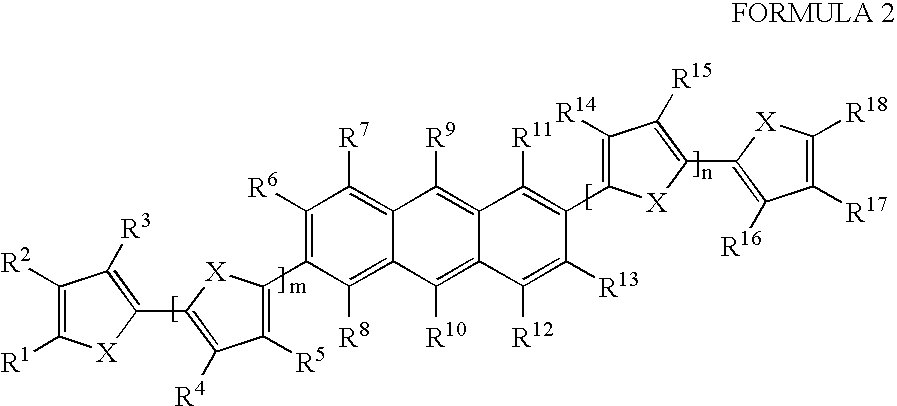

Priority Applications (1)
| Application Number | Priority Date | Filing Date | Title |
|---|---|---|---|
| US12/028,573 US7781761B2 (en) | 2004-11-02 | 2008-02-08 | Substituted anthracenes and electronic devices containing the substituted anthracenes |
Applications Claiming Priority (3)
| Application Number | Priority Date | Filing Date | Title |
|---|---|---|---|
| US62455504P | 2004-11-02 | 2004-11-02 | |
| US11/265,696 US7355199B2 (en) | 2004-11-02 | 2005-11-02 | Substituted anthracenes and electronic devices containing the substituted anthracenes |
| US12/028,573 US7781761B2 (en) | 2004-11-02 | 2008-02-08 | Substituted anthracenes and electronic devices containing the substituted anthracenes |
Related Parent Applications (1)
| Application Number | Title | Priority Date | Filing Date |
|---|---|---|---|
| US11/265,696 Division US7355199B2 (en) | 2004-11-02 | 2005-11-02 | Substituted anthracenes and electronic devices containing the substituted anthracenes |
Publications (2)
| Publication Number | Publication Date |
|---|---|
| US20080210933A1 true US20080210933A1 (en) | 2008-09-04 |
| US7781761B2 US7781761B2 (en) | 2010-08-24 |
Family
ID=36087347
Family Applications (2)
| Application Number | Title | Priority Date | Filing Date |
|---|---|---|---|
| US11/265,696 Expired - Fee Related US7355199B2 (en) | 2004-11-02 | 2005-11-02 | Substituted anthracenes and electronic devices containing the substituted anthracenes |
| US12/028,573 Expired - Fee Related US7781761B2 (en) | 2004-11-02 | 2008-02-08 | Substituted anthracenes and electronic devices containing the substituted anthracenes |
Family Applications Before (1)
| Application Number | Title | Priority Date | Filing Date |
|---|---|---|---|
| US11/265,696 Expired - Fee Related US7355199B2 (en) | 2004-11-02 | 2005-11-02 | Substituted anthracenes and electronic devices containing the substituted anthracenes |
Country Status (2)
| Country | Link |
|---|---|
| US (2) | US7355199B2 (en) |
| WO (1) | WO2006050496A1 (en) |
Cited By (4)
| Publication number | Priority date | Publication date | Assignee | Title |
|---|---|---|---|---|
| US20080299474A1 (en) * | 2007-05-31 | 2008-12-04 | Xerox Corporation | High quality substituted aryl diamine and a photoreceptor |
| US20100173436A1 (en) * | 2009-01-05 | 2010-07-08 | Dalsa Semiconductor Inc. | Method of making biomems devices |
| WO2010138650A1 (en) * | 2009-05-28 | 2010-12-02 | Corning Incorporated | Fused thiophenes, articles, and methods thereof |
| KR101736920B1 (en) | 2009-12-15 | 2017-05-18 | 엘지디스플레이 주식회사 | Aryl-substituted anthracene compound, preparation method thereof, and organic thin film transistor comprising the same |
Families Citing this family (35)
| Publication number | Priority date | Publication date | Assignee | Title |
|---|---|---|---|---|
| DE10353094A1 (en) * | 2003-11-12 | 2005-06-09 | H.C. Starck Gmbh | Process for preparing linear organic thiophene-phenylene oligomers |
| GB2408209A (en) * | 2003-11-18 | 2005-05-25 | Qinetiq Ltd | Flexible medical light source |
| US8927114B2 (en) * | 2004-11-30 | 2015-01-06 | Semiconductor Energy Laboratory Co., Ltd. | Light emitting element and electronic device using the same |
| GB0506899D0 (en) * | 2005-04-05 | 2005-05-11 | Plastic Logic Ltd | Multiple conductive layer TFT |
| US20060231829A1 (en) * | 2005-04-13 | 2006-10-19 | Xerox Corporation | TFT gate dielectric with crosslinked polymer |
| CN101687385A (en) * | 2005-05-12 | 2010-03-31 | 佐治亚科技研究公司 | Metal oxide nanoparticles that coats and preparation method thereof |
| KR100708720B1 (en) * | 2005-10-19 | 2007-04-17 | 삼성에스디아이 주식회사 | A organic thin film transistor, a method for preparing the same and a flat panel display comprising the same |
| US20070102697A1 (en) * | 2005-11-10 | 2007-05-10 | Fang-Chung Chen | Junction structure of organic semiconductor device, organic thin film transistor and fabricating method thereof |
| US7566899B2 (en) * | 2005-12-21 | 2009-07-28 | Palo Alto Research Center Incorporated | Organic thin-film transistor backplane with multi-layer contact structures and data lines |
| US8138075B1 (en) | 2006-02-06 | 2012-03-20 | Eberlein Dietmar C | Systems and methods for the manufacture of flat panel devices |
| US7586120B2 (en) * | 2006-04-06 | 2009-09-08 | Xerox Corporation | Ethynylene acene polymers and electronic devices generated therefrom |
| US7550760B2 (en) * | 2006-04-06 | 2009-06-23 | Xerox Corporation | Polyacenes and electronic devices generated therefrom |
| US7495251B2 (en) * | 2006-04-21 | 2009-02-24 | 3M Innovative Properties Company | Electronic devices containing acene-thiophene copolymers with silylethynyl groups |
| KR101320382B1 (en) * | 2006-05-22 | 2013-10-29 | 삼성디스플레이 주식회사 | Organic light emitting compound and organic light emitting device comprising the same |
| US7528448B2 (en) | 2006-07-17 | 2009-05-05 | E.I. Du Pont De Nemours And Company | Thin film transistor comprising novel conductor and dielectric compositions |
| US8405069B2 (en) * | 2006-11-10 | 2013-03-26 | Georgia Tech Research Corporation | Printable thin-film transistors with high dielectric constant gate insulators and methods for producing same |
| US8026512B2 (en) * | 2006-11-16 | 2011-09-27 | Panasonic Corporation | Mobility engineered electroluminescent devices |
| US7923718B2 (en) * | 2006-11-29 | 2011-04-12 | Xerox Corporation | Organic thin film transistor with dual layer electrodes |
| KR100877177B1 (en) | 2007-03-30 | 2009-01-09 | 경상대학교산학협력단 | Organic semiconductor containing acetylenic anthracene, and Organic thin film transistor using the same |
| KR100901885B1 (en) | 2007-04-11 | 2009-06-09 | 경상대학교산학협력단 | Organic Semiconductor Terminally Functionalized By Naphthalene Having Electron Donating Substituents, And Organic Thin Film Transistor Using The Same |
| WO2008120839A1 (en) * | 2007-03-30 | 2008-10-09 | Gyeongsang National University Industrial And Academic Collaboration Foundation | Novel organic semiconductor compound, and organic thin film transistor using the same |
| WO2009031681A1 (en) * | 2007-09-07 | 2009-03-12 | Nec Corporation | Switching device and method for manufacturing the same |
| JP5333221B2 (en) * | 2007-09-07 | 2013-11-06 | 日本電気株式会社 | Carbon nanotube structure and thin film transistor |
| JP2011508967A (en) | 2007-12-17 | 2011-03-17 | スリーエム イノベイティブ プロパティズ カンパニー | Solution processable organic semiconductors based on anthracene |
| KR100901887B1 (en) * | 2008-03-14 | 2009-06-09 | (주)그라쎌 | Novel organic electroluminescent compounds and organic electroluminescent device using the same |
| WO2009133917A1 (en) * | 2008-04-30 | 2009-11-05 | 出光興産株式会社 | Anthracene derivative and organic electroluminescent element using the same |
| CN102119164A (en) * | 2008-06-19 | 2011-07-06 | 3M创新有限公司 | Solution processable organic semiconductors |
| KR101022494B1 (en) * | 2008-11-28 | 2011-03-16 | 고려대학교 산학협력단 | Carbon Nano Tube Thin film Transistor and display adopting the same |
| WO2010111534A1 (en) * | 2009-03-27 | 2010-09-30 | Presidio Pharmaceuticals, Inc. | Fused ring inhibitors of hepatitis c |
| CA2760205A1 (en) * | 2009-05-12 | 2010-11-18 | Schering Corporation | Fused tricyclic aryl compounds useful for the treatment of viral diseases |
| EP2606530B1 (en) | 2010-08-20 | 2017-04-26 | Rhodia Operations | Polymer compositions, polymer films, polymer gels, polymer foams, and electronic devices containing such films, gels, and foams |
| US9525071B2 (en) * | 2012-02-22 | 2016-12-20 | Massachusetts Institute Of Technology | Flexible high-voltage thin film transistors |
| US9082735B1 (en) * | 2014-08-14 | 2015-07-14 | Srikanth Sundararajan | 3-D silicon on glass based organic light emitting diode display |
| CN113087727A (en) * | 2021-03-31 | 2021-07-09 | 广州追光科技有限公司 | Anthracene-thieno [3,4-b ] thiophene-based compounds and their use in organic electronic devices |
| CN113307819A (en) * | 2021-04-02 | 2021-08-27 | 广州追光科技有限公司 | Anthracene-thieno [3,4-b ] thiophene-based compounds and their use in organic electronic devices |
Citations (5)
| Publication number | Priority date | Publication date | Assignee | Title |
|---|---|---|---|---|
| US6107117A (en) * | 1996-12-20 | 2000-08-22 | Lucent Technologies Inc. | Method of making an organic thin film transistor |
| US6452207B1 (en) * | 2001-03-30 | 2002-09-17 | Lucent Technologies Inc. | Organic semiconductor devices |
| US20030095445A1 (en) * | 2001-11-22 | 2003-05-22 | Mitsubishi Denki Kabushiki Kaisha | Semiconductor memory device |
| US20050005572A1 (en) * | 2003-07-11 | 2005-01-13 | Perkins Darcie Woodruff | Window box and mounting system |
| US20050019198A1 (en) * | 2001-11-28 | 2005-01-27 | Thomas Salomon | Auto suction hybrid pump |
Family Cites Families (4)
| Publication number | Priority date | Publication date | Assignee | Title |
|---|---|---|---|---|
| US6998068B2 (en) * | 2003-08-15 | 2006-02-14 | 3M Innovative Properties Company | Acene-thiophene semiconductors |
| WO2003095445A1 (en) * | 2002-05-07 | 2003-11-20 | Lg Chem, Ltd. | New organic compounds for electroluminescence and organic electroluminescent devices using the same |
| US20040119049A1 (en) * | 2002-12-04 | 2004-06-24 | Martin Heeney | Mono-, oligo- and poly-bis(thienyl) arylenes and their use as charge transport materials |
| EP1644460B1 (en) | 2003-07-10 | 2008-01-30 | MERCK PATENT GmbH | Substituted anthracenes |
-
2005
- 2005-11-02 US US11/265,696 patent/US7355199B2/en not_active Expired - Fee Related
- 2005-11-02 WO PCT/US2005/039947 patent/WO2006050496A1/en active Application Filing
-
2008
- 2008-02-08 US US12/028,573 patent/US7781761B2/en not_active Expired - Fee Related
Patent Citations (5)
| Publication number | Priority date | Publication date | Assignee | Title |
|---|---|---|---|---|
| US6107117A (en) * | 1996-12-20 | 2000-08-22 | Lucent Technologies Inc. | Method of making an organic thin film transistor |
| US6452207B1 (en) * | 2001-03-30 | 2002-09-17 | Lucent Technologies Inc. | Organic semiconductor devices |
| US20030095445A1 (en) * | 2001-11-22 | 2003-05-22 | Mitsubishi Denki Kabushiki Kaisha | Semiconductor memory device |
| US20050019198A1 (en) * | 2001-11-28 | 2005-01-27 | Thomas Salomon | Auto suction hybrid pump |
| US20050005572A1 (en) * | 2003-07-11 | 2005-01-13 | Perkins Darcie Woodruff | Window box and mounting system |
Cited By (7)
| Publication number | Priority date | Publication date | Assignee | Title |
|---|---|---|---|---|
| US20080299474A1 (en) * | 2007-05-31 | 2008-12-04 | Xerox Corporation | High quality substituted aryl diamine and a photoreceptor |
| US20100173436A1 (en) * | 2009-01-05 | 2010-07-08 | Dalsa Semiconductor Inc. | Method of making biomems devices |
| US7927904B2 (en) * | 2009-01-05 | 2011-04-19 | Dalsa Semiconductor Inc. | Method of making BIOMEMS devices |
| WO2010138650A1 (en) * | 2009-05-28 | 2010-12-02 | Corning Incorporated | Fused thiophenes, articles, and methods thereof |
| US20110166307A1 (en) * | 2009-05-28 | 2011-07-07 | Mingqian He | Fused thiophenes, articles, and methods thereof |
| US8278410B2 (en) | 2009-05-28 | 2012-10-02 | Corning Incorporated | Fused thiophenes, articles, and methods thereof |
| KR101736920B1 (en) | 2009-12-15 | 2017-05-18 | 엘지디스플레이 주식회사 | Aryl-substituted anthracene compound, preparation method thereof, and organic thin film transistor comprising the same |
Also Published As
| Publication number | Publication date |
|---|---|
| US20060131570A1 (en) | 2006-06-22 |
| US7781761B2 (en) | 2010-08-24 |
| US7355199B2 (en) | 2008-04-08 |
| WO2006050496A1 (en) | 2006-05-11 |
Similar Documents
| Publication | Publication Date | Title |
|---|---|---|
| US7781761B2 (en) | Substituted anthracenes and electronic devices containing the substituted anthracenes | |
| JP5155852B2 (en) | Aryl-ethylene substituted aromatic compounds and their use as organic semiconductors | |
| JP5622585B2 (en) | Novel heterocyclic compounds and their use | |
| US7385221B1 (en) | Silylethynylated heteroacenes and electronic devices made therewith | |
| TWI508991B (en) | Ambipolar polymeric semiconductor materials and organic electronic devices | |
| KR101096981B1 (en) | New fused ring compound and organic electronic device using the same | |
| TWI588150B (en) | Heterocyclic compound and use thereof | |
| KR101622303B1 (en) | High-Performance Organic Semiconductors Based on 2,7-Bis-(vinyl)[1]benzothieno[3,2-b]benzothiophene Backbone and the Organic Semiconductor Thin-Film using the same and Organic Thin-Film Transistors using thereof | |
| TWI549327B (en) | Organic field effect transistor and organic semiconductor material | |
| US20090036689A1 (en) | Substituted indolocarbazoles | |
| US7655807B2 (en) | Low molecular weight conjugated nitrogen compounds and devices fabricated using the same | |
| WO2012115218A1 (en) | Method for producing dianthra[2,3-b:2',3'-f]thieno[3,2-b]thiophene, and use thereof | |
| JP2015199716A (en) | Polycyclic fused ring compound, organic semiconductor material, organic semiconductor device, and organic transistor | |
| KR100868863B1 (en) | New fused ring compound and organic electronic device using the same | |
| JP2015501298A (en) | Pyrrolo-pyrroledione-thiophenequinone compound, preparation method and use thereof | |
| Duan et al. | Organic field-effect transistors based on two phenylene–thiophene oligomer derivatives with a biphenyl or fluorene core | |
| Um et al. | High-performance organic semiconductors for thin-film transistors based on 2, 7-divinyl [1] benzothieno [3, 2-b] benzothiophene | |
| JP5600267B2 (en) | Novel compounds and their use | |
| US8021578B2 (en) | Fused thiophene acenes and organic semiconductors made therefrom | |
| JP6592863B2 (en) | Organic compounds and their uses | |
| WO2021054161A1 (en) | Fused polycyclic aromatic compound | |
| US7586120B2 (en) | Ethynylene acene polymers and electronic devices generated therefrom | |
| Yang | Development of π-Extended Heteroacene-based Materials toward Application in Organic Field-Effect Transistors |
Legal Events
| Date | Code | Title | Description |
|---|---|---|---|
| AS | Assignment |
Owner name: E. I. DU PONT DE NEMOURS AND COMPANY, DELAWARE Free format text: ASSIGNMENT OF ASSIGNORS INTEREST;ASSIGNOR:MENG, HONG;REEL/FRAME:020798/0044 Effective date: 20080324 |
|
| AS | Assignment |
Owner name: E. I. DU PONT DE NEMOURS AND COMPANY, DELAWARE Free format text: ASSIGNMENT OF ASSIGNORS INTEREST;ASSIGNOR:MENG, HONG;REEL/FRAME:021177/0327 Effective date: 20080324 |
|
| REMI | Maintenance fee reminder mailed | ||
| LAPS | Lapse for failure to pay maintenance fees | ||
| STCH | Information on status: patent discontinuation |
Free format text: PATENT EXPIRED DUE TO NONPAYMENT OF MAINTENANCE FEES UNDER 37 CFR 1.362 |
|
| FP | Lapsed due to failure to pay maintenance fee |
Effective date: 20140824 |