US20070034860A1 - Field effect organic transistor - Google Patents
Field effect organic transistor Download PDFInfo
- Publication number
- US20070034860A1 US20070034860A1 US10/555,303 US55530304A US2007034860A1 US 20070034860 A1 US20070034860 A1 US 20070034860A1 US 55530304 A US55530304 A US 55530304A US 2007034860 A1 US2007034860 A1 US 2007034860A1
- Authority
- US
- United States
- Prior art keywords
- organic
- semiconductive layer
- field effect
- organic semiconductive
- mobility
- Prior art date
- Legal status (The legal status is an assumption and is not a legal conclusion. Google has not performed a legal analysis and makes no representation as to the accuracy of the status listed.)
- Granted
Links
Images


Classifications
-
- H—ELECTRICITY
- H10—SEMICONDUCTOR DEVICES; ELECTRIC SOLID-STATE DEVICES NOT OTHERWISE PROVIDED FOR
- H10K—ORGANIC ELECTRIC SOLID-STATE DEVICES
- H10K10/00—Organic devices specially adapted for rectifying, amplifying, oscillating or switching; Organic capacitors or resistors having a potential-jump barrier or a surface barrier
- H10K10/40—Organic transistors
- H10K10/46—Field-effect transistors, e.g. organic thin-film transistors [OTFT]
- H10K10/462—Insulated gate field-effect transistors [IGFETs]
- H10K10/484—Insulated gate field-effect transistors [IGFETs] characterised by the channel regions
- H10K10/486—Insulated gate field-effect transistors [IGFETs] characterised by the channel regions the channel region comprising two or more active layers, e.g. forming pn heterojunctions
-
- H—ELECTRICITY
- H10—SEMICONDUCTOR DEVICES; ELECTRIC SOLID-STATE DEVICES NOT OTHERWISE PROVIDED FOR
- H10K—ORGANIC ELECTRIC SOLID-STATE DEVICES
- H10K10/00—Organic devices specially adapted for rectifying, amplifying, oscillating or switching; Organic capacitors or resistors having a potential-jump barrier or a surface barrier
- H10K10/20—Organic diodes
- H10K10/26—Diodes comprising organic-organic junctions
-
- H—ELECTRICITY
- H10—SEMICONDUCTOR DEVICES; ELECTRIC SOLID-STATE DEVICES NOT OTHERWISE PROVIDED FOR
- H10K—ORGANIC ELECTRIC SOLID-STATE DEVICES
- H10K10/00—Organic devices specially adapted for rectifying, amplifying, oscillating or switching; Organic capacitors or resistors having a potential-jump barrier or a surface barrier
- H10K10/40—Organic transistors
- H10K10/46—Field-effect transistors, e.g. organic thin-film transistors [OTFT]
- H10K10/462—Insulated gate field-effect transistors [IGFETs]
- H10K10/466—Lateral bottom-gate IGFETs comprising only a single gate
-
- H—ELECTRICITY
- H10—SEMICONDUCTOR DEVICES; ELECTRIC SOLID-STATE DEVICES NOT OTHERWISE PROVIDED FOR
- H10K—ORGANIC ELECTRIC SOLID-STATE DEVICES
- H10K10/00—Organic devices specially adapted for rectifying, amplifying, oscillating or switching; Organic capacitors or resistors having a potential-jump barrier or a surface barrier
- H10K10/40—Organic transistors
- H10K10/46—Field-effect transistors, e.g. organic thin-film transistors [OTFT]
- H10K10/462—Insulated gate field-effect transistors [IGFETs]
- H10K10/468—Insulated gate field-effect transistors [IGFETs] characterised by the gate dielectrics
-
- H—ELECTRICITY
- H10—SEMICONDUCTOR DEVICES; ELECTRIC SOLID-STATE DEVICES NOT OTHERWISE PROVIDED FOR
- H10K—ORGANIC ELECTRIC SOLID-STATE DEVICES
- H10K85/00—Organic materials used in the body or electrodes of devices covered by this subclass
- H10K85/10—Organic polymers or oligomers
- H10K85/111—Organic polymers or oligomers comprising aromatic, heteroaromatic, or aryl chains, e.g. polyaniline, polyphenylene or polyphenylene vinylene
- H10K85/113—Heteroaromatic compounds comprising sulfur or selene, e.g. polythiophene
- H10K85/1135—Polyethylene dioxythiophene [PEDOT]; Derivatives thereof
-
- H—ELECTRICITY
- H10—SEMICONDUCTOR DEVICES; ELECTRIC SOLID-STATE DEVICES NOT OTHERWISE PROVIDED FOR
- H10K—ORGANIC ELECTRIC SOLID-STATE DEVICES
- H10K85/00—Organic materials used in the body or electrodes of devices covered by this subclass
- H10K85/30—Coordination compounds
- H10K85/311—Phthalocyanine
-
- H—ELECTRICITY
- H10—SEMICONDUCTOR DEVICES; ELECTRIC SOLID-STATE DEVICES NOT OTHERWISE PROVIDED FOR
- H10K—ORGANIC ELECTRIC SOLID-STATE DEVICES
- H10K85/00—Organic materials used in the body or electrodes of devices covered by this subclass
- H10K85/60—Organic compounds having low molecular weight
- H10K85/615—Polycyclic condensed aromatic hydrocarbons, e.g. anthracene
Definitions
- the present invention relates to a field effect organic transistor, in particular, a field effect organic transistor, including an organic semiconductive layer, useful in the electronic field including display devices, information tags, and ICs.
- Organic semiconductors are provided with the characteristics inherent to organic materials including lightweightness, flexibility, diversity, and toughness; organic semiconductors can be formed by the low temperature processes around 100° C., and permit the fabrication method based on the liquid phase processes such as printing and spin coating. Accordingly, the fabrication on the plastic substrates and the enlargement of the image planes, both having been impossible with the crystalline silicon semiconductor, can be possible, and thus, more expectations are placed on the application of organic semiconductors to novel devices such as flexible electronic paper and information tags.
- the usual organic semiconductors are as low as 10 ⁇ 5 to 10 ⁇ 2 cm 2 /Vs in mobility, lower in mobility by an order of magnitude or more than the silicon semiconductors, and thus higher in resistance, so that the organic semiconductors face the problems such that large currents can be hardly obtained and the operation frequencies are low.
- the mobility that can be obtained with a field effect organic transistor can be derived from the formula (I) of the drain current in the saturation region.
- Id ⁇ ( W /2 L ) Ci ( Vg ⁇ Vth ) 2 (I)
- Id denotes the drain current (A)
- ⁇ denotes the mobility (cm 2 /Vs)
- W denotes the channel width (cm)
- L denotes the channel length (cm)
- Ci denotes the capacity of the gate insulating layer (F/cm 2 )
- Vg denotes the gate voltage (V)
- the ratio (on/off ratio) of the current flowing between the source and drain electrodes when the transistor is on to the current flowing between the source drain electrodes when the transistor is off be at least 10 4 or more, preferably 10 6 or more.
- the mobility is low as described above, and hence the on current is small; on the other hand, owing to the effect of the impurities contained in the organic semiconductor, the off current is large; so that a sufficiently large on/off ratio has not yet been obtained. This is conspicuous for polymer compounds.
- a technique for improving the bn/off ratio disclosed in Japanese Patent Application Laid-Open No. 10-190001, has made the mobility be 10 ⁇ 3 cm 2 /Vs or more and the conductivity be 10 ⁇ 5 S/cm or less, and thus has made the on/off ratio be of the order of 10 3 ; however, this is not yet sufficient. Thus, it is the actual condition that there is no field effect organic transistor which utilizes an organic semiconductor capable of satisfying the practical characteristics.
- the present invention has been achieved in view of such conventional techniques, and aims at the provision of a field effect organic transistor which overcomes the above described problems, and is large in mobility and high in on/off ratio.
- the field effect organic transistor provided by the present invention is a field effect organic transistor which includes a source electrode, a drain electrode, a gate electrode, a gate insulating layer and an organic semiconductive layer, the field effect organic transistor being characterized in that:
- the organic semiconductive layer includes a first organic semiconductive layer forming a channel region and a second organic semiconductive layer arranged to abut the first organic semiconductive layer;
- the charge mobility ( ⁇ 1 ) in the first semiconductive layer is 10 ⁇ 3 cm 2 /Vs or more;
- the charge mobility ( ⁇ 2 ) in the second semiconductive layer is 10 ⁇ 4 cm 2 /Vs or less;
- the ratio ( ⁇ 1 / ⁇ 2 ) between the two organic semiconductive layers is 10 or more.
- the present invention includes a device in which the thickness of the first semiconductive layer is made to be 5 to 100 nm.
- the present invention includes a device in which the thickness of the second semiconductive layer is made to be 100 to 1,000 nm.
- the thickness of the channel region is made to be 50 nm or less.
- the present invention includes a device in which the organic semiconductive layer is constructed with a conjugated polymer compound permitting utilizing a liquid phase process for the fabrication of the organic semiconductive layer.
- the present invention includes a device in which the weight average molecular weight of the conjugated polymer compound is made to be 5,000 to 500,000.
- the present invention includes a device in which the gate insulating layer is constructed with an organic compound.
- a field effect organic transistor which is large in mobility and high in on/off ratio can be provided in the field of electronics including display devices, information tags and ICs.
- FIG. 1 is a schematic sectional view illustrating an example of a field effect organic transistor of the present invention.
- FIG. 2 is a schematic sectional view illustrating a field effect organic transistor used in an example of the present invention.
- the structure of the field effect organic transistor of the present invention is effective in any of the planar type, staggered type and inversely staggered type; detailed description will be made on the present invention by taking the planar type as an example with reference to FIG. 1 .
- FIG. 1 is a schematic sectional view illustrating an example of a field effect organic transistor of the present invention.
- the field effect organic transistor of the present invention is constructed by arranging a gate electrode 12 on an insulative substrate 11 , a gate insulating layer 13 thereover, additionally a source electrode 15 and a drain electrode 14 thereover, organic semiconductive layers 16 , 17 thereover, and a protective film 18 as the uppermost portion.
- the present invention is characterized in that the mobilities of the organic semiconductive layers 16 , 17 are different from each other.
- preferable is a device in which the organic semiconductive layer 16 to be a channel region 19 for charge transfer is higher in mobility than the organic semiconductive layer 17 not to be a channel region.
- the channel region used in the present invention broadly means, depending on the channel length, the region from the interface with the gate insulating layer 13 up to the 50 nm or less thick portion of the organic semiconductive layer.
- the method for forming the regions different in mobility from each other in the organic semiconductive layer there can be cited a method in which one type of organic semiconductive layer is used and the orientation condition thereof is varied to form regions different from each other in mobility, and a method in which two or more types of organic semiconductors different in mobility from each other are deposited to form regions different in mobility from each other.
- the orientation condition when the organic semiconductive layer is deposited by a vapor phase method as the method for varying the orientation condition, the orientation condition can be attained by varying the evaporation rate and the substrate temperature.
- the orientation condition can be attained by varying the drying temperature and the type of the environmental gas.
- the mobility ⁇ 1 of the organic semiconductive layer 16 to be the channel region falls in the range of 10 ⁇ 3 cm 2 /Vs or more, preferably 10 ⁇ 2 cm 2 /Vs or more.
- the mobility p2 of the organic semiconductive layer 17 not to be the channel region falls in the range of 10 ⁇ 4 cm 2 /Vs or less, preferably 10 ⁇ 5 cm 2 /Vs or less.
- the two mobilities of the organic semiconductive layers 16 , 17 satisfy the relation ⁇ 1 > ⁇ 2 , and the mobility ratio ( ⁇ 1 / ⁇ 2 ) is preferably 10 or more, and further preferably 100 or more.
- the values of the mobilities of the organic semiconductive layers 16 , 17 indicate the value obtained from the above described formula (I) obtained for the field effect organic transistor.
- the thickness of the organic semiconductive layer 16 is 5 to 100 nm and the thickness of the organic semiconductive layer 17 is 100 to 1000 nm.
- Examples of such compounds include:
- conjugated polymer compounds such as polyacetylene derivatives, polythiophene derivatives having thiophene rings, poly(3-alkylthiophene) derivatives, poly(3,4-ethylenedioxythiophene) derivatives, polythienylenevinylene derivatives, polyphenylene derivatives having benzene rings, polyphenylenevinylene derivatives, polypyridine derivatives having nitrogen atoms, polypyrrole derivatives, polyaniline derivatives, and polyquinoline derivatives;
- oligomers represented by dimethyl sexithiophene and quarterthiophene
- acenes represented by perylene, tetracene and pentacene
- smectic liquid crystals represented by phenylnaphthalene derivatives and benzothiazole derivatives
- liquid crystal polymers represented by poly(9,9-dialkylfluorene-bithiophene) copolymer.
- the compounds concerned are not limited to these compounds.
- R 1 , R 2 , R 3 and R 4 each represent H, F or an alkyl group having 1 to 20 carbon atoms or an alkoxy group having 1 to 20 carbon atoms, and n represents a positive integer.
- the organic semiconductive layer used in the present invention may contain appropriate dopants for the purpose of adjusting the electric conductivity thereof.
- the dopants include acceptor type dopants such as I 2 , Br 2 , Cl 2 , BF 3 , PF 5 , H 2 SO 4 , FeCl 3 and TCNQ (tetracyanoquinodimethane); donor type dopants such as Li, K, Na, Eu; and surfactants such as alkylsulfonates and alkylbenzenesuflonates.
- the gate insulating layer of the present invention there can be used inorganic materials such as SiO 2 , SiN x , Al 2 O 3 and Ta 2 O 5 ; organic materials such as polyimide, polyacrylonitrile, polytetrafluoroethylene, polyvinyl alcohol, polyvinylphenol, polyethylene terephthalate and polyvinylidenefluoride; and organic-inorganic hybrid materials. From the viewpoint that a liquid process leading to low cost can be preferably utilized, organic compounds are preferable.
- the insulative substrate there can be used, in addition to inorganic materials such as glass and quartz, photosensitive polymer compounds such as acrylic based, vinyl based, ester based, imide based, urethane based, diazo based and cinnamoyl photosensitive polymer compounds; organic materials such as polyvinylidenefluoride, polyethylene terephtahlate and polyethylene; and organic-inorganic hybrid materials. Additionally, two or more layers of these materials can be deposited to be used, and this deposition is effective for the purpose of enhancing the withstand voltage.
- photosensitive polymer compounds such as acrylic based, vinyl based, ester based, imide based, urethane based, diazo based and cinnamoyl photosensitive polymer compounds
- organic materials such as polyvinylidenefluoride, polyethylene terephtahlate and polyethylene
- organic-inorganic hybrid materials two or more layers of these materials can be deposited to be used, and this deposition
- gate electrode, source electrode and drain electrode are electric conductors; for example, suitable are metal materials such as Al, Cu, Ti, Au, Pt, Ag and Cr, and inorganic materials such as polysilicone, silicide, ITO (indium tin oxide) and SnO 2 ; and there can be used conducting polymers represented by highly doped polypyridine, polyacetylene, polyaniline, polypyrrole and polythiophene; conducting inks in which carbon particles, silver particles or the like are dispersed; and the like.
- suitable are metal materials such as Al, Cu, Ti, Au, Pt, Ag and Cr, and inorganic materials such as polysilicone, silicide, ITO (indium tin oxide) and SnO 2 ; and there can be used conducting polymers represented by highly doped polypyridine, polyacetylene, polyaniline, polypyrrole and polythiophene; conducting inks in which carbon particles, silver particles or the like are dispersed; and the like.
- each of these electrodes is formed of a conducting polymer, or conducting inks in which carbon particles, silver particles or the like are dispersed because the thermal expansions of these electrodes can be easily conformed with the thermal expansion of the substrate.
- these members can be formed with the aid of the electrolytic polymerization method, the casting method, the spin coating method, the soak-coating method, the screen printing method, the micromold method, the microcontact method, the roll coating method, the inkjet method, the LB method and the like.
- the vacuum deposition method, the CVD method, the electron beam deposition method, the resistance heating deposition method, the sputtering method and the like are also effective formation methods.
- these members can be subjected to the patterning into desired shapes with the aid of the photolithograph and etching treatment.
- the soft lithograph and inkjet methods are also effective methods for patterning.
- extractor electrodes from the respective electrodes, protective films and the like can be formed.
- FIG. 2 illustrates the configuration diagram of the field effect organic transistor used in the example of the present invention.
- FIG. 2 there were used a highly n-type doped silicon substrate for a gate electrode 21 , SiO 2 for a gate insulating layer 22 , a chromium/gold deposition for a source electrode 23 and a drain electrode 24 and dimethylsexithiophene shown below for organic semiconductive layers 25 , 26 .
- the steps of fabrication will be described.
- a thermally-oxidized film of SiO 2 (the film thickness: 300 nm) was formed.
- the chromium (5 nm)/gold (100 nm) source and drain electrodes were formed with a channel length of 50 ⁇ m and a channel width of 50 mm.
- the organic semiconductive layer 25 was formed by depositing dimethylsexithiophene under a pressure of 5 ⁇ 10 ⁇ 6 torr, from Plate metal separated by 10 cm from the deposition substrate, at an average sublimation rate of 0.05 nm/s and at a substrate temperature of 25° C., until the film thickness reached 10 nm.
- the drain current was measured for the gate voltage of 0 V to 50 V and the voltage between the source and drain electrodes of 0 V to 50 V, and thus the mobility ⁇ was derived according to formula (I).
- a field effect organic transistor was fabricated in the same manner as that in Example 1 except that the organic semiconductive layers 25 , 26 were formed under the conditions described below.
- the organic semiconductive layers 25 , 26 were formed by depositing dimethylsexithiophene under a pressure of 5 ⁇ 10 ⁇ 6 torr, from Plate metal separated by 10 cm from the deposition substrate, at an average sublimation rate of 1 nm/s and at a substrate temperature of 25° C., until the film thickness reached 300 nm.
- a field effect organic transistor was fabricated in the same manner as that in Example 1 except that the organic semiconductive layers 25 , 26 were formed under the conditions described below.
- the organic semiconductive layers 25 , 26 were formed by depositing dimethylsexithiophene under a pressure of 5 ⁇ 10 ⁇ 6 torr, from Plate metal separated by 10 cm from the deposition substrate, at an average sublimation rate of 0.05 nm/s and at a substrate temperature of 25° C., until the film thickness reached 300 nm.
- FIG. 2 illustrates the configuration diagram of the field effect organic transistor used in the example of the present invention.
- the steps of fabrication will be described.
- a thermally-oxidized film of SiO 2 300 nm was formed.
- the chromium (5 nm)/gold (100 nm) source and drain electrodes were formed with a channel length of 20 ⁇ m and a channel width of 50 mm.
- the organic semiconductive layer 25 was formed by depositing copper phthalocyanine under a pressure of 3 ⁇ 10 ⁇ 6 torr, from Plate metal separated by 10 cm from the deposition substrate, at an average sublimation rate of 0.1 nm/s and at a substrate temperature of 120° C., until the film thickness reached 20 nm.
- a field effect organic transistor was fabricated in the same manner as that in Example 1 except that the organic semiconductive layers 25 , 26 were formed under the conditions described below.
- the organic semiconductive layers 25 , 26 were formed by depositing copper phthalocyanine, from Plate metal, at an average sublimation rate of 1 nm/s and at a substrate temperature of ⁇ 50° C., until the film thickness reached 500 nm.
- a field effect organic transistor was fabricated in the same manner as that in Example 1 except that the organic semiconductive layers 25 , 26 were formed under the conditions described below.
- the organic semiconductive layers 25 , 26 were formed by depositing copper phthalocyanine, from Plate metal, at an average sublimation rate of 0.1 nm/s and at a substrate temperature of 120° C., until the film thickness reached 500 nm.
- FIG. 2 illustrates the configuration diagram of the field effect organic transistor used in the example of the present invention.
- the organic semiconductive layer 25 was formed by depositing pentacene under a pressure of 1 ⁇ 10 ⁇ 6 torr, from Plate metal separated by 10 cm from the deposition substrate, at an average sublimation rate of 0.05 nm/s and at a substrate temperature of 25° C., until the film thickness reached 10 nm.
- the organic semiconductive layer 26 was formed by subliming copper phthalocyanine at an average sublimation rate of 1 nm/s and at a substrate temperature of ⁇ 50° C., until the film thickness reached 300 nm.
- a gold wire of 0.1 mm in diameter was wired to each of the gate electrode, drain electrode and source electrode, with the aid of silver paste, and thus a field effect organic transistor was fabricated.
- the mobility of the organic semiconductive layer 25 made of pentacene is 1.4 ⁇ 10 ⁇ 1 cm 2 /Vs
- the mobility of the organic semiconductive layer 26 made of copper phthalocyanine is 4.6 ⁇ 10 ⁇ 8 cm 2 /Vs.
- FIG. 2 illustrates the configuration diagram of the field effect organic transistor used in the example of the present invention.
- regioirregular poly(3-hexylthiophene) (the weight average molecular weight: 12,000) for the organic semiconductive layer 26 .
- a thermally-oxidized film of SiO 2 300 nm was formed.
- the chromium (5 nm)/gold (100 nm) source and drain electrodes were formed with a channel length of 50 ⁇ m and a channel width of 50 mm.
- a tetrahydrofuran solution of poly (3,4-ethylenedioxythiophene) (0.001 g/ml) was applied with the aid of the spin coating method, dried at 150° C. for 12 hours, and thus the organic semiconductive layer 25 of 50 nm in film thickness was formed.
- a field effect organic transistor was fabricated in the same manner as that in Example 4 except that regioirregular poly (3-hexylthiophene) (the weight average molecular weight:46,000) was used for the organic semiconductive layer 25 .
Abstract
A field effect organic transistor includes a source electrode, a drain electrode, a gate electrode, a gate insulating layer and an organic semiconductive layer; in the field effect organic transistor, the organic semiconductive layer includes a first organic semiconductive layer forming a channel region and a second organic semiconductive layer arranged to abut the first organic semiconductive layer; the charge mobility (mu<SUB>1</SUB>) in the first organic semiconductive layer is 10<SUP>-3 </SUP>cm<SUP>2</SUP>/Vs or more; the charge mobility (mu<SUB>2</SUB>) in the second organic semiconductive layer is 10<SUP>-4 </SUP>cm<SUP>2</SUP>/Vs or less; and the ratio (mu<SUB>1</SUB>/mu<SUB>2</SUB>) between the two organic semiconductive layers is 10 or more.
Description
- 1. Technical Field
- The present invention relates to a field effect organic transistor, in particular, a field effect organic transistor, including an organic semiconductive layer, useful in the electronic field including display devices, information tags, and ICs.
- 2. Background Art
- In rivalry with the silicon transistor based on the crystalline silicon technology, the development of the transistors utilizing organic semiconductors has been actively carried out. Organic semiconductors are provided with the characteristics inherent to organic materials including lightweightness, flexibility, diversity, and toughness; organic semiconductors can be formed by the low temperature processes around 100° C., and permit the fabrication method based on the liquid phase processes such as printing and spin coating. Accordingly, the fabrication on the plastic substrates and the enlargement of the image planes, both having been impossible with the crystalline silicon semiconductor, can be possible, and thus, more expectations are placed on the application of organic semiconductors to novel devices such as flexible electronic paper and information tags.
- However, the usual organic semiconductors are as low as 10−5 to 10−2 cm2/Vs in mobility, lower in mobility by an order of magnitude or more than the silicon semiconductors, and thus higher in resistance, so that the organic semiconductors face the problems such that large currents can be hardly obtained and the operation frequencies are low.
- The mobility that can be obtained with a field effect organic transistor can be derived from the formula (I) of the drain current in the saturation region.
Id=μ(W/2L)Ci(Vg−Vth)2 (I)
In this formula, Id denotes the drain current (A), μ denotes the mobility (cm2/Vs), W denotes the channel width (cm), L denotes the channel length (cm), Ci denotes the capacity of the gate insulating layer (F/cm2), Vg denotes the gate voltage (V), Vth denotes the threshold voltage (V) of the transistor, which can be obtained from the relation between the square root of the drain current and the gate voltage by extrapolation to the drain current Id=0. - Additionally, when used as a switching device, it is necessary that the ratio (on/off ratio) of the current flowing between the source and drain electrodes when the transistor is on to the current flowing between the source drain electrodes when the transistor is off be at least 104 or more, preferably 106 or more. However, in the case of an organic semiconductor, the mobility is low as described above, and hence the on current is small; on the other hand, owing to the effect of the impurities contained in the organic semiconductor, the off current is large; so that a sufficiently large on/off ratio has not yet been obtained. This is conspicuous for polymer compounds.
- A technique for improving the bn/off ratio, disclosed in Japanese Patent Application Laid-Open No. 10-190001, has made the mobility be 10−3 cm2/Vs or more and the conductivity be 10−5 S/cm or less, and thus has made the on/off ratio be of the order of 103; however, this is not yet sufficient. Thus, it is the actual condition that there is no field effect organic transistor which utilizes an organic semiconductor capable of satisfying the practical characteristics.
- The present invention has been achieved in view of such conventional techniques, and aims at the provision of a field effect organic transistor which overcomes the above described problems, and is large in mobility and high in on/off ratio.
- The field effect organic transistor provided by the present invention is a field effect organic transistor which includes a source electrode, a drain electrode, a gate electrode, a gate insulating layer and an organic semiconductive layer, the field effect organic transistor being characterized in that:
- the organic semiconductive layer includes a first organic semiconductive layer forming a channel region and a second organic semiconductive layer arranged to abut the first organic semiconductive layer;
- the charge mobility (μ1) in the first semiconductive layer is 10−3 cm2/Vs or more;
- the charge mobility (μ2) in the second semiconductive layer is 10−4 cm2/Vs or less; and
- the ratio (μ1/μ2) between the two organic semiconductive layers is 10 or more.
- The present invention includes a device in which the thickness of the first semiconductive layer is made to be 5 to 100 nm.
- The present invention includes a device in which the thickness of the second semiconductive layer is made to be 100 to 1,000 nm.
- Additionally, there is included a device in which the thickness of the channel region is made to be 50 nm or less.
- The present invention includes a device in which the organic semiconductive layer is constructed with a conjugated polymer compound permitting utilizing a liquid phase process for the fabrication of the organic semiconductive layer.
- The present invention includes a device in which the weight average molecular weight of the conjugated polymer compound is made to be 5,000 to 500,000.
- Additionally, the present invention includes a device in which the gate insulating layer is constructed with an organic compound.
- According to the present invention, a field effect organic transistor which is large in mobility and high in on/off ratio can be provided in the field of electronics including display devices, information tags and ICs.
-
FIG. 1 is a schematic sectional view illustrating an example of a field effect organic transistor of the present invention; and -
FIG. 2 is a schematic sectional view illustrating a field effect organic transistor used in an example of the present invention. - The structure of the field effect organic transistor of the present invention is effective in any of the planar type, staggered type and inversely staggered type; detailed description will be made on the present invention by taking the planar type as an example with reference to
FIG. 1 . -
FIG. 1 is a schematic sectional view illustrating an example of a field effect organic transistor of the present invention. In this figure, the field effect organic transistor of the present invention is constructed by arranging agate electrode 12 on aninsulative substrate 11, agate insulating layer 13 thereover, additionally asource electrode 15 and adrain electrode 14 thereover, organicsemiconductive layers protective film 18 as the uppermost portion. - The present invention is characterized in that the mobilities of the organic
semiconductive layers semiconductive layer 16 to be achannel region 19 for charge transfer is higher in mobility than the organicsemiconductive layer 17 not to be a channel region. The channel region used in the present invention broadly means, depending on the channel length, the region from the interface with thegate insulating layer 13 up to the 50 nm or less thick portion of the organic semiconductive layer. - As the method for forming the regions different in mobility from each other in the organic semiconductive layer, there can be cited a method in which one type of organic semiconductive layer is used and the orientation condition thereof is varied to form regions different from each other in mobility, and a method in which two or more types of organic semiconductors different in mobility from each other are deposited to form regions different in mobility from each other. In the case of the former, as the method for varying the orientation condition, when the organic semiconductive layer is deposited by a vapor phase method as the method for varying the orientation condition, the orientation condition can be attained by varying the evaporation rate and the substrate temperature. When deposited by a liquid phase method, the orientation condition can be attained by varying the drying temperature and the type of the environmental gas.
- Additionally, in order to make the effect of the present invention effective, the mobility μ1 of the organic
semiconductive layer 16 to be the channel region falls in the range of 10−3 cm2/Vs or more, preferably 10−2 cm2/Vs or more. - Additionally, the mobility p2 of the organic
semiconductive layer 17 not to be the channel region falls in the range of 10−4 cm2/Vs or less, preferably 10−5 cm2/Vs or less. - Additionally, in order to make the effect of the present invention effective, the two mobilities of the organic
semiconductive layers - The values of the mobilities of the organic
semiconductive layers - Additionally, it is preferable that the thickness of the organic
semiconductive layer 16 is 5 to 100 nm and the thickness of the organicsemiconductive layer 17 is 100 to 1000 nm. - No particular constraint is imposed on the organic semiconductive layer used in the present invention, as far as the layer is formed of a conjugated compound having conjugated double bonds. For example, the compounds listed below are preferable.
- Examples of such compounds include:
- conjugated polymer compounds such as polyacetylene derivatives, polythiophene derivatives having thiophene rings, poly(3-alkylthiophene) derivatives, poly(3,4-ethylenedioxythiophene) derivatives, polythienylenevinylene derivatives, polyphenylene derivatives having benzene rings, polyphenylenevinylene derivatives, polypyridine derivatives having nitrogen atoms, polypyrrole derivatives, polyaniline derivatives, and polyquinoline derivatives;
- oligomers represented by dimethyl sexithiophene and quarterthiophene;
- acenes represented by perylene, tetracene and pentacene;
- deposited organic molecules represented by copper phthalocyanine derivatives;
- discotic liquid crystals represented by triphenylene derivatives;
- smectic liquid crystals represented by phenylnaphthalene derivatives and benzothiazole derivatives; and
- liquid crystal polymers represented by poly(9,9-dialkylfluorene-bithiophene) copolymer. However, the compounds concerned are not limited to these compounds.
- Additionally, from the viewpoint that a liquid phase process can be preferably utilized, the above described polymer compounds having conjugated structure are suitable. For example, there can be cited the following compounds having the structures shown below.

In the above formulas, R1, R2, R3 and R4 each represent H, F or an alkyl group having 1 to 20 carbon atoms or an alkoxy group having 1 to 20 carbon atoms, and n represents a positive integer. - No particular constraint is imposed on the weight average molecular weights of these conjugated polymer compounds, but in consideration of the solubility in solvents and the film formability, it is desirable that the molecular weights concerned are 5,000 to 500,000, and preferably 10,000 to 100,000.
- Additionally, the organic semiconductive layer used in the present invention may contain appropriate dopants for the purpose of adjusting the electric conductivity thereof. Examples of the dopants include acceptor type dopants such as I2, Br2, Cl2, BF3, PF5, H2SO4, FeCl3 and TCNQ (tetracyanoquinodimethane); donor type dopants such as Li, K, Na, Eu; and surfactants such as alkylsulfonates and alkylbenzenesuflonates.
- No particular constraint is imposed on the gate insulating layer of the present invention; there can be used inorganic materials such as SiO2, SiNx, Al2O3 and Ta2O5; organic materials such as polyimide, polyacrylonitrile, polytetrafluoroethylene, polyvinyl alcohol, polyvinylphenol, polyethylene terephthalate and polyvinylidenefluoride; and organic-inorganic hybrid materials. From the viewpoint that a liquid process leading to low cost can be preferably utilized, organic compounds are preferable.
- No particular constraint is imposed on the insulative substrate; there can be used, in addition to inorganic materials such as glass and quartz, photosensitive polymer compounds such as acrylic based, vinyl based, ester based, imide based, urethane based, diazo based and cinnamoyl photosensitive polymer compounds; organic materials such as polyvinylidenefluoride, polyethylene terephtahlate and polyethylene; and organic-inorganic hybrid materials. Additionally, two or more layers of these materials can be deposited to be used, and this deposition is effective for the purpose of enhancing the withstand voltage.
- Additionally, no particular constraints are imposed on the gate electrode, source electrode and drain electrode as far as these electrodes are electric conductors; for example, suitable are metal materials such as Al, Cu, Ti, Au, Pt, Ag and Cr, and inorganic materials such as polysilicone, silicide, ITO (indium tin oxide) and SnO2; and there can be used conducting polymers represented by highly doped polypyridine, polyacetylene, polyaniline, polypyrrole and polythiophene; conducting inks in which carbon particles, silver particles or the like are dispersed; and the like. In particular, when used in flexible electronic paper and the like, it is preferable that each of these electrodes is formed of a conducting polymer, or conducting inks in which carbon particles, silver particles or the like are dispersed because the thermal expansions of these electrodes can be easily conformed with the thermal expansion of the substrate.
- No particular constraints are imposed on the methods for forming these various electrodes, the gate insulating layer and the organic semiconductive layer; for the cases of organic materials, these members can be formed with the aid of the electrolytic polymerization method, the casting method, the spin coating method, the soak-coating method, the screen printing method, the micromold method, the microcontact method, the roll coating method, the inkjet method, the LB method and the like. Additionally, depending on the materials used, the vacuum deposition method, the CVD method, the electron beam deposition method, the resistance heating deposition method, the sputtering method and the like are also effective formation methods. Additionally, these members can be subjected to the patterning into desired shapes with the aid of the photolithograph and etching treatment. Alternatively, the soft lithograph and inkjet methods are also effective methods for patterning. Additionally, according to need, extractor electrodes from the respective electrodes, protective films and the like can be formed.
- More detailed description will be made below on the present invention on the basis of the examples, but the present invention is not limited by these examples.
-
FIG. 2 illustrates the configuration diagram of the field effect organic transistor used in the example of the present invention. - In
FIG. 2 , there were used a highly n-type doped silicon substrate for agate electrode 21, SiO2 for agate insulating layer 22, a chromium/gold deposition for asource electrode 23 and adrain electrode 24 and dimethylsexithiophene shown below for organicsemiconductive layers 
- Additionally, the synthesis of dimethylsexithiophene followed the synthesis method described in Advanced Materials, 5, 896 (1993), and the compound thus synthesized was used.
- Now, in what follows, the steps of fabrication will be described. On the silicon substrate, a thermally-oxidized film of SiO2 (the film thickness: 300 nm) was formed. Thereover, with the aid of the lift-off method, the chromium (5 nm)/gold (100 nm) source and drain electrodes were formed with a channel length of 50 μm and a channel width of 50 mm. Thereover, the
organic semiconductive layer 25 was formed by depositing dimethylsexithiophene under a pressure of 5×10⁻⁶ torr, from Plate metal separated by 10 cm from the deposition substrate, at an average sublimation rate of 0.05 nm/s and at a substrate temperature of 25° C., until the film thickness reached 10 nm. - Thereafter, with an average sublimation rate of 1 nm/s and at a substrate temperature of 25° C., the deposition was continued until the film thickness reached 300 nm, and thus the
organic semiconductive layer 26 was formed. A gold wire of 0.1 mm in diameter was wired to each of the gate electrode, drain electrode and source electrode, with the aid of silver paste, and thus a field effect organic transistor was fabricated. - In the next place, the drain current was measured for the gate voltage of 0 V to 50 V and the voltage between the source and drain electrodes of 0 V to 50 V, and thus the mobility μ was derived according to formula (I).
- Additionally, the on/off ratio was derived from the ratio between the drain current for the gate voltage Vg=30 V and the drain current for Vg=0 V when a voltage of 30 V was applied as the voltage between the source and drain electrodes. The results obtained are shown below.
Mobility μ=2.1×10⁻² cm2/Vs
On/off ratio=107 - In the next place, the mobilities of the respective organic
semiconductive layers - A field effect organic transistor was fabricated in the same manner as that in Example 1 except that the organic
semiconductive layers - The organic
semiconductive layers - Then, evaluation was carried out in the same manner as that in Example 1, and thus the mobility and on/off ratio were derived. The results obtained are shown below.
Mobility μ=8.1×10⁻⁶ cm2/Vs
On/off ratio=103 - A field effect organic transistor was fabricated in the same manner as that in Example 1 except that the organic
semiconductive layers - The organic
semiconductive layers - Then, evaluation was carried out in the same manner as that in Example 1, and thus the mobility and on/off ratio were derived. The results obtained are shown below.
Mobility μ=2.5×10⁻² cm2/Vs
On/off ratio=105 -
FIG. 2 illustrates the configuration diagram of the field effect organic transistor used in the example of the present invention. - There were used a highly n-type doped silicon substrate for the
gate electrode 21, SiO2 for thegate insulating layer 22, a chromium/gold deposition for thesource electrode 23 and thedrain electrode 24 and copper phthalocyanine shown below for the organicsemiconductive layers 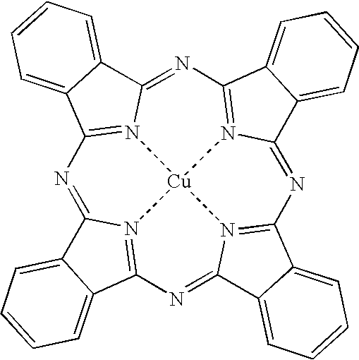
- Now, in what follows, the steps of fabrication will be described. On the silicon substrate, a thermally-oxidized film of SiO2 (300 nm) was formed. Thereover, with the aid of the lift-off method, the chromium (5 nm)/gold (100 nm) source and drain electrodes were formed with a channel length of 20 μm and a channel width of 50 mm. Thereover, the
organic semiconductive layer 25 was formed by depositing copper phthalocyanine under a pressure of 3×10⁻⁶ torr, from Plate metal separated by 10 cm from the deposition substrate, at an average sublimation rate of 0.1 nm/s and at a substrate temperature of 120° C., until the film thickness reached 20 nm. - Thereafter, with an average sublimation rate of 1 nm/s and at a substrate temperature cooled down to −50° C., the deposition was continued until the film thickness reached 500 nm, and thus the
organic semiconductive layer 26 was formed. A gold wire of 0.1 mm in diameter was wired to each of the gate electrode, drain electrode and source electrode, with the aid of silver paste, and thus a field effect organic transistor was fabricated. - Then, evaluation was carried out in the same manner as that in Example 1, and thus the mobility and on/off ratio were derived. The results obtained are shown below.
Mobility μ=9.1×10⁻³ cm2/Vs
On/off ratio=106 - Then, the results are shown below obtained by measuring the mobility of each of the organic
semiconductive layers - A field effect organic transistor was fabricated in the same manner as that in Example 1 except that the organic
semiconductive layers - The organic
semiconductive layers - Then, evaluation was carried out in the same manner as that in Example 1, and thus the mobility and on/off ratio were derived. The results obtained are shown below.
Mobility μ=4.6×10⁻⁸ cm2/Vs
On/off ratio=102 - A field effect organic transistor was fabricated in the same manner as that in Example 1 except that the organic
semiconductive layers - The organic
semiconductive layers - Then, evaluation was carried out in the same manner as that in Example 1, and thus the mobility and on/off ratio were derived. The results obtained are shown below.
Mobility μ=9.3×10⁻³ cm2/Vs
On/off ratio=104 -
FIG. 2 illustrates the configuration diagram of the field effect organic transistor used in the example of the present invention. - There were used a highly n-type doped silicon substrate for the
gate electrode 21, polyacrylonitrile (the weight average molecular weight: 150,000) for thegate insulating layer 22, gold for thesource electrode 23 and thedrain electrode 24, pentacene for theorganic semiconductive layer 25, and copper phthalocyanine for theorganic semiconductive layer 26. - Now, in what follows, the steps of fabrication will be described. On the silicon substrate, a dimethyl sulfoxide solution of polyacrylonitrile (0.1 g/ml) was applied by the spin coating method, and dried at 70° C. for 6 hours and thus the gate insulating layer was formed. Thereover, gold (50 nm) was vacuum deposited, and thus the source and drain electrodes with a channel length of 50 μm and a channel width of 10 mm were fabricated. Thereover, the
organic semiconductive layer 25 was formed by depositing pentacene under a pressure of 1×10⁻⁶ torr, from Plate metal separated by 10 cm from the deposition substrate, at an average sublimation rate of 0.05 nm/s and at a substrate temperature of 25° C., until the film thickness reached 10 nm. - Thereover, the
organic semiconductive layer 26 was formed by subliming copper phthalocyanine at an average sublimation rate of 1 nm/s and at a substrate temperature of −50° C., until the film thickness reached 300 nm. A gold wire of 0.1 mm in diameter was wired to each of the gate electrode, drain electrode and source electrode, with the aid of silver paste, and thus a field effect organic transistor was fabricated. - Then, evaluation was carried out in the same manner as that in Example 1, and thus the mobility and on/off ratio were derived. The results obtained are shown below.
Mobility μ=8.4×10⁻¹ cm2/Vs
On/off ratio=108 - Incidentally, the mobility of the
organic semiconductive layer 25 made of pentacene is 1.4×10⁻¹ cm2/Vs, and the mobility of theorganic semiconductive layer 26 made of copper phthalocyanine is 4.6×10⁻⁸ cm2/Vs. -
FIG. 2 illustrates the configuration diagram of the field effect organic transistor used in the example of the present invention. - There were used a highly n-type doped silicon substrate for the
gate electrode 21, SiO2 for thegate insulating layer 22, a chromium/gold deposition for thesource electrode 23 and thedrain electrode 24 and poly(3,4-ethylenedioxythiophene) (the weight average molecular weight: 10,000) shown below for theorganic semiconductive layer 25.
- There was used regioirregular poly(3-hexylthiophene) (the weight average molecular weight: 12,000) for the
organic semiconductive layer 26. - Now, in what follows, the steps of fabrication will be described. On the
silicon substrate 21, a thermally-oxidized film of SiO2 (300 nm) was formed. Thereover, with the aid of the lift-off method, the chromium (5 nm)/gold (100 nm) source and drain electrodes were formed with a channel length of 50 μm and a channel width of 50 mm. Thereover, a tetrahydrofuran solution of poly (3,4-ethylenedioxythiophene) (0.001 g/ml) was applied with the aid of the spin coating method, dried at 150° C. for 12 hours, and thus theorganic semiconductive layer 25 of 50 nm in film thickness was formed. - Thereover, a chloroform solution of regioirregular poly (3-hexylthiophene) (0.01 g/ml) was applied with the aid of the spin coating method, dried at 120° C. for 6 hours, and thus the
organic semiconductive layer 26 of 500 nm in film thickness was formed. A gold wire of 0.1 mm in diameter was wired to each of the gate electrode, drain electrode and source electrode, with the aid of silver paste, and thus a field effect organic transistor was fabricated. - Then, evaluation was carried out in the same manner as that in Example 1, and thus the mobility and on/off ratio were derived. The results obtained are shown below.
Mobility μ=1.1×10⁻¹ cm2/Vs
On/off ratio=10 6 - A field effect organic transistor was fabricated in the same manner as that in Example 4 except that regioirregular poly (3-hexylthiophene) (the weight average molecular weight:46,000) was used for the
organic semiconductive layer 25. - Then, evaluation was carried out in the same manner as that in Example 1, and thus the mobility and on/off ratio were derived. The results obtained are shown below.
Mobility μ=4.2×10⁻³ cm2/Vs
On/off ratio=105
Claims (7)
1. A field effect organic transistor comprising a source electrode, a drain electrode, a gate electrode, a gate insulating layer and an organic semiconductive layer, the field effect organic transistor being characterized in that:
said organic semiconductive layer comprises a first organic semiconductive layer forming a channel region and a second organic semiconductive layer arranged to abut said first organic semiconductive layer;
the charge mobility (μ1) in said first organic semiconductive layer is 10−3 cm2/Vs or more;
the charge mobility (μ2) in said second organic semiconductive layer is 10−4 cm2/Vs or less; and
the ratio (μ1/μ2) between the two organic semiconductive layers is 10 or more.
2. The field effect organic transistor according to claim 1 , wherein the thickness of said first organic semiconductive layer is made to be 5 nm to 100 nm.
3. The field effect organic transistor according to claim 1 , wherein the thickness of said second organic semiconductive layer is made to be 100 nm to 1000 nm.
4. The field effect organic transistor according to claim 1 , wherein the thickness of said channel region is made to be 50 nm or less.
5. The field effect organic transistor according to claim 1 , wherein said organic semiconductive layer is constructed with a conjugated polymer compound.
6. The field effect organic transistor according to claim 5 , wherein the weight average molecular weight of said conjugated polymer compound is 5,000 to 500,000.
7. The field effect organic transistor according to claim 1 , wherein said gate insulating layer is constructed with an organic compound.
Applications Claiming Priority (3)
| Application Number | Priority Date | Filing Date | Title |
|---|---|---|---|
| JP2003-196336 | 2003-07-14 | ||
| JP2003196336A JP4194436B2 (en) | 2003-07-14 | 2003-07-14 | Field effect organic transistor |
| PCT/JP2004/009789 WO2005006461A1 (en) | 2003-07-14 | 2004-07-02 | Field effect organic transistor |
Publications (2)
| Publication Number | Publication Date |
|---|---|
| US20070034860A1 true US20070034860A1 (en) | 2007-02-15 |
| US7795611B2 US7795611B2 (en) | 2010-09-14 |
Family
ID=34055790
Family Applications (1)
| Application Number | Title | Priority Date | Filing Date |
|---|---|---|---|
| US10/555,303 Expired - Fee Related US7795611B2 (en) | 2003-07-14 | 2004-07-02 | Field effect organic transistor |
Country Status (3)
| Country | Link |
|---|---|
| US (1) | US7795611B2 (en) |
| JP (1) | JP4194436B2 (en) |
| WO (1) | WO2005006461A1 (en) |
Cited By (20)
| Publication number | Priority date | Publication date | Assignee | Title |
|---|---|---|---|---|
| US20060192199A1 (en) * | 2005-02-25 | 2006-08-31 | Xerox Corporation | Celluloses and devices thereof |
| US20060202196A1 (en) * | 2005-01-20 | 2006-09-14 | Fuji Electric Holdings Co., Ltd. | Transistor |
| US20060234335A1 (en) * | 2004-01-27 | 2006-10-19 | Canon Kabushiki Kaisha | Conjugated thiophene compound, conprising perfluorinated and alkylated sidechains, conductive organic thin film containing the compound, and field-effect type organic transistor employing the thin film |
| US20080035915A1 (en) * | 2005-09-20 | 2008-02-14 | Seiko Epson Corporation | Semiconductor film comprising discrete domains of an organic semiconductor and a method of its fabrication |
| US20080128684A1 (en) * | 2006-12-01 | 2008-06-05 | Samsung Electronics Co., Ltd. | Method for fabricating an organic thin film transistor by oxidation and selective reduction of organic semiconductor material |
| US20090009071A1 (en) * | 2005-12-21 | 2009-01-08 | Sven Murano | Organic Component |
| US20090045728A1 (en) * | 2005-12-23 | 2009-02-19 | Sven Murano | Electronic device with a layer structure of organic layers |
| US20090114907A1 (en) * | 2003-09-19 | 2009-05-07 | Canon Kabushiki Kaisha | Field effect type organic transistor and process for production thereof |
| US20090230844A1 (en) * | 2005-03-15 | 2009-09-17 | Novaled Ag | Light-emitting component |
| DE102008036063A1 (en) | 2008-08-04 | 2010-02-11 | Novaled Ag | Organic field effect transistor |
| US20100065825A1 (en) * | 2006-04-19 | 2010-03-18 | Novaled Ag | Light-Emitting Component |
| DE102008036062A1 (en) | 2008-08-04 | 2010-04-22 | Novaled Ag | Organic field effect transistor |
| US20100135073A1 (en) * | 2007-04-17 | 2010-06-03 | Novaled Ag | Organic electronic memory component, memory component arrangement and method for operating an organic electronic memory component |
| US7911129B2 (en) | 2005-04-13 | 2011-03-22 | Novaled Ag | Arrangement for an organic pin-type light-emitting diode and method for manufacturing |
| US20120032174A1 (en) * | 2010-08-06 | 2012-02-09 | Sony Corporation | Semiconductor device, display device and electronic device |
| US8154014B2 (en) | 2007-08-30 | 2012-04-10 | Idemitsu Kosan, Co., Ltd. | Organic thin film transistor and organic thin film light-emitting transistor |
| WO2012175535A1 (en) | 2011-06-22 | 2012-12-27 | Novaled Ag | Organic electronic component |
| US20130099215A1 (en) * | 2010-05-12 | 2013-04-25 | Teijin Limited | Organic semiconductor film, production method thereof, and contact printing stamp |
| US8502200B2 (en) | 2006-01-11 | 2013-08-06 | Novaled Ag | Electroluminescent light-emitting device comprising an arrangement of organic layers, and method for its production |
| US8653537B2 (en) | 2004-08-13 | 2014-02-18 | Novaled Ag | Layer assembly for a light-emitting component |
Families Citing this family (9)
| Publication number | Priority date | Publication date | Assignee | Title |
|---|---|---|---|---|
| KR100719546B1 (en) | 2005-03-19 | 2007-05-17 | 삼성에스디아이 주식회사 | Organic thin film transistor, flat panel display apparatus comprising the same, and method of manufacturing the organic thin film transistor |
| JP4883558B2 (en) * | 2005-03-25 | 2012-02-22 | 国立大学法人大阪大学 | Bipolar organic field-effect thin-film transistor and method for manufacturing the same |
| CN100578744C (en) * | 2005-06-24 | 2010-01-06 | 柯尼卡美能达控股株式会社 | Organic semiconductor film forming method, organic semiconductor film and organic thin film transistor |
| DE102006019483A1 (en) * | 2006-04-26 | 2007-10-31 | Siemens Ag | Organo-magneto-resistive sensor arrangement for e.g. position measurement, has electronic thin layer component, where arrangement is formed in such a manner that field generating device causes magneto-resistive change in layer component |
| JP5196215B2 (en) * | 2006-09-29 | 2013-05-15 | ソニー株式会社 | Semiconductor device |
| JP5352599B2 (en) * | 2011-01-17 | 2013-11-27 | 株式会社半導体エネルギー研究所 | Semiconductor device |
| EP3108975A1 (en) | 2011-03-24 | 2016-12-28 | Cornell University | Aromatic-cationic peptides and uses of same |
| JP6346092B2 (en) | 2011-10-17 | 2018-06-20 | コーネル ユニヴァーシティー | Aromatic cationic peptides and uses thereof |
| US20220045274A1 (en) * | 2020-08-06 | 2022-02-10 | Facebook Technologies Llc | Ofets having organic semiconductor layer with high carrier mobility and in situ isolation |
Citations (33)
| Publication number | Priority date | Publication date | Assignee | Title |
|---|---|---|---|---|
| US4721601A (en) * | 1984-11-23 | 1988-01-26 | Massachusetts Institute Of Technology | Molecule-based microelectronic devices |
| US5008041A (en) * | 1990-01-30 | 1991-04-16 | Lockheed Corporation | Preparation of conductive polyaniline having controlled molecular weight |
| US5107308A (en) * | 1986-07-04 | 1992-04-21 | Mitsubishi Denki Kabushiki Kaisha | Field-effect transistor |
| US5500537A (en) * | 1989-08-17 | 1996-03-19 | Mitsubishi Denki Kabushiki Kaisha | Field-effect transistor with at least two different semiconductive organic channel compounds |
| US5596208A (en) * | 1994-12-09 | 1997-01-21 | Lucent Technologies Inc. | Article comprising an organic thin film transistor |
| US6107117A (en) * | 1996-12-20 | 2000-08-22 | Lucent Technologies Inc. | Method of making an organic thin film transistor |
| US6278127B1 (en) * | 1994-12-09 | 2001-08-21 | Agere Systems Guardian Corp. | Article comprising an organic thin film transistor adapted for biasing to form a N-type or a P-type transistor |
| US20020164835A1 (en) * | 2001-05-04 | 2002-11-07 | Dimitrakopoulos Christos Dimitrios | Organic n-channel semiconductor device of N,N' 3,4,9,10 perylene tetracarboxylic diimide |
| US20030015698A1 (en) * | 2000-10-03 | 2003-01-23 | Marc Baldo | Organic triodes with novel grid structures and method of production |
| US20030085398A1 (en) * | 2001-11-06 | 2003-05-08 | Seiko Epson Corporation | Organic semiconductor device |
| US6586791B1 (en) * | 2000-07-19 | 2003-07-01 | 3M Innovative Properties Company | Transistor insulator layer incorporating superfine ceramic particles |
| US20030218166A1 (en) * | 2002-05-21 | 2003-11-27 | Semiconductor Energy Laboratory Co., Ltd. | Organic field effect transistor |
| US20040004215A1 (en) * | 2002-05-31 | 2004-01-08 | Hiroyuki Iechi | Vertical organic transistor |
| US6692658B2 (en) * | 1999-12-17 | 2004-02-17 | Canon Kabushiki Kaisha | Electrolyte and secondary cell |
| US20040061104A1 (en) * | 2002-09-27 | 2004-04-01 | Zhenan Bao | Devices with organic crystallite active channels |
| US6720572B1 (en) * | 1999-06-25 | 2004-04-13 | The Penn State Research Foundation | Organic light emitters with improved carrier injection |
| US6737303B2 (en) * | 2002-08-28 | 2004-05-18 | Industrial Technology Research Institute | Process for forming organic semiconducting layer having molecular alignment |
| US20040108562A1 (en) * | 2002-09-11 | 2004-06-10 | Pioneer Corporation | Organic semiconductor device |
| US20040150050A1 (en) * | 2003-01-30 | 2004-08-05 | Changchun Institute Of Applied Chemistry Chinese Academy Of Science | Heterojunction organic semiconductor field effect transistor (FET) with a gate insulation layer and manufacturing process thereof |
| US20040155239A1 (en) * | 2002-08-28 | 2004-08-12 | Changchun Institute Of Applied Chemistry Chinese Academy Of Science | Field effect transistor in sandwich configuration having organic semiconductors and manufacturing process thereof |
| US20040161873A1 (en) * | 2002-11-25 | 2004-08-19 | Dimitrakopoulos Christos D. | Organic underlayers that improve the performance of organic semiconductors |
| US20040178428A1 (en) * | 2003-03-11 | 2004-09-16 | Industrial Technology Research Institute | Organic device including semiconducting layer aligned according to microgrooves of photoresist layer |
| US20040186265A1 (en) * | 2003-03-19 | 2004-09-23 | Xerox Corporation | Polythiophenes and devices thereof |
| US20040195563A1 (en) * | 2003-04-02 | 2004-10-07 | Lucent Technologies Inc. | Electrical detection of selected species |
| US6828582B1 (en) * | 2003-09-04 | 2004-12-07 | Hitachi Ltd. | Thin film transistor, display device and their production |
| US20050064623A1 (en) * | 2003-09-24 | 2005-03-24 | Zhenan Bao | Semiconductor layers with roughness patterning |
| US20050062066A1 (en) * | 2003-09-24 | 2005-03-24 | Lucent Technologies, Inc. | Semiconductor devices having regions of induced high and low conductivity, and methods of making the same |
| US6875996B2 (en) * | 2003-05-20 | 2005-04-05 | Canon Kabushiki Kaisha | Field-effect organic transistor |
| US6936186B2 (en) * | 2000-07-24 | 2005-08-30 | Canon Kabushiki Kaisha | Mesomorphic compound, polymeric mesomorphic compound, and electrolyte and secondary battery including same |
| US20060234151A1 (en) * | 2003-06-11 | 2006-10-19 | Masatoshi Nakagawa | Functional organic thin film, organic thin-film transistor, and methods for producing these |
| US20060234335A1 (en) * | 2004-01-27 | 2006-10-19 | Canon Kabushiki Kaisha | Conjugated thiophene compound, conprising perfluorinated and alkylated sidechains, conductive organic thin film containing the compound, and field-effect type organic transistor employing the thin film |
| US7253848B2 (en) * | 2003-01-30 | 2007-08-07 | Industrial Technology Research Institute | Organic thin film transistor array substrate and liquid crystal display including the same |
| US7470574B2 (en) * | 2004-06-24 | 2008-12-30 | Alcatel-Lucent Usa Inc. | OFET structures with both n- and p-type channels |
Family Cites Families (5)
| Publication number | Priority date | Publication date | Assignee | Title |
|---|---|---|---|---|
| JPH0650778B2 (en) | 1985-08-20 | 1994-06-29 | 松下電器産業株式会社 | Thin film transistor and manufacturing method thereof |
| JPH0638491B2 (en) | 1986-07-04 | 1994-05-18 | 三菱電機株式会社 | Field effect transistor |
| JP3352191B2 (en) | 1993-12-08 | 2002-12-03 | キヤノン株式会社 | Method for manufacturing thin film transistor |
| JP2004165427A (en) | 2002-11-13 | 2004-06-10 | Konica Minolta Holdings Inc | Organic thin film transistor element |
| JP2004260121A (en) | 2003-02-28 | 2004-09-16 | Hitachi Ltd | Organic semiconductor element and method for manufacturing the same, and display unit using the same |
-
2003
- 2003-07-14 JP JP2003196336A patent/JP4194436B2/en not_active Expired - Fee Related
-
2004
- 2004-07-02 WO PCT/JP2004/009789 patent/WO2005006461A1/en active Application Filing
- 2004-07-02 US US10/555,303 patent/US7795611B2/en not_active Expired - Fee Related
Patent Citations (33)
| Publication number | Priority date | Publication date | Assignee | Title |
|---|---|---|---|---|
| US4721601A (en) * | 1984-11-23 | 1988-01-26 | Massachusetts Institute Of Technology | Molecule-based microelectronic devices |
| US5107308A (en) * | 1986-07-04 | 1992-04-21 | Mitsubishi Denki Kabushiki Kaisha | Field-effect transistor |
| US5500537A (en) * | 1989-08-17 | 1996-03-19 | Mitsubishi Denki Kabushiki Kaisha | Field-effect transistor with at least two different semiconductive organic channel compounds |
| US5008041A (en) * | 1990-01-30 | 1991-04-16 | Lockheed Corporation | Preparation of conductive polyaniline having controlled molecular weight |
| US5596208A (en) * | 1994-12-09 | 1997-01-21 | Lucent Technologies Inc. | Article comprising an organic thin film transistor |
| US6278127B1 (en) * | 1994-12-09 | 2001-08-21 | Agere Systems Guardian Corp. | Article comprising an organic thin film transistor adapted for biasing to form a N-type or a P-type transistor |
| US6107117A (en) * | 1996-12-20 | 2000-08-22 | Lucent Technologies Inc. | Method of making an organic thin film transistor |
| US6720572B1 (en) * | 1999-06-25 | 2004-04-13 | The Penn State Research Foundation | Organic light emitters with improved carrier injection |
| US6692658B2 (en) * | 1999-12-17 | 2004-02-17 | Canon Kabushiki Kaisha | Electrolyte and secondary cell |
| US6586791B1 (en) * | 2000-07-19 | 2003-07-01 | 3M Innovative Properties Company | Transistor insulator layer incorporating superfine ceramic particles |
| US6936186B2 (en) * | 2000-07-24 | 2005-08-30 | Canon Kabushiki Kaisha | Mesomorphic compound, polymeric mesomorphic compound, and electrolyte and secondary battery including same |
| US20030015698A1 (en) * | 2000-10-03 | 2003-01-23 | Marc Baldo | Organic triodes with novel grid structures and method of production |
| US20020164835A1 (en) * | 2001-05-04 | 2002-11-07 | Dimitrakopoulos Christos Dimitrios | Organic n-channel semiconductor device of N,N' 3,4,9,10 perylene tetracarboxylic diimide |
| US20030085398A1 (en) * | 2001-11-06 | 2003-05-08 | Seiko Epson Corporation | Organic semiconductor device |
| US20030218166A1 (en) * | 2002-05-21 | 2003-11-27 | Semiconductor Energy Laboratory Co., Ltd. | Organic field effect transistor |
| US20040004215A1 (en) * | 2002-05-31 | 2004-01-08 | Hiroyuki Iechi | Vertical organic transistor |
| US6737303B2 (en) * | 2002-08-28 | 2004-05-18 | Industrial Technology Research Institute | Process for forming organic semiconducting layer having molecular alignment |
| US20040155239A1 (en) * | 2002-08-28 | 2004-08-12 | Changchun Institute Of Applied Chemistry Chinese Academy Of Science | Field effect transistor in sandwich configuration having organic semiconductors and manufacturing process thereof |
| US20040108562A1 (en) * | 2002-09-11 | 2004-06-10 | Pioneer Corporation | Organic semiconductor device |
| US20040061104A1 (en) * | 2002-09-27 | 2004-04-01 | Zhenan Bao | Devices with organic crystallite active channels |
| US20040161873A1 (en) * | 2002-11-25 | 2004-08-19 | Dimitrakopoulos Christos D. | Organic underlayers that improve the performance of organic semiconductors |
| US20040150050A1 (en) * | 2003-01-30 | 2004-08-05 | Changchun Institute Of Applied Chemistry Chinese Academy Of Science | Heterojunction organic semiconductor field effect transistor (FET) with a gate insulation layer and manufacturing process thereof |
| US7253848B2 (en) * | 2003-01-30 | 2007-08-07 | Industrial Technology Research Institute | Organic thin film transistor array substrate and liquid crystal display including the same |
| US20040178428A1 (en) * | 2003-03-11 | 2004-09-16 | Industrial Technology Research Institute | Organic device including semiconducting layer aligned according to microgrooves of photoresist layer |
| US20040186265A1 (en) * | 2003-03-19 | 2004-09-23 | Xerox Corporation | Polythiophenes and devices thereof |
| US20040195563A1 (en) * | 2003-04-02 | 2004-10-07 | Lucent Technologies Inc. | Electrical detection of selected species |
| US6875996B2 (en) * | 2003-05-20 | 2005-04-05 | Canon Kabushiki Kaisha | Field-effect organic transistor |
| US20060234151A1 (en) * | 2003-06-11 | 2006-10-19 | Masatoshi Nakagawa | Functional organic thin film, organic thin-film transistor, and methods for producing these |
| US6828582B1 (en) * | 2003-09-04 | 2004-12-07 | Hitachi Ltd. | Thin film transistor, display device and their production |
| US20050062066A1 (en) * | 2003-09-24 | 2005-03-24 | Lucent Technologies, Inc. | Semiconductor devices having regions of induced high and low conductivity, and methods of making the same |
| US20050064623A1 (en) * | 2003-09-24 | 2005-03-24 | Zhenan Bao | Semiconductor layers with roughness patterning |
| US20060234335A1 (en) * | 2004-01-27 | 2006-10-19 | Canon Kabushiki Kaisha | Conjugated thiophene compound, conprising perfluorinated and alkylated sidechains, conductive organic thin film containing the compound, and field-effect type organic transistor employing the thin film |
| US7470574B2 (en) * | 2004-06-24 | 2008-12-30 | Alcatel-Lucent Usa Inc. | OFET structures with both n- and p-type channels |
Cited By (34)
| Publication number | Priority date | Publication date | Assignee | Title |
|---|---|---|---|---|
| US20090114907A1 (en) * | 2003-09-19 | 2009-05-07 | Canon Kabushiki Kaisha | Field effect type organic transistor and process for production thereof |
| US7605396B2 (en) | 2003-09-19 | 2009-10-20 | Canon Kabushiki Kaisha | Field effect type organic transistor and process for production t hereof |
| US7462726B2 (en) | 2004-01-27 | 2008-12-09 | Canon Kabushiki Kaisha | Conjugated thiophene compound comprising perfluorinated and alkylated sidechains, conductive organic thin film containing the compound, and field-effect type organic transistor employing the thin film |
| US20060234335A1 (en) * | 2004-01-27 | 2006-10-19 | Canon Kabushiki Kaisha | Conjugated thiophene compound, conprising perfluorinated and alkylated sidechains, conductive organic thin film containing the compound, and field-effect type organic transistor employing the thin film |
| US8653537B2 (en) | 2004-08-13 | 2014-02-18 | Novaled Ag | Layer assembly for a light-emitting component |
| US20060202196A1 (en) * | 2005-01-20 | 2006-09-14 | Fuji Electric Holdings Co., Ltd. | Transistor |
| US20060192199A1 (en) * | 2005-02-25 | 2006-08-31 | Xerox Corporation | Celluloses and devices thereof |
| US7619242B2 (en) * | 2005-02-25 | 2009-11-17 | Xerox Corporation | Celluloses and devices thereof |
| US7986090B2 (en) | 2005-03-15 | 2011-07-26 | Novaled Ag | Light-emitting component |
| US20090230844A1 (en) * | 2005-03-15 | 2009-09-17 | Novaled Ag | Light-emitting component |
| US7911129B2 (en) | 2005-04-13 | 2011-03-22 | Novaled Ag | Arrangement for an organic pin-type light-emitting diode and method for manufacturing |
| US20080035915A1 (en) * | 2005-09-20 | 2008-02-14 | Seiko Epson Corporation | Semiconductor film comprising discrete domains of an organic semiconductor and a method of its fabrication |
| US7846764B2 (en) * | 2005-09-20 | 2010-12-07 | Seiko Epson Corporation | Semiconductor film comprising discrete domains of an organic semiconductor and a method of its fabrication |
| US20090009071A1 (en) * | 2005-12-21 | 2009-01-08 | Sven Murano | Organic Component |
| US9112175B2 (en) | 2005-12-21 | 2015-08-18 | Novaled Ag | Organic component |
| US20090045728A1 (en) * | 2005-12-23 | 2009-02-19 | Sven Murano | Electronic device with a layer structure of organic layers |
| US7830089B2 (en) | 2005-12-23 | 2010-11-09 | Novaled Ag | Electronic device with a layer structure of organic layers |
| US8502200B2 (en) | 2006-01-11 | 2013-08-06 | Novaled Ag | Electroluminescent light-emitting device comprising an arrangement of organic layers, and method for its production |
| US8569743B2 (en) | 2006-04-19 | 2013-10-29 | Novaled Ag | Light-emitting component |
| US20100065825A1 (en) * | 2006-04-19 | 2010-03-18 | Novaled Ag | Light-Emitting Component |
| US7868322B2 (en) * | 2006-12-01 | 2011-01-11 | Samsung Electronics Co., Ltd. | Method for fabricating an organic thin film transistor by oxidation and selective reduction of organic semiconductor material |
| US20080128684A1 (en) * | 2006-12-01 | 2008-06-05 | Samsung Electronics Co., Ltd. | Method for fabricating an organic thin film transistor by oxidation and selective reduction of organic semiconductor material |
| US20100135073A1 (en) * | 2007-04-17 | 2010-06-03 | Novaled Ag | Organic electronic memory component, memory component arrangement and method for operating an organic electronic memory component |
| US8254165B2 (en) | 2007-04-17 | 2012-08-28 | Novaled Ag | Organic electronic memory component, memory component arrangement and method for operating an organic electronic memory component |
| US8154014B2 (en) | 2007-08-30 | 2012-04-10 | Idemitsu Kosan, Co., Ltd. | Organic thin film transistor and organic thin film light-emitting transistor |
| US8212241B2 (en) | 2008-08-04 | 2012-07-03 | Novaled Ag | Organic field-effect transistor |
| US8071976B2 (en) | 2008-08-04 | 2011-12-06 | Novaled Ag | Organic field-effect transistor and circuit |
| DE102008036062A1 (en) | 2008-08-04 | 2010-04-22 | Novaled Ag | Organic field effect transistor |
| US20100051923A1 (en) * | 2008-08-04 | 2010-03-04 | Novaled Ag | Organischer Feldeffekt Transistor |
| DE102008036063A1 (en) | 2008-08-04 | 2010-02-11 | Novaled Ag | Organic field effect transistor |
| DE102008036062B4 (en) * | 2008-08-04 | 2015-11-12 | Novaled Ag | Organic field effect transistor |
| US20130099215A1 (en) * | 2010-05-12 | 2013-04-25 | Teijin Limited | Organic semiconductor film, production method thereof, and contact printing stamp |
| US20120032174A1 (en) * | 2010-08-06 | 2012-02-09 | Sony Corporation | Semiconductor device, display device and electronic device |
| WO2012175535A1 (en) | 2011-06-22 | 2012-12-27 | Novaled Ag | Organic electronic component |
Also Published As
| Publication number | Publication date |
|---|---|
| JP4194436B2 (en) | 2008-12-10 |
| JP2005032978A (en) | 2005-02-03 |
| US7795611B2 (en) | 2010-09-14 |
| WO2005006461A1 (en) | 2005-01-20 |
Similar Documents
| Publication | Publication Date | Title |
|---|---|---|
| US7795611B2 (en) | Field effect organic transistor | |
| US8293363B2 (en) | Thin-film transistors | |
| US20060273303A1 (en) | Organic thin film transistors with multilayer electrodes | |
| US7923718B2 (en) | Organic thin film transistor with dual layer electrodes | |
| US20070034861A1 (en) | Field effect type organic transistor and process for production thereof | |
| US7259392B2 (en) | Organic thin film transistor array panel and manufacturing method thereof | |
| US7425723B2 (en) | Organic thin-film transistors | |
| EP2213692A1 (en) | Polymer Semiconductors with High Mobility | |
| US20090159876A1 (en) | Organic semiconductor material and organic field effect transistor | |
| KR101506349B1 (en) | Semiconducting polymers | |
| US7837903B2 (en) | Polythiophenes and electronic devices comprising the same | |
| US7872258B2 (en) | Organic thin-film transistors | |
| US7928433B2 (en) | Electronic device comprising semiconducting polymers | |
| US8729222B2 (en) | Organic thin-film transistors | |
| WO2010061178A1 (en) | Organic semiconductors | |
| Li et al. | Ong | |
| JP2006049776A (en) | Field effect type organic transistor |
Legal Events
| Date | Code | Title | Description |
|---|---|---|---|
| AS | Assignment |
Owner name: CANON KABUSHIKI KAISHA, JAPAN Free format text: ASSIGNMENT OF ASSIGNORS INTEREST;ASSIGNOR:NAKAMURA, SHINICHI;REEL/FRAME:017880/0169 Effective date: 20051020 |
|
| FEPP | Fee payment procedure |
Free format text: PAYOR NUMBER ASSIGNED (ORIGINAL EVENT CODE: ASPN); ENTITY STATUS OF PATENT OWNER: LARGE ENTITY |
|
| REMI | Maintenance fee reminder mailed | ||
| LAPS | Lapse for failure to pay maintenance fees | ||
| STCH | Information on status: patent discontinuation |
Free format text: PATENT EXPIRED DUE TO NONPAYMENT OF MAINTENANCE FEES UNDER 37 CFR 1.362 |
|
| FP | Lapsed due to failure to pay maintenance fee |
Effective date: 20140914 |