US20030197527A1 - Method and apparatus for universal program controlled bus architecture - Google Patents
Method and apparatus for universal program controlled bus architecture Download PDFInfo
- Publication number
- US20030197527A1 US20030197527A1 US10/412,975 US41297503A US2003197527A1 US 20030197527 A1 US20030197527 A1 US 20030197527A1 US 41297503 A US41297503 A US 41297503A US 2003197527 A1 US2003197527 A1 US 2003197527A1
- Authority
- US
- United States
- Prior art keywords
- logic
- controlled
- set forth
- statable
- switch
- Prior art date
- Legal status (The legal status is an assumption and is not a legal conclusion. Google has not performed a legal analysis and makes no representation as to the accuracy of the status listed.)
- Granted
Links
Images


Classifications
-
- H—ELECTRICITY
- H03—ELECTRONIC CIRCUITRY
- H03K—PULSE TECHNIQUE
- H03K19/00—Logic circuits, i.e. having at least two inputs acting on one output; Inverting circuits
- H03K19/02—Logic circuits, i.e. having at least two inputs acting on one output; Inverting circuits using specified components
- H03K19/173—Logic circuits, i.e. having at least two inputs acting on one output; Inverting circuits using specified components using elementary logic circuits as components
- H03K19/177—Logic circuits, i.e. having at least two inputs acting on one output; Inverting circuits using specified components using elementary logic circuits as components arranged in matrix form
- H03K19/17704—Logic circuits, i.e. having at least two inputs acting on one output; Inverting circuits using specified components using elementary logic circuits as components arranged in matrix form the logic functions being realised by the interconnection of rows and columns
-
- H—ELECTRICITY
- H03—ELECTRONIC CIRCUITRY
- H03K—PULSE TECHNIQUE
- H03K19/00—Logic circuits, i.e. having at least two inputs acting on one output; Inverting circuits
- H03K19/02—Logic circuits, i.e. having at least two inputs acting on one output; Inverting circuits using specified components
- H03K19/173—Logic circuits, i.e. having at least two inputs acting on one output; Inverting circuits using specified components using elementary logic circuits as components
- H03K19/177—Logic circuits, i.e. having at least two inputs acting on one output; Inverting circuits using specified components using elementary logic circuits as components arranged in matrix form
- H03K19/17724—Structural details of logic blocks
- H03K19/17728—Reconfigurable logic blocks, e.g. lookup tables
-
- H—ELECTRICITY
- H03—ELECTRONIC CIRCUITRY
- H03K—PULSE TECHNIQUE
- H03K19/00—Logic circuits, i.e. having at least two inputs acting on one output; Inverting circuits
- H03K19/02—Logic circuits, i.e. having at least two inputs acting on one output; Inverting circuits using specified components
- H03K19/173—Logic circuits, i.e. having at least two inputs acting on one output; Inverting circuits using specified components using elementary logic circuits as components
- H03K19/177—Logic circuits, i.e. having at least two inputs acting on one output; Inverting circuits using specified components using elementary logic circuits as components arranged in matrix form
- H03K19/17724—Structural details of logic blocks
- H03K19/17732—Macroblocks
-
- H—ELECTRICITY
- H03—ELECTRONIC CIRCUITRY
- H03K—PULSE TECHNIQUE
- H03K19/00—Logic circuits, i.e. having at least two inputs acting on one output; Inverting circuits
- H03K19/02—Logic circuits, i.e. having at least two inputs acting on one output; Inverting circuits using specified components
- H03K19/173—Logic circuits, i.e. having at least two inputs acting on one output; Inverting circuits using specified components using elementary logic circuits as components
- H03K19/177—Logic circuits, i.e. having at least two inputs acting on one output; Inverting circuits using specified components using elementary logic circuits as components arranged in matrix form
- H03K19/17736—Structural details of routing resources
-
- H—ELECTRICITY
- H03—ELECTRONIC CIRCUITRY
- H03K—PULSE TECHNIQUE
- H03K19/00—Logic circuits, i.e. having at least two inputs acting on one output; Inverting circuits
- H03K19/02—Logic circuits, i.e. having at least two inputs acting on one output; Inverting circuits using specified components
- H03K19/173—Logic circuits, i.e. having at least two inputs acting on one output; Inverting circuits using specified components using elementary logic circuits as components
- H03K19/177—Logic circuits, i.e. having at least two inputs acting on one output; Inverting circuits using specified components using elementary logic circuits as components arranged in matrix form
- H03K19/17748—Structural details of configuration resources
- H03K19/1776—Structural details of configuration resources for memories
-
- H—ELECTRICITY
- H03—ELECTRONIC CIRCUITRY
- H03K—PULSE TECHNIQUE
- H03K19/00—Logic circuits, i.e. having at least two inputs acting on one output; Inverting circuits
- H03K19/02—Logic circuits, i.e. having at least two inputs acting on one output; Inverting circuits using specified components
- H03K19/173—Logic circuits, i.e. having at least two inputs acting on one output; Inverting circuits using specified components using elementary logic circuits as components
- H03K19/177—Logic circuits, i.e. having at least two inputs acting on one output; Inverting circuits using specified components using elementary logic circuits as components arranged in matrix form
- H03K19/1778—Structural details for adapting physical parameters
- H03K19/17796—Structural details for adapting physical parameters for physical disposition of blocks
Definitions
- the present invention is directed to a programmable, configurable bus system of liens to interconnect electrical components for an electrical/electronics system.
- FIGS. 1 a, 1 b and 1 c illustrate a bus interface to a dual port SRAM megacell.
- Bus lines include DATA 0-DATA15, READA0-READA9, WRITEA0-WRITEA9. To couple multiple megacells, the data lines are shared among the coupled cells. However, separate read and write lines would be required for each megacell.
- Such configurations are hardwired and cannot easily be changed to accommodate different configurations. Furthermore, if errors occur in the mask generated, repairs are not easily made, as configurability is minimal.
- tristatable input ports are sometimes used to enable multiple inputs to be input to a particular bus line thus allowing a system level communication between logic to megacells or megacells to megacells.
- a single tristate can directly couple to only one line.
- the system and method of the present invention provides an innovative bus system of lines which can be programmed to provide data, control and address information to the logic circuits interconnected by the bus system in the context of an electrical/electronics system.
- This flexible structure and process enables a configurable system to be created to programmably connect one or more logic circuits such as megacells to external logic devices and other megacells.
- a system can be built using the bus structure of lines by selectively coupling the input signals and output signals from the logic circuits.
- the programmability of the bus system enables the cascading of multiple megacells in an arbitrary fashion (i.e., wide, deep or both) and the sharing of common lines for system level communication.
- a plurality of bussed lines are coupled to the data ports of megacells.
- a first set of programmable logic is coupled to selective lines of the system of lines and interface logic.
- the interface logic is coupled to input/output pads of the component for receipt of external input and output of data to be output external to the component.
- Individual elements of the first set of logic are programmed to selectively couple a particular interface logic element to a particular line and data port to enable the input and output of data to the megacell.
- selective lines of the bus system of lines are each coupled to control ports of the megacell and a second set of programmable logic is coupled to the plurality of lines and interface logic elements to selectively couple a particular interface logic element to a particular line and control port to enable the selective input of control data.
- the interface logic includes a plurality of programmable three state bi-directional input/out logic, each three state bi-directional input/output logic element coupled to the first set of programmable logic to provide further programmability to selectively couple one of the two external input or output to one of a plurality of the lines of the bus system.
- gateway logic is provided as coupled between the I/O pads and the processing logic.
- the interface logic can be configured to provide communication enhancements, such as protocols and the like, to enable sophisticated communications to and from the megacells through the bus system thus allowing a flexible scheme of a system on a chip having a bus system.
- programmable connections are provided between the I/O pads and the megacells and between the gateway logic and the megacells.
- the programmable bus structure enables multiple megacells to be coupled together simply by programming the first set of programmable logic, second set of programmable logic and a third set of programmable logic which selectively extends the lines used to convey data, address and control information to additional megacells.
- This structure therefore enables additional megacells to be coupled without the prior art limitations of hardwiring connections and adding megacells in either the horizontal (width-wise) or vertical (depth-wise) orientation.
- the system allows the sharing of a common system bus for communicating among megacells.
- FIG. 2 illustrates one embodiment in which logic is programmably coupled to the megacell.
- FIG. 3 is a block diagram illustration of exemplary programmable-logic utilized to implement one embodiment of the configurable bus system of the present invention.
- FIGS. 4A and 4B illustrate the organization of the programmable logic of FIG. 3.
- FIGS. 5A and 5B provide further illustration of the organization of the programmable logic of FIG. 3.
- FIG. 6 illustrates the programmability of connections to bussed signal lines to multiple megacells in accordance with the teachings of the present invention.
- FIG. 7 a is a block diagram illustration of one embodiment of a megacell connected to the bus system and I/O.
- FIG. 7 b illustrates one embodiment of a dual-port static random access memory (SRAM) megacell with a field programmable gate array (FPGA).
- SRAM static random access memory
- FPGA field programmable gate array
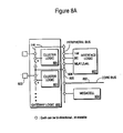
- FIG. 8 a is a block diagram illustration of an alternate embodiment and FIG. 8 b illustrates the embodiment incorporated into a dual port SRAM with a FPGA.
- the system of the present invention provides a flexible programmable bus structure system of lines to couple one or more circuits for input and output as well as to each other.
- numerous details are set forth in order to provide a thorough understanding of the present invention. However, it will be apparent to one skilled in the art that these specific details are not required in order to practice the present invention. In other instances, well known electrical structures and circuits are shown in block diagram form in order not to obscure the present invention unnecessarily.
- FIG. 2 One embodiment of the programmable bus system is illustrated in FIG. 2.
- the system is illustrated using a megacell circuit; however, it is readily apparent that the system can be utilized with a variety of types of circuits and/or components.
- the type of megacell component used in the following discussion is a 256 ⁇ 8 dual port static random access memory (SRAM).
- SRAM static random access memory
- the bus system described herein is not limited to SRAM components.
- a variety of components, such as microcontrollers, buffers, digital signal processors (DSPs) can be coupled to the bus system described herein.
- FIG. 2 illustrates one embodiment of the configurable bus system of the present invention.
- the configurable bus system of lines includes groups of lines 210 , lines 215 , and lines 220 , 225 .
- Each data input/output port of the megacell 205 is connected to one line of lines 210 .
- DI[0] is connected to Data[0]
- DI[1] is connected to Data[1], etc.
- each read or write address port of the megacell 205 is connected to one of the group of lines 215 .
- lines 225 are connected to the control ports of the megacell 205 .
- the exemplary system described herein has been programmed to convey address, data and control information across certain of the lines which form the bus system of lines. It is readily apparent that in other applications the system may only convey other combinations of information such as data and control.
- the lines are programmable and can be configured for a variety of types of information in addition to the types of information described herein.
- data is preferably input to the megacell 205 and output from the megacell through interface logic 230 .
- the interface logic is embodied in a programmable logic device, such as a field programmable gate array (FPGA); however, other types of logic can be used.
- a first set of programmable connections programmably couple the interface logic 230 to the data input/output ports of the megacell 205 (e.g., elements 235 , 240 , 245 , 250 ).
- programmable elements 235 , 240 selectively connect a first line 255 from the interface logic 230 to lines Data[0] 211 and Data[8] 212 .
- the programmable elements of the first set of programmable elements programmably couple the interface logic 230 to line 215 .
- programmable elements 237 , 247 selectively connect a first line 256 from the input/output logic 230 to bussed lines READA[0] 216 and WRITEA[0] 217 .
- the location of the programmable elements and the lines that each programmable element selectively connects to can be varied according to application.
- FIG. 2 illustrates one arrangement of programmable elements of the first set of programmable elements that provides flexibility in configuring the bus system of lines.
- the control signals to the megacell 205 can be similarly transmitted over the configurable bus system described herein.
- a second set of programmable connections are used to selectively connect control signals received from the interface logic 230 to the lines 225 and megacell 205 .
- programmable elements 261 , 262 selectively connect a global clock input to lines 226 , 227 .
- lines READA[8], READA[9], WRITEA[8], WRITEA[9] ( 220 collectively) are used to provide the higher order address bits as control inputs to select other coupled megacells. This illustrates the capability of this innovative bus system to provide system level integration.
- a third set of programmable connections are used to selectively extend the number of megacells coupled to the configurable bus system.
- the bus system is configurable using elements of the third set of programmable connections to selectively connect on or more megacells to the bus system of lines.
- the third set of programmable connections selectively limit the load on the lines for better performance by extending the lines (and therefore increasing the load) only when needed.
- programmable elements 270 , 271 selectively extend the lines 210 and lines 215 .
- the interface logic 230 is programmable and provides bidirectional access to the bus. In addition, it is preferably that the interface logic provides three-statable control to the bus. In particular, control bits and associated logic is used to provide bidirectional, three state control and selective input/output of a plurality of external connections to the lines of the bus system.
- the input/output logic 230 includes a plurality of elements, e.g., 231 , 232 , 233 , 234 . Each element is coupled to two external connections 280 , 281 . Each element is further coupled to enable control signals, e0 282 , e1 283 .
- the enable control signals e0 , e1 and control bits 284 , 285 function to provide the three state bus functionality that selects one of two external connections for input to or output from the bus.
- Control bit 284 controls the connection as input to the megacell 205 and control bit 285 controls the connection as output from the megacell 205 . If the control bit 284 is set to a first state, e.g., zero, the three-state connection is disabled. If the control bit 284 is set to a second state, e.g., 1, the state of the connection is controlled by enable control signals e0, e1.
- a first state e.g., zero
- the control bit 284 is set to a second state, e.g., 1, the state of the connection is controlled by enable control signals e0, e1.
- the present embodiment incorporates the bidirectional, three state access to the bus system of lines, it is contemplated that bidirectional three state access mechanism is implemented separate from the interface logic.
- the programming of the bus system of lines can be achieved a variety of ways. One method is to manually program the different programmable connections associated with particular lines of the bus system of lines. Other automated methods are also contemplated. Obviously, once programmed, the programmable connections can remain in the programmed state. Alternately, a dynamic programmable system can be provided wherein control circuitry coupled to the bus system and the programmable connections can determine, prior to a data transfer, those connections to program in order to configure the bus system of lines to transfer the data. This control circuitry could reside in a circuit coupled to the bus system for the transfer of data or in a circuit external to the bus system and connected circuits. For example, the bus system may couple a processor or arithmetic logic unit and memory. The processor or ALU can contain the control circuitry to configure the bus for each data transfer or plurality of transfers.
- connections to be programmed can be determined a variety of ways in order to configure the bus system for a general transfer or specific transfers of data.
- the control circuitry could examine the content of the data to be transferred and the control signals issued prior to or contemporaneous with a request to transfer or a signal indicating data is to be transferred (e.g., read or write signals or commands) to determine the programmable connections to be programmed.
- the bus system described can be used to connect components, logic circuits and the like which span across one or more elements.
- the bus system is used to connect memory (SRAM) to the logic of a programmable logic device (PLD) such as a field programmable gate array (FPGA).
- PLD programmable logic device
- FPGA field programmable gate array
- the bus system is used to integrate the memory into the same component as the FPGA.
- the FPGA embodied as the interface logic in the present embodiment, preferably functions as control logic for accessing the SRAM or as interface logic between the SRAM and other devices.
- a programmable logic device such as those described in U.S. Pat. No. 5,457,410 and U.S. patent application Ser. No. 08/534,500, filed Sep. 27, 1995 is used.
- FIG. 3 is a block diagram of an exemplary FPGA 300 .
- the I/O logic blocks 302 , 303 , 311 , and 312 provide an interface between external package pins of the FPGA 300 and the internal user logic either directly or through the I/O to Core interface 304 , 305 , 313 , 314 .
- the external package pins are coupled to the lines of bus system ( 210 , 215 , FIG. 2), the signals that are processed through the input/output logic ( 230 FIG. 2), and the ports of the megacell ( 205 , FIG. 2).
- Four interface blocks 304 , 305 , 313 and 314 provide decoupling between core 306 and logic 302 , 303 , 311 and 312 .
- the Core 306 includes configurable logic and an interconnect hierarchy.
- the logic is organized in a number of clusters 307 of logic which are intraconnected by an I-Matrix 301 and interconnected by MLA routing network 308 .
- the core also includes control/programming logic 309 to control the bits for programming the intraconnection and interconnection lines.
- SRAM technology is utilized.
- fuse or antifuse, EEPROM/ferroelectric or similar technology may be used.
- a separate clock/reset logic 310 is used to provide clock and reset lines on a group basis.
- FIG. 4 a is an example of a logic cluster. It is contemplated that the logic cluster illustrated by FIG. 4 a is illustrative and logic cluster can be formed of other elements such as logic gates and flip-flops. Referring to FIG. 4 a, the logic cluster 400 is formed of four logic elements. These elements include one 2 input combinational logic or configurable function generator (CFG) 402 , two three input CFGs 404 , 406 and D flip-flop 408 . CFG 402 can also be a three input CFG.
- CFG configurable function generator
- the CFGs 402 , 404 , 406 are programmable combinatorial logic that provide a predetermined output based using two input values (for CFG 402 ) or three input values (for CFGs 404 , 406 ).
- the CFGs are programmed with values to provide output representative of a desired logic function.
- the D flip flop 408 functions as a temporary storage element such as a register.
- This combination of one two input, one output CFG, two three input one output CFGs and a D flip flop enable a variety of logic and arithmetic functions to be performed.
- the elements can be programmed to perform such functions as comparator functions or accumulator functions. In the present embodiment, it is used to selectively couple bus signal lines to input/outputs of a megacell and to input/output logic.
- this combination of elements provides a fine granularity without the addition of redundant elements which add to the die size and speed of processing.
- the combination of elements also maximizes usage of elements thereby maximizing usage of die size space.
- the fine granularity characteristic resulting in more output points that can be tapped is a desirable characteristic as often an intermediate signal generated by a particular combination of elements is needed.
- the local interconnect within the cluster is structured to enable signals to be processed with minimum delays.
- the cluster elements, 402 , 404 , 406 , 408 are connected through interconnection lines I-M0 through I-M5 (referred to herein collectively as I-Matrix lines) which are oriented horizontally and vertically through the logic cluster.
- I-Matrix lines interconnection lines I-M0 through I-M5 (referred to herein collectively as I-Matrix lines) which are oriented horizontally and vertically through the logic cluster.
- These intraconnections of a cluster are programmable through switches, for example switches 420 - 444 .
- Intraconnections lines I-M0 to I-M5 and switches 420 - 444 form what is referred to herein as the I-Matrix.
- the I-Matrix provides connectability among the elements 402 , 404 , 406 , 408 to at least one other element of the cluster.
- the output of the CFG 202 can be connected to the input of CFG 404 by enabling switches 424 and 428 .
- switches 450 - 455 and connected lines provide such connections. It has been determined that the input and output of the three input CFGs 404 , 406 often perform programmed functions in conjunction with the register 408 . For example the three input CFGs can be utilized with the register to provide a one bit multiplexing function.
- the bi-directional switches 450 - 455 can be programmed a variety of ways to route the signal to achieve a specific function.
- a signal output by CFG 404 can drive D flip-flop 408 by enabling switch 451 .
- the signal may be driven onto the I-Matrix by enabling switch 450 .
- the output of CFG 406 can drive the input of the D flip-flop 408 by enabling switch 455 .
- Other routing paths by selectively enabling switches are also possible.
- the output of the CFG 402 can drive the D flip-flop 408 by an indirect connection through the I-Matrix. Thus, extreme flexibility is achieved.
- the routing of the output signal of the D flip-flop is also programmable through switches 452 and 453 .
- switches 452 or- 453 and selective switches of the I-Matrix the output signal can be routed to any one of the elements of the cluster or of other clusters.
- the signal output is selectively routed through the switches 433 - 435 adjacent to the CFG 204 or to switches 441 , 442 and 443 adjacent to CFG 406 . Die savings are achieved without decreasing the level of usage of elements in the device.
- Each logic cluster is connectable to the other logic clusters inside the logic block through switches extending the I-matrix between neighboring clusters.
- FIG. 4 b illustrates I-matrix interconnection lines I-M0 to I-M5 of a first logic cluster 460 selectively connected to the I-Matrix lines of adjacent logic clusters 461 and 463 , respectively through switches 464 , 465 , 466 , 467 , 475 and 476 .
- the switches can be implemented a variety of ways.
- the switches can be implemented as fusible links which are programmed by blowing the fuse to open or short the switch.
- the switch can be a passgate controlled by a bit in an SRAM array. The state of the bits in the array dictate whether a corresponding passgates are open or closed.
- FIG. 4 b illustrates the extensions of the I-Matrix within a logic cluster to neighboring clusters.
- switch 475 connects I-M5 of cluster 460 to I-M0 of cluster 461 and switch 476 connects I-M1 of cluster 460 to I-M2 of duster 461 .
- a plurality of interconnected logic clusters form a logic block.
- each logic block consists of four logic clusters organized in a 2 ⁇ 2 array as generally illustrated by FIG. 5 a.
- Each logic block has a set of bi-directional routing lines to which all CFGs inside the logic clusters are programmably connected.
- the bi-directional routing lines provide the path for signals to travel into and out of the logic block to the routing lines of a hierarchical routing architecture having multiple lengths of interconnections at different levels of the hierarchy.
- the block connectors can also provide connections among the CFGs of the logic clusters of the same block and adjacent blocks.
- each input and output of each element of each logic cluster of the logic block can be selectively connected to each block connector, to control the expansion on die size it is preferred that each input and output is selectively connected to a subset of block connectors.
- An example of such an embodiment is shown in FIG. 5 b.
- each element-of each cluster 500 e.g., CFG1, CFG2 and CFG3 is connected to two identified block connectors (BC) at the inputs.
- BC block connectors
- Two block connectors are identified as coupled to the output of the two input CFG1 and three block connectors are coupled to the output of the three input CFGs (CFG2, CFG3).
- the specific block connectors coupled to each elements are distributed among the elements of the block to maximize connectivity.
- the block connectors provide the input and output mechanism for interconnecting to higher levels of connections of the routing hierarchy referred to as the multiple level architecture (MLA) routing network.
- the network consists of multiple levels of routing lines (e.g., MLA-1, MLA-2, MLA-3, MLA-4, etc.) organized in a hierarchy wherein the higher level routing lines are a multiple longer than the lower level routing lines.
- MLA-2 routing lines are twice as long as MLA-1 routing lines
- MLA-3 routing lines are twice as long as MLA-2 routing lines
- MLA-4 routing lines are twice as long as MLA-3 routing lines.
- the user can program the PLD and the bus to access the memory in a variety of configurations without requiring significant space on the component.
- FIG. 6 shows the bus system configured to couple to 4 SRAM megacells arranged in a 2 ⁇ 2 configuration.
- the programmable elements are configured as passgates controlled by a bit in one of the SRAMs or other coupled memory.
- no extra logic or interconnect is required for the bus system configuration.
- the bus system is easily configured for the particular arrangement of megacells.
- the bus system is programmed to be coupled to the interconnect of the PLD (e.g., block connectors (bc), I-matrix lines (IM) and MLA lines (MLA-1)) to enable the logic of the PLD to provide the necessary interface logic to interface the SRAM to components or devices external to the system.
- the PLD provides logic to assert the necessary control signals to transmit the address information and receive and transmit data.
- data and address information is communicated through the bi-directional block connectors.
- Control information including control signals to control the state of the enable signals (e0, e1) are communicated via the I-matrix and MLA-1 lines.
- FIG. 7 a is a block diagram illustration of one embodiment of megacell 701 , 702 , coupled to the bus system of the present invention.
- a program controlled interface 703 , 704 to the bus system of lines 705 and megacells 701 , 702 are provided.
- the interface from the core bus 705 to the I/O 706 , 707 can be achieved using hardwired or program controlled connections 708 , 709 .
- these connections are achieved using a programmable, peripheral bus system of lines 710 , 711 to provide further flexibility.
- the peripheral bus system is preferably programmable in the same manner as described above with respect to FIG. 2.
- the interface logic ( 230 FIG. 2) provides the program controlled interface 703 , 704 to the bus system 705 which is also programmed controlled.
- FIG. 7 b depicts an overview of an exemplary component configured with dual port SRAM megacells and a FPGA.
- the FPGA including its interconnect structure, is represented by elements 712 , 715 , 720 , 725 .
- Each element 712 , 715 , 720 , 725 comprises a plurality of logical blocks organized in 16 ⁇ 16 array with a corresponding hierarchical interconnect structure as discussed in U.S. Pat. No. 5,457,410 and U.S. patent application Ser. No. 08/534,500.
- the FPGA elements 712 , 715 , 720 , 725 are connected by the interconnect, e.g., block connectors, I-matrix lines and MLA lines (see FIG.
- bus system preferably spans the entire component to the adjacent array of SRAMs 775 , 780 , 785 , 790 through programmable elements (not shown).
- the bus system is further coupled to I/O ports or pads (e.g., 791 , 792 ) for input/output to/from the system to external components or devices.
- the bus system can be coupled through hardwired connections, it is preferred that the connection be made via programmable elements, e.g., 765 , 770 and bus system of lines 775 .
- FIG. 8 a is a block diagram illustration of an alternate embodiment in which gateway interface logic 801 is used to interface the core bus system 802 to the I/O 803 .
- this diagram illustrates alternative programmable connections that can be implemented to provide further programmability and flexibility to the system.
- the gateway interface logic 800 is composed of hardwired logic, metal programmable logic, or programmable logic such as a plurality of logic clusters and is directly or indirectly coupled (i.e., direct hardwired connections or indirect program controlled connections) to the megacell 804 .
- FIG. 8 a shows the gateway interface logic 800 is coupled to the megacell 804 via peripheral bus 805 which preferably includes bidirectional, three-statable connections (e.g., 808 ).
- the gateway interface logic 800 provides an additional level of logic to the interface between the megacell and the I/O pads or ports to external components or devices.
- the gateway interface logic can enable faster transfer of information.
- the gateway interface logic can be structured to provide the specific bus protocols or handshaking required to interface to external devices.
- the gateway interface logic can also provide address decode functionality (e.g., wide decode) to expedite processing of information.
- the gateway interface logic 800 is implemented as a logic cluster 801 , consistent with the logic clusters referred to herein and in U.S. Pat. No. 5,457,410 and U.S. patent application Ser. No. 08/534,500. I-Matrix lines are used to connect the gateway logic to the peripheral bus 805 . It should be recognized that the gateway interface logic is not limited to the specific implementation described herein and a variety of logic implementations can be used.
- FIG. 8 b illustrates dual port SRAMs with FPGA and the configurable bus system.
- further programmability is provided at the I/O ports of the system using gateway interface logic.
- the programmable gateway logic e.g., 830
- the core bus system of lines e.g., elements 810 , 815 , 820
- the I/O e.g., 825
- a logic cluster as illustrated in FIG. 4 a is used; however, as noted above, it is contemplated that other forms of logic can be utilized.
- this embodiment includes a peripheral bus system of lines 840 , which functions is a manner similar to the core bus system of lines providing a programmable bus system for transferring information.
- each of the programmable connections of the bus system e.g., 846 , 847
- programmable connections from the core bus (e.g., 820 ) direct to the peripheral bus 840 and from the megacell (e.g., 845 ) direct to the peripheral bus 840 .
- programmable connection 822 selectively enables the bus element 820 to be connected to peripheral bus 840 .
- programmable element 824 selectively connects megacell 845 directly to peripheral bus 840 .
- Such flexibility is advantageous when speed is a consideration. For example, it may be desirable to directly connect externally received control input data to the megacell.
Abstract
Description
- This application is a continuation of U.S. application Ser. No. 10/231,320 filed Aug. 28, 2002, which is a continuation of U.S. application Ser. No. 09/960,916 filed Sep. 24, 2001, U.S. Pat. No. 6,504,399, which is a continuation of U.S. application Ser. No. 09/243,998 filed Feb. 4, 1999, U.S. Pat. No. 6,329,839, which is a continuation of U.S. application Ser. No. 08/708,403 filed Sep. 4, 1996, U.S. Pat. No. 6,034,547.
- 1. Field of the Invention
- The present invention is directed to a programmable, configurable bus system of liens to interconnect electrical components for an electrical/electronics system.
- 2. Art Background
- Megacells are described as block components such as static random access memory (SRAM), microcontrollers, microprocessors and buffers. Sometimes it is desirable to interconnect a plurality of megacells together to provide a larger functional entity. One way to interconnect multiple megacells and logic circuits is through a hardwired bus system. Examples are illustrated in FIGS. 1 a, 1 b and 1 c. FIG. 1a illustrates a bus interface to a dual port SRAM megacell. Bus lines include DATA 0-DATA15, READA0-READA9, WRITEA0-WRITEA9. To couple multiple megacells, the data lines are shared among the coupled cells. However, separate read and write lines would be required for each megacell. To the contrary, if the megacells were coupled to generate a deeper combined megacell, the data lines would be separate for each megacell and the read and write lines would be shared among the megacells. Control signals are then be used to select a particular megacell for a particular operation. This is illustrated in FIGS. 1b and 1 c.
- Such configurations are hardwired and cannot easily be changed to accommodate different configurations. Furthermore, if errors occur in the mask generated, repairs are not easily made, as configurability is minimal. In addition to providing a bus system to interconnect multiple megacells, tristatable input ports are sometimes used to enable multiple inputs to be input to a particular bus line thus allowing a system level communication between logic to megacells or megacells to megacells. However, a single tristate can directly couple to only one line.
- The system and method of the present invention provides an innovative bus system of lines which can be programmed to provide data, control and address information to the logic circuits interconnected by the bus system in the context of an electrical/electronics system. This flexible structure and process enables a configurable system to be created to programmably connect one or more logic circuits such as megacells to external logic devices and other megacells. Thus, a system can be built using the bus structure of lines by selectively coupling the input signals and output signals from the logic circuits. The programmability of the bus system enables the cascading of multiple megacells in an arbitrary fashion (i.e., wide, deep or both) and the sharing of common lines for system level communication.
- In one embodiment, a plurality of bussed lines are coupled to the data ports of megacells. A first set of programmable logic is coupled to selective lines of the system of lines and interface logic. The interface logic is coupled to input/output pads of the component for receipt of external input and output of data to be output external to the component. Individual elements of the first set of logic are programmed to selectively couple a particular interface logic element to a particular line and data port to enable the input and output of data to the megacell. It is preferred that, selective lines of the bus system of lines are each coupled to control ports of the megacell and a second set of programmable logic is coupled to the plurality of lines and interface logic elements to selectively couple a particular interface logic element to a particular line and control port to enable the selective input of control data. In another embodiment, the interface logic includes a plurality of programmable three state bi-directional input/out logic, each three state bi-directional input/output logic element coupled to the first set of programmable logic to provide further programmability to selectively couple one of the two external input or output to one of a plurality of the lines of the bus system.
- In another embodiment, gateway logic is provided as coupled between the I/O pads and the processing logic. The interface logic can be configured to provide communication enhancements, such as protocols and the like, to enable sophisticated communications to and from the megacells through the bus system thus allowing a flexible scheme of a system on a chip having a bus system.
- In other embodiments, programmable connections are provided between the I/O pads and the megacells and between the gateway logic and the megacells.
- In addition, the programmable bus structure enables multiple megacells to be coupled together simply by programming the first set of programmable logic, second set of programmable logic and a third set of programmable logic which selectively extends the lines used to convey data, address and control information to additional megacells. This structure therefore enables additional megacells to be coupled without the prior art limitations of hardwiring connections and adding megacells in either the horizontal (width-wise) or vertical (depth-wise) orientation. Furthermore, the system allows the sharing of a common system bus for communicating among megacells.
- The objects, features and advantages of the present invention will be apparent to one skilled in the art from the following detailed description in which:
- FIGS. 1 a, 1 b and 1 c illustrate interconnections of prior art megacells.
- FIG. 2 illustrates one embodiment in which logic is programmably coupled to the megacell.
- FIG. 3 is a block diagram illustration of exemplary programmable-logic utilized to implement one embodiment of the configurable bus system of the present invention.
- FIGS. 4A and 4B illustrate the organization of the programmable logic of FIG. 3.
- FIGS. 5A and 5B provide further illustration of the organization of the programmable logic of FIG. 3.
- FIG. 6 illustrates the programmability of connections to bussed signal lines to multiple megacells in accordance with the teachings of the present invention.
- FIG. 7 a is a block diagram illustration of one embodiment of a megacell connected to the bus system and I/O.
- FIG. 7 b illustrates one embodiment of a dual-port static random access memory (SRAM) megacell with a field programmable gate array (FPGA).
- FIG. 8 a is a block diagram illustration of an alternate embodiment and FIG. 8b illustrates the embodiment incorporated into a dual port SRAM with a FPGA.
- The system of the present invention provides a flexible programmable bus structure system of lines to couple one or more circuits for input and output as well as to each other. In the following description, for purposes of explanation, numerous details are set forth in order to provide a thorough understanding of the present invention. However, it will be apparent to one skilled in the art that these specific details are not required in order to practice the present invention. In other instances, well known electrical structures and circuits are shown in block diagram form in order not to obscure the present invention unnecessarily.
- One embodiment of the programmable bus system is illustrated in FIG. 2. The system is illustrated using a megacell circuit; however, it is readily apparent that the system can be utilized with a variety of types of circuits and/or components. The type of megacell component used in the following discussion is a 256×8 dual port static random access memory (SRAM). However, the bus system described herein is not limited to SRAM components. A variety of components, such as microcontrollers, buffers, digital signal processors (DSPs) can be coupled to the bus system described herein.
- FIG. 2 illustrates one embodiment of the configurable bus system of the present invention. Referring to FIG. 2, the configurable bus system of lines includes groups of
lines 210,lines 215, andlines 220, 225. Each data input/output port of themegacell 205 is connected to one line oflines 210. For example, DI[0] is connected to Data[0], DI[1] is connected to Data[1], etc. In addition, each read or write address port of themegacell 205 is connected to one of the group oflines 215. Furthermore, lines 225 are connected to the control ports of themegacell 205. It is recognized that the exemplary system described herein has been programmed to convey address, data and control information across certain of the lines which form the bus system of lines. It is readily apparent that in other applications the system may only convey other combinations of information such as data and control. In addition, one skilled in the art recognizes that the lines are programmable and can be configured for a variety of types of information in addition to the types of information described herein. - In the present embodiment, data is preferably input to the
megacell 205 and output from the megacell throughinterface logic 230. As will be described below, the interface logic is embodied in a programmable logic device, such as a field programmable gate array (FPGA); however, other types of logic can be used. A first set of programmable connections programmably couple theinterface logic 230 to the data input/output ports of the megacell 205 (e.g.,elements programmable elements 235, 240 selectively connect afirst line 255 from theinterface logic 230 to lines Data[0] 211 and Data[8] 212. In addition, in the present embodiment, the programmable elements of the first set of programmable elements programmably couple theinterface logic 230 toline 215. For example,programmable elements 237, 247 selectively connect afirst line 256 from the input/output logic 230 to bussed lines READA[0] 216 and WRITEA[0] 217. Furthermore, the location of the programmable elements and the lines that each programmable element selectively connects to can be varied according to application. FIG. 2 illustrates one arrangement of programmable elements of the first set of programmable elements that provides flexibility in configuring the bus system of lines. - The control signals to the
megacell 205 can be similarly transmitted over the configurable bus system described herein. A second set of programmable connections are used to selectively connect control signals received from theinterface logic 230 to the lines 225 andmegacell 205. For example,programmable elements lines - Preferably, a third set of programmable connections are used to selectively extend the number of megacells coupled to the configurable bus system. The bus system is configurable using elements of the third set of programmable connections to selectively connect on or more megacells to the bus system of lines. The third set of programmable connections selectively limit the load on the lines for better performance by extending the lines (and therefore increasing the load) only when needed. In the present embodiment, for example, programmable elements 270, 271 selectively extend the
lines 210 andlines 215. - In addition, it is preferred that the
interface logic 230 is programmable and provides bidirectional access to the bus. In addition, it is preferably that the interface logic provides three-statable control to the bus. In particular, control bits and associated logic is used to provide bidirectional, three state control and selective input/output of a plurality of external connections to the lines of the bus system. Referring to FIG. 2, the input/output logic 230 includes a plurality of elements, e.g., 231, 232, 233, 234. Each element is coupled to twoexternal connections e0 282,e1 283. The enable control signals e0 , e1 and controlbits Control bit 284 controls the connection as input to themegacell 205 and control bit 285 controls the connection as output from themegacell 205. If thecontrol bit 284 is set to a first state, e.g., zero, the three-state connection is disabled. If thecontrol bit 284 is set to a second state, e.g., 1, the state of the connection is controlled by enable control signals e0, e1. Although the present embodiment incorporates the bidirectional, three state access to the bus system of lines, it is contemplated that bidirectional three state access mechanism is implemented separate from the interface logic. - The programming of the bus system of lines can be achieved a variety of ways. One method is to manually program the different programmable connections associated with particular lines of the bus system of lines. Other automated methods are also contemplated. Obviously, once programmed, the programmable connections can remain in the programmed state. Alternately, a dynamic programmable system can be provided wherein control circuitry coupled to the bus system and the programmable connections can determine, prior to a data transfer, those connections to program in order to configure the bus system of lines to transfer the data. This control circuitry could reside in a circuit coupled to the bus system for the transfer of data or in a circuit external to the bus system and connected circuits. For example, the bus system may couple a processor or arithmetic logic unit and memory. The processor or ALU can contain the control circuitry to configure the bus for each data transfer or plurality of transfers.
- Furthermore, it is contemplated that the connections to be programmed can be determined a variety of ways in order to configure the bus system for a general transfer or specific transfers of data. For example, the control circuitry could examine the content of the data to be transferred and the control signals issued prior to or contemporaneous with a request to transfer or a signal indicating data is to be transferred (e.g., read or write signals or commands) to determine the programmable connections to be programmed.
- The bus system described can be used to connect components, logic circuits and the like which span across one or more elements. In the present example, as noted above, the bus system is used to connect memory (SRAM) to the logic of a programmable logic device (PLD) such as a field programmable gate array (FPGA). More particularly, in the present embodiment, the bus system is used to integrate the memory into the same component as the FPGA. The FPGA, embodied as the interface logic in the present embodiment, preferably functions as control logic for accessing the SRAM or as interface logic between the SRAM and other devices. Preferably, a programmable logic device such as those described in U.S. Pat. No. 5,457,410 and U.S. patent application Ser. No. 08/534,500, filed Sep. 27, 1995 is used.
- FIG. 3 is a block diagram of an
exemplary FPGA 300. The I/O logic blocks 302, 303, 311, and 312 provide an interface between external package pins of theFPGA 300 and the internal user logic either directly or through the I/O toCore interface core 306 andlogic - The
Core 306 includes configurable logic and an interconnect hierarchy. In the present embodiment, the logic is organized in a number ofclusters 307 of logic which are intraconnected by an I-Matrix 301 and interconnected byMLA routing network 308. The core also includes control/programming logic 309 to control the bits for programming the intraconnection and interconnection lines. In the embodiment described herein, SRAM technology is utilized. However, fuse or antifuse, EEPROM/ferroelectric or similar technology may be used. In order to minimize skewing, a separate clock/reset logic 310 is used to provide clock and reset lines on a group basis. - The present embodiment provides logic in groups called clusters. FIG. 4 a is an example of a logic cluster. It is contemplated that the logic cluster illustrated by FIG. 4a is illustrative and logic cluster can be formed of other elements such as logic gates and flip-flops. Referring to FIG. 4a, the
logic cluster 400 is formed of four logic elements. These elements include one 2 input combinational logic or configurable function generator (CFG) 402, two threeinput CFGs flop 408.CFG 402 can also be a three input CFG. TheCFGs CFGs 404, 406). The CFGs are programmed with values to provide output representative of a desired logic function. TheD flip flop 408 functions as a temporary storage element such as a register. - This combination of one two input, one output CFG, two three input one output CFGs and a D flip flop enable a variety of logic and arithmetic functions to be performed. For example, the elements can be programmed to perform such functions as comparator functions or accumulator functions. In the present embodiment, it is used to selectively couple bus signal lines to input/outputs of a megacell and to input/output logic. It should be noted that this combination of elements provides a fine granularity without the addition of redundant elements which add to the die size and speed of processing. Furthermore, the combination of elements also maximizes usage of elements thereby maximizing usage of die size space. The fine granularity characteristic resulting in more output points that can be tapped is a desirable characteristic as often an intermediate signal generated by a particular combination of elements is needed.
- In addition, the local interconnect within the cluster is structured to enable signals to be processed with minimum delays. The cluster elements, 402, 404, 406, 408, are connected through interconnection lines I-M0 through I-M5 (referred to herein collectively as I-Matrix lines) which are oriented horizontally and vertically through the logic cluster. These intraconnections of a cluster are programmable through switches, for example switches 420-444. Intraconnections lines I-M0 to I-M5 and switches 420-444 form what is referred to herein as the I-Matrix. The I-Matrix provides connectability among the
elements CFG 404 by enablingswitches - To ensure minimum signal delays during processing, separate, direct connections are provided between the
D flip flop 408 and the threeinput CFGs input CFGs register 408. For example the three input CFGs can be utilized with the register to provide a one bit multiplexing function. - The bi-directional switches 450-455 can be programmed a variety of ways to route the signal to achieve a specific function. For example, a signal output by
CFG 404 can drive D flip-flop 408 by enablingswitch 451. Altemately, the signal may be driven onto the I-Matrix by enablingswitch 450. Similarly, the output ofCFG 406 can drive the input of the D flip-flop 408 by enablingswitch 455. Other routing paths by selectively enabling switches are also possible. Furthermore, the output of theCFG 402 can drive the D flip-flop 408 by an indirect connection through the I-Matrix. Thus, extreme flexibility is achieved. - The routing of the output signal of the D flip-flop is also programmable through
switches switches 452 or-453 and selective switches of the I-Matrix, the output signal can be routed to any one of the elements of the cluster or of other clusters. The signal output is selectively routed through the switches 433-435 adjacent to the CFG 204 or toswitches CFG 406. Die savings are achieved without decreasing the level of usage of elements in the device. - Each logic cluster is connectable to the other logic clusters inside the logic block through switches extending the I-matrix between neighboring clusters. FIG. 4 b illustrates I-matrix interconnection lines I-M0 to I-M5 of a
first logic cluster 460 selectively connected to the I-Matrix lines ofadjacent logic clusters 461 and 463, respectively throughswitches - The flexibility herein described is partially achieved through the numerous bi-directional switches used. It was also noted previously that the switches can be implemented a variety of ways. For example, the switches can be implemented as fusible links which are programmed by blowing the fuse to open or short the switch. Alternately, the switch can be a passgate controlled by a bit in an SRAM array. The state of the bits in the array dictate whether a corresponding passgates are open or closed.
- To allow an efficient implementation of a carry chain as well as other applications, staggered or barrel connections between clusters is used to increased connectivity. FIG. 4 b illustrates the extensions of the I-Matrix within a logic cluster to neighboring clusters. For example, switch 475 connects I-M5 of
cluster 460 to I-M0 ofcluster 461 and switch 476 connects I-M1 ofcluster 460 to I-M2 ofduster 461. - A plurality of interconnected logic clusters form a logic block. In the present embodiment each logic block consists of four logic clusters organized in a 2×2 array as generally illustrated by FIG. 5 a. Each logic block has a set of bi-directional routing lines to which all CFGs inside the logic clusters are programmably connected. The bi-directional routing lines provide the path for signals to travel into and out of the logic block to the routing lines of a hierarchical routing architecture having multiple lengths of interconnections at different levels of the hierarchy. It can also be seen that the block connectors can also provide connections among the CFGs of the logic clusters of the same block and adjacent blocks. Although the input and output of each element of each logic cluster of the logic block can be selectively connected to each block connector, to control the expansion on die size it is preferred that each input and output is selectively connected to a subset of block connectors. An example of such an embodiment is shown in FIG. 5b.
- Referring to FIG. 5 b, a symbolic representation of one embodiment of the connections to block connectors within a
block 300 is shown. Each element-of eachcluster 500, e.g., CFG1, CFG2 and CFG3 is connected to two identified block connectors (BC) at the inputs. Two block connectors are identified as coupled to the output of the two input CFG1 and three block connectors are coupled to the output of the three input CFGs (CFG2, CFG3). The specific block connectors coupled to each elements are distributed among the elements of the block to maximize connectivity. - The block connectors provide the input and output mechanism for interconnecting to higher levels of connections of the routing hierarchy referred to as the multiple level architecture (MLA) routing network. The network consists of multiple levels of routing lines (e.g., MLA-1, MLA-2, MLA-3, MLA-4, etc.) organized in a hierarchy wherein the higher level routing lines are a multiple longer than the lower level routing lines. For example, MLA-2 routing lines are twice as long as MLA-1 routing lines and MLA-3 routing lines are twice as long as MLA-2 routing lines and MLA-4 routing lines are twice as long as MLA-3 routing lines.
- Using the logic and interconnect hierarchy described, the user can program the PLD and the bus to access the memory in a variety of configurations without requiring significant space on the component.
- The flexibility and utility of the configurable bus system of the present invention is illustrated with reference to FIG. 6. FIG. 6 shows the bus system configured to couple to 4 SRAM megacells arranged in a 2×2 configuration. The programmable elements are configured as passgates controlled by a bit in one of the SRAMs or other coupled memory. As is illustrated, no extra logic or interconnect is required for the bus system configuration. By enablement of the proper links which control the interconnect, the bus system is easily configured for the particular arrangement of megacells.
- In the present example, the bus system is programmed to be coupled to the interconnect of the PLD (e.g., block connectors (bc), I-matrix lines (IM) and MLA lines (MLA-1)) to enable the logic of the PLD to provide the necessary interface logic to interface the SRAM to components or devices external to the system. For example, the PLD provides logic to assert the necessary control signals to transmit the address information and receive and transmit data. In the example shown in FIG. 6, data and address information is communicated through the bi-directional block connectors. Control information, including control signals to control the state of the enable signals (e0, e1) are communicated via the I-matrix and MLA-1 lines.
- FIG. 7 a is a block diagram illustration of one embodiment of
megacell megacells O 706, 707 can be achieved using hardwired or program controlledconnections lines - FIG. 7 b depicts an overview of an exemplary component configured with dual port SRAM megacells and a FPGA. The FPGA, including its interconnect structure, is represented by
elements element FPGA elements elements SRAM elements SRAMs lines 775. - FIG. 8 a is a block diagram illustration of an alternate embodiment in which
gateway interface logic 801 is used to interface thecore bus system 802 to the I/O 803. In addition, this diagram illustrates alternative programmable connections that can be implemented to provide further programmability and flexibility to the system. - The
gateway interface logic 800 is composed of hardwired logic, metal programmable logic, or programmable logic such as a plurality of logic clusters and is directly or indirectly coupled (i.e., direct hardwired connections or indirect program controlled connections) to themegacell 804. FIG. 8a shows thegateway interface logic 800 is coupled to themegacell 804 viaperipheral bus 805 which preferably includes bidirectional, three-statable connections (e.g., 808). Thegateway interface logic 800 provides an additional level of logic to the interface between the megacell and the I/O pads or ports to external components or devices. The gateway interface logic can enable faster transfer of information. For example, the gateway interface logic can be structured to provide the specific bus protocols or handshaking required to interface to external devices. The gateway interface logic can also provide address decode functionality (e.g., wide decode) to expedite processing of information. - In the present embodiment, the
gateway interface logic 800 is implemented as alogic cluster 801, consistent with the logic clusters referred to herein and in U.S. Pat. No. 5,457,410 and U.S. patent application Ser. No. 08/534,500. I-Matrix lines are used to connect the gateway logic to theperipheral bus 805. It should be recognized that the gateway interface logic is not limited to the specific implementation described herein and a variety of logic implementations can be used. - FIG. 8 b illustrates dual port SRAMs with FPGA and the configurable bus system. In this embodiment, further programmability is provided at the I/O ports of the system using gateway interface logic. In particular, the programmable gateway logic (e.g., 830) is located between the core bus system of lines (e.g.,
elements lines 840, which functions is a manner similar to the core bus system of lines providing a programmable bus system for transferring information. Preferably, each of the programmable connections of the bus system (e.g., 846, 847) are bidirectional, three-statable connections. - Further enhancements and interconnect flexibility is achieved by providing programmable connections from the core bus (e.g., 820) direct to the
peripheral bus 840 and from the megacell (e.g., 845) direct to theperipheral bus 840. For example,programmable connection 822 selectively enables thebus element 820 to be connected toperipheral bus 840. Similarly,programmable element 824 selectively connects megacell 845 directly toperipheral bus 840. Such flexibility is advantageous when speed is a consideration. For example, it may be desirable to directly connect externally received control input data to the megacell. - The invention has been described in conjunction with the preferred embodiment. It is evident that numerous alternatives, modifications, variations and uses will be apparent to those skilled in the art in light of the foregoing description.
Claims (92)
Priority Applications (6)
| Application Number | Priority Date | Filing Date | Title |
|---|---|---|---|
| US10/412,975 US6781410B2 (en) | 1996-09-04 | 2003-04-11 | Method and apparatus for universal program controlled bus architecture |
| US10/811,422 US6975138B2 (en) | 1996-09-04 | 2004-03-25 | Method and apparatus for universal program controlled bus architecture |
| US11/219,597 US7382156B2 (en) | 1996-09-04 | 2005-09-01 | Method and apparatus for universal program controlled bus architecture |
| US12/148,071 US20080191739A1 (en) | 1996-09-04 | 2008-04-15 | Method and apparatus for universal program controlled bus architecture |
| US12/401,055 US7830173B2 (en) | 1996-09-04 | 2009-03-10 | Method and apparatus for universal program controlled bus architecture |
| US12/915,454 US7915918B2 (en) | 1996-09-04 | 2010-10-29 | Method and apparatus for universal program controlled bus architecture |
Applications Claiming Priority (5)
| Application Number | Priority Date | Filing Date | Title |
|---|---|---|---|
| US08/708,403 US6034547A (en) | 1996-09-04 | 1996-09-04 | Method and apparatus for universal program controlled bus |
| US09/243,998 US6329839B1 (en) | 1996-09-04 | 1999-02-04 | Method and apparatus for universal program controlled bus architecture |
| US09/960,916 US6504399B2 (en) | 1996-09-04 | 2001-09-24 | Method and apparatus for universal program controlled bus architecture |
| US10/231,320 US6624658B2 (en) | 1999-02-04 | 2002-08-28 | Method and apparatus for universal program controlled bus architecture |
| US10/412,975 US6781410B2 (en) | 1996-09-04 | 2003-04-11 | Method and apparatus for universal program controlled bus architecture |
Related Parent Applications (1)
| Application Number | Title | Priority Date | Filing Date |
|---|---|---|---|
| US10/231,320 Continuation US6624658B2 (en) | 1996-09-04 | 2002-08-28 | Method and apparatus for universal program controlled bus architecture |
Related Child Applications (1)
| Application Number | Title | Priority Date | Filing Date |
|---|---|---|---|
| US10/811,422 Continuation US6975138B2 (en) | 1996-09-04 | 2004-03-25 | Method and apparatus for universal program controlled bus architecture |
Publications (2)
| Publication Number | Publication Date |
|---|---|
| US20030197527A1 true US20030197527A1 (en) | 2003-10-23 |
| US6781410B2 US6781410B2 (en) | 2004-08-24 |
Family
ID=26936249
Family Applications (4)
| Application Number | Title | Priority Date | Filing Date |
|---|---|---|---|
| US10/231,320 Expired - Fee Related US6624658B2 (en) | 1996-09-04 | 2002-08-28 | Method and apparatus for universal program controlled bus architecture |
| US10/412,975 Expired - Lifetime US6781410B2 (en) | 1996-09-04 | 2003-04-11 | Method and apparatus for universal program controlled bus architecture |
| US10/811,422 Expired - Fee Related US6975138B2 (en) | 1996-09-04 | 2004-03-25 | Method and apparatus for universal program controlled bus architecture |
| US11/219,597 Expired - Fee Related US7382156B2 (en) | 1996-09-04 | 2005-09-01 | Method and apparatus for universal program controlled bus architecture |
Family Applications Before (1)
| Application Number | Title | Priority Date | Filing Date |
|---|---|---|---|
| US10/231,320 Expired - Fee Related US6624658B2 (en) | 1996-09-04 | 2002-08-28 | Method and apparatus for universal program controlled bus architecture |
Family Applications After (2)
| Application Number | Title | Priority Date | Filing Date |
|---|---|---|---|
| US10/811,422 Expired - Fee Related US6975138B2 (en) | 1996-09-04 | 2004-03-25 | Method and apparatus for universal program controlled bus architecture |
| US11/219,597 Expired - Fee Related US7382156B2 (en) | 1996-09-04 | 2005-09-01 | Method and apparatus for universal program controlled bus architecture |
Country Status (1)
| Country | Link |
|---|---|
| US (4) | US6624658B2 (en) |
Families Citing this family (85)
| Publication number | Priority date | Publication date | Assignee | Title |
|---|---|---|---|---|
| US7266725B2 (en) | 2001-09-03 | 2007-09-04 | Pact Xpp Technologies Ag | Method for debugging reconfigurable architectures |
| DE19651075A1 (en) | 1996-12-09 | 1998-06-10 | Pact Inf Tech Gmbh | Unit for processing numerical and logical operations, for use in processors (CPU's), multi-computer systems, data flow processors (DFP's), digital signal processors (DSP's) or the like |
| DE19654595A1 (en) | 1996-12-20 | 1998-07-02 | Pact Inf Tech Gmbh | I0 and memory bus system for DFPs as well as building blocks with two- or multi-dimensional programmable cell structures |
| EP1329816B1 (en) | 1996-12-27 | 2011-06-22 | Richter, Thomas | Method for automatic dynamic unloading of data flow processors (dfp) as well as modules with bidimensional or multidimensional programmable cell structures (fpgas, dpgas or the like) |
| US6542998B1 (en) | 1997-02-08 | 2003-04-01 | Pact Gmbh | Method of self-synchronization of configurable elements of a programmable module |
| US8686549B2 (en) | 2001-09-03 | 2014-04-01 | Martin Vorbach | Reconfigurable elements |
| DE19861088A1 (en) | 1997-12-22 | 2000-02-10 | Pact Inf Tech Gmbh | Repairing integrated circuits by replacing subassemblies with substitutes |
| JP2003505753A (en) | 1999-06-10 | 2003-02-12 | ペーアーツェーテー インフォルマツィオーンステヒノロギー ゲゼルシャフト ミット ベシュレンクテル ハフツング | Sequence division method in cell structure |
| DE50115584D1 (en) | 2000-06-13 | 2010-09-16 | Krass Maren | PIPELINE CT PROTOCOLS AND COMMUNICATION |
| US8058899B2 (en) | 2000-10-06 | 2011-11-15 | Martin Vorbach | Logic cell array and bus system |
| US9037807B2 (en) | 2001-03-05 | 2015-05-19 | Pact Xpp Technologies Ag | Processor arrangement on a chip including data processing, memory, and interface elements |
| US7844796B2 (en) | 2001-03-05 | 2010-11-30 | Martin Vorbach | Data processing device and method |
| US7444531B2 (en) | 2001-03-05 | 2008-10-28 | Pact Xpp Technologies Ag | Methods and devices for treating and processing data |
| US7996827B2 (en) | 2001-08-16 | 2011-08-09 | Martin Vorbach | Method for the translation of programs for reconfigurable architectures |
| US7434191B2 (en) | 2001-09-03 | 2008-10-07 | Pact Xpp Technologies Ag | Router |
| US8686475B2 (en) | 2001-09-19 | 2014-04-01 | Pact Xpp Technologies Ag | Reconfigurable elements |
| AU2003214003A1 (en) | 2002-02-18 | 2003-09-09 | Pact Xpp Technologies Ag | Bus systems and method for reconfiguration |
| US8914590B2 (en) | 2002-08-07 | 2014-12-16 | Pact Xpp Technologies Ag | Data processing method and device |
| US6781408B1 (en) | 2002-04-24 | 2004-08-24 | Altera Corporation | Programmable logic device with routing channels |
| US7142011B1 (en) | 2002-04-24 | 2006-11-28 | Altera Corporation | Programmable logic device with routing channels |
| US7657861B2 (en) | 2002-08-07 | 2010-02-02 | Pact Xpp Technologies Ag | Method and device for processing data |
| WO2005010632A2 (en) * | 2003-06-17 | 2005-02-03 | Pact Xpp Technologies Ag | Data processing device and method |
| AU2003286131A1 (en) | 2002-08-07 | 2004-03-19 | Pact Xpp Technologies Ag | Method and device for processing data |
| EP1537486A1 (en) | 2002-09-06 | 2005-06-08 | PACT XPP Technologies AG | Reconfigurable sequencer structure |
| DE112004000026D2 (en) * | 2003-04-04 | 2006-06-14 | Pact Xpp Technologies Ag | Method and device for data processing |
| EP1676208A2 (en) | 2003-08-28 | 2006-07-05 | PACT XPP Technologies AG | Data processing device and method |
| US8620980B1 (en) | 2005-09-27 | 2013-12-31 | Altera Corporation | Programmable device with specialized multiplier blocks |
| EP1974265A1 (en) | 2006-01-18 | 2008-10-01 | PACT XPP Technologies AG | Hardware definition method |
| US7423453B1 (en) * | 2006-01-20 | 2008-09-09 | Advantage Logic, Inc. | Efficient integrated circuit layout scheme to implement a scalable switching network used in interconnection fabric |
| US8266198B2 (en) | 2006-02-09 | 2012-09-11 | Altera Corporation | Specialized processing block for programmable logic device |
| US8266199B2 (en) | 2006-02-09 | 2012-09-11 | Altera Corporation | Specialized processing block for programmable logic device |
| US8301681B1 (en) | 2006-02-09 | 2012-10-30 | Altera Corporation | Specialized processing block for programmable logic device |
| US8041759B1 (en) | 2006-02-09 | 2011-10-18 | Altera Corporation | Specialized processing block for programmable logic device |
| US7836117B1 (en) | 2006-04-07 | 2010-11-16 | Altera Corporation | Specialized processing block for programmable logic device |
| US7822799B1 (en) | 2006-06-26 | 2010-10-26 | Altera Corporation | Adder-rounder circuitry for specialized processing block in programmable logic device |
| US8386550B1 (en) | 2006-09-20 | 2013-02-26 | Altera Corporation | Method for configuring a finite impulse response filter in a programmable logic device |
| US7930336B2 (en) | 2006-12-05 | 2011-04-19 | Altera Corporation | Large multiplier for programmable logic device |
| US8386553B1 (en) | 2006-12-05 | 2013-02-26 | Altera Corporation | Large multiplier for programmable logic device |
| US7814137B1 (en) | 2007-01-09 | 2010-10-12 | Altera Corporation | Combined interpolation and decimation filter for programmable logic device |
| US7865541B1 (en) | 2007-01-22 | 2011-01-04 | Altera Corporation | Configuring floating point operations in a programmable logic device |
| US8650231B1 (en) | 2007-01-22 | 2014-02-11 | Altera Corporation | Configuring floating point operations in a programmable device |
| US8645450B1 (en) | 2007-03-02 | 2014-02-04 | Altera Corporation | Multiplier-accumulator circuitry and methods |
| US7949699B1 (en) | 2007-08-30 | 2011-05-24 | Altera Corporation | Implementation of decimation filter in integrated circuit device using ram-based data storage |
| US7683660B1 (en) * | 2008-01-31 | 2010-03-23 | Actel Corporation | Programmable logic device with a microcontroller-based control system |
| US8959137B1 (en) | 2008-02-20 | 2015-02-17 | Altera Corporation | Implementing large multipliers in a programmable integrated circuit device |
| US8244789B1 (en) | 2008-03-14 | 2012-08-14 | Altera Corporation | Normalization of floating point operations in a programmable integrated circuit device |
| US8626815B1 (en) | 2008-07-14 | 2014-01-07 | Altera Corporation | Configuring a programmable integrated circuit device to perform matrix multiplication |
| US8255448B1 (en) | 2008-10-02 | 2012-08-28 | Altera Corporation | Implementing division in a programmable integrated circuit device |
| US8307023B1 (en) | 2008-10-10 | 2012-11-06 | Altera Corporation | DSP block for implementing large multiplier on a programmable integrated circuit device |
| US8645449B1 (en) | 2009-03-03 | 2014-02-04 | Altera Corporation | Combined floating point adder and subtractor |
| US8468192B1 (en) | 2009-03-03 | 2013-06-18 | Altera Corporation | Implementing multipliers in a programmable integrated circuit device |
| US8886696B1 (en) | 2009-03-03 | 2014-11-11 | Altera Corporation | Digital signal processing circuitry with redundancy and ability to support larger multipliers |
| US8549055B2 (en) | 2009-03-03 | 2013-10-01 | Altera Corporation | Modular digital signal processing circuitry with optionally usable, dedicated connections between modules of the circuitry |
| US8805916B2 (en) | 2009-03-03 | 2014-08-12 | Altera Corporation | Digital signal processing circuitry with redundancy and bidirectional data paths |
| US8706790B1 (en) | 2009-03-03 | 2014-04-22 | Altera Corporation | Implementing mixed-precision floating-point operations in a programmable integrated circuit device |
| US20100277201A1 (en) * | 2009-05-01 | 2010-11-04 | Curt Wortman | Embedded digital ip strip chip |
| US8650236B1 (en) | 2009-08-04 | 2014-02-11 | Altera Corporation | High-rate interpolation or decimation filter in integrated circuit device |
| US8396914B1 (en) | 2009-09-11 | 2013-03-12 | Altera Corporation | Matrix decomposition in an integrated circuit device |
| US8412756B1 (en) | 2009-09-11 | 2013-04-02 | Altera Corporation | Multi-operand floating point operations in a programmable integrated circuit device |
| US8539016B1 (en) | 2010-02-09 | 2013-09-17 | Altera Corporation | QR decomposition in an integrated circuit device |
| US7948267B1 (en) | 2010-02-09 | 2011-05-24 | Altera Corporation | Efficient rounding circuits and methods in configurable integrated circuit devices |
| US8601044B2 (en) | 2010-03-02 | 2013-12-03 | Altera Corporation | Discrete Fourier Transform in an integrated circuit device |
| US8458243B1 (en) | 2010-03-03 | 2013-06-04 | Altera Corporation | Digital signal processing circuit blocks with support for systolic finite-impulse-response digital filtering |
| US8484265B1 (en) | 2010-03-04 | 2013-07-09 | Altera Corporation | Angular range reduction in an integrated circuit device |
| US8510354B1 (en) | 2010-03-12 | 2013-08-13 | Altera Corporation | Calculation of trigonometric functions in an integrated circuit device |
| US8539014B2 (en) | 2010-03-25 | 2013-09-17 | Altera Corporation | Solving linear matrices in an integrated circuit device |
| US8589463B2 (en) | 2010-06-25 | 2013-11-19 | Altera Corporation | Calculation of trigonometric functions in an integrated circuit device |
| US8862650B2 (en) | 2010-06-25 | 2014-10-14 | Altera Corporation | Calculation of trigonometric functions in an integrated circuit device |
| US8577951B1 (en) | 2010-08-19 | 2013-11-05 | Altera Corporation | Matrix operations in an integrated circuit device |
| US8645451B2 (en) | 2011-03-10 | 2014-02-04 | Altera Corporation | Double-clocked specialized processing block in an integrated circuit device |
| US9600278B1 (en) | 2011-05-09 | 2017-03-21 | Altera Corporation | Programmable device using fixed and configurable logic to implement recursive trees |
| US8812576B1 (en) | 2011-09-12 | 2014-08-19 | Altera Corporation | QR decomposition in an integrated circuit device |
| US8949298B1 (en) | 2011-09-16 | 2015-02-03 | Altera Corporation | Computing floating-point polynomials in an integrated circuit device |
| US9053045B1 (en) | 2011-09-16 | 2015-06-09 | Altera Corporation | Computing floating-point polynomials in an integrated circuit device |
| US8762443B1 (en) | 2011-11-15 | 2014-06-24 | Altera Corporation | Matrix operations in an integrated circuit device |
| US9647668B2 (en) * | 2012-01-13 | 2017-05-09 | Altera Corporation | Apparatus for flexible electronic interfaces and associated methods |
| US8543634B1 (en) | 2012-03-30 | 2013-09-24 | Altera Corporation | Specialized processing block for programmable integrated circuit device |
| US9098332B1 (en) | 2012-06-01 | 2015-08-04 | Altera Corporation | Specialized processing block with fixed- and floating-point structures |
| US8996600B1 (en) | 2012-08-03 | 2015-03-31 | Altera Corporation | Specialized processing block for implementing floating-point multiplier with subnormal operation support |
| US9207909B1 (en) | 2012-11-26 | 2015-12-08 | Altera Corporation | Polynomial calculations optimized for programmable integrated circuit device structures |
| US9189200B1 (en) | 2013-03-14 | 2015-11-17 | Altera Corporation | Multiple-precision processing block in a programmable integrated circuit device |
| US9348795B1 (en) | 2013-07-03 | 2016-05-24 | Altera Corporation | Programmable device using fixed and configurable logic to implement floating-point rounding |
| US9379687B1 (en) | 2014-01-14 | 2016-06-28 | Altera Corporation | Pipelined systolic finite impulse response filter |
| US9684488B2 (en) | 2015-03-26 | 2017-06-20 | Altera Corporation | Combined adder and pre-adder for high-radix multiplier circuit |
| US10942706B2 (en) | 2017-05-05 | 2021-03-09 | Intel Corporation | Implementation of floating-point trigonometric functions in an integrated circuit device |
Citations (4)
| Publication number | Priority date | Publication date | Assignee | Title |
|---|---|---|---|---|
| US5506517A (en) * | 1993-09-01 | 1996-04-09 | Lattice Semiconductor Corporation | Output enable structure and method for a programmable logic device |
| US5905655A (en) * | 1994-08-24 | 1999-05-18 | Lsi Logic Corporation | Separable cells having wiring channels for routing signals between surrounding cells |
| US5969543A (en) * | 1995-09-15 | 1999-10-19 | Xilinx, Inc. | Input signal interface with independently controllable pull-up and pull-down circuitry |
| US6496887B1 (en) * | 1998-03-16 | 2002-12-17 | Actel Corporation | SRAM bus architecture and interconnect to an FPGA |
Family Cites Families (85)
| Publication number | Priority date | Publication date | Assignee | Title |
|---|---|---|---|---|
| US589428A (en) * | 1897-09-07 | Cyrus electus harvey | ||
| US3473160A (en) * | 1966-10-10 | 1969-10-14 | Stanford Research Inst | Electronically controlled microelectronic cellular logic array |
| US4020469A (en) | 1975-04-09 | 1977-04-26 | Frank Manning | Programmable arrays |
| US4207556A (en) * | 1976-12-14 | 1980-06-10 | Nippon Telegraph And Telephone Public Corporation | Programmable logic array arrangement |
| US4661901A (en) | 1982-12-23 | 1987-04-28 | International Business Machines Corporation | Microprocessor control system utilizing overlapped programmable logic arrays |
| US4736333A (en) | 1983-08-15 | 1988-04-05 | California Institute Of Technology | Electronic musical instrument |
| US4870302A (en) | 1984-03-12 | 1989-09-26 | Xilinx, Inc. | Configurable electrical circuit having configurable logic elements and configurable interconnects |
| US4642487A (en) * | 1984-09-26 | 1987-02-10 | Xilinx, Inc. | Special interconnect for configurable logic array |
| US4706216A (en) * | 1985-02-27 | 1987-11-10 | Xilinx, Inc. | Configurable logic element |
| US4684830A (en) | 1985-03-22 | 1987-08-04 | Monolithic Memories, Inc. | Output circuit for a programmable logic array |
| US5225719A (en) * | 1985-03-29 | 1993-07-06 | Advanced Micro Devices, Inc. | Family of multiple segmented programmable logic blocks interconnected by a high speed centralized switch matrix |
| US4763020B1 (en) * | 1985-09-06 | 1997-07-08 | Ricoh Kk | Programmable logic device having plural programmable function cells |
| CA1269726A (en) | 1985-09-11 | 1990-05-29 | Pilkington Micro-Electronics Limited | Semi-conductor integrated circuits/systems |
| US4720780A (en) | 1985-09-17 | 1988-01-19 | The Johns Hopkins University | Memory-linked wavefront array processor |
| US4700187A (en) | 1985-12-02 | 1987-10-13 | Concurrent Logic, Inc. | Programmable, asynchronous logic cell and array |
| US4918440A (en) | 1986-11-07 | 1990-04-17 | Furtek Frederick C | Programmable logic cell and array |
| US4786904A (en) * | 1986-12-15 | 1988-11-22 | Zoran Corporation | Electronically programmable gate array having programmable interconnect lines |
| US5243208A (en) | 1987-05-27 | 1993-09-07 | Hitachi, Ltd. | Semiconductor integrated circuit device having a gate array with a ram and by-pass signal lines which interconnect a logic section and I/O unit circuit of the gate array |
| US4855619A (en) * | 1987-11-17 | 1989-08-08 | Xilinx, Inc. | Buffered routing element for a user programmable logic device |
| EP0317287B1 (en) * | 1987-11-20 | 1992-11-11 | Kawasaki Steel Corporation | Programmable logic device |
| US5225221A (en) * | 1987-12-28 | 1993-07-06 | The Procter & Gamble Company | Preparation of calcium-supplemented beverages by dispersing calcium hydroxide in pasteurized juice stream |
| US4847612A (en) | 1988-01-13 | 1989-07-11 | Plug Logic, Inc. | Programmable logic device |
| US5329470A (en) | 1988-12-02 | 1994-07-12 | Quickturn Systems, Inc. | Reconfigurable hardware emulation system |
| IT1225638B (en) | 1988-12-28 | 1990-11-22 | Sgs Thomson Microelectronics | LOGIC DEVICE INTEGRATED AS A NETWORK OF DISTRIBUTED MEMORY LINKS |
| GB8906145D0 (en) | 1989-03-17 | 1989-05-04 | Algotronix Ltd | Configurable cellular array |
| US5012135A (en) * | 1989-05-12 | 1991-04-30 | Plus Logic, Inc. | Logic gates with a programmable number of inputs |
| US4967107A (en) * | 1989-05-12 | 1990-10-30 | Plus Logic, Inc. | Programmable logic expander |
| US5343406A (en) * | 1989-07-28 | 1994-08-30 | Xilinx, Inc. | Distributed memory architecture for a configurable logic array and method for using distributed memory |
| US5231588A (en) * | 1989-08-15 | 1993-07-27 | Advanced Micro Devices, Inc. | Programmable gate array with logic cells having symmetrical input/output structures |
| US5212652A (en) * | 1989-08-15 | 1993-05-18 | Advanced Micro Devices, Inc. | Programmable gate array with improved interconnect structure |
| US5185706A (en) * | 1989-08-15 | 1993-02-09 | Advanced Micro Devices, Inc. | Programmable gate array with logic cells having configurable output enable |
| US5140193A (en) * | 1990-03-27 | 1992-08-18 | Xilinx, Inc. | Programmable connector for programmable logic device |
| US5349691A (en) | 1990-07-03 | 1994-09-20 | Xilinx, Inc. | Programming process for 3-level programming logic devices |
| US5135609A (en) * | 1990-07-06 | 1992-08-04 | The Board Of Trustees Of The Leland Stanford Junior University | Quantum lithography mask and fabrication method |
| US5144166A (en) | 1990-11-02 | 1992-09-01 | Concurrent Logic, Inc. | Programmable logic cell and array |
| US5224056A (en) * | 1991-10-30 | 1993-06-29 | Xilinx, Inc. | Logic placement using positionally asymmetrical partitioning algorithm |
| JP2564044B2 (en) | 1991-02-27 | 1996-12-18 | 株式会社東芝 | Programmable logic circuit |
| US5220213A (en) * | 1991-03-06 | 1993-06-15 | Quicklogic Corporation | Programmable application specific integrated circuit and logic cell therefor |
| US5327023A (en) * | 1991-03-28 | 1994-07-05 | Kawasaki Steel Corporation | Programmable logic device |
| US5204556A (en) | 1991-05-06 | 1993-04-20 | Lattice Semiconductor Corporation | Programmable interconnect structure for logic blocks |
| US5221865A (en) | 1991-06-21 | 1993-06-22 | Crosspoint Solutions, Inc. | Programmable input/output buffer circuit with test capability |
| US5298805A (en) | 1991-08-29 | 1994-03-29 | National Semiconductor Corporation | Versatile and efficient cell-to-local bus interface in a configurable logic array |
| US5317209A (en) | 1991-08-29 | 1994-05-31 | National Semiconductor Corporation | Dynamic three-state bussing capability in a configurable logic array |
| US5371422A (en) * | 1991-09-03 | 1994-12-06 | Altera Corporation | Programmable logic device having multiplexers and demultiplexers randomly connected to global conductors for interconnections between logic elements |
| US5550782A (en) * | 1991-09-03 | 1996-08-27 | Altera Corporation | Programmable logic array integrated circuits |
| US5260611A (en) | 1991-09-03 | 1993-11-09 | Altera Corporation | Programmable logic array having local and long distance conductors |
| US5436575A (en) * | 1991-09-03 | 1995-07-25 | Altera Corporation | Programmable logic array integrated circuits |
| US5260610A (en) | 1991-09-03 | 1993-11-09 | Altera Corporation | Programmable logic element interconnections for programmable logic array integrated circuits |
| US5422833A (en) * | 1991-10-30 | 1995-06-06 | Xilinx, Inc. | Method and system for propagating data type for circuit design from a high level block diagram |
| US5208491A (en) | 1992-01-07 | 1993-05-04 | Washington Research Foundation | Field programmable gate array |
| US5331571A (en) | 1992-07-22 | 1994-07-19 | Nec Electronics, Inc. | Testing and emulation of integrated circuits |
| US5291079A (en) * | 1992-07-23 | 1994-03-01 | Xilinx, Inc. | Configuration control unit for programming a field programmable gate array and reading array status |
| US5331226A (en) * | 1992-07-23 | 1994-07-19 | Xilinx, Inc. | Logic cell for field programmable gate array having optional input inverters |
| GB9223226D0 (en) | 1992-11-05 | 1992-12-16 | Algotronix Ltd | Improved configurable cellular array (cal ii) |
| US5524243A (en) | 1992-12-16 | 1996-06-04 | Rolm Company | Parallel programming of field programmable gate array devices |
| US5396126A (en) | 1993-02-19 | 1995-03-07 | At&T Corp. | FPGA with distributed switch matrix |
| US5483178A (en) * | 1993-03-29 | 1996-01-09 | Altera Corporation | Programmable logic device with logic block outputs coupled to adjacent logic block output multiplexers |
| WO1994028475A1 (en) | 1993-05-28 | 1994-12-08 | Regents Of The University Of California | Field programmable logic device with dynamic interconnections to a dynamic logic core |
| JPH0713945A (en) | 1993-06-16 | 1995-01-17 | Nippon Sheet Glass Co Ltd | Bus structure of multiprocessor system with separated arithmetic processing part and control/storage part |
| GB9312674D0 (en) | 1993-06-18 | 1993-08-04 | Pilkington Micro Electronics | Configurabel logic array |
| US5444394A (en) | 1993-07-08 | 1995-08-22 | Altera Corporation | PLD with selective inputs from local and global conductors |
| GB2280293B (en) | 1993-07-19 | 1997-12-10 | Hewlett Packard Co | Architecture for programmable logic |
| US5457410A (en) | 1993-08-03 | 1995-10-10 | Btr, Inc. | Architecture and interconnect scheme for programmable logic circuits |
| WO1995004402A1 (en) | 1993-08-03 | 1995-02-09 | Xilinx, Inc. | Microprocessor-based fpga |
| US5455525A (en) | 1993-12-06 | 1995-10-03 | Intelligent Logic Systems, Inc. | Hierarchically-structured programmable logic array and system for interconnecting logic elements in the logic array |
| EP0734573B1 (en) | 1993-12-13 | 2002-04-03 | Lattice Semiconductor Corporation | Application specific modules in a programmable logic device |
| US5386354A (en) * | 1993-12-17 | 1995-01-31 | Regent Lighting Corporation | Adjustable beam security light |
| US5504440A (en) * | 1994-01-27 | 1996-04-02 | Dyna Logic Corporation | High speed programmable logic architecture |
| US5369314A (en) | 1994-02-22 | 1994-11-29 | Altera Corporation | Programmable logic device with redundant circuitry |
| EP1162745A3 (en) | 1994-04-14 | 2003-05-14 | Btr, Inc. | Architecture and interconnect scheme for programmable logic circuits |
| US5406525A (en) | 1994-06-06 | 1995-04-11 | Motorola, Inc. | Configurable SRAM and method for providing the same |
| US5656121A (en) | 1994-08-19 | 1997-08-12 | Minnesota Mining And Manufacturing Company | Method of making multi-layer composites having a fluoropolymer layer |
| US5898318A (en) | 1994-11-04 | 1999-04-27 | Altera Corporation | Programmable logic array integrated circuits with enhanced cascade |
| US5581199A (en) | 1995-01-04 | 1996-12-03 | Xilinx, Inc. | Interconnect architecture for field programmable gate array using variable length conductors |
| US5570040A (en) * | 1995-03-22 | 1996-10-29 | Altera Corporation | Programmable logic array integrated circuit incorporating a first-in first-out memory |
| US5572148A (en) | 1995-03-22 | 1996-11-05 | Altera Corporation | Programmable logic array integrated circuit with general-purpose memory configurable as a random access or FIFO memory |
| JP3727065B2 (en) | 1995-05-03 | 2005-12-14 | ビィティアール・インコーポレーテッド | Scalable multilevel interconnect architecture |
| US5815004A (en) | 1995-10-16 | 1998-09-29 | Xilinx, Inc. | Multi-buffered configurable logic block output lines in a field programmable gate array |
| US5773994A (en) * | 1995-12-15 | 1998-06-30 | Cypress Semiconductor Corp. | Method and apparatus for implementing an internal tri-state bus within a programmable logic circuit |
| US5689462A (en) * | 1995-12-22 | 1997-11-18 | Townsend And Townsend And Crew, Llp | Parallel output buffers in memory circuits |
| US5894228A (en) | 1996-01-10 | 1999-04-13 | Altera Corporation | Tristate structures for programmable logic devices |
| US5894565A (en) * | 1996-05-20 | 1999-04-13 | Atmel Corporation | Field programmable gate array with distributed RAM and increased cell utilization |
| US6034547A (en) | 1996-09-04 | 2000-03-07 | Advantage Logic, Inc. | Method and apparatus for universal program controlled bus |
| US5825202A (en) | 1996-09-26 | 1998-10-20 | Xilinx, Inc. | Integrated circuit with field programmable and application specific logic areas |
| US6246259B1 (en) * | 1998-02-23 | 2001-06-12 | Xilinx, Inc. | High-speed programmable logic architecture having active CMOS device drivers |
-
2002
- 2002-08-28 US US10/231,320 patent/US6624658B2/en not_active Expired - Fee Related
-
2003
- 2003-04-11 US US10/412,975 patent/US6781410B2/en not_active Expired - Lifetime
-
2004
- 2004-03-25 US US10/811,422 patent/US6975138B2/en not_active Expired - Fee Related
-
2005
- 2005-09-01 US US11/219,597 patent/US7382156B2/en not_active Expired - Fee Related
Patent Citations (4)
| Publication number | Priority date | Publication date | Assignee | Title |
|---|---|---|---|---|
| US5506517A (en) * | 1993-09-01 | 1996-04-09 | Lattice Semiconductor Corporation | Output enable structure and method for a programmable logic device |
| US5905655A (en) * | 1994-08-24 | 1999-05-18 | Lsi Logic Corporation | Separable cells having wiring channels for routing signals between surrounding cells |
| US5969543A (en) * | 1995-09-15 | 1999-10-19 | Xilinx, Inc. | Input signal interface with independently controllable pull-up and pull-down circuitry |
| US6496887B1 (en) * | 1998-03-16 | 2002-12-17 | Actel Corporation | SRAM bus architecture and interconnect to an FPGA |
Also Published As
| Publication number | Publication date |
|---|---|
| US6781410B2 (en) | 2004-08-24 |
| US6975138B2 (en) | 2005-12-13 |
| US20060202716A1 (en) | 2006-09-14 |
| US6624658B2 (en) | 2003-09-23 |
| US20030006800A1 (en) | 2003-01-09 |
| US7382156B2 (en) | 2008-06-03 |
| US20040178822A1 (en) | 2004-09-16 |
Similar Documents
| Publication | Publication Date | Title |
|---|---|---|
| US6781410B2 (en) | Method and apparatus for universal program controlled bus architecture | |
| US6034547A (en) | Method and apparatus for universal program controlled bus | |
| US6480025B1 (en) | Driver circuitry for programmable logic devices with hierarchical interconnection resources | |
| US6218856B1 (en) | High speed programmable logic architecture | |
| US7446561B2 (en) | I/O circuitry shared between processor and programmable logic portions of an integrated circuit | |
| US5504440A (en) | High speed programmable logic architecture | |
| US7161384B1 (en) | Flexible macrocell interconnect | |
| US6759871B2 (en) | Line segmentation in programmable logic devices having redundancy circuitry | |
| US5155389A (en) | Programmable logic cell and array | |
| US5883850A (en) | Programmable logic array integrated circuits | |
| US5614844A (en) | High speed programmable logic architecture | |
| US6417692B2 (en) | Programmable I/O cells with multiple drivers | |
| US6977520B1 (en) | Time-multiplexed routing in a programmable logic device architecture | |
| WO2002052648A1 (en) | Improved architecture and interconnect for programmable logic circuits | |
| JP2000507774A (en) | High-speed programmable logic architecture | |
| JPH0456514A (en) | Semiconductor integrated circuit | |
| WO1999059088A2 (en) | A programmable logic device with macrocell controlled by a pla |
Legal Events
| Date | Code | Title | Description |
|---|---|---|---|
| STCF | Information on status: patent grant |
Free format text: PATENTED CASE |
|
| AS | Assignment |
Owner name: ACTEL CORPORATION, CALIFORNIA Free format text: ASSIGNMENT OF ASSIGNORS INTEREST;ASSIGNOR:ADVANTAGE LOGIC INC;REEL/FRAME:019280/0123 Effective date: 20070316 |
|
| FPAY | Fee payment |
Year of fee payment: 4 |
|
| REMI | Maintenance fee reminder mailed | ||
| FEPP | Fee payment procedure |
Free format text: PAYOR NUMBER ASSIGNED (ORIGINAL EVENT CODE: ASPN); ENTITY STATUS OF PATENT OWNER: LARGE ENTITY |
|
| AS | Assignment |
Owner name: MORGAN STANLEY & CO. INCORPORATED, NEW YORK Free format text: PATENT SECURITY AGREEMENT;ASSIGNORS:WHITE ELECTRONIC DESIGNS CORP.;ACTEL CORPORATION;MICROSEMI CORPORATION;REEL/FRAME:025783/0613 Effective date: 20110111 |
|
| FPAY | Fee payment |
Year of fee payment: 8 |
|
| AS | Assignment |
Owner name: BANK OF AMERICA, N.A., AS SUCCESSOR AGENT, NORTH C Free format text: NOTICE OF SUCCESSION OF AGENCY;ASSIGNOR:ROYAL BANK OF CANADA (AS SUCCESSOR TO MORGAN STANLEY & CO. LLC);REEL/FRAME:035657/0223 Effective date: 20150402 |
|
| AS | Assignment |
Owner name: MICROSEMI SOC CORP., CALIFORNIA Free format text: CHANGE OF NAME;ASSIGNOR:ACTEL CORPORATION;REEL/FRAME:037393/0572 Effective date: 20120823 |
|
| AS | Assignment |
Owner name: MICROSEMI SEMICONDUCTOR (U.S.) INC., A DELAWARE CO Free format text: RELEASE BY SECURED PARTY;ASSIGNOR:BANK OF AMERICA, N.A.;REEL/FRAME:037558/0711 Effective date: 20160115 Owner name: MICROSEMI FREQUENCY AND TIME CORPORATION, A DELAWA Free format text: RELEASE BY SECURED PARTY;ASSIGNOR:BANK OF AMERICA, N.A.;REEL/FRAME:037558/0711 Effective date: 20160115 Owner name: MICROSEMI CORP.-MEMORY AND STORAGE SOLUTIONS (F/K/ Free format text: RELEASE BY SECURED PARTY;ASSIGNOR:BANK OF AMERICA, N.A.;REEL/FRAME:037558/0711 Effective date: 20160115 Owner name: MICROSEMI COMMUNICATIONS, INC. (F/K/A VITESSE SEMI Free format text: RELEASE BY SECURED PARTY;ASSIGNOR:BANK OF AMERICA, N.A.;REEL/FRAME:037558/0711 Effective date: 20160115 Owner name: MICROSEMI CORP.-ANALOG MIXED SIGNAL GROUP, A DELAW Free format text: RELEASE BY SECURED PARTY;ASSIGNOR:BANK OF AMERICA, N.A.;REEL/FRAME:037558/0711 Effective date: 20160115 Owner name: MICROSEMI SOC CORP., A CALIFORNIA CORPORATION, CAL Free format text: RELEASE BY SECURED PARTY;ASSIGNOR:BANK OF AMERICA, N.A.;REEL/FRAME:037558/0711 Effective date: 20160115 Owner name: MICROSEMI CORPORATION, CALIFORNIA Free format text: RELEASE BY SECURED PARTY;ASSIGNOR:BANK OF AMERICA, N.A.;REEL/FRAME:037558/0711 Effective date: 20160115 |
|
| AS | Assignment |
Owner name: MORGAN STANLEY SENIOR FUNDING, INC., NEW YORK Free format text: PATENT SECURITY AGREEMENT;ASSIGNORS:MICROSEMI CORPORATION;MICROSEMI SEMICONDUCTOR (U.S.) INC. (F/K/A LEGERITY, INC., ZARLINK SEMICONDUCTOR (V.N.) INC., CENTELLAX, INC., AND ZARLINK SEMICONDUCTOR (U.S.) INC.);MICROSEMI FREQUENCY AND TIME CORPORATION (F/K/A SYMMETRICON, INC.);AND OTHERS;REEL/FRAME:037691/0697 Effective date: 20160115 |
|
| FPAY | Fee payment |
Year of fee payment: 12 |
|
| AS | Assignment |
Owner name: MICROSEMI SEMICONDUCTOR (U.S.), INC., CALIFORNIA Free format text: RELEASE BY SECURED PARTY;ASSIGNOR:MORGAN STANLEY SENIOR FUNDING, INC.;REEL/FRAME:046251/0391 Effective date: 20180529 Owner name: MICROSEMI COMMUNICATIONS, INC., CALIFORNIA Free format text: RELEASE BY SECURED PARTY;ASSIGNOR:MORGAN STANLEY SENIOR FUNDING, INC.;REEL/FRAME:046251/0391 Effective date: 20180529 Owner name: MICROSEMI CORP. - POWER PRODUCTS GROUP, CALIFORNIA Free format text: RELEASE BY SECURED PARTY;ASSIGNOR:MORGAN STANLEY SENIOR FUNDING, INC.;REEL/FRAME:046251/0391 Effective date: 20180529 Owner name: MICROSEMI CORPORATION, CALIFORNIA Free format text: RELEASE BY SECURED PARTY;ASSIGNOR:MORGAN STANLEY SENIOR FUNDING, INC.;REEL/FRAME:046251/0391 Effective date: 20180529 Owner name: MICROSEMI CORP. - RF INTEGRATED SOLUTIONS, CALIFOR Free format text: RELEASE BY SECURED PARTY;ASSIGNOR:MORGAN STANLEY SENIOR FUNDING, INC.;REEL/FRAME:046251/0391 Effective date: 20180529 Owner name: MICROSEMI FREQUENCY AND TIME CORPORATION, CALIFORN Free format text: RELEASE BY SECURED PARTY;ASSIGNOR:MORGAN STANLEY SENIOR FUNDING, INC.;REEL/FRAME:046251/0391 Effective date: 20180529 Owner name: MICROSEMI SOC CORP., CALIFORNIA Free format text: RELEASE BY SECURED PARTY;ASSIGNOR:MORGAN STANLEY SENIOR FUNDING, INC.;REEL/FRAME:046251/0391 Effective date: 20180529 |