US20030191611A1 - Behavioral circuit modeling for geometric programming - Google Patents
Behavioral circuit modeling for geometric programming Download PDFInfo
- Publication number
- US20030191611A1 US20030191611A1 US10/118,221 US11822102A US2003191611A1 US 20030191611 A1 US20030191611 A1 US 20030191611A1 US 11822102 A US11822102 A US 11822102A US 2003191611 A1 US2003191611 A1 US 2003191611A1
- Authority
- US
- United States
- Prior art keywords
- log
- max
- monomial
- error
- function
- Prior art date
- Legal status (The legal status is an assumption and is not a legal conclusion. Google has not performed a legal analysis and makes no representation as to the accuracy of the status listed.)
- Abandoned
Links
Images


Classifications
-
- G—PHYSICS
- G06—COMPUTING; CALCULATING OR COUNTING
- G06F—ELECTRIC DIGITAL DATA PROCESSING
- G06F30/00—Computer-aided design [CAD]
- G06F30/30—Circuit design
- G06F30/36—Circuit design at the analogue level
- G06F30/367—Design verification, e.g. using simulation, simulation program with integrated circuit emphasis [SPICE], direct methods or relaxation methods
Landscapes
- Engineering & Computer Science (AREA)
- Computer Hardware Design (AREA)
- Physics & Mathematics (AREA)
- Theoretical Computer Science (AREA)
- Microelectronics & Electronic Packaging (AREA)
- Evolutionary Computation (AREA)
- Geometry (AREA)
- General Engineering & Computer Science (AREA)
- General Physics & Mathematics (AREA)
- Complex Calculations (AREA)
- Design And Manufacture Of Integrated Circuits (AREA)
Abstract
Description
- 1. Field of the Invention
- The invention relates to the field of modeling behavior of integrated circuits.
- 2. Prior Art
- There is a growing need to provide optimal designs for integrated circuits particularly as the critical dimensions decrease and speed of such circuits increase.
- A relatively recent development in mathematics has provided an improved computerated tool for designing integrated circuits using geometric programs. In general, an operating model is developed in the form of a posynomial function. The geometric program once in the form of a convex program can be solved with efficient interior-point methods. The most important feature of geometric programs is that they can be globally solved with great efficiency. The algorithm determines whether the problem is infeasible (i.e., no design can meet all constraints). Also, the starting point of an optimization algorithm does not have any affect on the solution.
- One interior-point method is described by K. O. Kortanek, X. Xu, and Y. Ye, “An Infeasible Interior-point Algorithm for Solving Primal and Dual Geometric Programs,” Math Programming, 76:155-181, 1996. This method has the desirable feature of exploiting sparsity in the problem, (i.e., efficiently handling problems in which each variable appears in only a few constraints). Additional methods of solving geometric programs are described in: Y. Nesterov and A. Nemirovsky, “Interior-Point Polynomial Methods in Convex Programming,”
Volume 13 of Studies in Applied Mathematics, SIAM, Philadelphia, Pa., 1994; and A. Fiacco and G. McCormick, Nonlinear Programming: Sequential Unconstrained Minimization Technologies, Wiley 1968 (Reprinted in SIAM Classics in Applied Mathematics series 1990). - The present invention is directed towards obtaining a posynomial or max-monomial expression for the electrical characteristics of integrated circuits that then can be used in a geometric program.
- The use of posynomial and monomial expression for circuits and their solution with geometric programs is discussed in U.S. Pat. No. 6,269,277, entitled “System and Method for Designing Integrated Circuits,” and U.S. Pat. No. 6,311,145, entitled “Optimal Design of an Inductor and Inductor Circuit”, both assigned to the assignee of this application.
- Some of the methodology described in the present application has been described in a co-pending application, specifically, “Saturation Region Transistor Modeling For Geometric Programming,” Ser. No. 09/475,733, filed Dec. 30, 1999.
- FIG. 1 is a circuit diagram of an inverter. This circuit is used to describe the principles and in the present invention.
- FIG. 2 is a table of design variables and performance metrics used to describe the operation of the circuit of FIG. 1.
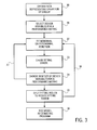
- FIG. 3 is a flow diagram illustrating various steps used in embodiments of the present invention.
- FIG. 4 illustrates two additional steps used in an embodiment of the present invention.
- FIG. 5 is a graph showing several functions and the errors that occur at the transition from one function to another.
- A method for modeling the electrical characteristics of an integrated circuit is described. In the following description, a specific example concerning a CMOS inverter is described. It will be apparent that the present invention may be easily generalized to describe the electrical characteristic of any integrated circuit having transistors or other active or passive devices. Additionally well-known mathematical concepts have not been described in detail in order not to unnecessarily obscure the present invention.
- In FIG. 1 a typical MOS inverter is illustrated. It comprises a
PMOS transistor 10 and anNMOS transistor 11 connected in series with a power supply (Vdd). The common terminal between thetransistors capacitor 13 used to represent output capacitance or load capacitance. The gates of thetransistors - The design variables defining the operation of the inventor of FIG. 1 are: the channel width of
transistors 10 and 11 (Wn and Wp, respectively); the channel length oftransistors 10 and 11 (Ln and Lp, respectively); the number of fingers in the gate oftransistors 10 and 11 (Mn and Mp, respectively); the supply voltage (Vdd); and the load capacitance (Cload). (The number of fingers in the gate refers to the active part of the gate to which the source and drain regions are aligned. This is discussed in the application cited in the prior art section.) - To begin, it is necessary to have data representing the operation of the circuit as shown by
step 30 in FIG. 3. (Generally the log of the data is used as discussed in the prior art) A typical table is illustrated in FIG. 2 with eight design variables and three performance metrics, specifically, peak current, rise time and fall time. Additional performance metrics are possible. Note that there is no unique set of design variables. For example, the transistor active area M W L could have been chosen instead of M. - Data for the design variables and performance metrics can be provided by either actual measurements or from modeling such as with SPICE. Generally, as shown in FIG. 2, the variables, M, W and L are confined to a grid system and only dimensions falling on the grid system are used. Data is obtained over the region necessary for the range of interest. In other words, if T rise must be within 100 ps to 1 ns, only data points that give raise to such values of Trise are entered. Similarly, if it is known that the model will only be used for Cload less than 10 pF, only data that corresponds to Cload less than 10 pF is entered.
- In an integrated circuit, the performance metrics will of course, be a function of the specific process used to fabricate the circuit in addition to the variables, such as shown in FIG. 2. In one embodiment of the present invention, the data which is obtained in
step 30 of FIG. 3, are those variables which are not process dependent. The process dependent variables are used in, for instance, the simulation that occurs with SPICE. This allows the present invention to be implemented in a somewhat process independent manner. From one standpoint, the variables that can be changed are, for example, those as shown in FIG. 2, and typically a circuit designer does not have the opportunity to change the variables in a particular process. - Assume a solution is sought for the performance metrics T rise for the inventor of FIG. 1. A design variable or combination of design variables is selected which highlights or substantially controls the selected operating parameter as shown by
step 31 of FIG. 3. The initial choice of variables is based on some understanding of the behavior of the circuit. - The design variables that are selected can be selected on a trial and error basis, or as stated above, on an understanding of the circuit. By way of example, for the circuit of FIG. 1, if T rise is the performance metric, it is quite apparent that the
capacitor 13 will play a major role in the rise time of the circuit since the capacitor must be charged. Additionally, it is apparent then, that the capacitor is charged throughtransistor 10, and consequently, particularly the width, oftransistor 10 will be significant in the charging of thecapacitor 13. It will also be equally apparent that, for instance, variations in Vdd will not have a major effect on Trise. Similarly, if Tfall is to be considered, again it will be apparent that thecapacitor 13 and the current carrying capacity oftransistor 11 will be critical design variables to consider. - The
next step 32 of FIG. 3 is to model the performance metric as a monomial and/or posynomial function of the design variables or as a max-monomial function. Since the monomial function is, in effect, a subset of posynomial functions the use of the term posynomial also includes monomial for purposes of this application. - One method for fitting mononomial curves known in the prior art is discussed below.
- Assume it is necessary to approximate a function f(x) by a monomial function {circumflex over (f)}(x),where x is a vector of n real positive variables.

- where α 1, α2, . . . , αn∈R and β∈R+ are the function parameters. At first sight, this may seem a complicated nonlinear problem. However, this fitting problem becomes a linear problem with a simple change of variables. First take the logarithm of both sides of equation (3) to obtain, log {circumflex over (f)}(x)=β+α1 log x1+α2log x2+ . . . +αnlog xn.
- Defining α 0=log β, this takes the form of

- which is a linear function of the new parameters y=(α 0, . . . , α4).
- If m sample points of f(x) are used the problem consists in finding a value y such that f≈{circumflex over (f)},

- To find an appropriate value for y, minimize the p-norm of the error.
- minimize∥z−Ay∥p.
- Minimizing the p-norm of the error is a convex problem and can be readily solved. The error distribution depends on the norm chosen. A small p puts more weight on the small errors and a large p puts more weight on the large errors.
- Now described are the details for minimizing the 2-norm and the ∞norm. To minimize 2-norm, solve a least-squares problem, i.e., take y=(A TA)−1ATz, where A is the m×n matrix in the equation (5).
- It is important to realize that this choice of y yields the best fit for log f(x) not for f(x). In other words, minimize ∥log f−log {circumflex over (f)}∥ 2, instead of ∥log f−log {circumflex over (f)}∥2 results. It is interesting to see how these two fitting criteria are related. Minimize,

- For α near 1 log α≈α−1 is obtained. Assuming the fit is good (i.e., (i.e.,({circumflex over (f)} ifi))≈1, one can approximate

- where e i is the square of the percent error for the ith sample. In other words, if the fit is good, the criterion used is quite close to the sum of the squares of the percent errors.
- One can also minimize ∥z−Ay∥∞, i.e.,
- minimize max i|{circumflex over (f)}i−fi|.
- This minimization problem can be written as a linear program, minimize u such that
- log f i−(α0+α1 log x 1i+ . . . +αn log x ni)≦ui=1, . . . m, (6)
- log f i−(α0+α1 log x 1i+ . . . +αn log x ni)≧−ui=1, . . . ,m
- Again, by solving (6), minimizing the maximum error occurs for the fit of log f(x) not for f(x),
- J=maxi|log {circumflex over (f)} i−log f i|=maxi|log {circumflex over (f)} i /f i|.
- By taking the same approximation as before (i.e., for α≈α−1, log α≈α−1), the following can be within,

- If the fit is good, the criterion used is effective to minimize the maximum absolute percent error.
- For a matrix of size 1,000,000×6, the linear problem is solved using MATLAB in approximately forty seconds real time on an ULTRA SPARC1 running at 170 MHz. The computation time scales linearly with the problem size, i.e., problem of size 2,000,000×6, takes around eighty seconds.
- One method for fitting max-monomial curves is the following.
- Assume it is necessary to approximate a function f(x) by a max-monomial function {circumflex over (f)}(x),where x is a vector of n real positive variables. A max-monomial function f(x) is defined as f(x)=max{g i(x)} where gi is a monomial function of x. Thus,

- where α 1,i,α2,i, . . . ,αn,i∈R and β∈R+ are the function parameters. This is equivalent to approximating the function log(f(x)) by a piecewise linear function
- log({circumflex over (f)}(x))=max
— i{log(βi)+α1,i log(x 1)+α2,i log(x 2)+ . . . +αn,i log(x n)} - This method is discussed in detail in “Method for Providing Convex Piecewise-Linear Expression for Multiple Variable System,” application Ser. No. 09/475,734, filed Dec. 30, 1999.
- Assume it is necessary to fit a function f(x) by a posynomial function {circumflex over (f)}(x), where x is a vector of n positive variables. The function posynomial function {circumflex over (f)}(x) has the general form:

- To find a function {circumflex over (f)}(x) posynomial of M monomial terms that describes function f(x), is started with a function {circumflex over (f)} 1(x) posynomial of 1 monomial term and solve the following general nonlinear optimization problem (minimize the p-norm of the error):
- min∥f(x)−{circumflex over (f)}1(x)□p
- This problem can be solved by using readily available nonlinear optimization packages such as ______.
- Now the following optimization problem is solved:
- min∥f(x)−{circumflex over (f)}2(x)∥p
- where {circumflex over (f)} 2(x) is a posynomial of 2 monomial terms. The solution of the problem min∥f(x)−{circumflex over (f)}1(x)∥p is used to compute the starting point of the problem min∥f(x)−{circumflex over (f)}2(x)∥p. Empirically it has been observed that this increases the quality of the fit.
- The above steps are repeated for {circumflex over (f)} 3(x), . . . , {circumflex over (f)}M(x) either until M monomial terms are reached or until the fitting error from {circumflex over (f)}k(x) to {circumflex over (f)}k+1(x) does not improve considerably.
- Once the max-monomial and/or posynomial approximations are found, the fitting error |f(x)−{circumflex over (f)}(x)| is computed. This is shown as
step 33 in FIG. 33. If the error is too large for practical applications steps 32 and 33 are repeated with a different set of design variables until the error is considered acceptable as shown byline 37. IF the error is acceptable , steps 34 and 35 are skipped and the model is used in a geometric program. - If a single max-monomial or posynomial model is not satisfactory, one can create a piecewise max-monomial or posynomial model. To do this, the region of fitting is split. This is done based on some knowledge of the circuit behavior. For example, if no good model can be found for T rise from 100 ps to 1 ns, the desired range of the performance metric can be split into several regions. The split can be based on (1) values of the performance metrics (for example, Trise>500 ps); on (2) values of some of the design variables (for example,

- or on a combination (for example,

- The choice of the “break points” is done through observation and heuristic. For example, assume for the model of T rise:
- Trise={circumflex over (f)}1 for θ≧θ,
- Trise={circumflex over (f)}2 for θ1≦θ≦θ2
- Trise={circumflex over (f)}3 for θ2≦θ≦θ3
- where θ is the splitting parameter and θ 1, and θ2 are the break points.
- Once the performance metric such as T rise is defined in terms of the functions f1,f2 and f3, it may be that at the transitions say between f1 and f2 or f2 and f3 a large amount of error exists. This is shown graphically in FIG. 5. At θ1 (the value of θ selected for transitioning between a first function and a second function) the value for f1 is found as well as the value for f2. As shown in FIG. 5 there may be considerable error between the function f1 at θ, and the function f2 at θ1. If the error (Trise−f1) at θ1 is relatively large compared to the error (Trise−f2) at θ1, moving θ1 in the direction indicated by
arrow 51 in FIG. 5 may minimize the error. Similarly it may occur that by examining error at θ2, the error can be reduced by moving θ2 in the direction indicated byarrow 52. Thus, the data segments can be redivided and if the error is high, say above some predetermined value, then the segments are adjusted so as to minimize the error and new monomial functions are fitted to the new data segments. Sometimes it is required to add new segments. This is shown bysteps - When new segments are obtained new functions are fitted as shown by
line 38. Afterstep 41 is repeated the error is again checked as shown by step 42. If the error is within an acceptable level then steps 35 is skipped. The process of adjusting of the break points for the selected characteristic is repeated until the error is within an acceptable level. Note that for the example above θ is adjusted. - Finally as shown by
step 36 of FIG. 3 the expression representing the performance metric is ready to be used in a geometric program. - Once the posynomial or max-monomial function is found, it then is used in an inequality and solved using geometric programming as taught in the prior art. For instance, once the function for T rise is known, it can be expressed in terms of an inequality to minimize substrate area or power, and then solved with geometric programming. The same would be true, for instance, where a function is developed for an oscillator circuit and an inequality sought to minimize jitter. The resultant solution is used to fabricate an integrated circuit, for instance, having a particular rise time with a minimum of substrate area.
- As mentioned, a max-monomial function f(x) defined as
- {circumflex over (f)}(x)=max{ĝ k(x)} k=1, . . . , p
- where g(x) i are monomials.
- Max-monomial functions can be used in geometric programs as the objective function and/or as constraints.
- Assume a max-monomial is used as the objective in an optimization problem with posynomial inequalities and monomial equalities. The optimization problem would have the following form,
- max {circumflex over (f)}(x)
- f i(x)≦1 =1, , . . . , n
- g j(x)=1 j=1, . . . , m
- x>0
- where {circumflex over (f)}(x) is a max-monomial function as described above, f i(x) are posynomial functions, and gi(x) are monomial functions. This problem can be expressed as,
- max t
- ĝ k(x)≦tk=1, . . . , p
- f i(x)≦1 i=1, . . . , n
- g j(x)=1 j=1, . . . , m
- x<0
- where t is a new design variable. This is equivalent to,
- max f*(x)
- g k*(x)≦1 k=1, . . . , p
- f j(x)<1 i=1, . . . , n
- g j(x)=1 j=1, . . . , m
- x>0
- The problem above fits the general form of a geometric program since f*(x) is a monomial (and therefore posynomial) function and g k*(x)=ĝk(x)/t are monomial (and therefore posynomial) functions. The general form of a geometric program is described in the prior art. Assume now that a max-monomial is used as constraint in an optimization problem with posynomial inequalities, monomial equalities and a posynomial objective. The optimization problem would have the following form,
- max f o(x)
- {circumflex over (f)}(ti x)≦1
- f i(x)≦1=1, , . . . , n
- g j(x)=1 j=1, . . . , m
- x>0
- where {circumflex over (f)}(x) is a max-monomial function as described above, f i(x) are posynomial functions, and gi(x) are monomial functions. This problem can be expressed as,
- max f o(x)
- ĝ k*(x)≦t k=1, . . . , p
- f i(x)≦1 i=1, . . . , n
- g j(x)=1 j=1, . . . , m
- x<0
- where t is a new design variable. This is equivalent to,
- max f o(x)
- g k*(x)≦1 k=1, . . . , p
- f i(x)≦1 i=1, . . . , n
- g j(x)=1 j=1, . . . , m
- x>0
- The problem above fits the general form of a geometric program since

- are monomial (and therefore posynomial) functions. A problem that combines several max-monomial functions in the objective and constraints can also be readily converted into a geometric program by the introduction of additional design variables.
- Thus a method for representing the behavior of an integrated circuit has been disclosed which lends itself to a model that can be used to formulate circuit design problems as geometric programs.
Claims (6)
Priority Applications (3)
| Application Number | Priority Date | Filing Date | Title |
|---|---|---|---|
| US10/118,221 US20030191611A1 (en) | 2002-04-05 | 2002-04-05 | Behavioral circuit modeling for geometric programming |
| AU2003221837A AU2003221837A1 (en) | 2002-04-05 | 2003-04-07 | Behavioral circuit modeling for geometric programming background of the disclosure |
| PCT/US2003/010609 WO2003088097A2 (en) | 2002-04-05 | 2003-04-07 | Behavioral circuit modeling for geometric programming |
Applications Claiming Priority (1)
| Application Number | Priority Date | Filing Date | Title |
|---|---|---|---|
| US10/118,221 US20030191611A1 (en) | 2002-04-05 | 2002-04-05 | Behavioral circuit modeling for geometric programming |
Publications (1)
| Publication Number | Publication Date |
|---|---|
| US20030191611A1 true US20030191611A1 (en) | 2003-10-09 |
Family
ID=28674383
Family Applications (1)
| Application Number | Title | Priority Date | Filing Date |
|---|---|---|---|
| US10/118,221 Abandoned US20030191611A1 (en) | 2002-04-05 | 2002-04-05 | Behavioral circuit modeling for geometric programming |
Country Status (3)
| Country | Link |
|---|---|
| US (1) | US20030191611A1 (en) |
| AU (1) | AU2003221837A1 (en) |
| WO (1) | WO2003088097A2 (en) |
Cited By (2)
| Publication number | Priority date | Publication date | Assignee | Title |
|---|---|---|---|---|
| US20040015787A1 (en) * | 2002-04-10 | 2004-01-22 | Thomas Heydler | Method and apparatus for efficient semiconductor process evaluation |
| US20100299649A1 (en) * | 2004-09-30 | 2010-11-25 | Mar Hershenson | Novel optimization for circuit design |
Citations (31)
| Publication number | Priority date | Publication date | Assignee | Title |
|---|---|---|---|---|
| US4827428A (en) * | 1985-11-15 | 1989-05-02 | American Telephone And Telegraph Company, At&T Bell Laboratories | Transistor sizing system for integrated circuits |
| US5055716A (en) * | 1990-05-15 | 1991-10-08 | Siarc | Basic cell for bicmos gate array |
| US5289021A (en) * | 1990-05-15 | 1994-02-22 | Siarc | Basic cell architecture for mask programmable gate array with 3 or more size transistors |
| US5633807A (en) * | 1995-05-01 | 1997-05-27 | Lucent Technologies Inc. | System and method for generating mask layouts |
| US5654883A (en) * | 1993-06-11 | 1997-08-05 | Canon Kabushiki Kaisha | Power control apparatus and method and power generating system using them |
| US5754826A (en) * | 1995-08-04 | 1998-05-19 | Synopsys, Inc. | CAD and simulation system for targeting IC designs to multiple fabrication processes |
| US5973524A (en) * | 1998-03-25 | 1999-10-26 | Silsym, Inc. | Obtaining accurate on-chip time-constants and conductances |
| US6002860A (en) * | 1996-09-27 | 1999-12-14 | Nortel Networks Corporation | High frequency noise and impedance matched integrated circuits |
| US6209122B1 (en) * | 1995-05-01 | 2001-03-27 | Synopsys, Inc. | Minimization of circuit delay and power through transistor sizing |
| US6253164B1 (en) * | 1997-12-24 | 2001-06-26 | Silicon Graphics, Inc. | Curves and surfaces modeling based on a cloud of points |
| US6269277B1 (en) * | 1998-07-27 | 2001-07-31 | The Leland Stanford Junior University Board Of Trustees | System and method for designing integrated circuits |
| US6295635B1 (en) * | 1998-11-17 | 2001-09-25 | Agilent Technologies, Inc. | Adaptive Multidimensional model for general electrical interconnection structures by optimizing orthogonal expansion parameters |
| US6311145B1 (en) * | 1999-06-17 | 2001-10-30 | The Board Of Trustees Of The Leland Stanford Junior University | Optimal design of an inductor and inductor circuit |
| US6311315B1 (en) * | 1996-09-12 | 2001-10-30 | Matsushita Electric Industrial Co., Ltd. | Semiconductor integrated circuit, design method and computer-readable recording medium |
| US6381563B1 (en) * | 1999-01-22 | 2002-04-30 | Cadence Design Systems, Inc. | System and method for simulating circuits using inline subcircuits |
| US6415417B1 (en) * | 1999-03-01 | 2002-07-02 | Matsushita Electric Industrial Co., Ltd. | Method and apparatus for transistor optimization, method and apparatus for layout design of integrated circuit, and integrated circuit |
| US6425111B1 (en) * | 1999-12-30 | 2002-07-23 | The Board Of Trustees Of The Leland Stanford Junior University | Saturation region transistor modeling for geometric programming |
| US20020184603A1 (en) * | 2001-04-25 | 2002-12-05 | Arash Hassibi | Optimal simultaneous design and floorplanning of integrated circuit |
| US6532569B1 (en) * | 1999-06-18 | 2003-03-11 | Synopsys, Inc. | Classification of the variables in a system of simultaneous equations described by hardware description languages |
| US6539533B1 (en) * | 2000-06-20 | 2003-03-25 | Bae Systems Information And Electronic Systems Integration, Inc. | Tool suite for the rapid development of advanced standard cell libraries |
| US6574786B1 (en) * | 2000-07-21 | 2003-06-03 | Aeroflex UTMC Microelectronics Systems, Inc. | Gate array cell generator using cadence relative object design |
| US6578179B2 (en) * | 2000-09-29 | 2003-06-10 | Kabushiki Kaisha Toshiba | LSI layout design apparatus, layout design method, recording medium recording layout design program, and semiconductor integrated circuit |
| US6577992B1 (en) * | 1999-05-07 | 2003-06-10 | Nassda Corporation | Transistor level circuit simulator using hierarchical data |
| US6581188B1 (en) * | 1999-07-29 | 2003-06-17 | Mitsubishi Denki Kabushiki Kaisha | Semiconductor device and method of designing the same |
| US6588002B1 (en) * | 2001-08-28 | 2003-07-01 | Conexant Systems, Inc. | Method and system for predictive layout generation for inductors with reduced design cycle |
| US20040172609A1 (en) * | 2002-03-05 | 2004-09-02 | Arash Hassibi | Method and apparatus for automatic analog/mixed signal system design using geometric programming |
| US6813590B1 (en) * | 1999-12-30 | 2004-11-02 | Barcelona Design, Inc. | Method for providing convex piecewise-linear expression for multiple variable system |
| US6909330B2 (en) * | 2002-04-07 | 2005-06-21 | Barcelona Design, Inc. | Automatic phase lock loop design using geometric programming |
| US20050251373A1 (en) * | 2001-10-31 | 2005-11-10 | Walter Daems | Posynomial modeling, sizing, optimization and control of physical and non-physical systems |
| US20050273732A1 (en) * | 2004-06-04 | 2005-12-08 | Yang Xu | Optimization and design method for configurable analog circuits and devices |
| US7093205B2 (en) * | 2002-04-10 | 2006-08-15 | Barcelona Design, Inc. | Method and apparatus for efficient semiconductor process evaluation |
-
2002
- 2002-04-05 US US10/118,221 patent/US20030191611A1/en not_active Abandoned
-
2003
- 2003-04-07 AU AU2003221837A patent/AU2003221837A1/en not_active Abandoned
- 2003-04-07 WO PCT/US2003/010609 patent/WO2003088097A2/en not_active Application Discontinuation
Patent Citations (35)
| Publication number | Priority date | Publication date | Assignee | Title |
|---|---|---|---|---|
| US4827428A (en) * | 1985-11-15 | 1989-05-02 | American Telephone And Telegraph Company, At&T Bell Laboratories | Transistor sizing system for integrated circuits |
| US5055716A (en) * | 1990-05-15 | 1991-10-08 | Siarc | Basic cell for bicmos gate array |
| US5055716B1 (en) * | 1990-05-15 | 1992-12-15 | El Gamal Abbas | |
| US5289021A (en) * | 1990-05-15 | 1994-02-22 | Siarc | Basic cell architecture for mask programmable gate array with 3 or more size transistors |
| US5654883A (en) * | 1993-06-11 | 1997-08-05 | Canon Kabushiki Kaisha | Power control apparatus and method and power generating system using them |
| US6209122B1 (en) * | 1995-05-01 | 2001-03-27 | Synopsys, Inc. | Minimization of circuit delay and power through transistor sizing |
| US5633807A (en) * | 1995-05-01 | 1997-05-27 | Lucent Technologies Inc. | System and method for generating mask layouts |
| US5754826A (en) * | 1995-08-04 | 1998-05-19 | Synopsys, Inc. | CAD and simulation system for targeting IC designs to multiple fabrication processes |
| US6311315B1 (en) * | 1996-09-12 | 2001-10-30 | Matsushita Electric Industrial Co., Ltd. | Semiconductor integrated circuit, design method and computer-readable recording medium |
| US6002860A (en) * | 1996-09-27 | 1999-12-14 | Nortel Networks Corporation | High frequency noise and impedance matched integrated circuits |
| US6253164B1 (en) * | 1997-12-24 | 2001-06-26 | Silicon Graphics, Inc. | Curves and surfaces modeling based on a cloud of points |
| US5973524A (en) * | 1998-03-25 | 1999-10-26 | Silsym, Inc. | Obtaining accurate on-chip time-constants and conductances |
| US6269277B1 (en) * | 1998-07-27 | 2001-07-31 | The Leland Stanford Junior University Board Of Trustees | System and method for designing integrated circuits |
| US6295635B1 (en) * | 1998-11-17 | 2001-09-25 | Agilent Technologies, Inc. | Adaptive Multidimensional model for general electrical interconnection structures by optimizing orthogonal expansion parameters |
| US6381563B1 (en) * | 1999-01-22 | 2002-04-30 | Cadence Design Systems, Inc. | System and method for simulating circuits using inline subcircuits |
| US6415417B1 (en) * | 1999-03-01 | 2002-07-02 | Matsushita Electric Industrial Co., Ltd. | Method and apparatus for transistor optimization, method and apparatus for layout design of integrated circuit, and integrated circuit |
| US6577992B1 (en) * | 1999-05-07 | 2003-06-10 | Nassda Corporation | Transistor level circuit simulator using hierarchical data |
| US6311145B1 (en) * | 1999-06-17 | 2001-10-30 | The Board Of Trustees Of The Leland Stanford Junior University | Optimal design of an inductor and inductor circuit |
| US6532569B1 (en) * | 1999-06-18 | 2003-03-11 | Synopsys, Inc. | Classification of the variables in a system of simultaneous equations described by hardware description languages |
| US6581188B1 (en) * | 1999-07-29 | 2003-06-17 | Mitsubishi Denki Kabushiki Kaisha | Semiconductor device and method of designing the same |
| US6425111B1 (en) * | 1999-12-30 | 2002-07-23 | The Board Of Trustees Of The Leland Stanford Junior University | Saturation region transistor modeling for geometric programming |
| US6813590B1 (en) * | 1999-12-30 | 2004-11-02 | Barcelona Design, Inc. | Method for providing convex piecewise-linear expression for multiple variable system |
| US6539533B1 (en) * | 2000-06-20 | 2003-03-25 | Bae Systems Information And Electronic Systems Integration, Inc. | Tool suite for the rapid development of advanced standard cell libraries |
| US6574786B1 (en) * | 2000-07-21 | 2003-06-03 | Aeroflex UTMC Microelectronics Systems, Inc. | Gate array cell generator using cadence relative object design |
| US6578179B2 (en) * | 2000-09-29 | 2003-06-10 | Kabushiki Kaisha Toshiba | LSI layout design apparatus, layout design method, recording medium recording layout design program, and semiconductor integrated circuit |
| US20020184603A1 (en) * | 2001-04-25 | 2002-12-05 | Arash Hassibi | Optimal simultaneous design and floorplanning of integrated circuit |
| US7065727B2 (en) * | 2001-04-25 | 2006-06-20 | Barcelona Design, Inc. | Optimal simultaneous design and floorplanning of integrated circuit |
| US6588002B1 (en) * | 2001-08-28 | 2003-07-01 | Conexant Systems, Inc. | Method and system for predictive layout generation for inductors with reduced design cycle |
| US20050251373A1 (en) * | 2001-10-31 | 2005-11-10 | Walter Daems | Posynomial modeling, sizing, optimization and control of physical and non-physical systems |
| US7162402B2 (en) * | 2001-10-31 | 2007-01-09 | Kimotion Technologies, Inc. | Posynomial modeling, sizing, optimization and control of physical and non-physical systems |
| US20040172609A1 (en) * | 2002-03-05 | 2004-09-02 | Arash Hassibi | Method and apparatus for automatic analog/mixed signal system design using geometric programming |
| US6909330B2 (en) * | 2002-04-07 | 2005-06-21 | Barcelona Design, Inc. | Automatic phase lock loop design using geometric programming |
| US7093205B2 (en) * | 2002-04-10 | 2006-08-15 | Barcelona Design, Inc. | Method and apparatus for efficient semiconductor process evaluation |
| US20050273732A1 (en) * | 2004-06-04 | 2005-12-08 | Yang Xu | Optimization and design method for configurable analog circuits and devices |
| US7350164B2 (en) * | 2004-06-04 | 2008-03-25 | Carnegie Mellon University | Optimization and design method for configurable analog circuits and devices |
Cited By (5)
| Publication number | Priority date | Publication date | Assignee | Title |
|---|---|---|---|---|
| US20040015787A1 (en) * | 2002-04-10 | 2004-01-22 | Thomas Heydler | Method and apparatus for efficient semiconductor process evaluation |
| US7093205B2 (en) | 2002-04-10 | 2006-08-15 | Barcelona Design, Inc. | Method and apparatus for efficient semiconductor process evaluation |
| US20100299649A1 (en) * | 2004-09-30 | 2010-11-25 | Mar Hershenson | Novel optimization for circuit design |
| US8407651B2 (en) * | 2004-09-30 | 2013-03-26 | Synopsys, Inc. | Optimization for circuit design |
| US8635564B2 (en) | 2004-09-30 | 2014-01-21 | Synopsys, Inc. | Parameter optimization for circuit design |
Also Published As
| Publication number | Publication date |
|---|---|
| WO2003088097A3 (en) | 2004-07-08 |
| WO2003088097A2 (en) | 2003-10-23 |
| AU2003221837A1 (en) | 2003-10-27 |
Similar Documents
| Publication | Publication Date | Title |
|---|---|---|
| del Mar Hershenson et al. | GPCAD: A tool for CMOS op-amp synthesis | |
| US6813750B2 (en) | Logic circuit design equipment and method for designing logic circuit for reducing leakage current | |
| US6393601B1 (en) | Layout designing apparatus for integrated circuit, transistor size determining apparatus, circuit characteristic evaluating method, and transistor size determining method | |
| Dhamdhere et al. | How to pay, come what may: Approximation algorithms for demand-robust covering problems | |
| Archibald et al. | On the generation of markov decision processes | |
| US6304836B1 (en) | Worst case design parameter extraction for logic technologies | |
| US8423341B2 (en) | Method and system for constructing corner models for multiple performance targets | |
| US10585136B2 (en) | Method of characterizing and modeling leakage statistics and threshold voltage for ensemble devices | |
| Devonport et al. | Bayesian safe learning and control with sum-of-squares analysis and polynomial kernels | |
| US20030191611A1 (en) | Behavioral circuit modeling for geometric programming | |
| Xia et al. | A discrete-time recurrent neural network for shortest-path routing | |
| Girardi et al. | Power constrained design optimization of analog circuits based on physical gm/ID characteristics | |
| US6691285B1 (en) | Exponential increments in FET size selection | |
| Deyati et al. | An automated design methodology for yield aware analog circuit synthesis in submicron technology | |
| Lima et al. | Tsallis statistics with normalized q-expectation values is thermodynamically stable: illustrations | |
| Yu et al. | Parametric yield optimization of CMOS analogue circuits by quadratic statistical circuit performance models | |
| Girardi et al. | A tool for automatic design of analog circuits based on gm/i/sub d/methodology | |
| US6629301B1 (en) | Determining transistor widths using the theory of logical effort | |
| US7117128B2 (en) | Method and apparatus for digital signal filtering | |
| Proschan | The normal approximation to the binomial | |
| Moriarty et al. | The Skipping Sampler: A new approach to sample from complex conditional densities | |
| Zheng et al. | iVAMS: Intelligent metamodel-integrated Verilog-AMS for circuit-accurate system-level mixed-signal design exploration | |
| Kundu et al. | An efficient method of Pareto-optimal front generation for analog circuits | |
| US8375341B2 (en) | Method for improving the radio frequency linearity of silicon-on-insulator MOSFET circuits | |
| Adamski | Multi-Objective Differentiable Neural Architecture Search Busca Multiobjetivo e Diferenciável de Arquitetura de Rede Neural |
Legal Events
| Date | Code | Title | Description |
|---|---|---|---|
| AS | Assignment |
Owner name: BARCELONA DESIGN, INC., CALIFORNIA Free format text: ASSIGNMENT OF ASSIGNORS INTEREST;ASSIGNORS:HERSHENSON, MARIA DEL MAR;COLLERAN, DAVE;HASSIBI, ARASH;REEL/FRAME:013039/0808;SIGNING DATES FROM 20020604 TO 20020613 |
|
| AS | Assignment |
Owner name: SABIO LABS, INC., CALIFORNIA Free format text: ASSIGNMENT OF ASSIGNORS INTEREST;ASSIGNOR:BARCELONA DESIGN, INC.;REEL/FRAME:019062/0574 Effective date: 20070309 |
|
| AS | Assignment |
Owner name: SABIO LABS, INC., CALIFORNIA Free format text: ASSIGNMENT OF ASSIGNORS INTEREST;ASSIGNOR:BARCELONA DESIGN, INC.;REEL/FRAME:019278/0549 Effective date: 20070309 |
|
| AS | Assignment |
Owner name: MAGMA DESIGN AUTOMATION, INC., CALIFORNIA Free format text: MERGER;ASSIGNOR:SABIO LABS, INC.;REEL/FRAME:021658/0535 Effective date: 20071220 |
|
| AS | Assignment |
Owner name: WELLS FARGO CAPITAL FINANCE, LLC,CALIFORNIA Free format text: SECURITY AGREEMENT;ASSIGNOR:MAGMA DESIGN AUTOMATION, INC.;REEL/FRAME:024120/0809 Effective date: 20100319 Owner name: WELLS FARGO CAPITAL FINANCE, LLC, CALIFORNIA Free format text: SECURITY AGREEMENT;ASSIGNOR:MAGMA DESIGN AUTOMATION, INC.;REEL/FRAME:024120/0809 Effective date: 20100319 |
|
| STCB | Information on status: application discontinuation |
Free format text: ABANDONED -- FAILURE TO RESPOND TO AN OFFICE ACTION |
|
| AS | Assignment |
Owner name: SYNOPSYS, INC., CALIFORNIA Free format text: RELEASE BY SECURED PARTY;ASSIGNOR:WELLS FARGO CAPITAL FINANCE, LLC;REEL/FRAME:040607/0632 Effective date: 20161031 |