US20030190112A1 - NxN switching arrangement of two planar arrays without waveguide crossings - Google Patents
NxN switching arrangement of two planar arrays without waveguide crossings Download PDFInfo
- Publication number
- US20030190112A1 US20030190112A1 US10/115,828 US11582802A US2003190112A1 US 20030190112 A1 US20030190112 A1 US 20030190112A1 US 11582802 A US11582802 A US 11582802A US 2003190112 A1 US2003190112 A1 US 2003190112A1
- Authority
- US
- United States
- Prior art keywords
- array
- optical
- imaging
- interconnection arrangement
- optical interconnection
- Prior art date
- Legal status (The legal status is an assumption and is not a legal conclusion. Google has not performed a legal analysis and makes no representation as to the accuracy of the status listed.)
- Granted
Links
Images


Classifications
-
- G—PHYSICS
- G02—OPTICS
- G02B—OPTICAL ELEMENTS, SYSTEMS OR APPARATUS
- G02B6/00—Light guides; Structural details of arrangements comprising light guides and other optical elements, e.g. couplings
- G02B6/24—Coupling light guides
- G02B6/26—Optical coupling means
- G02B6/32—Optical coupling means having lens focusing means positioned between opposed fibre ends
-
- G—PHYSICS
- G02—OPTICS
- G02B—OPTICAL ELEMENTS, SYSTEMS OR APPARATUS
- G02B6/00—Light guides; Structural details of arrangements comprising light guides and other optical elements, e.g. couplings
- G02B6/24—Coupling light guides
- G02B6/26—Optical coupling means
- G02B6/35—Optical coupling means having switching means
- G02B6/354—Switching arrangements, i.e. number of input/output ports and interconnection types
- G02B6/3544—2D constellations, i.e. with switching elements and switched beams located in a plane
- G02B6/3546—NxM switch, i.e. a regular array of switches elements of matrix type constellation
-
- G—PHYSICS
- G02—OPTICS
- G02B—OPTICAL ELEMENTS, SYSTEMS OR APPARATUS
- G02B6/00—Light guides; Structural details of arrangements comprising light guides and other optical elements, e.g. couplings
- G02B6/24—Coupling light guides
- G02B6/26—Optical coupling means
- G02B6/35—Optical coupling means having switching means
- G02B6/354—Switching arrangements, i.e. number of input/output ports and interconnection types
- G02B6/356—Switching arrangements, i.e. number of input/output ports and interconnection types in an optical cross-connect device, e.g. routing and switching aspects of interconnecting different paths propagating different wavelengths to (re)configure the various input and output links
Definitions
- This invention relates to N ⁇ N optical crossconnect switches, and more particularly, to an N ⁇ N crossconnect switching arrangement of two planar arrays without waveguide crossings.
- N ⁇ N crossconnect switch In high capacity optical networks, an essential device is the N ⁇ N crossconnect switch.
- the function of this device is to provide at each node full connectivity among several incoming fibers, each carrying several wavelength channels.
- the switch must be nonblocking, and it must be fast and efficient [1-3].
- These properties can be realized with minimal depth 2log N and low crosstalk by using a crossbar arrangement of binary trees, consisting of 2N(N ⁇ 1)1 ⁇ 2 and 2 ⁇ 1 elements [1-3]. This approach, however, is difficult to realize in integrated form on a single wafer, because of its large number of waveguide crossings.
- N ⁇ N crossconnect switch that can be implemented without the use of waveguide crossings. Since it is free of waveguide crossings, and it is essentially equivalent to the classical crossbar arrangement, it may be superior to previous arrangements based on integrated optics.
- our N ⁇ N crossconnect switch uses two separate imaging arrangements consisting of two planar arrays of 1 ⁇ 2 and 2 ⁇ 1 switching elements combined with a cylindrical reflector.
- the N ⁇ N crossconnect switch includes an input planar array and output planar array implemented on a single wafer both having a refractive index n separated by a central region having a refractive index n 0 ⁇ n.
- our N ⁇ N optical interconnection arrangement comprises
- the first array including N imaging elements, each imaging element having N input waveguides coupled thereto,
- the second array including N imaging elements, each imaging element having N output waveguides coupled thereto and wherein
- each input waveguide of a particular imaging element of the first array is coupled to a unique output waveguide of a corresponding imaging element of the second array.
- the N ⁇ N optical interconnection arrangement may be implemented using input and output arrays formed on a single wafer or by using input and output arrays formed on separate wafers coupled together with a cylindrical reflector.
- An N ⁇ N optical switch is formed by adding a 1 ⁇ N switch array to each transmitting element and an N ⁇ 1 switch array connected to each receiving element of the N ⁇ N optical interconnection arrangement.
- FIG. 1 illustrates an imaging arrangement of two periodic slabs.
- FIG. 2 shows an array element combined with an input 1 ⁇ N switch.
- FIG. 3 shows that each transmitting (or receiving) array element can be characterized by a perfect focal point F.
- FIG. 4 shows the imaging between two particular array elements.
- FIG. 5 shows the imaging conditions that must be satisfied between two conjugate tapers.
- FIG. 6 shows a confocal arrangement
- FIG. 7 shows two planar wafers combined with a circular cylinder reflector.
- FIG. 8 shows a planar wafer with a nearly periodic profile formed by etching.
- FIG. 9 shows a planar wafer formed to produce a straight focal line.
- FIG. 9A shows a cross-section, a-a′, of FIG. 9 as viewed in the X-direction.
- the classical N ⁇ N crossconnect switch arrangement consists of a 1 ⁇ N switch array and an N ⁇ 1 switch array, which requires a total of N 2 connections, between the various switches.
- the N 2 connections make the arrangement difficult to realize in integrated form for large N on a single wafer, because of the large number of waveguide crossings required by the various connections.
- a planar imaging arrangement of two arrays combined with a cylindrical reflector We first describe an equivalent arrangement without cylindrical reflector. Thus, we initially assume a planar free-space between the two arrays. The following configuration is closely related to the confocal arrangement used in [4].
- any crossbar switching arrangement for instance including wavelength routers instead of ordinary 1 ⁇ N and N ⁇ 1 switches.
- switching arrangements can be constructed, for instance by using ordinary 1 ⁇ N and N ⁇ 1 switches for both arrays, a 1 ⁇ N switch for the first array and wavelength routers for the second array, wavelength routers for the first array and N ⁇ 1 switches for the second array, or using wavelength grating routers for both arrays.
- the 1 ⁇ N and N ⁇ 1 switch arrangements may be implemented as described in pending U.S. patent application Ser. No. 09/687,346, filed on Oct.
- the wavelength routers may be implemented as described in U.S. Pat. No. 5,136,671, issued on Aug. 4, 1992 and entitled “OPTICAL SWITCH, MULTIPLEXER, AND DEMULTIPLEXER.”
- each transmitting element of array 101 can efficiently transmit to any one of the N receiving elements of array 102 , and each receiving element can efficiently receive from any of the N transmitting elements.
- each transmitting element of array 101 connects to an output port of the 1 ⁇ N switch and a similar arrangement is used for the receiving array 102 (not shown) but which is simply the mirror image of the transmitting array 101 .
- Each imaging element in FIG. 2 connects to one of the N waveguides of the 1 ⁇ N switch, which are located close to the focal curve of the refractive edge L of array 101 . Similar considerations apply to each receiving element of array 102 , which again consists of refractive curve L connected to N receiving waveguides, which are now connected to a N ⁇ 1 switch.
- each array 101 and 102 includes N elements.
- each array is characterized by N focal points, and efficient transmission between the elements of the two arrays is realized by simply placing in the vicinity of each focal point N waveguides.
- the resulting arrangement is then capable of providing N 2 connections.
- Each optical connection is formed as shown schematically in FIG.
- FIGS. 1, 3, 4 only show a schematic representation of imaging according to geometric optics.
- the actual rays in practice are curved, because of diffraction, as shown for instance in FIG. 6, as is well known from the laws of Gaussian Optics.
- each waveguide is actually displaced from the focal curve of the imaging element. The displacement is typically small, and it varies depending on the particular design. Its optimum value is obtained in each case by maximizing the transmission coefficient from a particular input waveguide to the corresponding output waveguide. As disclosed later two different optimizations are obtained, depending on whether or not a wide wavelength range of efficient performance is specified.
- FIG. 5 shows the connection between two waveguides 501 and 502 , as in FIG. 4, except that in FIG. 5 the waveguides include tapers 503 504 at the junctions with the free-space regions 520 , 521 . Notice the tapered section of each waveguide has its aperture centered at F 0 .
- the purpose of the taper is to produce over its aperture a curved wavefront centered at A 0 , which will be referred to as the phase center of the taper.
- a 0 which will be referred to as the phase center of the taper.
- the latter condition is needed to insure the phase match, and it requires suitable tapers 503 , 504 as shown in FIG. 5.
- the purpose of the input taper 503 in FIG. 5 is to illuminate the waveguide aperture with a curved phase front centered at the apex A 0 of the taper.
- ⁇ , R are determined by the distance R 0 between the two arrays and the lateral displacement of the two elements.
- FIG. 4 illustratively shows R and R 0 for two elements that are laterally displaced.
- W is the total element aperture width, which is typically somewhat greater than the aperture illumination width w considered earlier.
- FIG. 6 This requirement, which was satisfied by the FIG. 5 imaging arrangement, can now be satisfied in many different ways.
- One way uses a confocal arrangement shown in FIG. 6.
- the input curve 601 we specify the input curve 601 to be a straight line and one can show that the optimum arrangement for our purpose here is then obtained by choosing the beam radius w 1 on the two refracting curves so that approximately ⁇ 0 ⁇ R ⁇ ⁇ ⁇ w 1 2 ⁇ 1 ,
- R is appreciably larger than the focal length r of the two refractive curves, and ⁇ ⁇ ⁇ w 0 2 ⁇ 0 ⁇ r 0 ⁇ ⁇ 1
- w 0 is the beam radius over the waveguide 602 aperture.
- the first refractive curve 603 is accurately illuminated by the Fourier transform of the input mode and, the other curve 604 , by a magnified image of the input mode. Therefore, a perfect match between the two waveguides 601 , 605 is not possible. This would strictly require, in view of the arrangement symmetry, the two illuminations to be identical at all wavelengths. Instead, the width of the first illumination is a linear function of the wavelength ⁇ , whereas the second width is wavelength independent, and therefore the two widths can only be matched in the vicinity of a particular wavelength ⁇ 0 . In spite of this disadvantage, as compared to the previous imaging arrangement, the confocal arrangement is generally preferable, because it minimizes the beam radius w 1 on the refractive surface.
- the medium in the region 103 of FIG. 1 is ordinary free-space and combine the two arrays with a cylindrical lens, or equivalently a reflector as shown in FIG. 7.
- Shown in FIG. 7 is a cylindrical reflector 706 , and two wafers 701 and 702 , each including identical imaging arrays 703 , 704 and their associated switches or routers.
- the reflector 706 is characterized by two focal lines, such that a cylindrical wave originating from either line is transformed after reflection into a cylindrical wave converging towards the second line.
- the transmitting array 703 must be implemented to now behave as a line source, and similarly the receiving array 704 , must have the conjugate (mirror image) behavior.
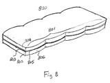
- FIG. 8 Shown in FIG. 8 is an illustrative transmitting array 800 with a cylindrical surface with approximately periodic element profile 801 which is shown as a slab which includes a lower cladding region 802 , a core region 803 and an upper cladding region 804 . Notice the curved edge 805 of the core in FIG. 8 is shown for simplicity on the curved cylindrical surface 806 of the wafer. In practice the core edge must be displaced from the cylindrical surface for the following reason. In FIG.
- an optical signal traveling in the core region 803 between the lower 802 and upper 803 cladding regions would produce, after diffraction by the cylindrical surface, a diffracted wave essentially emanating from the edge 805 of core region 803 .
- What is desired here is to produce a straight-line source rather than a curved line source. Therefore, in order to produce a straight-line source, the curved edge of the core region must be modified as shown in FIG. 9. In FIG.
- FIG. 9A Shown in FIG. 9A is a cross-section (a-a′) of FIG.
- the above arrangement is essentially free of aberrations.
- An estimate of its dimensions can be made as follows.
- the width W of each element is primarily determined by the width of each 1 ⁇ N and N ⁇ 1 switch, and it can be expressed as
- the average spacing S can be about 50 microns.
- Efficient power transfer between two identical waveguides requires in general the aperture distribution of either waveguide to be a replica of the other.
- the imaging arrangement of FIG. 5 is attractive because it is very efficient over a very wide range of wavelengths, but it requires tapered waveguides, in order to insure that the phase distribution over either aperture is the mirror image of the other. It turns out that the phase errors produced in the above imaging arrangement without tapers are typically small.
- the confocal arrangement is preferable, in general, since it does not require tapers and it minimizes the illumination width on each refractive curve. Then, however, the two aperture distributions are related by a Fourier transformation, which causes a small mismatch between the two distributions.
Abstract
Description
- This invention relates to N×N optical crossconnect switches, and more particularly, to an N×N crossconnect switching arrangement of two planar arrays without waveguide crossings.
- In high capacity optical networks, an essential device is the N×N crossconnect switch. The function of this device is to provide at each node full connectivity among several incoming fibers, each carrying several wavelength channels. The switch must be nonblocking, and it must be fast and efficient [1-3]. These properties can be realized with minimal depth 2log N and low crosstalk by using a crossbar arrangement of binary trees, consisting of 2N(N−1)1×2 and 2×1 elements [1-3]. This approach, however, is difficult to realize in integrated form on a single wafer, because of its large number of waveguide crossings.
- What is needed is an N×N crossconnect switch, which can be implemented without the use of waveguide crossings.
- In accordance with the present invention, we describe an N×N crossconnect switch that can be implemented without the use of waveguide crossings. Since it is free of waveguide crossings, and it is essentially equivalent to the classical crossbar arrangement, it may be superior to previous arrangements based on integrated optics. In one embodiment, our N×N crossconnect switch uses two separate imaging arrangements consisting of two planar arrays of 1×2 and 2×1 switching elements combined with a cylindrical reflector. In another embodiment, the N×N crossconnect switch includes an input planar array and output planar array implemented on a single wafer both having a refractive index n separated by a central region having a refractive index n 0<n.
- More generally, our N×N optical interconnection arrangement comprises
- a first and second planar array,
- the first array including N imaging elements, each imaging element having N input waveguides coupled thereto,
- the second array including N imaging elements, each imaging element having N output waveguides coupled thereto and wherein
- each input waveguide of a particular imaging element of the first array is coupled to a unique output waveguide of a corresponding imaging element of the second array.
- The N×N optical interconnection arrangement may be implemented using input and output arrays formed on a single wafer or by using input and output arrays formed on separate wafers coupled together with a cylindrical reflector. An N×N optical switch is formed by adding a 1×N switch array to each transmitting element and an N×1 switch array connected to each receiving element of the N×N optical interconnection arrangement.
- In the drawings,
- FIG. 1 illustrates an imaging arrangement of two periodic slabs.
- FIG. 2 shows an array element combined with an input 1×N switch.
- FIG. 3 shows that each transmitting (or receiving) array element can be characterized by a perfect focal point F.
- FIG. 4 shows the imaging between two particular array elements.
- FIG. 5 shows the imaging conditions that must be satisfied between two conjugate tapers.
- FIG. 6 shows a confocal arrangement.
- FIG. 7 shows two planar wafers combined with a circular cylinder reflector.
- FIG. 8 shows a planar wafer with a nearly periodic profile formed by etching.
- FIG. 9 shows a planar wafer formed to produce a straight focal line.
- FIG. 9A shows a cross-section, a-a′, of FIG. 9 as viewed in the X-direction.
- In the following description, identical element designations in different figures represent identical elements. Additionally in each element designation, the first digit refers to the figure in which that element is first located (e.g., 104 is first located in FIG. 1).
- 1. Imaging Arrangement of Two Arrays of Binary Trees
- The classical N×N crossconnect switch arrangement consists of a 1×N switch array and an N×1 switch array, which requires a total of N 2 connections, between the various switches. The N2 connections make the arrangement difficult to realize in integrated form for large N on a single wafer, because of the large number of waveguide crossings required by the various connections. In the present application we propose, as a remedy to this problem, a planar imaging arrangement of two arrays combined with a cylindrical reflector. We first describe an equivalent arrangement without cylindrical reflector. Thus, we initially assume a planar free-space between the two arrays. The following configuration is closely related to the confocal arrangement used in [4]. Here we consider an arrangement of switches, but the following considerations also apply to any crossbar switching arrangement, for instance including wavelength routers instead of ordinary 1×N and N×1 switches. Thus a variety of such switching arrangements can be constructed, for instance by using ordinary 1×N and N×1 switches for both arrays, a 1×N switch for the first array and wavelength routers for the second array, wavelength routers for the first array and N×1 switches for the second array, or using wavelength grating routers for both arrays. The 1×N and N×1 switch arrangements may be implemented as described in pending U.S. patent application Ser. No. 09/687,346, filed on Oct. 13, 2000 and entitled “LARGE N×N OPTICAL SWITCH USING BINARY TREES.” The wavelength routers may be implemented as described in U.S. Pat. No. 5,136,671, issued on Aug. 4, 1992 and entitled “OPTICAL SWITCH, MULTIPLEXER, AND DEMULTIPLEXER.”
- We first consider a symmetric arrangement of two identical arrays of
imaging elements central region 103 between the two arrays, and index n>n0 in the regions occupied by the imaging elements. Imaging (from source S to destination Q) by each array element is simply performed by the curved edge separating each array from the central region. The edge is made up of N sections, and each section is combined with a 1×N switch as shown in FIG. 2. Here we assume propagation from left to right but the arrangement is bi-directional. The purpose of the arrangement of FIG. 1 is to transmit each input signal, e.g. S, applied to aparticular element 104 of the transmittingarray 101, to a point Q of aparticular receiving element 105 of theother array 102. Each transmitting element ofarray 101 can efficiently transmit to any one of the N receiving elements ofarray 102, and each receiving element can efficiently receive from any of the N transmitting elements. As shown in FIG. 2, each transmitting element ofarray 101 connects to an output port of the 1×N switch and a similar arrangement is used for the receiving array 102 (not shown) but which is simply the mirror image of the transmittingarray 101. Each imaging element in FIG. 2 connects to one of the N waveguides of the 1×N switch, which are located close to the focal curve of the refractive edge L ofarray 101. Similar considerations apply to each receiving element ofarray 102, which again consists of refractive curve L connected to N receiving waveguides, which are now connected to a N×1 switch. - With reference to FIG. 3, we describe the optimization of the imaging arrangement of FIG. 1. Each
array parallel rays 301, directed towards the central element of the receivingarray 102. As a result, each array is characterized by N focal points, and efficient transmission between the elements of the two arrays is realized by simply placing in the vicinity of each focal point N waveguides. The resulting arrangement is then capable of providing N2 connections. Each optical connection is formed as shown schematically in FIG. 4, by an imaging arrangement of two refractingcurves 401, 402 combined with twowaveguides - Notice FIGS. 1, 3, 4 only show a schematic representation of imaging according to geometric optics. The actual rays in practice are curved, because of diffraction, as shown for instance in FIG. 6, as is well known from the laws of Gaussian Optics. Also notice that each waveguide is actually displaced from the focal curve of the imaging element. The displacement is typically small, and it varies depending on the particular design. Its optimum value is obtained in each case by maximizing the transmission coefficient from a particular input waveguide to the corresponding output waveguide. As disclosed later two different optimizations are obtained, depending on whether or not a wide wavelength range of efficient performance is specified.
- 1.1 Imaging by a Refractive Curve.
- With reference to FIG. 2, consider a particular transmitting element, and let it's refracting edge be illuminated by a point source S. Let r be the focal length f and α, γ be the angles of incidence and refraction for the principal ray through the center C of the refracting edge L. In order to obtain parallel rays after refraction, the edge profile z=z 0(x) must satisfy the condition p=0, where p is the aberration function
- p=p 1 −p 2 =n({square root}{square root over ((x+r sin α)2+(z 0(x)+r 0 cos α)2)}−r)−( x sin γ+z0(x)cos γ), (1)
- assuming refractive index n before refraction, and unity index after refraction. Notice the first term is contributed by the optical path p 1 from S to the refractive edge and, the second term p2 is contributed by the optical path from the refractive edge to a plane orthogonal to the direction specified by γ. Here we specify the above condition for some particular values r0, α0, γ0 of r, α, γ satisfying
- n sin α0=sin γ0, (2)
- and obtain for z=z 0(x) an ellipse with one of its two foci coincident with F. The resulting aberrations p for γ0≠γ can be determined accurately from the expression (1), and they can be minimized by properly choosing r, α for each γ of interest, corresponding to a particular connection with the receiving array. By expanding p in powers of x we eliminate terms of order two by choosing
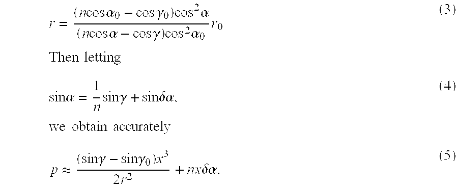
- and determine the optimum δα that minimizes the maximum aberration p max over the diffracting edge aperture. For an aperture width w we obtain

- Notice that aberrations must be minimized over the entire field of view corresponding to the γ—interval occupied by the receiving array. Therefore the optimum γ 0 in the above expression is simply the value corresponding to the center of the receiving array. Then, according to the above expression, all array elements are essentially characterized by the same aberrations.
- 1.2 Optimum Arrangements
- We now derive the conditions that must be satisfied in order to match each input waveguide to the corresponding output waveguide. We initially consider for simplicity the particular case γ=0, but the following considerations apply in general. The following description makes reference to FIG. 5 and considers a particular connection formed between two
particular waveguides waveguides tapers 503 504 at the junctions with the free-space regions input waveguide 501 to be accurately reproduced over the receivingwaveguide 502 aperture. Both amplitude and phase must be matched and, ideally, the match should be wavelength independent. This strictly requires the input mode and its corresponding replica to be produced on conjugate curves satisfying two conditions. First the axial points F0, F of the two curves must be conjugate points (either point must be the image of the other). Second, the centers of curvatures A0,A of the two curves must also be conjugate points. The former condition is needed to guarantee the amplitude match, and it is realized by placing each curve through the focal point of the refracting curve, as shown by 510 for γ=0 in FIG. 5. The latter condition is needed to insure the phase match, and it requiressuitable tapers - The purpose of the
input taper 503 in FIG. 5 is to illuminate the waveguide aperture with a curved phase front centered at the apex A0 of the taper. Theoutput taper 504 is simply the mirror image of the input taper and, in order to produce over its receiving aperture the appropriate phase distribution, its apex A must be the image of A0. Therefore, from the lens equation, the taper length d=A0F0=AF must satisfy
- where R is the distance between the two array elements, and r is the focal length of expression (3). Notice d is the radius of curvature of the phase fronts at F 0, F.
- The values of γ, R are determined by the distance R 0 between the two arrays and the lateral displacement of the two elements. FIG. 4 illustratively shows R and R0 for two elements that are laterally displaced. For a lateral displacement by i elements,

- where W is the total element aperture width, which is typically somewhat greater than the aperture illumination width w considered earlier.
- From expression (6) one can determine the maximum field of view width Ω, obtained by specifying less then λ/4 maximum error. For instance, by using silica waveguides with aperture width of 15 μm and r=4000 μm, one obtains Ω=1.75 for λ=1.55 μm.
- The above conditions are required to insure a good match over a very wide wavelength range. In most cases, however, a good match is only required in the vicinity of a particular wavelength λ=λ 0. Then the design can be simplified and, in particular, the above tapers (503, 504 shown in FIG. 5) are not needed. In fact, a perfect match at a particular wavelength only requires a constant phase distribution on the symmetry axis of the arrangement. This condition, which is a general property of any symmetric arrangement, can be satisfied accurately by approximating the input mode with a Gaussian distribution. Then the above condition simply requires the resulting beam waist between the two refractive curves to be exactly produced in the middle, on the symmetry axis. This requirement, which was satisfied by the FIG. 5 imaging arrangement, can now be satisfied in many different ways. One way uses a confocal arrangement shown in FIG. 6. In the FIG. 6 arrangement, we specify the
input curve 601 to be a straight line and one can show that the optimum arrangement for our purpose here is then obtained by choosing the beam radius w1 on the two refracting curves so that approximately
- which can be shown to minimize w 1 for a given R. Typically, R is appreciably larger than the focal length r of the two refractive curves, and

- where w 0 is the beam radius over the
waveguide 602 aperture. Under the above conditions, the firstrefractive curve 603 is accurately illuminated by the Fourier transform of the input mode and, theother curve 604, by a magnified image of the input mode. Therefore, a perfect match between the twowaveguides - 2. Imaging Arrangement of Two Arrays and a Cylindrical Reflector
- We now assume that the medium in the
region 103 of FIG. 1 is ordinary free-space and combine the two arrays with a cylindrical lens, or equivalently a reflector as shown in FIG. 7. Shown in FIG. 7 is acylindrical reflector 706, and twowafers identical imaging arrays 703, 704 and their associated switches or routers. We assume that thereflector 706 is characterized by two focal lines, such that a cylindrical wave originating from either line is transformed after reflection into a cylindrical wave converging towards the second line. To implement the FIG. 7 arrangement, the transmitting array 703 must be implemented to now behave as a line source, and similarly the receivingarray 704, must have the conjugate (mirror image) behavior. We can realize the curved profile of expression (3) by precision etching a cylindrical surface with approximately periodic profile as shown in FIG. 8 for the transmitting 703 and receiving 704 arrays. Shown in FIG. 8 is anillustrative transmitting array 800 with a cylindrical surface with approximatelyperiodic element profile 801 which is shown as a slab which includes alower cladding region 802, acore region 803 and anupper cladding region 804. Notice thecurved edge 805 of the core in FIG. 8 is shown for simplicity on the curvedcylindrical surface 806 of the wafer. In practice the core edge must be displaced from the cylindrical surface for the following reason. In FIG. 8, an optical signal traveling in thecore region 803 between the lower 802 and upper 803 cladding regions would produce, after diffraction by the cylindrical surface, a diffracted wave essentially emanating from theedge 805 ofcore region 803. In this case, since radiation from thecore region 803 would emanate from thecurved edge 805 of each of thearray elements 801, this would cause each element to effectively behave as a curved line source, formed by thecurved edge 805 of thecore region 803 of the slab. What is desired here is to produce a straight-line source rather than a curved line source. Therefore, in order to produce a straight-line source, the curved edge of the core region must be modified as shown in FIG. 9. In FIG. 9, to better illustrate the modification to thecore region 803 theupper cladding region 804 of the slab 800 (which has the same shape as the lower cladding region 802) is not shown. By properly choosing theedge profile 901 of the core region, we cause its virtual image produced by thecylindrical surface 806 to become astraight line 902. This simply requires theedge profile 901 to be z1−(z0(x)−z1)/n, where z0(x) denotes thecylindrical lens profile 805 specified by the expression (1) for p=0 and z1 is the (negative) coordinate of the focal line. Shown in FIG. 9A is a cross-section (a-a′) of FIG. 9 (as viewed in the X-direction) and avirtual image 902 formed by the diffracted rays emanating from theedge 901 of thecore 803. Notice the cylindrical profile z0(x), 805, must have good optical quality, but it need not be exactly orthogonal to the plane X, Z of the wafer. After deposition of thelower cladding 802, thecore region 803 is deposited and etched to theprofile 901. Then, theupper cladding 805 is deposited and thereafter theprofile 805 is etched vertically, in direction Y, down the face of the slab (through theupper cladding 804,core region 803, and lower cladding 802). During this process however, precise alignment is not required, and errors as large as a few microns can be tolerated. - Once two arrays characterized by straight focal lines are realized, perfect imaging between the two focal lines is obtained by simply using an elliptical cylinder with its focal lines coincident with those of the two arrays. The complete arrangement is illustrated in FIG. 7. The
angle 710 between the twoarrays 703 and 704 is typically very small, and therefore acircular reflector 706 can be used with negligible aberrations. - The above arrangement is essentially free of aberrations. An estimate of its dimensions can be made as follows. The width W of each element is primarily determined by the width of each 1×N and N×1 switch, and it can be expressed as
- w=NS
- where the average spacing S can be about 50 microns. The total width for each array is W=N 2S cm, and the distance R0/2 of the two arrays from the cylindrical reflector of FIG. 10

- for Ω=0.175. For instance, for N=32,

- 3. Concluding Remarks
- To conclude, it is possible to realize large N×N optical crossconnect switches by using a planar arrangement of 1×N and N×1 switches (or routers) combined with 2N imaging elements. The imaging elements are not simple to realize but, in spite of this, the arrangement is attractive because of its expected good performance, since it is equivalent to the classical crossbar arrangement, and it is free of waveguide crossings. For small N, the arrangement can be realized on a single wafer by using two arrays of waveguide lenses (FIG. 1), instead of using a cylindrical reflector arrangement (FIG. 7). However, our derivation of the optimum matching conditions applies to both cases.
- Efficient power transfer between two identical waveguides requires in general the aperture distribution of either waveguide to be a replica of the other. To this purpose, one can either use the imaging arrangement of FIG. 5 or the confocal arrangement [4] as in FIG. 6. The imaging arrangement of FIG. 5 is attractive because it is very efficient over a very wide range of wavelengths, but it requires tapered waveguides, in order to insure that the phase distribution over either aperture is the mirror image of the other. It turns out that the phase errors produced in the above imaging arrangement without tapers are typically small. Nevertheless, the confocal arrangement is preferable, in general, since it does not require tapers and it minimizes the illumination width on each refractive curve. Then, however, the two aperture distributions are related by a Fourier transformation, which causes a small mismatch between the two distributions.
- Finally, an important consideration of 1×N and N×1 switches, which use thermoptic switches, is the total power dissipation. For the classical crossbar 1×N and N×1 switch arrangement, either array requires (N−1)1×2 switching elements but only N log 2 N of these need be turned on at any given time. Therefore assuming for instance 0.4 watts per switch, a total of 25.6 watts would be required for a 16×16 switch.
- [1] Alfemess, R. C., “Guided-wave Devices for Optical Communications,” IEEE J. Quantum Electron., Vol. QE-17, pp. 946-957, 1981.
- [2] Padmanabhan, K., and Netravali, A., “Dilated Networks for Photonic Switching,” IEEE Transactions on Communications, Vol. COM-35, No. 12, pp. 1357-1365, December 1987.
- [3] Dragone, C., “Optimum Nonblocking Networks for Photonic Switching”, invited paper, Millennium Issue of the IEEE Journal of Selected Topics in Quantum Electronics.
- [4] Doerr, C., R., and Dragone, C., “Proposed Optical Crossconnect Using a Planar Arrangement of Beam Steerers”, IEEE Photon. Technol. Lett., Vol.11, No.2, pp.197-109, February 1999.
- [5] Goh, T., Himeno, A., Okuno, M., Takahashi, H., and Hattori, K., “High-Extinction Ratio and Low Loss Silica-Based 8×8 Thermooptic Matrix Switch,” IEEE Photon. Technol. Lett., Vol. 10, No. 3, pp. 358-360, March 1998.
Claims (11)
Priority Applications (1)
| Application Number | Priority Date | Filing Date | Title |
|---|---|---|---|
| US10/115,828 US6859574B2 (en) | 2002-04-03 | 2002-04-03 | N×N switching arrangement of two planar arrays without waveguide crossings |
Applications Claiming Priority (1)
| Application Number | Priority Date | Filing Date | Title |
|---|---|---|---|
| US10/115,828 US6859574B2 (en) | 2002-04-03 | 2002-04-03 | N×N switching arrangement of two planar arrays without waveguide crossings |
Publications (2)
| Publication Number | Publication Date |
|---|---|
| US20030190112A1 true US20030190112A1 (en) | 2003-10-09 |
| US6859574B2 US6859574B2 (en) | 2005-02-22 |
Family
ID=28673851
Family Applications (1)
| Application Number | Title | Priority Date | Filing Date |
|---|---|---|---|
| US10/115,828 Expired - Lifetime US6859574B2 (en) | 2002-04-03 | 2002-04-03 | N×N switching arrangement of two planar arrays without waveguide crossings |
Country Status (1)
| Country | Link |
|---|---|
| US (1) | US6859574B2 (en) |
Cited By (4)
| Publication number | Priority date | Publication date | Assignee | Title |
|---|---|---|---|---|
| US20030068116A1 (en) * | 2001-09-13 | 2003-04-10 | Gerhard Haas | Optical spacer switch and insertion head, automatic insertion machine and method for inserting components on substrates by using the optical spacer switch |
| DE102010012467A1 (en) * | 2010-03-24 | 2011-09-29 | Limo Patentverwaltung Gmbh & Co. Kg | Imaging device for use in laser device for imaging linear light distribution from one plane to another plane, has two substrates comprising four arrays of cylinder lenses arranged on respective opposite surfaces of substrates |
| US9446478B2 (en) | 2010-03-24 | 2016-09-20 | Limo Patentverwaltung Gmbh & Co. Kg | Device for applying laser radiation and device for reproducing a linear light distribution |
| US20230176302A1 (en) * | 2021-12-08 | 2023-06-08 | Viavi Solutions Inc. | Photonic structure using optical heater |
Families Citing this family (6)
| Publication number | Priority date | Publication date | Assignee | Title |
|---|---|---|---|---|
| US7412121B2 (en) * | 2002-10-24 | 2008-08-12 | Applied Research And Photonics, Inc. | Nanophotonic integrated circuit and fabrication thereof |
| US7110627B2 (en) * | 2002-10-24 | 2006-09-19 | Applied Research & Photonics, Inc. | Reflective arrayed waveguide grating |
| US7099528B2 (en) * | 2004-01-07 | 2006-08-29 | International Business Machines Corporation | Methods and devices for coupling electromagnetic radiation using diffractive optical elements |
| JP4153441B2 (en) * | 2004-01-28 | 2008-09-24 | 富士フイルム株式会社 | Sheet-like light guide and communication system using the same |
| WO2006049031A1 (en) * | 2004-11-04 | 2006-05-11 | Nec Corporation | Optical switch and path switching method |
| US11422431B2 (en) * | 2019-06-17 | 2022-08-23 | Analog Photonics LLC | Optical switching using spatially distributed phase shifters |
Citations (31)
| Publication number | Priority date | Publication date | Assignee | Title |
|---|---|---|---|---|
| US4164934A (en) * | 1976-08-16 | 1979-08-21 | Anderson Robert V | Elliptical solar reflector |
| US4993796A (en) * | 1979-08-14 | 1991-02-19 | Kaptron, Inc. | Fiber optics communication modules |
| US5009477A (en) * | 1989-05-12 | 1991-04-23 | At&T Bell Laboratories | Optical interconnect arrangement |
| US5228103A (en) * | 1992-08-17 | 1993-07-13 | University Of Maryland | Monolithically integrated wavelength division multiplexing laser array |
| US5233453A (en) * | 1992-04-29 | 1993-08-03 | International Business Machines Corporation | Space-division switched waveguide array filter and method using same |
| US5253319A (en) * | 1992-02-24 | 1993-10-12 | Corning Incorporated | Planar optical waveguides with planar optical elements |
| US5346583A (en) * | 1993-09-02 | 1994-09-13 | At&T Bell Laboratories | Optical fiber alignment techniques |
| US5412506A (en) * | 1992-03-09 | 1995-05-02 | At&T Corp. | Free-space optical interconnection arrangement |
| US5463498A (en) * | 1992-06-25 | 1995-10-31 | Lockheed Missiles & Space Company, Inc. | Internally cooled large aperture microlens array with monolithically integrated microscanner |
| US5469277A (en) * | 1992-02-07 | 1995-11-21 | University Of Ottawa | Optical interconnection device |
| US5546483A (en) * | 1993-08-02 | 1996-08-13 | Nippon Telegraph And Telephone Corporation | Integrated optical waveguide circuit and optical branch line test system using the same |
| US5748811A (en) * | 1995-09-14 | 1998-05-05 | Bell Communications Research, Inc. | Optical switch |
| US5963682A (en) * | 1994-05-24 | 1999-10-05 | Raytheon Company | Optical beam steering system |
| US5966476A (en) * | 1996-11-04 | 1999-10-12 | Electonics And Telecommunications Research Institute | Spatial switch using an optical beam steering device |
| US5982515A (en) * | 1996-04-30 | 1999-11-09 | Wavefront Research, Inc. | Optical time shifter and routing system |
| US5999672A (en) * | 1997-12-13 | 1999-12-07 | Light Chip, Inc. | Integrated bi-directional dual axial gradient refractive index/diffraction grating wavelength division multiplexer |
| US6097859A (en) * | 1998-02-12 | 2000-08-01 | The Regents Of The University Of California | Multi-wavelength cross-connect optical switch |
| US6141152A (en) * | 1996-07-01 | 2000-10-31 | Corning Incorporated | Multiplexer/demutiplexer with flattened spectral response |
| US6259833B1 (en) * | 1999-01-15 | 2001-07-10 | Lucent Technologies Inc. | Optical cross connect using a planar arrangement of beam steerers |
| US6266464B1 (en) * | 1999-12-23 | 2001-07-24 | Nortel Networks Limited | Optical arrayed waveguide grating devices |
| US6271970B1 (en) * | 1997-12-13 | 2001-08-07 | Lightchip, Inc. | Wavelength division multiplexing/demultiplexing devices using dual homogeneous refractive index lenses |
| US6445844B1 (en) * | 1999-09-15 | 2002-09-03 | Xros, Inc. | Flexible, modular, compact fiber optic switch |
| US6504966B2 (en) * | 2001-02-16 | 2003-01-07 | Fujitsu Limited | Optical deflecting element, optical switch module, light signal switching device |
| US6512863B1 (en) * | 1998-12-18 | 2003-01-28 | Tyco Electronics Corporation | Scalable optical switch |
| US6571034B2 (en) * | 2001-06-28 | 2003-05-27 | Corning Incorporated | Spectrally-shaped optical components using a wavelength-dispersive element and a reflective array |
| US6580846B1 (en) * | 2000-05-26 | 2003-06-17 | Versatile Optical Networks, Inc. | Actively-controllable optical switches based on optical position sensing and applications in optical switching arrays |
| US6597841B1 (en) * | 2002-01-14 | 2003-07-22 | Corning Incorporated | Multi-output arrayed waveguide grating demultiplexer |
| US6618517B2 (en) * | 2000-11-20 | 2003-09-09 | Jds Uniphase Inc. | Cascadable large optical cross-connect |
| US6671433B2 (en) * | 2000-04-18 | 2003-12-30 | The Furukawa Electric Co., Ltd. | Arrayed waveguide grating type optical multiplexer/demultiplexer |
| US6718084B1 (en) * | 2001-05-10 | 2004-04-06 | Axsun Technologies, Inc. | Integrated optical line card protection module |
| US6754410B1 (en) * | 2003-05-29 | 2004-06-22 | Lucent Technologies Inc. | Integrated wavelength-selective cross connect |
-
2002
- 2002-04-03 US US10/115,828 patent/US6859574B2/en not_active Expired - Lifetime
Patent Citations (31)
| Publication number | Priority date | Publication date | Assignee | Title |
|---|---|---|---|---|
| US4164934A (en) * | 1976-08-16 | 1979-08-21 | Anderson Robert V | Elliptical solar reflector |
| US4993796A (en) * | 1979-08-14 | 1991-02-19 | Kaptron, Inc. | Fiber optics communication modules |
| US5009477A (en) * | 1989-05-12 | 1991-04-23 | At&T Bell Laboratories | Optical interconnect arrangement |
| US5469277A (en) * | 1992-02-07 | 1995-11-21 | University Of Ottawa | Optical interconnection device |
| US5253319A (en) * | 1992-02-24 | 1993-10-12 | Corning Incorporated | Planar optical waveguides with planar optical elements |
| US5412506A (en) * | 1992-03-09 | 1995-05-02 | At&T Corp. | Free-space optical interconnection arrangement |
| US5233453A (en) * | 1992-04-29 | 1993-08-03 | International Business Machines Corporation | Space-division switched waveguide array filter and method using same |
| US5463498A (en) * | 1992-06-25 | 1995-10-31 | Lockheed Missiles & Space Company, Inc. | Internally cooled large aperture microlens array with monolithically integrated microscanner |
| US5228103A (en) * | 1992-08-17 | 1993-07-13 | University Of Maryland | Monolithically integrated wavelength division multiplexing laser array |
| US5546483A (en) * | 1993-08-02 | 1996-08-13 | Nippon Telegraph And Telephone Corporation | Integrated optical waveguide circuit and optical branch line test system using the same |
| US5346583A (en) * | 1993-09-02 | 1994-09-13 | At&T Bell Laboratories | Optical fiber alignment techniques |
| US5963682A (en) * | 1994-05-24 | 1999-10-05 | Raytheon Company | Optical beam steering system |
| US5748811A (en) * | 1995-09-14 | 1998-05-05 | Bell Communications Research, Inc. | Optical switch |
| US5982515A (en) * | 1996-04-30 | 1999-11-09 | Wavefront Research, Inc. | Optical time shifter and routing system |
| US6141152A (en) * | 1996-07-01 | 2000-10-31 | Corning Incorporated | Multiplexer/demutiplexer with flattened spectral response |
| US5966476A (en) * | 1996-11-04 | 1999-10-12 | Electonics And Telecommunications Research Institute | Spatial switch using an optical beam steering device |
| US5999672A (en) * | 1997-12-13 | 1999-12-07 | Light Chip, Inc. | Integrated bi-directional dual axial gradient refractive index/diffraction grating wavelength division multiplexer |
| US6271970B1 (en) * | 1997-12-13 | 2001-08-07 | Lightchip, Inc. | Wavelength division multiplexing/demultiplexing devices using dual homogeneous refractive index lenses |
| US6097859A (en) * | 1998-02-12 | 2000-08-01 | The Regents Of The University Of California | Multi-wavelength cross-connect optical switch |
| US6512863B1 (en) * | 1998-12-18 | 2003-01-28 | Tyco Electronics Corporation | Scalable optical switch |
| US6259833B1 (en) * | 1999-01-15 | 2001-07-10 | Lucent Technologies Inc. | Optical cross connect using a planar arrangement of beam steerers |
| US6445844B1 (en) * | 1999-09-15 | 2002-09-03 | Xros, Inc. | Flexible, modular, compact fiber optic switch |
| US6266464B1 (en) * | 1999-12-23 | 2001-07-24 | Nortel Networks Limited | Optical arrayed waveguide grating devices |
| US6671433B2 (en) * | 2000-04-18 | 2003-12-30 | The Furukawa Electric Co., Ltd. | Arrayed waveguide grating type optical multiplexer/demultiplexer |
| US6580846B1 (en) * | 2000-05-26 | 2003-06-17 | Versatile Optical Networks, Inc. | Actively-controllable optical switches based on optical position sensing and applications in optical switching arrays |
| US6618517B2 (en) * | 2000-11-20 | 2003-09-09 | Jds Uniphase Inc. | Cascadable large optical cross-connect |
| US6504966B2 (en) * | 2001-02-16 | 2003-01-07 | Fujitsu Limited | Optical deflecting element, optical switch module, light signal switching device |
| US6718084B1 (en) * | 2001-05-10 | 2004-04-06 | Axsun Technologies, Inc. | Integrated optical line card protection module |
| US6571034B2 (en) * | 2001-06-28 | 2003-05-27 | Corning Incorporated | Spectrally-shaped optical components using a wavelength-dispersive element and a reflective array |
| US6597841B1 (en) * | 2002-01-14 | 2003-07-22 | Corning Incorporated | Multi-output arrayed waveguide grating demultiplexer |
| US6754410B1 (en) * | 2003-05-29 | 2004-06-22 | Lucent Technologies Inc. | Integrated wavelength-selective cross connect |
Cited By (7)
| Publication number | Priority date | Publication date | Assignee | Title |
|---|---|---|---|---|
| US20030068116A1 (en) * | 2001-09-13 | 2003-04-10 | Gerhard Haas | Optical spacer switch and insertion head, automatic insertion machine and method for inserting components on substrates by using the optical spacer switch |
| US6882768B2 (en) * | 2001-09-13 | 2005-04-19 | Siemens Aktiengesellschaft | Optical spacer switch and insertion head, automatic insertion machine and method for inserting components on substrates by using the optical spacer switch |
| DE102010012467A1 (en) * | 2010-03-24 | 2011-09-29 | Limo Patentverwaltung Gmbh & Co. Kg | Imaging device for use in laser device for imaging linear light distribution from one plane to another plane, has two substrates comprising four arrays of cylinder lenses arranged on respective opposite surfaces of substrates |
| US9446478B2 (en) | 2010-03-24 | 2016-09-20 | Limo Patentverwaltung Gmbh & Co. Kg | Device for applying laser radiation and device for reproducing a linear light distribution |
| US20230176302A1 (en) * | 2021-12-08 | 2023-06-08 | Viavi Solutions Inc. | Photonic structure using optical heater |
| US11733468B2 (en) * | 2021-12-08 | 2023-08-22 | Viavi Solutions Inc. | Photonic structure using optical heater |
| US20230358977A1 (en) * | 2021-12-08 | 2023-11-09 | Viavi Solutions Inc. | Photonic structure |
Also Published As
| Publication number | Publication date |
|---|---|
| US6859574B2 (en) | 2005-02-22 |
Similar Documents
| Publication | Publication Date | Title |
|---|---|---|
| JP3338356B2 (en) | Optical device | |
| JP3222163B2 (en) | Diffraction grating with multiple output end faces arranged in parallel with optical waveguides | |
| US5412506A (en) | Free-space optical interconnection arrangement | |
| US6466711B1 (en) | Planar array optical switch and method | |
| Jahns | Planar packaging of free-space optical interconnections | |
| US6553165B1 (en) | Optical waveguide gratings | |
| US20070183737A1 (en) | Receiver Photonic Integrated Circuit (RxPIC) Chip Utilizing Compact Wavelength Selective Decombiners | |
| US6055099A (en) | Optical interconnect | |
| US6859574B2 (en) | N×N switching arrangement of two planar arrays without waveguide crossings | |
| US6542655B1 (en) | N×N crossconnect switch using wavelength routers and space switches | |
| US7702200B2 (en) | Waveguide grating optical router suitable for CWDM | |
| JPS61113009A (en) | Optical multiplexer/demultiplexer | |
| US6865310B2 (en) | Multi-layer thin film optical waveguide switch | |
| JPH11326688A (en) | Multiport optical device | |
| TW499587B (en) | Tree-space non-blocking switch | |
| US6787868B1 (en) | Microlenses for integrated optical devices | |
| US6259833B1 (en) | Optical cross connect using a planar arrangement of beam steerers | |
| US20030035620A1 (en) | Compact three-dimensional mode size converters for fiber-waveguide coupling | |
| US6574396B1 (en) | Waveguide grating arrangement using a segmented reflector | |
| US6621644B2 (en) | Optical wavelength-demultiplexer with an improved optical lens | |
| US20180106966A1 (en) | An Integrated Circuit Optical Interconnect | |
| US6317532B1 (en) | Method and apparatus for low loss via geometrical optimization in free-space micro-machined optical switches | |
| US6396977B1 (en) | Wavelength router with a wide passband realized using two gratings of opposite angular dispersions | |
| US6823096B2 (en) | Broadband optical switching arrangements with very low crosstalk | |
| JP3682746B2 (en) | Optical device |
Legal Events
| Date | Code | Title | Description |
|---|---|---|---|
| AS | Assignment |
Owner name: LUCENT TECHNOLOGIES, INC., NEW JERSEY Free format text: ASSIGNMENT OF ASSIGNORS INTEREST;ASSIGNOR:DRAGONE, CORRADO P.;REEL/FRAME:012768/0330 Effective date: 20020403 |
|
| AS | Assignment |
Owner name: LUCENT TECHNOLOGIES, INC., NEW JERSEY Free format text: ASSIGNMENT OF ASSIGNORS INTEREST;ASSIGNOR:DOERR, CHRISTOPHER R.;REEL/FRAME:012989/0499 Effective date: 20020530 |
|
| FEPP | Fee payment procedure |
Free format text: PAYOR NUMBER ASSIGNED (ORIGINAL EVENT CODE: ASPN); ENTITY STATUS OF PATENT OWNER: LARGE ENTITY |
|
| STCF | Information on status: patent grant |
Free format text: PATENTED CASE |
|
| FEPP | Fee payment procedure |
Free format text: PAYOR NUMBER ASSIGNED (ORIGINAL EVENT CODE: ASPN); ENTITY STATUS OF PATENT OWNER: LARGE ENTITY Free format text: PAYER NUMBER DE-ASSIGNED (ORIGINAL EVENT CODE: RMPN); ENTITY STATUS OF PATENT OWNER: LARGE ENTITY |
|
| FPAY | Fee payment |
Year of fee payment: 4 |
|
| FPAY | Fee payment |
Year of fee payment: 8 |
|
| AS | Assignment |
Owner name: CREDIT SUISSE AG, NEW YORK Free format text: SECURITY INTEREST;ASSIGNOR:ALCATEL-LUCENT USA INC.;REEL/FRAME:030510/0627 Effective date: 20130130 |
|
| AS | Assignment |
Owner name: ALCATEL-LUCENT USA INC., NEW JERSEY Free format text: RELEASE BY SECURED PARTY;ASSIGNOR:CREDIT SUISSE AG;REEL/FRAME:033950/0001 Effective date: 20140819 |
|
| FPAY | Fee payment |
Year of fee payment: 12 |
|
| AS | Assignment |
Owner name: OMEGA CREDIT OPPORTUNITIES MASTER FUND, LP, NEW YORK Free format text: SECURITY INTEREST;ASSIGNOR:WSOU INVESTMENTS, LLC;REEL/FRAME:043966/0574 Effective date: 20170822 Owner name: OMEGA CREDIT OPPORTUNITIES MASTER FUND, LP, NEW YO Free format text: SECURITY INTEREST;ASSIGNOR:WSOU INVESTMENTS, LLC;REEL/FRAME:043966/0574 Effective date: 20170822 |
|
| AS | Assignment |
Owner name: WSOU INVESTMENTS, LLC, CALIFORNIA Free format text: ASSIGNMENT OF ASSIGNORS INTEREST;ASSIGNOR:ALCATEL LUCENT;REEL/FRAME:044000/0053 Effective date: 20170722 |
|
| AS | Assignment |
Owner name: BP FUNDING TRUST, SERIES SPL-VI, NEW YORK Free format text: SECURITY INTEREST;ASSIGNOR:WSOU INVESTMENTS, LLC;REEL/FRAME:049235/0068 Effective date: 20190516 |
|
| AS | Assignment |
Owner name: WSOU INVESTMENTS, LLC, CALIFORNIA Free format text: RELEASE BY SECURED PARTY;ASSIGNOR:OCO OPPORTUNITIES MASTER FUND, L.P. (F/K/A OMEGA CREDIT OPPORTUNITIES MASTER FUND LP;REEL/FRAME:049246/0405 Effective date: 20190516 |
|
| AS | Assignment |
Owner name: OT WSOU TERRIER HOLDINGS, LLC, CALIFORNIA Free format text: SECURITY INTEREST;ASSIGNOR:WSOU INVESTMENTS, LLC;REEL/FRAME:056990/0081 Effective date: 20210528 |
|
| AS | Assignment |
Owner name: WSOU INVESTMENTS, LLC, CALIFORNIA Free format text: RELEASE BY SECURED PARTY;ASSIGNOR:TERRIER SSC, LLC;REEL/FRAME:056526/0093 Effective date: 20210528 |