US20020145971A1 - Apparatus and method for synchronizing frequency in orthogonal frequency division multiplexing communication system - Google Patents
Apparatus and method for synchronizing frequency in orthogonal frequency division multiplexing communication system Download PDFInfo
- Publication number
- US20020145971A1 US20020145971A1 US09/994,568 US99456801A US2002145971A1 US 20020145971 A1 US20020145971 A1 US 20020145971A1 US 99456801 A US99456801 A US 99456801A US 2002145971 A1 US2002145971 A1 US 2002145971A1
- Authority
- US
- United States
- Prior art keywords
- value
- frequency
- frequency synchronization
- frequency offset
- log function
- Prior art date
- Legal status (The legal status is an assumption and is not a legal conclusion. Google has not performed a legal analysis and makes no representation as to the accuracy of the status listed.)
- Granted
Links
Images
Classifications
-
- H—ELECTRICITY
- H04—ELECTRIC COMMUNICATION TECHNIQUE
- H04L—TRANSMISSION OF DIGITAL INFORMATION, e.g. TELEGRAPHIC COMMUNICATION
- H04L27/00—Modulated-carrier systems
- H04L27/26—Systems using multi-frequency codes
-
- H—ELECTRICITY
- H04—ELECTRIC COMMUNICATION TECHNIQUE
- H04L—TRANSMISSION OF DIGITAL INFORMATION, e.g. TELEGRAPHIC COMMUNICATION
- H04L25/00—Baseband systems
- H04L25/02—Details ; arrangements for supplying electrical power along data transmission lines
- H04L25/0202—Channel estimation
- H04L25/0224—Channel estimation using sounding signals
- H04L25/0228—Channel estimation using sounding signals with direct estimation from sounding signals
- H04L25/023—Channel estimation using sounding signals with direct estimation from sounding signals with extension to other symbols
- H04L25/0232—Channel estimation using sounding signals with direct estimation from sounding signals with extension to other symbols by interpolation between sounding signals
-
- H—ELECTRICITY
- H04—ELECTRIC COMMUNICATION TECHNIQUE
- H04L—TRANSMISSION OF DIGITAL INFORMATION, e.g. TELEGRAPHIC COMMUNICATION
- H04L25/00—Baseband systems
- H04L25/02—Details ; arrangements for supplying electrical power along data transmission lines
- H04L25/0202—Channel estimation
- H04L25/0204—Channel estimation of multiple channels
-
- H—ELECTRICITY
- H04—ELECTRIC COMMUNICATION TECHNIQUE
- H04L—TRANSMISSION OF DIGITAL INFORMATION, e.g. TELEGRAPHIC COMMUNICATION
- H04L27/00—Modulated-carrier systems
- H04L27/26—Systems using multi-frequency codes
- H04L27/2601—Multicarrier modulation systems
- H04L27/2647—Arrangements specific to the receiver only
- H04L27/2655—Synchronisation arrangements
- H04L27/2657—Carrier synchronisation
- H04L27/2659—Coarse or integer frequency offset determination and synchronisation
-
- H—ELECTRICITY
- H04—ELECTRIC COMMUNICATION TECHNIQUE
- H04L—TRANSMISSION OF DIGITAL INFORMATION, e.g. TELEGRAPHIC COMMUNICATION
- H04L27/00—Modulated-carrier systems
- H04L27/26—Systems using multi-frequency codes
- H04L27/2601—Multicarrier modulation systems
- H04L27/2647—Arrangements specific to the receiver only
- H04L27/2655—Synchronisation arrangements
- H04L27/2657—Carrier synchronisation
- H04L27/266—Fine or fractional frequency offset determination and synchronisation
-
- H—ELECTRICITY
- H04—ELECTRIC COMMUNICATION TECHNIQUE
- H04L—TRANSMISSION OF DIGITAL INFORMATION, e.g. TELEGRAPHIC COMMUNICATION
- H04L27/00—Modulated-carrier systems
- H04L27/26—Systems using multi-frequency codes
- H04L27/2601—Multicarrier modulation systems
- H04L27/2647—Arrangements specific to the receiver only
- H04L27/2655—Synchronisation arrangements
- H04L27/2668—Details of algorithms
- H04L27/2673—Details of algorithms characterised by synchronisation parameters
- H04L27/2675—Pilot or known symbols
-
- H—ELECTRICITY
- H04—ELECTRIC COMMUNICATION TECHNIQUE
- H04L—TRANSMISSION OF DIGITAL INFORMATION, e.g. TELEGRAPHIC COMMUNICATION
- H04L25/00—Baseband systems
- H04L25/02—Details ; arrangements for supplying electrical power along data transmission lines
- H04L25/03—Shaping networks in transmitter or receiver, e.g. adaptive shaping networks
- H04L25/03006—Arrangements for removing intersymbol interference
- H04L2025/0335—Arrangements for removing intersymbol interference characterised by the type of transmission
- H04L2025/03375—Passband transmission
- H04L2025/03414—Multicarrier
-
- H—ELECTRICITY
- H04—ELECTRIC COMMUNICATION TECHNIQUE
- H04L—TRANSMISSION OF DIGITAL INFORMATION, e.g. TELEGRAPHIC COMMUNICATION
- H04L25/00—Baseband systems
- H04L25/02—Details ; arrangements for supplying electrical power along data transmission lines
- H04L25/03—Shaping networks in transmitter or receiver, e.g. adaptive shaping networks
- H04L25/03006—Arrangements for removing intersymbol interference
- H04L2025/03592—Adaptation methods
- H04L2025/03598—Algorithms
- H04L2025/03611—Iterative algorithms
- H04L2025/03617—Time recursive algorithms
- H04L2025/03624—Zero-forcing
Definitions
- the present invention relates to an apparatus and method for frequency synchronization, and in particular, to an apparatus and method for completely synchronizing carrier frequency through a digital process in an orthogonal frequency division multiplexing (OFDM) wireless communication system.
- OFDM orthogonal frequency division multiplexing
- the OFDM symbols are artificially prolonged by periodically repeating a guard interval which is longer than a maximum channel delay so as to remove the reflections of previous symbols, which preserves the orthogonality such that inter symbol interferences (ISI) and inter channel interference are reduced.
- ISI inter symbol interferences
- the receiver in order for the receiver to be able to successfully receive the symbols, the receiver has to synchronize carrier frequency between the transmitter and receiver before performing the Fast Fourier Transform (FFT).
- FFT Fast Fourier Transform
- a wireless modem adopting the OFDM modulation sends a training signal for channel estimation and initial frequency synchronization.
- the Wireless Local Area Network standards such as the HIPERLAN/2 developed by the European Telecommunications Standards Institute (ETSI) and the 802.11a of the Institute of Electrical and Electronics Engineers (IEEE) specify a short training sequence in which 16 samples are repeated 10 times and a long training sequence in which 64 time samples are repeated twice.
- ETSI European Telecommunications Standards Institute
- IEEE Institute of Electrical and Electronics Engineers
- the frequency synchronization device estimates the carrier frequency offsets using the training signals in digital domain and passes the signals through a loop filter so as to control a voltage controlled oscillator (VCO) such that the VCO output is used to synchronize the carrier frequency in analog domain.
- VCO voltage controlled oscillator
- NCO numerical controlled oscillator
- the CORDIC method has a drawback in that the computing speed is slow and the precision is low despite of its simple implementation.
- the look-up table method requires lots of memory modules causing a hardware complexity and it is difficult to create addresses in look-up table in spite of its fast speed and high precision.
- OFDM orthogonal frequency division multiplexing
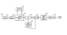
- the frequency synchronization apparatus for an orthogonal frequency division multiplexing (OFDM) communication system comprises, a radio frequency (RF) receiving module for receiving OFDM signal, an analog/digital (A/D) converter connected to the RF receiving module, the A/D converter converting the OFDM signal into a digital signal, a frequency synchronization module connected to the A/D converter, a Fast Fourier Transformer (FFT) connected to the frequency synchronization module, a channel estimation module connected to the FFT, an equalizer connected to the FFT and the channel estimation module, a residual phase tracking module connected to the equalizer, a demodulator connected to the residual phase tracking module, and a controller connected to the frequency synchronization module.
- RF radio frequency
- A/D analog/digital
- FFT Fast Fourier Transformer
- FIG. 1 a is a block diagram showing a frequency synchronization apparatus in the orthogonal frequency division multiplexing (OFDM) communication system according to a preferred embodiment of the present invention
- FIG. 1 b is a block diagram showing a frequency synchronization module of the frequency offset synchronization apparatus of FIG. 1 a;
- FIG. 1 c is a block diagram showing a residual phase tracking module of the frequency synchronization apparatus of FIG. 1 a;
- FIG. 1 d is a block diagram illustrating the operation of the frequency synchronization part of FIG. 1 b when using a single training signal
- FIG. 1 e is a block diagram illustrating the operation of the residual phase tracking module of FIG. 1 c when a pilot signal is set to a predetermined value
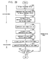
- FIG. 2 a is a flow chart illustrating a frequency synchronization method of the OFDM communication system according to the referred embodiment of the present invention when using two training signals;
- FIG. 2 b is a flow chart illustrating the frequency synchronization method of the OFDM communication when using one training signal
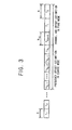
- FIG. 3 shows a structure of the training signal according to the preferred embodiment of the present invention
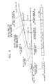
- FIG. 4 is a drawing illustrating effects of the frequency offsets and an initial phase at the point of frequency compensation
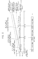
- FIG. 5 is a drawing illustrating effects of carrier frequency offsets of data symbol periods
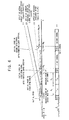
- FIG. 6 is a drawing illustrating effects of the carrier frequency offsets and an initial phase at the point of frequency compensation when a single step frequency offset synchronization method is used with a single training signal;
- FIG. 7 shows graphs for illustrating an implementation of an arctangent table according to the preferred embodiment of the present invention.
- FIG. 8 is a drawing for illustrating a phase adjustment method according to the preferred embodiment of the present invention.
- FIG. 9 a pair of drawings showing the sine and cosine waveforms
- FIG. 10 is a drawing illustrating an operation of a bit expander of the frequency synchronization apparatus of FIG. 1;
- FIG. 11 is a drawing for illustrating address generation in a sine and cosine tables in accordance with region.
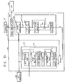
- FIG. 1 a , FIG. 1 b , and FIG. 1 c are respective block diagrams showing a frequency synchronization apparatus in the orthogonal frequency division multiplexing (OFDM) communication system according to a preferred embodiment of the present invention, frequency offset synchronization module of the frequency synchronization apparatus of FIG. 1 a , a residual phase tracking module of the frequency synchronization apparatus of FIG. 1 a .
- FIG. 1 d and FIG. 1 e are respective block diagrams illustrating the operation of the frequency synchronization module of FIG. 1 b when using a single training signal, a block diagram illustrating the operation of the residual phase tracking module of FIG. 1 c when a pilot signal is set to a predetermined value.
- the frequency synchronization apparatus comprises a radio frequency (RF) receiving module 100 for receiving an OFDM signal transmitted by an OFDM transmitter, an A/D converter 200 connected to the RF receiving module 100 for converting the OFDM signal into a digital signal, a frequency synchronization module 300 connected to the A/D converter 200 for synchronizing a carrier frequency, a Fast Fourier Transformer (FFT) 400 connected to the frequency synchronization module 300 for performing the fast Fourier transformation on every symbol therefrom, a channel estimation module 450 connected to the FFT 400 for estimating channel, an equalizer 500 connected to the FFT 400 , a residual phase tracking module 600 connected to the equalizer 500 for estimating the residual phase, and a demodulator 700 connected to the residual phase tracking module 600 for demodulating the modulated signal so as to reproduce the original signal.
- RF radio frequency
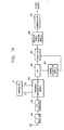
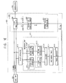
- the frequency synchronization module 300 comprises an estimation submodule 310 for estimating a frequency offset and residual phase of the received signal, a first demultiplexer 330 for selectively outputting the frequency offset and residual phase in accordance with a control signal from the controller 10 , an adder 340 for adding the frequency offset from the estimation submodule, a frequency offset compensation submodule 320 for compensating the received signal and data symbol using the frequency offsets from the first demultiplexer 330 the adder 340 , and a second demultiplexer 350 for selectively outputting the signal from the frequency offset compensation submodule 320 according to the control signal from the controller 10 .
- the estimation submodule 310 comprises a shift register part 311 for delaying a sample of the training signal and outputting conjugate complex numbers of a predetermined training signal and a following training signal at the same time, and a selective estimation part 312 for estimating the frequency offset of the signal from the shift register part 311 and a residual phase of the signal from the residual phase tracking module 600 .
- the selective estimation part 312 comprises a first multiplier 312 - 1 for multiplying the signals from the shift register part 311 or the residual phase tracking module 600 , a first accumulator 312 - 2 for accumulating the samples obtained by calculation of the first conjugated complex number multiplier 312 - 1 , a divider 312 - 3 for generating arctangent table address on the basis of ratio of a real part to imaginary part of a value accumulated at the accumulator 312 - 2 , an arctangent table 312 - 4 stored arctangent values sampled in a predetermined interval so as to output a corresponding arctangent value to the arctangent table address generated by the divider, and a phase converter 312 - 5 for converting the arctangent value into a value of a corresponding region by referring to a sign of the accumulated value at the first accumulator 312 - 2 and outputting the value as an estimated frequency offset.
- the arctangent values are classified into values of predetermined regions and the values in a representative one of the regions stored as representative values in the arctangent table 3124 .
- the frequency offset compensation submodule 320 comprises a bit expander 321 for dividing the estimated frequency offset into samples of a predetermined size, a second accumulator for generating a first log function table address by accumulating frequency offset of each sample obtained at the bit expander 321 , a first region controller 323 for identifying a sign of value at the bit expander and converting the first log function table address into a corresponding address value in a predetermined region and outputting the same, a first log function table 324 for outputting the log function value stored by sampling in a predetermined distance in accordance with the address value outputted from the first region controller 323 , and a second multiplier 325 for compensating the frequency offset by multiplying the training signal or data symbol by the log function value outputted from the first log function table 324 .
- the sine and cosine values are divided into predetermined regions and one of the region is divided by a predetermined value and stored in the first log function table 324 .
- the first region controller 323 outputs an address value resulting from a subtraction of a predetermined value from the output value and then shift the present region to a next region. Also, the first region controller 323 outputs the output value of the second accumulator 322 using complementary operation for obtaining a sine or cosine value in a symmetric region.
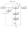
- the residual phase tracking module 600 estimates a residual phase using the selective estimation part 312 of the frequency offset synchronization module 300 .
- the residual phase tracking module 600 comprises a pilot extractor 610 for extracting a pilot signal from the data symbol transformed by the Fourier Transform operation and sending the pilot signal to the selective estimation part 312 , and a residual phase compensation part 620 for compensating the data symbol with the residual phase of the data symbol estimated at the selective estimation part 312 .
- the residual phase tracking module 620 comprises a second region controller 621 for outputting a second log function table address corresponding to the residual phase value outputted from the first demultiplexer 330 , a second log function table 622 for outputting a previously stored log function value, which is obtained by sampling in a predetermined interval, corresponding to the log function table address from the second region controller, and a third multiplier 623 for compensating the residual phase by multiplying the log function value outputted from the second log function table 622 with the compensated data symbol.
- the sine and cosine values are divided into predetermined regions and then one of the regions is divided by a predetermined value so as to be stored in the second table 622 .
- the second region controller 621 outputs an address resulting from subtracting a predetermined value from the output value and then shifts the present address region to a next address region if the output value from the first demultiplexer 330 is greater than the predetermined value. Also, the second region controller 621 outputs an address obtained from the first demultiplexer 330 through a complementary operation for calculating the sine and cosine values in symmetry region.
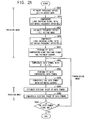
- FIG. 2 a and FIG. 2 b are flow charts illustrating frequency synchronization method of the OFDM communication system respectively when using two training signals and using one training signal.
- the frequency synchronization method of the OFDM communication system comprises the steps of (A) estimating and compensating the frequency offset of the training signal, performing the Fast Fourier Transform (FFT), and estimating a channel (S 800 ⁇ S 840 ); (B) compensating the data symbol of the received signal with the frequency offset estimated at step (A), performing the FFT, and then compensating the data symbol with the channel estimated at step (A) (S 850 ⁇ S 870 ); and (C) estimating and compensating a residual phase of the channel-compensated data symbol (S 880 ⁇ 895 ).
- FFT Fast Fourier Transform
- the step (A) comprises the sub-steps of (A1) estimating the frequency offset using a short training signal and compensating a long training signal with the estimated frequency offset when the received signal has the two kinds of training signals (S 800 ⁇ S 810 ; coarse mode), (A2) re-estimating the frequency offset of the long training signal compensated at the sub-step A1 and re-compensating the long training signal (S 820 ⁇ 830 ; fine mode).
- step (B) the data symbol is compensated by multiplying the exponential function with the frequency offsets estimated at the sub-steps (A1) and (A2), i.e., at the coarse and fine modes.
- the sub-step (A1) comprises the stages of (A1-1) performing a conjugate complex number computation and accumulation thereof by delaying a sample of the short training signal, creating an arctangent table address by obtaining a ratio of real and imaginary parts of the accumulated value; and (A1-2) outputting estimated frequency offset by identifying a code of the accumulated value and transforming the arctangent value according to the arctangent table address to a corresponding region value; (A1-3) dividing the estimated frequency offset into predetermined sizes, accumulating them, and creating a first log function table address; (A1-4) transforming the first log function table address into a corresponding region address by identifying the accumulated code value of the stage (A1-3) and then outputting a log function value corresponding to the transformed address; and (A1-5) compensating the frequency offset by multiplying the long training signal with the log function value outputted at the stage (A1-4) (not shown).
- the stage (A1-1) has a sub-stage of dividing the arctangent value into a predetermined regions and then dividing one of the regions by a predetermined value so as to be previously stored in the arctangent table.
- the stage (A1-4) has a sub-stage of dividing the sine and cosine values into the predetermined regions and then one of the regions by a predetermined value so as to be previously stored in the first log function table, and outputting the sine and cosine values corresponding to the value resulting from subtracting a predetermined value from the accumulated value and shifting the present address region to the next region if the accumulated value is greater than the predetermined value.
- the address value created for obtaining the sine or cosine value of the symmetric region is outputted after the complementary operation.
- the sub-step (A2) comprises the stages of (A2-1) creating an arctangent table address by delaying sample of the frequency-compensated long training signal and performing the conjugate complex number calculation and accumulation thereof and obtaining the ratio of the real and imaginary parts of the accumulated value, (A2-2) outputting the estimated frequency offset by identifying the code of the accumulated value and transforming the arctangent value of the arctangent table address to the corresponding region value, (A2-3) accumulating the estimated frequency offset after dividing in the predetermined size and creating the log function table address, (A2-4) transforming the first log function table address to the corresponding region address by identifying the accumulated code value of the stage (A2-3) and then outputting the log function value corresponding to the transformed address, and (A2-5) compensating the frequency offset by multiplying the log function value outputted at the stage (A2-4) with the frequency-compensated long training signal of the step (A1) (not shown).
- the stage (A2-1) has sub-stage of dividing the arctangent value into predetermined regions and then dividing one of the regions by a predetermined value so as to be previously stored in the arctangent table.
- the stage (A2-4) has a sub-stage of dividing the sine and cosine values into the predetermined regions and then one of the regions by a predetermined value so as to be previously stored in the first log function table, and outputting the sine and cosine values corresponding to the value resulting from subtracting a predetermined value from the accumulated value and shifting the present address region to the next region if the accumulated value is greater than the predetermined value.
- the address value created for obtaining the sine or cosine value of the symmetric region is outputted after the complementary operation.
- the step (C) comprises the sub-steps of (C1) performing the conjugate complex number calculation and accumulation of pilot signals extracted from the compensated data symbols and creating arc tangent table address by calculating the ratio of the real and imaginary parts of the accumulated value, (C2) outputting the estimated residual phase by identifying the code of the accumulated value and transforming the arctangent value of the arctangent table address to the corresponding region value, (C3) creating the second log function table address according to the estimated residual phase estimated at the sub-step (C2) and outputting the corresponding log function value, and (C4) compensating the residual phase by multiplying the data symbol with the log function value outputted at the sub-step (C3).
- the sub-step (C1) has a sub-stage of dividing the arctangent value into predetermined regions and then dividing one of the regions by a predetermined value so as to previously store in the arctangent table.
- the stage (C3) has a sub-stage of dividing the sine and cosine values into the predetermined regions and then one of the regions by a predetermined value so as to be previously stored in the first log function table, and outputting the sine and cosine values corresponding to the value resulting from subtracting a predetermined value from the accumulated value and shifting the present address region to the next region if the accumulated value is greater than the predetermined value.
- the address value created for obtaining the sine or cosine value of the symmetric region is outputted after the complementary operation.
- FIG. 3 shows a structure of the training signal according to the preferred embodiment of the present invention.
- the training signal used in the OFDM wireless modem includes continuous N s short training signals (t 1 ⁇ t Ns ) of sample length D, continuous two long training signals (T 1 , T 2 ) of sample length N, and a guard interval (T GUARD ) interposed between the sets of short and long training signals.
- the OFDM training structure of the IEEE 802.11a wireless LAN consists of 10 short training symbols and two long training symbols.
- a guard interval interposes between the sets of the short and long training symbols.
- FIG. 4 is a drawing illustrating effects of the frequency offsets and an initial phase at the point of frequency offset compensation.
- the carrier frequency synchronization method will be described with reference to FIG. 4 and through the mathematical signal analysis.
- the short training signal of the OFDM communication system is generated according to the equation 1.
- S s (k) is the short training symbol and N is the size of the FFT/IFFT.
- the short symbol s s (n) of the period D repeats N/D times in time domain such that the short training symbols are transmitted with repetition of N s , times.
- the short training symbol can be expressed as the following equation when the effect of the frequency offset is included.
- ⁇ f is subcarrier spacing
- H(k) is channel response
- 2 ⁇ t/N is initial phase rotation
- N c is a coarse mode start point
- W(n) is an added noise.
- the auto correlation characteristic of the short training symbols t Ns ⁇ 1 ⁇ t Ns is used for coarsely performing carrier frequency synchronization.
- the signal received at the RF module 100 is sent to the shift register part 311 via the A/D converter 200 and then the shift register part 311 delays the training symbol in the received signal such that the conjugate complex numbers of the t Ns ⁇ i and t Ns ⁇ i ⁇ 1 are inputted to the first multiplier 312 - 1 at the same time.
- the conjugate complex numbers are multiplied in the conjugate complex number multiplier 312 - 1 and then the output values from the conjugate complex number multiplier 312 - 1 are accumulated in the accumulator 312 - 2 during the period of (i+1)*D.
- the “i” becomes 0 such that the accumulation is performed during the period of D
- three short training symbols are used, the “i” becomes 2 such that the accumulation is performed during the period of 2D.
- the accumulated value is divided into the real and imaginary parts so as to calculate a ratio of the real part to the imaginary part such that an arc tangent table address is created using the ratio in the first divider 312 - 3 . Consequently, the arctangent table address is stored in the argent table 312 - 4 in a predetermined sampling interval.
- the phase converter 312 - 5 identifies the codes of the real and imaginary parts of the accumulated value by referring to the divider 312 - 3 so as to transform the arctangent value outputted from the arctangent table 312 - 4 into the corresponding region value and then outputs the carrier frequency offset, ⁇ acute over ( ⁇ ) ⁇ c, which is calculated by equation 3. Finally, the carrier frequency offset is estimated by multiplying the period N/D.
- D is a distance between two symbols.
- the estimation range of the coarse frequency offset obtained using the auto correlation after delaying the training signal sample using short training symbols is
- the interval D is 16 such that carrier estimation range of the coarse mode is
- the average can be taken i ⁇ 1 times such that the frequency offset estimated by taking the averages of i ⁇ 1 times is more accurate than that of the frequency offset obtained using just two short training signals.
- the frequency offset can be obtained by averaging the sum of the auto correlation value between the first and second short training symbols and the auto correlation value between the second and third short training symbols.
- the frequency offset estimation must be performed in such a manner that the carrier frequency offset is roughly estimated in the coarse mode and then the frequency offset range of the long training symbol is narrowed using the estimated frequency offset of the coarse mode.
- the long training symbol received through the channel is determined as equation 4.
- the frequency offset value estimated at the frequency offset estimator 310 is inputted into the first demultiplexer 330 such that the demultiplexer 330 sends the demultiplexed signals to the bit expander 321 according to the control signal S 1 from the controller 10 .
- the signal ⁇ acute over ( ⁇ ) ⁇ will be exemplary described without subscript for the notational convenience.
- the signal from the demultiplexer 330 is shifted as much as log 2 N in the rightward direction at the bit expander 321 in order to divide the estimated value from the estimation part 310 into the sample size N for the FFT 400 .
- Each sample is accumulated at the second accumulator 322 such that the corresponding log function table address is assigned to the sample.
- the log function table address assigned at the accumulator 322 is transformed into an address in the corresponding range by referring to the code values of the bit expander 321 in the first region controller 323 such that the log function value stored in the address of the first log function table 324 is outputted.
- the log function value from the first log function table 324 is multiplied by the long training signal T 1 (T 2 ) from the A/D converter 200 in the second multiplier 325 so as to compensate frequency offset.
- the signal compensated by the estimated frequency offset is sent to the frequency offset compensator 310 and the second multiplier 325 by the second demultiplexer 350 according to the control signal S 2 from the controller 10 .
- the long training symbol digitally compensated by the carrier frequency offset estimator in the coarse mode, at step 820 can be expressed as equation 5.
- the frequency offset is precisely estimated in the fine mode at step S 820 .
- the frequency offset estimation in the fine mode is performed in the same manner as the frequency offset estimation in the coarse mode.
- the shift register part 311 delays the input signal as much as sample size N, and the block used in the coarse mode for estimating the coarse frequency offset is adopted in the following procedures.
- the frequency offset can be estimated using equation 6 where the noise is ignored, and the autocorrelation of the long training signal compensated in the coarse mode is used.
- the frequency offset ⁇ acute over ( ⁇ ) ⁇ f estimated in the fine mode is more accurate than that estimated in the coarse mode because more samples are used to obtain an average even though the estimation range is reduced to ⁇ 0.5 ⁇ acute over ( ⁇ ) ⁇ f ⁇ 0.5.
- the long training signal from the second demultiplexer 350 is compensated again using the frequency offset ⁇ acute over ( ⁇ ) ⁇ f estimated at the fine mode in the frequency offset compensation module 320 at step S 830 .
- the signal can be digitally compensated using the frequency offset estimator with a broad estimation range and high precision using the coarse and fine modes.
- the coarse and fine modes share the same hardware for frequency offset estimation operation.
- the long training signal compensated according to equation 7 is transformed in the FFT 400 , and the channel estimator 450 estimates the coefficients of the equalizer 500 using the zero-forcing method at step S 840 .
- the channel estimate ⁇ I (k) includes the initial phase rotation amont 2 ⁇ t, and a fine mode initial rotation amount 2 ⁇ n f /N.
- the complete digital compensation of the signal can be achieved since the data symbol is compensated together with the initial phase rotation amount included in the channel estimates, even though it is difficult to estimate the initial phase rotation amount because it is unable to calculate a start point thereof.
- the next data symbol inputted to the second multiplier 325 from the A/D converter 200 is compensated using the log function value corresponding to the frequency offset ⁇ acute over ( ⁇ ) ⁇ acute over ( ⁇ ) ⁇ f + ⁇ acute over ( ⁇ ) ⁇ c resulting from multiplying the frequency offset estimated in the fine and coarse modes in the adder 340 such that the carrier frequency synchronization is achieved at step S 850 .
- the adder 340 adds the frequency offsets estimated in the coarse and fine modes and sends the result to the bit expander according to the control signal S 1 from the controller 10 .
- the following processes are same in both coarse and fine mode.
- X i (k) is the data transmitted on the ith subcarrier
- Hi(k) is the channel response
- n d is an index where the data symbol compensation starts in time domain
- N G is the size of guard interval
- the positions of channel estimation using the long training signal and the data compensation using the estimated carrier frequency offset are not identical. Therefore, after data symbols compensated by the frequency offset estimator are transformed using FFT 400 at step S 860 and then compensated using the estimated channel in the equalizer 500 at step S 870 , the same phase rotation occurs to all the data symbols.
- the phase rotation can be compensated by the Frequency Domain Equalizer (FEQ) 500 .
- FIG. 4 is a drawing illustrating the effects of the frequency offsets and an initial phase at the frequency offset compensation point
- FIG. 5 is a drawing illustrating the effects of carrier frequency offsets of the data symbols.
- the residual frequency offset exists such that the phase rotation by the residual frequency offset gives critical effect to the data symbol if the received symbols is over a predetermined number.
- X ⁇ ⁇ ( k ) ⁇ Y i ⁇ ( k ) H ⁇ ⁇ ( k ) ⁇ ⁇ X i ⁇ ( k ) ⁇ H i ⁇ ( k ) ⁇ ⁇ j2 ⁇ ⁇ ( ⁇ - ⁇ ⁇ ) ⁇ ⁇ N ⁇ ( i - 1 ) + iN G ⁇ + j ⁇ ⁇ ( ⁇ - ⁇ ) ⁇ ( N - 1 ) N ⁇ ⁇ j2 ⁇ ⁇ ⁇ ⁇ ⁇ ( n d + ⁇ ⁇ ⁇ t ) N H l ⁇ ( k ) ⁇ j ⁇ ⁇ ( ⁇ - ⁇ ) ⁇ ( N - 1 ) N ⁇ ⁇ j2 ⁇ ⁇ ⁇ ⁇ ⁇ ( n d + ⁇ ⁇ ⁇ t ) N ⁇ X i ⁇ ( k ) ⁇
- the channel estimation position n f is not identical to the data symbol compensation position n d , leading to the phase rotation as much as j2 ⁇ (n d ⁇ n ⁇ )/N. Note that the phase rotation caused by the residual frequency offset increases in proportional to the symbol index i.
- the index increases from 0 while the compensations of the long training signal and the data symbol in the time domain such that the phase to be compensated for each sample can be obtained only using the accumulator and there is no need to calculate presently how many sample periods are far from the point of signal reception.
- phase rotation at equation 12 is estimated in such a manner of estimating the phase rotation caused by the residual frequency offset in the residual estimation part 600 together with the phase rotation amount for compensating the effect of the residual frequency offset after passing the equalizer 500 . Accordingly, there is no need of the additional hardware for compensating the phase rotation because the data symbol is compensated by increasing the index from 0 in time domain.
- the residual estimation part 600 extracts pilot signal of each symbol in the tracking mode and compensates, in frequency domain, the phase rotation caused by the residual frequency offset existing even after the compensation of carrier frequency using the autocorrelation.
- a pilot extractor 610 of the residual phase estimation part 600 extracts the pilot signal and sends the pilot signal to the first multiplier 312 - 1 of the selective estimation part 312 such that the selective estimation part 312 estimates the phase rotation caused by the difference between the point of the residual frequency and channel estimation and the point of the data symbol compensation in time domain at step S 880 .
- the residual phase offset can be calculated using the autocorrelation of the pilot signal in the tracking mode as equation 13.
- X i (p) is the P th pilot signal of the i th OFDM symbol.
- a second region controller 621 of the residual compensation part 620 generates a second log function table address corresponding to the residual phase value from the first demultiplexer 330 of the selective estimator 312 .
- the second log function table 622 outputs one of the log function values which is sampled in a predetermined interval and stored therein according to the second log function address from the second region controller 621 and the third multiplier 623 compensates the log function value from the second log function table 622 by multiplying the log function value with the compensated data symbol at step S 890 .
- the signal passed through the residual phase compensation part 620 shows that the phase rotation caused by the difference between the residual frequency offset/channel estimation point and the data symbol compensation point is compensated.
- the selective estimation part 312 is shared for reducing the hardware needed for residual phase tracking in the preferred embodiment of the present invention, another circuit identical to the selective estimation part 312 can be implemented.
- FIG. 6 is a drawing illustrating effects of the carrier frequency offsets and an initial phase at an offset compensation point in a single step frequency offset synchronization method using one type training signal.
- FIG. 1 d is a block diagram illustrating the operation of the frequency synchronization part of FIG. 1 b when using single training signal.
- the adder 340 and the second demultiplexer 350 are not depicted for simplifying the drawing.
- the training signal consists of T t1 and T t2 each having D t samples.
- the training signal can be expressed as equation 15.
- n 0,1,2, . . . ,2D t ⁇ 1
- S t (k) is the training signal in the frequency domain and H t (k) is the frequency response of the long training signal.
- the carrier frequency offset is estimated using the autocorrelation of the received signals at step S 900 .
- the frequency offset can be expressed as equation 16.
- the carrier frequency offset estimation range is ⁇ ⁇ ⁇ t ⁇ ⁇ N / 2 ⁇ D t
- n 0,1,2, . . . ,2D t ⁇ 1
- the channel estimation is performed on the basis of the FFT and zero forcing at step S 920 .
- the effect of the residual frequency offset remained in the training signal during the channel estimation can be approximated as in equation 18 where only the phase is distorted.
- H ⁇ i ⁇ ( k ) ⁇ FFT ⁇ ( y i ⁇ ( n ) ) S i ⁇ ( k ) ⁇ ⁇ H i ⁇ ( k ) ⁇ ⁇ j ⁇ ⁇ ( ⁇ - ⁇ ⁇ ) ⁇ ( N - 1 ) N ⁇ ⁇ j2 ⁇ ⁇ ⁇ ⁇ ⁇ ⁇ ⁇ ⁇ ⁇ t N Equation ⁇ ⁇ 18
- [0152] is the phase rotation caused by the residual frequency offset. Since the channel estimation value ⁇ t (k) includes the initial phase rotation amount 2 ⁇ ⁇ ⁇ ⁇ ⁇ ⁇ ⁇ t N
- an unknown initial phase rotation can be compensated if the data symbol is compensated using the channel estimation value, resulting in complete digital compensation.
- the channel estimation point and the compensation point is same such that the phase rotation caused by the difference between the channel estimation and channel compensation points does not exist.
- the i th received OFDM data symbol including the guard interval can be expressed as equation 19 after compensation of carrier frequency offset ⁇ circumflex over ( ⁇ ) ⁇ t .
- n 0,1, . . . , N+N G ⁇ 1
- X i (k) is a signal in the frequency range of the i th data
- H i (k) is the frequency response of the i th data symbol
- n t is the carrier frequency offset estimation-beginning point.
- X ⁇ i ⁇ ( k ) ⁇ ⁇ FFT ⁇ ( y i ⁇ ( n ) ) H ⁇ t ⁇ ( k ) ⁇ ⁇ X i ⁇ ( k ) ⁇ H i ⁇ ( k ) ⁇ ⁇ j2 ⁇ ⁇ ( ⁇ - ⁇ ⁇ i ) ⁇ ⁇ N ⁇ ( i - 1 ) + iN G + n i ⁇ + j ⁇ ⁇ ( ⁇ - ⁇ ) ⁇ ( N - 1 ) N ⁇ ⁇ j2 ⁇ ⁇ ⁇ ⁇ ⁇ ⁇ ⁇ ⁇ t N H t ⁇ ( k ) ⁇ j ⁇ ⁇ ( ⁇ - ⁇ ) ⁇ ( N - 1 ) N ⁇ ⁇ j2 ⁇ ⁇ ⁇ ⁇ ⁇ ⁇ ⁇ ⁇ ⁇ t N ⁇ j2 ⁇ ⁇ ⁇ ⁇ ⁇ ⁇
- [0160] is the initial phase generated by deleting the guard interval of the i th OFDM symbol.
- the residual frequency is very small since the data symbol is the result compensated by the estimated carrier frequency offset.
- phase tracking process for compensating the phase rotation caused by the residual frequency is performed using pilot signal included in each data symbol.
- the phase rotation caused by the residual frequency is estimated using the autocorrelation of the pilot signals at step S 960 .
- the phase rotation can be expressed as equation 21.
- ⁇ circumflex over (X) ⁇ t (p) is the p th pilot signal in the received signal ⁇ circumflex over (X) ⁇ t (k) and X t (p) is the p th pilot symbol of the i th transmitted OFDM symbol.
- the estimated phase rotation is compensated at step S 970 and the compensated signal can be expressed as equation 22.
- X ⁇ i ⁇ ( k ) ⁇ X ⁇ i ⁇ ( k ) ⁇ ⁇ - j ⁇ ⁇ ⁇ i N ⁇ ⁇ X i ⁇ ( k ) Equation ⁇ ⁇ 22
- the same hardware and processes can be used in the two step method using long training and short training signals and the one step method just using short training signal or even when using short training signal in case of additional training signal being for channel estimation.
- the hardware complexity and the computation accuracy of the apparatus and method for OFDM frequency synchronization of the present invention depends on the arctangent table 312 - 4 and the log function tables. Accordingly, it is need to reduce the size of the tables and enhance the computation accuracy.
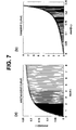
- FIG. 7 shows graphs for illustrating the implementation of an arctangent table according to the present invention.
- the tangent curve repeats 4 times in its shape in the range of [ ⁇ ⁇ ] with different signs. Accordingly, in the present invention the tangent curve in the range of [0 ⁇ /2] is stored in the table and the arctangent value outputted from the phase converter 312 - 5 according to the signs of the real and imaginary parts of the divider 312 - 3 .
- an arctangent input range corresponding to the output range [0 ⁇ /2] is [0 ⁇ 8].
- the arctangent input is limited to the range of [0 ⁇ 8] (see FIG. 7 a ) and it is preferred to take graded samples according to the gradient of the arctangent.
- [0174] is multiplied to the carrier frequency offset. To remove this, the data is stored after multiplied by 1 2 ⁇ ⁇
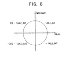
- FIG. 8 is a drawing for illustrating a phase adjustment method of the present invention.
- the phase converter 312 - 5 outputs arctangent values using the signs of the real and imaginary parts of the accumulated data from the divider 312 - 3 .
- phase adjustment standard is not 1 ⁇ 2 ⁇ but just 1 ⁇ 2 is because the output range of the arc tangent table 312 - 4 is [0 ⁇ 1 ⁇ 4].
- N/D is multiplied to the arctangent output when estimating the frequency offset in the coarse mode such that in the coarse mode the arctangent output is shifted as much as 2 bits in leftward direction.
- an arithematical bit expansion should be executed in addition to the 2-bit shift for preventing the accuracy of the arctangent from being fallen.
- the arctangent table implemented as above has a small hardware complexity and can be used in the coarse and fine modes in the same manner. Furthermore, since the outputs of the divider 312 - 3 correspond to the arctangent table addresses, there is no need of additional hardware for creating addresses.
- the output of the frequency offset compensation module can be expressed as equation 23.
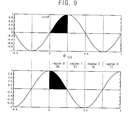
- the log function table consists of sine and cosine table so as to create output at every clock tick.
- FIG. 9 is a pair of drawings showing the sine and cosine waveforms. As shown in FIG. 9, each of the sine and cosine curves has a wavelength which is divided into 4 regions numbered from 0 to 3. Once the log function table is created using function values in the range of [0 ⁇ /2], i.e., region 0 , the function values in other regions 1 , 2 and 3 can be obtained using the function values of region 0 .
- [0186] corresponds to the addresses in the sine and cosine tables and if ⁇ ⁇ ⁇ ⁇ n N
- the estimated frequency offset ⁇ circumflex over ( ⁇ ) ⁇ is accumulated in the second accumulator 322 at every clock ticks such that the second accumulator 322 creates addresses of the log function table.
- the bit expander 321 previously divides estimation value by N such that the number of bits of the second accumulator 322 can be fixed.
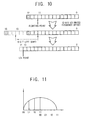
- FIG. 10 is a drawing for illustrating the operation of a bit expander of the frequency synchronization apparatus of the present invention.
- the output from the second accumulator cannot be a value in other ranges. That is, if the result of accumulation to the n ⁇ 1, ⁇ ⁇ ⁇ ⁇ ( n - 1 ) N ,
- [0197] can exist in the region 0 or region 1 , but not in the region 3 or region 2 .
- region is a present region.
- the first region controller 323 identifies the output from the second accumulator 322 and bypasses the output if the output is less than 1 ⁇ 4. On the other hand, if the output is greater than 1 ⁇ 4, the first region controller 323 generates an output by subtracting 1 ⁇ 4 from the output and shifts the present region to next region.
- the output of the second accumulator 322 is greater than 1 ⁇ 4 such that the first region controller 323 can be simply implemented by resetting the fourteenth bit position to 0 and shifting the region.
- the function values in the region 2 where only the sign is opposite to that of the region 0 is simply obtained using the function values of the region 0 . Even though the function values of the region 1 and region 3 that are symmetrically positioned to the region 0 are impossible to be directly obtained using the table, the cosine and sine values can be obtained from respective sine and cosine tables without changing the tables.
- FIG. 11 is a drawing for illustrating address creation in a sine and cosine tables in accordance with region.
- FIG. 1 e is a block diagram for illustrating the residual phase tracking part wherein the imaginary part of the pilot signal is 0 and the real part of the pilot signal is 0, 1, or ⁇ 1.
- the residual phase compensation part 620 has a similar structure with the frequency synchronization module 300 . Since the estimation module 310 is used in initial synchronization, the estimation module is shared by the residual phase estimation part as explained above.
- the first conjugate complex number multiplier 312 - 1 can be replaced by a sign changing part 313 . That is, the sign changing part 313 outputs 0 if the real part of the pilot signal is 0, outputs the input data as it is if the real part is 1, and outputs the input data after changing its sign into opposite sign if the real part is ⁇ 1.
- the residual phase compensation part 620 differs from the frequency offset compensation module 320 except for the sine and cosine tables. Furthermore, since the frequency offset compensation module 320 must constantly compensate the input data symbol, it can be shared by the residual phase compensation part 620 . Accordingly, the residual phase compensation part 620 can be simply implemented relative to the frequency offset compensation module 320 because the phase inputted to the sine and cosine tables are not changed in one symbol time even though the residual phase compensation part 620 has the sine and cosine tables.
- the frequency offset estimation accuracy is enhanced as well as the frequency offset estimation range is expanded to ⁇ ⁇ ⁇ ⁇ ⁇ N 2 ⁇ D ,
- the hardware used in the two-step estimation method can be used in the one-step estimation method using just one kind of training signal.
- the initial phase rotation amount 2 ⁇ t is estimated when the channel is estimated such that the initial phase rotation amount can be compensated in the frequency domain equalizer.
- phase rotation j2 ⁇ ⁇ ( n d - n f ) N ,
- estimation part and the frequency offset compensation module are shared by the residual phase tracking part in the tracking mode such that the overall implementation space of the frequency synchronization apparatus can be reduced, leading to the increase of synchronization speed.
- the frequency offset estimation and frequency synchronization circuit can be separated from analog domain part, resulting in reduction of overall manufacturing cost and high integration of the circuit.
Abstract
Description
- (a) Field of the Invention
- The present invention relates to an apparatus and method for frequency synchronization, and in particular, to an apparatus and method for completely synchronizing carrier frequency through a digital process in an orthogonal frequency division multiplexing (OFDM) wireless communication system.
- (b) Description of the Related Art
- In OFDM, original data stream is multiplexed into N parallel data streams each of the data streams modulated with a different frequency using an Inverse Fast Fourier Transform (IFFT), and the resulting signals are transmitted together in the same band.
- The OFDM symbols are artificially prolonged by periodically repeating a guard interval which is longer than a maximum channel delay so as to remove the reflections of previous symbols, which preserves the orthogonality such that inter symbol interferences (ISI) and inter channel interference are reduced.
- Successful OFDM reception requires that a receiver maintains correct symbol synchronization which means that the receiver knows at which point of time each symbol begins and ends.
- Maintaining the symbol synchronization is difficult if a transmitter and receiver are moving with respect to each other. For example, if a mobile station moves around in an urban environment, the propagation path of the signal changes constantly, resulting in attenuation and reflection. Also, the mobile station moving fast causes phase jitter and Doppler shift, resulting in frequency offset which means difference in frequency between the transmitter and receiver. This frequency offset causes inter symbol interference and damages the orthogonality condition required among the subcarriers, resulting in degradation of bit error rate.
- Accordingly, in order for the receiver to be able to successfully receive the symbols, the receiver has to synchronize carrier frequency between the transmitter and receiver before performing the Fast Fourier Transform (FFT).
- To reduce the carrier frequency offset, a wireless modem adopting the OFDM modulation sends a training signal for channel estimation and initial frequency synchronization. The Wireless Local Area Network standards such as the HIPERLAN/2 developed by the European Telecommunications Standards Institute (ETSI) and the 802.11a of the Institute of Electrical and Electronics Engineers (IEEE) specify a short training sequence in which 16 samples are repeated 10 times and a long training sequence in which 64 time samples are repeated twice.
- In the conventional synchronization method, the frequency synchronization device estimates the carrier frequency offsets using the training signals in digital domain and passes the signals through a loop filter so as to control a voltage controlled oscillator (VCO) such that the VCO output is used to synchronize the carrier frequency in analog domain.
- In other cases, especially for single carrier transmission, a numerical controlled oscillator (NCO) is used for compensating the frequency offset in the digital domain.
- However, in the carrier frequency synchronization method of the conventional OFDM system in which the carrier frequency synchronization is performed in analog domain, it is impossible to perform a precise carrier frequency synchronization since the carrier frequency synchronization is performed using the output of the VCO that is controlled by the signal generated by the estimated frequency offsets and this causes the synchronization time delay.
- Also, in the conventional method, since the carrier frequency offset is estimated in digital domain and the frequency offset is compensated using the VCO in analog domain, its implementation and performance analysis are difficult in this mixed analog-digital mode.
- As the implementation method for obtaining an arctangent and exponential function for synchronizing carrier frequency in digital domain, the techniques employing the Coordinate Rotation Digital Computer (CORDIC) and Look-up table are used.
- However, the CORDIC method has a drawback in that the computing speed is slow and the precision is low despite of its simple implementation. On the other hand, the look-up table method requires lots of memory modules causing a hardware complexity and it is difficult to create addresses in look-up table in spite of its fast speed and high precision.
- The present invention has been made in an effort to solve the above problems of the prior art.
- It is an object of the present invention to provide a frequency synchronization apparatus and method for the orthogonal frequency division multiplexing (OFDM) communication system capable of synchronizing carrier frequency while maintaining a high precision of data reception regardless of the time delay by compensating frequency offsets in the digital domain.
- It is another object of the present invention to provide a frequency synchronization apparatus and method for the OFDM communication system capable of precisely estimating the frequency offset in a broad estimation range using a coarse and fine modes.
- It is another object of the present invention to provide a frequency synchronization apparatus and method for the OFDM communication system capable of tracking a residual phase by implementing the same hardware used in the coarse and fine mode estimation circuits so as to share in parts.
- It is still another object of the present invention to provide a frequency synchronization apparatus and method for the OFDM communication system capable of performing computation with a high precision in simple hardware using a look-up table containing arctangent and log functions required for estimating and compensating the frequency offset.
- To achieve the above objects, the frequency synchronization apparatus for an orthogonal frequency division multiplexing (OFDM) communication system according to the present invention comprises, a radio frequency (RF) receiving module for receiving OFDM signal, an analog/digital (A/D) converter connected to the RF receiving module, the A/D converter converting the OFDM signal into a digital signal, a frequency synchronization module connected to the A/D converter, a Fast Fourier Transformer (FFT) connected to the frequency synchronization module, a channel estimation module connected to the FFT, an equalizer connected to the FFT and the channel estimation module, a residual phase tracking module connected to the equalizer, a demodulator connected to the residual phase tracking module, and a controller connected to the frequency synchronization module.
- The accompanying drawings, which are incorporated in and constitute a part of the specification, illustrate an embodiment of the invention, and together with the description, serve to explain the principles of the invention.
- FIG. 1 a is a block diagram showing a frequency synchronization apparatus in the orthogonal frequency division multiplexing (OFDM) communication system according to a preferred embodiment of the present invention;
- FIG. 1 b is a block diagram showing a frequency synchronization module of the frequency offset synchronization apparatus of FIG. 1a;
- FIG. 1 c is a block diagram showing a residual phase tracking module of the frequency synchronization apparatus of FIG. 1a;
- FIG. 1 d is a block diagram illustrating the operation of the frequency synchronization part of FIG. 1b when using a single training signal;
- FIG. 1 e is a block diagram illustrating the operation of the residual phase tracking module of FIG. 1c when a pilot signal is set to a predetermined value;
- FIG. 2 a is a flow chart illustrating a frequency synchronization method of the OFDM communication system according to the referred embodiment of the present invention when using two training signals;
- FIG. 2 b is a flow chart illustrating the frequency synchronization method of the OFDM communication when using one training signal;
- FIG. 3 shows a structure of the training signal according to the preferred embodiment of the present invention;
- FIG. 4 is a drawing illustrating effects of the frequency offsets and an initial phase at the point of frequency compensation;
- FIG. 5 is a drawing illustrating effects of carrier frequency offsets of data symbol periods;
- FIG. 6 is a drawing illustrating effects of the carrier frequency offsets and an initial phase at the point of frequency compensation when a single step frequency offset synchronization method is used with a single training signal;
- FIG. 7 shows graphs for illustrating an implementation of an arctangent table according to the preferred embodiment of the present invention;
- FIG. 8 is a drawing for illustrating a phase adjustment method according to the preferred embodiment of the present invention;
- FIG. 9 a pair of drawings showing the sine and cosine waveforms;
- FIG. 10 is a drawing illustrating an operation of a bit expander of the frequency synchronization apparatus of FIG. 1; and
- FIG. 11 is a drawing for illustrating address generation in a sine and cosine tables in accordance with region.
- A preferred embodiment of the present invention will be described hereinafter with reference to the accompanying drawings. A frequency synchronization apparatus and method of the present invention will be explained by embodying in an OFDM wireless modem.
- FIG. 1 a, FIG. 1b, and FIG. 1c are respective block diagrams showing a frequency synchronization apparatus in the orthogonal frequency division multiplexing (OFDM) communication system according to a preferred embodiment of the present invention, frequency offset synchronization module of the frequency synchronization apparatus of FIG. 1a, a residual phase tracking module of the frequency synchronization apparatus of FIG. 1a. FIG. 1d and FIG. 1e are respective block diagrams illustrating the operation of the frequency synchronization module of FIG. 1b when using a single training signal, a block diagram illustrating the operation of the residual phase tracking module of FIG. 1c when a pilot signal is set to a predetermined value.
- Referring to FIG. 1 a˜FIG. 1c, the frequency synchronization apparatus comprises a radio frequency (RF) receiving
module 100 for receiving an OFDM signal transmitted by an OFDM transmitter, an A/D converter 200 connected to theRF receiving module 100 for converting the OFDM signal into a digital signal, afrequency synchronization module 300 connected to the A/D converter 200 for synchronizing a carrier frequency, a Fast Fourier Transformer (FFT) 400 connected to thefrequency synchronization module 300 for performing the fast Fourier transformation on every symbol therefrom, achannel estimation module 450 connected to theFFT 400 for estimating channel, anequalizer 500 connected to theFFT 400, a residualphase tracking module 600 connected to theequalizer 500 for estimating the residual phase, and ademodulator 700 connected to the residualphase tracking module 600 for demodulating the modulated signal so as to reproduce the original signal. - The
frequency synchronization module 300 comprises anestimation submodule 310 for estimating a frequency offset and residual phase of the received signal, afirst demultiplexer 330 for selectively outputting the frequency offset and residual phase in accordance with a control signal from thecontroller 10, anadder 340 for adding the frequency offset from the estimation submodule, a frequency offsetcompensation submodule 320 for compensating the received signal and data symbol using the frequency offsets from thefirst demultiplexer 330 theadder 340, and asecond demultiplexer 350 for selectively outputting the signal from the frequency offsetcompensation submodule 320 according to the control signal from thecontroller 10. - The
estimation submodule 310 comprises ashift register part 311 for delaying a sample of the training signal and outputting conjugate complex numbers of a predetermined training signal and a following training signal at the same time, and aselective estimation part 312 for estimating the frequency offset of the signal from theshift register part 311 and a residual phase of the signal from the residualphase tracking module 600. - The
selective estimation part 312 comprises a first multiplier 312-1 for multiplying the signals from theshift register part 311 or the residualphase tracking module 600, a first accumulator 312-2 for accumulating the samples obtained by calculation of the first conjugated complex number multiplier 312-1, a divider 312-3 for generating arctangent table address on the basis of ratio of a real part to imaginary part of a value accumulated at the accumulator 312-2, an arctangent table 312-4 stored arctangent values sampled in a predetermined interval so as to output a corresponding arctangent value to the arctangent table address generated by the divider, and a phase converter 312-5 for converting the arctangent value into a value of a corresponding region by referring to a sign of the accumulated value at the first accumulator 312-2 and outputting the value as an estimated frequency offset. - It is preferred that the arctangent values are classified into values of predetermined regions and the values in a representative one of the regions stored as representative values in the arctangent table 3124.
- The frequency offset
compensation submodule 320 comprises abit expander 321 for dividing the estimated frequency offset into samples of a predetermined size, a second accumulator for generating a first log function table address by accumulating frequency offset of each sample obtained at thebit expander 321, afirst region controller 323 for identifying a sign of value at the bit expander and converting the first log function table address into a corresponding address value in a predetermined region and outputting the same, a first log function table 324 for outputting the log function value stored by sampling in a predetermined distance in accordance with the address value outputted from thefirst region controller 323, and asecond multiplier 325 for compensating the frequency offset by multiplying the training signal or data symbol by the log function value outputted from the first log function table 324. - It is preferred that the sine and cosine values are divided into predetermined regions and one of the region is divided by a predetermined value and stored in the first log function table 324.
- The
first region controller 323 outputs an address value resulting from a subtraction of a predetermined value from the output value and then shift the present region to a next region. Also, thefirst region controller 323 outputs the output value of thesecond accumulator 322 using complementary operation for obtaining a sine or cosine value in a symmetric region. - The residual
phase tracking module 600 estimates a residual phase using theselective estimation part 312 of the frequency offsetsynchronization module 300. The residualphase tracking module 600 comprises apilot extractor 610 for extracting a pilot signal from the data symbol transformed by the Fourier Transform operation and sending the pilot signal to theselective estimation part 312, and a residualphase compensation part 620 for compensating the data symbol with the residual phase of the data symbol estimated at theselective estimation part 312. - The residual
phase tracking module 620 comprises asecond region controller 621 for outputting a second log function table address corresponding to the residual phase value outputted from thefirst demultiplexer 330, a second log function table 622 for outputting a previously stored log function value, which is obtained by sampling in a predetermined interval, corresponding to the log function table address from the second region controller, and athird multiplier 623 for compensating the residual phase by multiplying the log function value outputted from the second log function table 622 with the compensated data symbol. - The sine and cosine values are divided into predetermined regions and then one of the regions is divided by a predetermined value so as to be stored in the second table 622.
- The
second region controller 621 outputs an address resulting from subtracting a predetermined value from the output value and then shifts the present address region to a next address region if the output value from thefirst demultiplexer 330 is greater than the predetermined value. Also, thesecond region controller 621 outputs an address obtained from thefirst demultiplexer 330 through a complementary operation for calculating the sine and cosine values in symmetry region. - FIG. 2 a and FIG. 2b are flow charts illustrating frequency synchronization method of the OFDM communication system respectively when using two training signals and using one training signal.
- Referring to FIG. 2 a, the frequency synchronization method of the OFDM communication system comprises the steps of (A) estimating and compensating the frequency offset of the training signal, performing the Fast Fourier Transform (FFT), and estimating a channel (S800˜S840); (B) compensating the data symbol of the received signal with the frequency offset estimated at step (A), performing the FFT, and then compensating the data symbol with the channel estimated at step (A) (S850˜S870); and (C) estimating and compensating a residual phase of the channel-compensated data symbol (S880˜895).
- The step (A) comprises the sub-steps of (A1) estimating the frequency offset using a short training signal and compensating a long training signal with the estimated frequency offset when the received signal has the two kinds of training signals (S 800˜S810; coarse mode), (A2) re-estimating the frequency offset of the long training signal compensated at the sub-step A1 and re-compensating the long training signal (S820˜830; fine mode).
- At step (B), the data symbol is compensated by multiplying the exponential function with the frequency offsets estimated at the sub-steps (A1) and (A2), i.e., at the coarse and fine modes.
- The sub-step (A1) comprises the stages of (A1-1) performing a conjugate complex number computation and accumulation thereof by delaying a sample of the short training signal, creating an arctangent table address by obtaining a ratio of real and imaginary parts of the accumulated value; and (A1-2) outputting estimated frequency offset by identifying a code of the accumulated value and transforming the arctangent value according to the arctangent table address to a corresponding region value; (A1-3) dividing the estimated frequency offset into predetermined sizes, accumulating them, and creating a first log function table address; (A1-4) transforming the first log function table address into a corresponding region address by identifying the accumulated code value of the stage (A1-3) and then outputting a log function value corresponding to the transformed address; and (A1-5) compensating the frequency offset by multiplying the long training signal with the log function value outputted at the stage (A1-4) (not shown).
- The stage (A1-1) has a sub-stage of dividing the arctangent value into a predetermined regions and then dividing one of the regions by a predetermined value so as to be previously stored in the arctangent table.
- The stage (A1-4) has a sub-stage of dividing the sine and cosine values into the predetermined regions and then one of the regions by a predetermined value so as to be previously stored in the first log function table, and outputting the sine and cosine values corresponding to the value resulting from subtracting a predetermined value from the accumulated value and shifting the present address region to the next region if the accumulated value is greater than the predetermined value.
- At the stage (A1-3), the address value created for obtaining the sine or cosine value of the symmetric region is outputted after the complementary operation.
- The sub-step (A2) comprises the stages of (A2-1) creating an arctangent table address by delaying sample of the frequency-compensated long training signal and performing the conjugate complex number calculation and accumulation thereof and obtaining the ratio of the real and imaginary parts of the accumulated value, (A2-2) outputting the estimated frequency offset by identifying the code of the accumulated value and transforming the arctangent value of the arctangent table address to the corresponding region value, (A2-3) accumulating the estimated frequency offset after dividing in the predetermined size and creating the log function table address, (A2-4) transforming the first log function table address to the corresponding region address by identifying the accumulated code value of the stage (A2-3) and then outputting the log function value corresponding to the transformed address, and (A2-5) compensating the frequency offset by multiplying the log function value outputted at the stage (A2-4) with the frequency-compensated long training signal of the step (A1) (not shown).
- The stage (A2-1) has sub-stage of dividing the arctangent value into predetermined regions and then dividing one of the regions by a predetermined value so as to be previously stored in the arctangent table.
- The stage (A2-4) has a sub-stage of dividing the sine and cosine values into the predetermined regions and then one of the regions by a predetermined value so as to be previously stored in the first log function table, and outputting the sine and cosine values corresponding to the value resulting from subtracting a predetermined value from the accumulated value and shifting the present address region to the next region if the accumulated value is greater than the predetermined value.
- At the stage (A2-3), the address value created for obtaining the sine or cosine value of the symmetric region is outputted after the complementary operation.
- The step (C) comprises the sub-steps of (C1) performing the conjugate complex number calculation and accumulation of pilot signals extracted from the compensated data symbols and creating arc tangent table address by calculating the ratio of the real and imaginary parts of the accumulated value, (C2) outputting the estimated residual phase by identifying the code of the accumulated value and transforming the arctangent value of the arctangent table address to the corresponding region value, (C3) creating the second log function table address according to the estimated residual phase estimated at the sub-step (C2) and outputting the corresponding log function value, and (C4) compensating the residual phase by multiplying the data symbol with the log function value outputted at the sub-step (C3).
- The sub-step (C1) has a sub-stage of dividing the arctangent value into predetermined regions and then dividing one of the regions by a predetermined value so as to previously store in the arctangent table.
- The stage (C3) has a sub-stage of dividing the sine and cosine values into the predetermined regions and then one of the regions by a predetermined value so as to be previously stored in the first log function table, and outputting the sine and cosine values corresponding to the value resulting from subtracting a predetermined value from the accumulated value and shifting the present address region to the next region if the accumulated value is greater than the predetermined value.
- At the stage (C3), the address value created for obtaining the sine or cosine value of the symmetric region is outputted after the complementary operation.
- The frequency synchronization method of the present invention will be described, in more detail, with reference to the FIG. 1 a˜FIG. 11 hereinafter.
- So far, a frequency synchronization method of synchronizing carrier frequency offset using the short and long training signals is described in two-step full digital approach. The general techniques used in the front-end of the receiver such as signal detection and sensing the start of symbol are not explained here.
- FIG. 3 shows a structure of the training signal according to the preferred embodiment of the present invention.
- As shown in FIG. 3, the training signal used in the OFDM wireless modem includes continuous N s short training signals (t1˜tNs) of sample length D, continuous two long training signals (T1, T2) of sample length N, and a guard interval (TGUARD) interposed between the sets of short and long training signals.
- For example, the OFDM training structure of the IEEE 802.11a wireless LAN consists of 10 short training symbols and two long training symbols. A guard interval interposes between the sets of the short and long training symbols.
- FIG. 4 is a drawing illustrating effects of the frequency offsets and an initial phase at the point of frequency offset compensation. The carrier frequency synchronization method will be described with reference to FIG. 4 and through the mathematical signal analysis.
- Firstly, the short training signal of the OFDM communication system according to the preferred embodiment of the present invention is generated according to the
equation 1.
- where S s(k) is the short training symbol and N is the size of the FFT/IFFT.
- The short symbol s s(n) of the period D repeats N/D times in time domain such that the short training symbols are transmitted with repetition of Ns, times.
- Since the signal may experience the phase jitter and Doppler shift during the propagation, the short training symbol can be expressed as the following equation when the effect of the frequency offset is included.

- where ε (=f offset/Δf) is a normalized frequency offset and foffset is a frequency offset, Δf is subcarrier spacing, and H(k) is channel response Δt is a signal reception start point (n=0), 2πΔt/N is initial phase rotation, Nc is a coarse mode start point, and W(n) is an added noise.
- As shown in
equation 2, since the received signal rs(n) of the period D repeats N/D times, an approximate frequency offset can be estimated using the auto correlation characteristic in the coarse mode at step S800. - In the coarse mode, the auto correlation characteristic of the short training symbols t Ns−1˜tNs is used for coarsely performing carrier frequency synchronization.
- The signal received at the
RF module 100 is sent to theshift register part 311 via the A/D converter 200 and then theshift register part 311 delays the training symbol in the received signal such that the conjugate complex numbers of the tNs−i and tNs−i−1 are inputted to the first multiplier 312-1 at the same time. The conjugate complex numbers are multiplied in the conjugate complex number multiplier 312-1 and then the output values from the conjugate complex number multiplier 312-1 are accumulated in the accumulator 312-2 during the period of (i+1)*D. In the coarse mode, if two short training symbols are used, the “i” becomes 0 such that the accumulation is performed during the period of D, and three short training symbols are used, the “i” becomes 2 such that the accumulation is performed during the period of 2D. - Next, the accumulated value is divided into the real and imaginary parts so as to calculate a ratio of the real part to the imaginary part such that an arc tangent table address is created using the ratio in the first divider 312-3. Consequently, the arctangent table address is stored in the argent table 312-4 in a predetermined sampling interval.
- The phase converter 312-5 identifies the codes of the real and imaginary parts of the accumulated value by referring to the divider 312-3 so as to transform the arctangent value outputted from the arctangent table 312-4 into the corresponding region value and then outputs the carrier frequency offset, {acute over (ε)}c, which is calculated by
equation 3. Finally, the carrier frequency offset is estimated by multiplying the period N/D.
- where D is a distance between two symbols.
- As shown in
equation 3, the estimation range of the coarse frequency offset obtained using the auto correlation after delaying the training signal sample using short training symbols is |{acute over (ε)}c|<N/2D and the estimation accuracy depends on L(the number of samples). For example, in the IEEE 802.11a wireless LAN, the interval D is 16 such that carrier estimation range of the coarse mode is |{acute over (ε)}c|<2. However, the estimation accuracy is low because the sample of L=N/4 taking an average is relatively small. - On the other hand, if the value L is greater than the interval D between the two repeating symbols when estimating the frequency offset using more than 3 short training symbol in
equation 3, the number of the samples used for frequency offset estimation increases so as to reduce the noise such that the estimation range is maintained in |{acute over (ε)}c|<N/2D and the estimation accuracy is improved. - In the case where the frequency offset is estimated using the number of i short training symbols repeated in N/D times, the average can be taken i−1 times such that the frequency offset estimated by taking the averages of i−1 times is more accurate than that of the frequency offset obtained using just two short training signals.
- For example, if the carrier frequency offset is estimated using 3 short training symbols and L is 2D, the frequency offset can be obtained by averaging the sum of the auto correlation value between the first and second short training symbols and the auto correlation value between the second and third short training symbols.
- Since it is impossible to know how large the frequency offset is generated in the real environment, the frequency offset estimation must be performed in such a manner that the carrier frequency offset is roughly estimated in the coarse mode and then the frequency offset range of the long training symbol is narrowed using the estimated frequency offset of the coarse mode.
- The long training symbol received through the channel is determined as
equation 4.
- where S 1 is a long training symbol, H1(k) is a frequency response of the channel, and nf is a start point of the fine mode. In
equation 4, r1 (n) composed of N samples repeats twice. - The frequency offset value estimated at the frequency offset
estimator 310 is inputted into thefirst demultiplexer 330 such that thedemultiplexer 330 sends the demultiplexed signals to thebit expander 321 according to the control signal S1 from thecontroller 10. In FIG. 1b, since the demultiplexed signals are processed with the same procedure after the bit expending process, the signal {acute over (ε)} will be exemplary described without subscript for the notational convenience. - The signal from the
demultiplexer 330 is shifted as much as log2N in the rightward direction at thebit expander 321 in order to divide the estimated value from theestimation part 310 into the sample size N for theFFT 400. Each sample is accumulated at thesecond accumulator 322 such that the corresponding log function table address is assigned to the sample. - The log function table address assigned at the
accumulator 322 is transformed into an address in the corresponding range by referring to the code values of thebit expander 321 in thefirst region controller 323 such that the log function value stored in the address of the first log function table 324 is outputted. - The log function value from the first log function table 324 is multiplied by the long training signal T1(T2) from the A/
D converter 200 in thesecond multiplier 325 so as to compensate frequency offset. - The signal compensated by the estimated frequency offset is sent to the frequency offset
compensator 310 and thesecond multiplier 325 by thesecond demultiplexer 350 according to the control signal S2 from thecontroller 10. - The long training symbol digitally compensated by the carrier frequency offset estimator in the coarse mode, at
step 820, can be expressed asequation 5.
- In
equation 5, the residual frequency offset {acute over (ε)}−{acute over (ε)}c exists, when the long training signal is compensated by the frequency offset {acute over (ε)}c estimated in the coarse mode. - Next, by using the compensated long training signal, the frequency offset is precisely estimated in the fine mode at step S 820. The frequency offset estimation in the fine mode is performed in the same manner as the frequency offset estimation in the coarse mode. In this case, the
shift register part 311 delays the input signal as much as sample size N, and the block used in the coarse mode for estimating the coarse frequency offset is adopted in the following procedures. - The frequency offset can be estimated using
equation 6 where the noise is ignored, and the autocorrelation of the long training signal compensated in the coarse mode is used.
- In
equation 6, the frequency offset {acute over (ε)}f estimated in the fine mode is more accurate than that estimated in the coarse mode because more samples are used to obtain an average even though the estimation range is reduced to−0.5<{acute over (ε)}f<0.5. - Accordingly, the long training signal from the
second demultiplexer 350 is compensated again using the frequency offset {acute over (ε)}f estimated at the fine mode in the frequency offsetcompensation module 320 at step S830. - The signal compensated by the frequency offset estimator in the fine mode is expressed as
equation 7.
- As described above, in the frequency synchronization method of the present invention, the signal can be digitally compensated using the frequency offset estimator with a broad estimation range and high precision using the coarse and fine modes. The coarse and fine modes share the same hardware for frequency offset estimation operation.
- The long training signal compensated according to
equation 7 is transformed in theFFT 400, and thechannel estimator 450 estimates the coefficients of theequalizer 500 using the zero-forcing method at step S840. - To simplify the mathematical expression, it is assumed that the effects of noise and residual frequency offset ε−{acute over (ε)} c are ignorable. In this case, the amplitude distortion is reduced because the residual frequency offset is very small so that only the phase distortion remains.
- Accordingly, the effects of the residual frequency offset remaining in the long training signal after the initial synchronization can be approximated to the following form distorted just in phase as the
equation 8 if the effect from the noise is ignored.
- In the
equation 8, the channel estimate ĤI(k) includes the initial phase rotation amont 2πεΔt, and a fine mode initial rotation amount 2πεnf/N. The complete digital compensation of the signal can be achieved since the data symbol is compensated together with the initial phase rotation amount included in the channel estimates, even though it is difficult to estimate the initial phase rotation amount because it is unable to calculate a start point thereof. - The next data symbol inputted to the
second multiplier 325 from the A/D converter 200 is compensated using the log function value corresponding to the frequency offset {acute over (ε)}≈{acute over (ε)}f+{acute over (ε)}c resulting from multiplying the frequency offset estimated in the fine and coarse modes in theadder 340 such that the carrier frequency synchronization is achieved at step S850. In this case theadder 340 adds the frequency offsets estimated in the coarse and fine modes and sends the result to the bit expander according to the control signal S1 from thecontroller 10. The following processes are same in both coarse and fine mode. - When the data symbol is compensated using the log function value corresponding to the address {acute over (ε)}≈{acute over (ε)} f+{acute over (ε)}c, an ith OFDM symbol is expressed as equation 9.

- where X i(k) is the data transmitted on the ith subcarrier, Hi(k) is the channel response, nd is an index where the data symbol compensation starts in time domain, and NG is the size of guard interval.
- As indicated in the equation 9 and FIG. 4, the positions of channel estimation using the long training signal and the data compensation using the estimated carrier frequency offset are not identical. Therefore, after data symbols compensated by the frequency offset estimator are transformed using
FFT 400 at step S860 and then compensated using the estimated channel in theequalizer 500 at step S870, the same phase rotation occurs to all the data symbols. The phase rotation can be compensated by the Frequency Domain Equalizer (FEQ) 500. - FIG. 4 is a drawing illustrating the effects of the frequency offsets and an initial phase at the frequency offset compensation point, and FIG. 5 is a drawing illustrating the effects of carrier frequency offsets of the data symbols.
- As shown in FIG. 4, even though the data symbol is compensated through the two step compensation method, the residual frequency offset exists such that the phase rotation by the residual frequency offset gives critical effect to the data symbol if the received symbols is over a predetermined number.
- In this case, since the residual frequency offset remained in the i th OFDM symbol received during the initial synchronization process is very small, the signal transformed in the FFT after deleting the guard interval from the ith OFDM symbol can be expressed as
equation 10, where the noise is ignored for simplifying the equation.
- where e Jπε(n d )+Δt/N is the initial phase where the data symbol begins, and ej2π(ε−{circumflex over (ε)} t ){N(t−1)+iN G }/N is the initial phase rotation caused by deleting the guard interval of the ith data symbol.
- The channel distortion is compensated using the channel value estimated by
equation 8. Supposed that the channel experienced by the long training signal and the channel of the data sequence are identical, i.e., H1(k)=Hi(k), the equation can be simplified asequation 11.
- If the residual frequency offset is 0 in
equation 11, it can be much simplified as following equation.
- As shown in
equation 11 andequation 12, the channel estimation position nf is not identical to the data symbol compensation position nd, leading to the phase rotation as much as j2πε(nd−nƒ)/N. Note that the phase rotation caused by the residual frequency offset increases in proportional to the symbol index i. - On the other hand, if the data symbol is compensated in such a manner that the channel is estimated using the long training signal of which the carrier frequency offset is compensated in the condition of n=n f when n=0, and the index is increased from n=nd, then the phase rotation problem in
equation 11 can be solved. - However, since the phase to be compensated is j2π{circumflex over (ε)}n ƒ if the index is increased from n=nf and when n is 0, additional hardware is required because the accumulator adds nf or the multiplier should be used to obtain the phase.
- In the present invention, the index increases from 0 while the compensations of the long training signal and the data symbol in the time domain such that the phase to be compensated for each sample can be obtained only using the accumulator and there is no need to calculate presently how many sample periods are far from the point of signal reception.
- The phase rotation at
equation 12 is estimated in such a manner of estimating the phase rotation caused by the residual frequency offset in theresidual estimation part 600 together with the phase rotation amount for compensating the effect of the residual frequency offset after passing theequalizer 500. Accordingly, there is no need of the additional hardware for compensating the phase rotation because the data symbol is compensated by increasing the index from 0 in time domain. - The
residual estimation part 600 extracts pilot signal of each symbol in the tracking mode and compensates, in frequency domain, the phase rotation caused by the residual frequency offset existing even after the compensation of carrier frequency using the autocorrelation. - A
pilot extractor 610 of the residualphase estimation part 600 extracts the pilot signal and sends the pilot signal to the first multiplier 312-1 of theselective estimation part 312 such that theselective estimation part 312 estimates the phase rotation caused by the difference between the point of the residual frequency and channel estimation and the point of the data symbol compensation in time domain at step S880. The residual phase offset can be calculated using the autocorrelation of the pilot signal in the tracking mode asequation 13.
- where (p) is the p th pilot signal in the received signal

- (k), and

- X i(p) is the Pth pilot signal of the ith OFDM symbol.
- As shown in
equation 13, when estimating the phase rotation by the residual frequency using the autocorrelation of the pilot signal in the tracking mode, the phase rotation caused by difference between the channel estimation point and the data symbol compensation point is also estimated. - A
second region controller 621 of theresidual compensation part 620 generates a second log function table address corresponding to the residual phase value from thefirst demultiplexer 330 of theselective estimator 312. - The second log function table 622 outputs one of the log function values which is sampled in a predetermined interval and stored therein according to the second log function address from the
second region controller 621 and thethird multiplier 623 compensates the log function value from the second log function table 622 by multiplying the log function value with the compensated data symbol at step S890. - The data symbol compensated in the residual
phase compensation part 620 using the phase rotation value estimated to every symbols in thepilot extractor 610 and theestimation part 310 is expressed asequation 14.
- In
equation 14, the signal passed through the residualphase compensation part 620 shows that the phase rotation caused by the difference between the residual frequency offset/channel estimation point and the data symbol compensation point is compensated. - The residual phase compensated-signal loops from the step S 850 to the step S895 until it is to be the last data symbol, and then is sent to a viterbi decoder via a
demodulator 700. - Even though the
selective estimation part 312 is shared for reducing the hardware needed for residual phase tracking in the preferred embodiment of the present invention, another circuit identical to theselective estimation part 312 can be implemented. - Also, in the OFDM wireless burst modem using one of the training signals, its frequency synchronization method is similar to the 2 step method and the same hardware can be used.
- FIG. 6 is a drawing illustrating effects of the carrier frequency offsets and an initial phase at an offset compensation point in a single step frequency offset synchronization method using one type training signal. In this case the procedure for synchronizing the carrier frequency offset using one type training signal is same with the frequency synchronization method of FIG. 2 b without the coarse mode, i.e., {circumflex over (ε)}=0.
- FIG. 1 d is a block diagram illustrating the operation of the frequency synchronization part of FIG. 1b when using single training signal. In FIG d the
adder 340 and thesecond demultiplexer 350 are not depicted for simplifying the drawing. - Referring to FIG. 1 d and FIG. 6, the training signal consists of Tt1 and Tt2 each having Dt samples. In this case the training signal can be expressed as
equation 15.
- n=0,1,2, . . . ,2D t−1
- where S t(k) is the training signal in the frequency domain and Ht(k) is the frequency response of the long training signal. Δt is the beginning point (n=0) of the signal reception and 2πΔt/N is the initial phase rotation.
- Since the same signals are repeatedly received in D t samples, the carrier frequency offset is estimated using the autocorrelation of the received signals at step S900. The frequency offset can be expressed as equation 16.

- In equation 16, the carrier frequency offset estimation range is

- when using one type training signal. In the case of D t=D<N, the estimation range is

- which is the same as the estimation result obtained by using the short training signal in the 2 step frequency offset synchronization as in
equation 3. - The signal compensated in the training signal and the data symbol using the estimated frequency offset {circumflex over (ε)} t can be expressed as equation 17.

- n=0,1,2, . . . ,2D t−1
- In equation 17, the channel can be estimated using the training signal when the training signal has only the long training signals, i.e., Dt=N. The channel estimation is performed on the basis of the FFT and zero forcing at step S 920. In this case, since the effects of noise is ignored and the training signal is compensated using the estimated carrier frequency offset, the effect of the residual frequency offset remained in the training signal during the channel estimation can be approximated as in
equation 18 where only the phase is distorted.
- k=0,1, . . . , N−1
- where

- is the phase rotation caused by the residual frequency offset. Since the channel estimation value Ĥ t(k) includes the initial
phase rotation amount 
- like in
equation 8, an unknown initial phase rotation can be compensated if the data symbol is compensated using the channel estimation value, resulting in complete digital compensation. - In the synchronization method using only one type training signal, the channel estimation point and the compensation point is same such that the phase rotation caused by the difference between the channel estimation and channel compensation points does not exist.
- The i th received OFDM data symbol including the guard interval can be expressed as equation 19 after compensation of carrier frequency offset {circumflex over (ε)}t.

- n=0,1, . . . , N+N G−1
- where X i(k) is a signal in the frequency range of the ith data, Hi(k) is the frequency response of the ith data symbol, and nt is the carrier frequency offset estimation-beginning point.
- The frequency offset compensated-data symbol is transformed in the FFT at step S 940, and the ith OFDM data symbol is equalized using the estimated channel value in the
equalizer 500 at step S950. In this case, supposed that the effect of the noise is ignored and the channel does not change, i.e., HI(k)=Hi(k), the equation can be simplified as equation 20.
- where

- is the initial phase generated by deleting the guard interval of the i th OFDM symbol. In equation 20, the residual frequency is very small since the data symbol is the result compensated by the estimated carrier frequency offset.
- In comparison between
equation 11 and equation 20, there is no phase rotation ej2πε(n d−nƒ )/N in one step method as expressed byequation 11 because the channel estimation and compensation is performed at the same position. On the other hand, the phase rotation caused by the residual frequency offset increases in proportional to the symbol index i in the two step method as expressed by equation 20 such that the effect of the residual frequency offset causes critical problem after the number of predetermined symbols. - Accordingly, the phase tracking process for compensating the phase rotation caused by the residual frequency is performed using pilot signal included in each data symbol. The phase rotation caused by the residual frequency is estimated using the autocorrelation of the pilot signals at step S 960. The phase rotation can be expressed as equation 21.

- where {circumflex over (X)} t(p) is the pth pilot signal in the received signal {circumflex over (X)}t(k) and Xt(p) is the pth pilot symbol of the ith transmitted OFDM symbol.
- The estimated phase rotation is compensated at step S 970 and the compensated signal can be expressed as equation 22.

- As shown in equation 22, it is possible to digitally synchronize carrier frequency in the one step method using only the long training signal of D t=N through the same processes as in the two step method.
- In case only the short training signal of D t=D is used, a measure for estimating the channel is considered even though the processes for estimating and compensating the frequency offset are same with the method using only the long training signal. Generally, since the D samples become non-zero value and N−D samples become zeros if the repeated signals are transformed by the FFT, it is impossible to calculate the channel just using the short training signal relative to all the sub-channels on the basis of the zero forcing. In this case, channel estimation should be performed using special method such as an interpolation or another training signal should be adapted for estimating the channel.
- As explained above, in the apparatus and method for synchronizing frequency in the OFDM communication system, the same hardware and processes can be used in the two step method using long training and short training signals and the one step method just using short training signal or even when using short training signal in case of additional training signal being for channel estimation.
- How the arctangent function table and the first and second log function tables of the present invention are implemented will be described hereinafter.
- The hardware complexity and the computation accuracy of the apparatus and method for OFDM frequency synchronization of the present invention depends on the arctangent table 312-4 and the log function tables. Accordingly, it is need to reduce the size of the tables and enhance the computation accuracy.
- FIG. 7 shows graphs for illustrating the implementation of an arctangent table according to the present invention.
- Generally, the tangent curve repeats 4 times in its shape in the range of [−π˜π] with different signs. Accordingly, in the present invention the tangent curve in the range of [0˜π/2] is stored in the table and the arctangent value outputted from the phase converter 312-5 according to the signs of the real and imaginary parts of the divider 312-3.
- In this case an arctangent input range corresponding to the output range [0˜π/2] is [0˜8]. However, since over 90% of the arctangent outputs are concentrated in the input range of [0˜8], the arctangent input is limited to the range of [0˜8] (see FIG. 7 a) and it is preferred to take graded samples according to the gradient of the arctangent.
- In
equations 
- is multiplied to the carrier frequency offset. To remove this, the data is stored after multiplied by

- when arctangent table is implemented. Accordingly, the arctangent output range becomes [1˜¼].
- FIG. 8 is a drawing for illustrating a phase adjustment method of the present invention.
- As explained above, since the values in the range of [0˜π/2] are stored in the arctangent table, the phase converter 312-5 outputs arctangent values using the signs of the real and imaginary parts of the accumulated data from the divider 312-3.
- The reason why the phase adjustment standard is not ½π but just ½ is because the output range of the arc tangent table 312-4 is [0˜¼].
- While, a difference between the
equation equation 3, i.e., N/D is multiplied to the arctangent output when estimating the frequency offset in the coarse mode such that in the coarse mode the arctangent output is shifted as much as 2 bits in leftward direction. In this case an arithematical bit expansion should be executed in addition to the 2-bit shift for preventing the accuracy of the arctangent from being fallen. - The arctangent table implemented as above has a small hardware complexity and can be used in the coarse and fine modes in the same manner. Furthermore, since the outputs of the divider 312-3 correspond to the arctangent table addresses, there is no need of additional hardware for creating addresses.
- On the other hand, the output of the frequency offset compensation module can be expressed as equation 23.

- where {circumflex over (ε)} is an estimated frequency offset and has a value of {circumflex over (ε)}={circumflex over (ε)} c, {circumflex over (ε)}={circumflex over (ε)}f, {circumflex over (ε)}={circumflex over (ε)}ƒ+{circumflex over (ε)}c, and {circumflex over (ε)}={circumflex over (ε)}t according to the tracking mode. As shown in equation 23, the log function table consists of sine and cosine table so as to create output at every clock tick.
- FIG. 9 is a pair of drawings showing the sine and cosine waveforms. As shown in FIG. 9, each of the sine and cosine curves has a wavelength which is divided into 4 regions numbered from 0 to 3. Once the log function table is created using function values in the range of [0˜π/2], i.e.,
region 0, the function values inother regions region 0. - Also, in order to simply create the log function table, it is preferred to normalize the input values of the log function table to 2π such that the actual input range is to be [0˜¼].
- As such, 2π of the
equation 14 can be ignored such that the
- corresponds to the addresses in the sine and cosine tables and if

- becomes greater than ¼ the region is shifted.
- The estimated frequency offset {circumflex over (ε)} is accumulated in the
second accumulator 322 at every clock ticks such that thesecond accumulator 322 creates addresses of the log function table. In this case thebit expander 321 previously divides estimation value by N such that the number of bits of thesecond accumulator 322 can be fixed. - FIG. 10 is a drawing for illustrating the operation of a bit expander of the frequency synchronization apparatus of the present invention.
- Let's suppose that the estimated frequency offset is expressed in 13 bits, 3 bits are located left side of a floating point, and the most left bit is a sign bit.
- The estimated frequency offset is shifted 6 positions to the left so as to be divided by N(=64).
- Next, the left bits from the point of ¼ is removed and 15 bits of

- is outputted. The output of the second accumulator can be expressed as equation 24.

- As described above, since the input range of the sine and cosine table is [0˜¼], accurate sine and cosine function values cannot be obtained if the output from the
second accumulator 322 is out of the range. However, the output value from thesecond accumulator 322 increases due to the every clock accumulation and this problem is solved by thefirst region controller 323. - Since the estimated frequency offset is inputted to the
second accumulator 322 after being divided by N, the output from the second accumulator cannot be a value in other ranges. That is, if the result of accumulation to the n−1,
- is in the
region 0, the accumulation result to n,
- can exist in the
region 0 orregion 1, but not in theregion 3 orregion 2. The region shift depends on whether the accumulation result is greater than ¼ or not. This can be expressed as equation 25.
- region=region+1
- else

- end,
- where “region” is a present region.
- The
first region controller 323 identifies the output from thesecond accumulator 322 and bypasses the output if the output is less than ¼. On the other hand, if the output is greater than ¼, thefirst region controller 323 generates an output by subtracting ¼ from the output and shifts the present region to next region. - In FIG. 10, if the fourteenth position bit is 1 on actually implementing hardware, the output of the
second accumulator 322 is greater than ¼ such that thefirst region controller 323 can be simply implemented by resetting the fourteenth bit position to 0 and shifting the region. - Also, the function values in the
region 2 where only the sign is opposite to that of theregion 0 is simply obtained using the function values of theregion 0. Even though the function values of theregion 1 andregion 3 that are symmetrically positioned to theregion 0 are impossible to be directly obtained using the table, the cosine and sine values can be obtained from respective sine and cosine tables without changing the tables. - This will be explained with an example of a table having a
size 4 with reference to FIG. 11. FIG. 11 is a drawing for illustrating address creation in a sine and cosine tables in accordance with region. - In FIG. 11, if the output of the
second accumulator 322 is in theregion 0 and the value of the output is 11, the next output of thesecond accumulator 322 becomes 100 such that thefirst region controller 323 performs region control. However, the output value of theaddress 11 is not obtained since the value of theaddress 00 is 0. - While, as explained in FIG. 7 the data of
address 00 in theregion 1 is identical to the data ofaddress 11 in the log function table, the data ofaddress 10 in theregion 1 is identical to the data ofaddress 01 in the log function table. That is, the output of thesecond accumulator 322 must be complemented before being stored as an address in the log function table. In this manner, the function values of all the regions can be obtained using the lookup table implemented with theregion 0. - By implementing the frequency offset compensation module according to the above explained method, the hardware size can be reduced.
- FIG. 1 e is a block diagram for illustrating the residual phase tracking part wherein the imaginary part of the pilot signal is 0 and the real part of the pilot signal is 0, 1, or −1.
- In FIG. 1 e, the residual
phase compensation part 620 has a similar structure with thefrequency synchronization module 300. Since theestimation module 310 is used in initial synchronization, the estimation module is shared by the residual phase estimation part as explained above. - In case that the imaginary part of the pilot signal is 0 and the real part of the pilot signal is 0, 1, or −1 as in the IEEE 802.11a wireless LAN, the first conjugate complex number multiplier 312-1 can be replaced by a
sign changing part 313. That is, thesign changing part 313outputs 0 if the real part of the pilot signal is 0, outputs the input data as it is if the real part is 1, and outputs the input data after changing its sign into opposite sign if the real part is −1. - On the other hand, the residual
phase compensation part 620 differs from the frequency offsetcompensation module 320 except for the sine and cosine tables. Furthermore, since the frequency offsetcompensation module 320 must constantly compensate the input data symbol, it can be shared by the residualphase compensation part 620. Accordingly, the residualphase compensation part 620 can be simply implemented relative to the frequency offsetcompensation module 320 because the phase inputted to the sine and cosine tables are not changed in one symbol time even though the residualphase compensation part 620 has the sine and cosine tables. - While this invention has been described in connection with what is presently considered to be the most practical and preferred embodiment, it is to be understood that the invention is not limited to the disclosed embodiments, but, on the equivalent arrangements included within the spirit and scope of the appended claims.
- As described above, in the apparatus and method for synchronizing frequency in OFDM communication, the frequency offset estimation accuracy is enhanced as well as the frequency offset estimation range is expanded to

- using the two-step estimation method with fine and coarse modes, such that the carrier frequency synchronization is completely performed in the digital domain.
- Also, the hardware used in the two-step estimation method can be used in the one-step estimation method using just one kind of training signal.
- Still more, even though the initial phase rotation amount 2πεΔt exists in data symbol, the initial phase rotation amount 2πεΔt is estimated when the channel is estimated such that the initial phase rotation amount can be compensated in the frequency domain equalizer.
- Also, in the present invention, the phase rotation,

- caused by the difference between the carrier frequency offset compensation point and the channel estimation point of the data symbol is estimated and compensated together with the phase rotation caused by the residual frequency in the residual phase estimation part in the tracking mode, such that the carrier frequency can be completely synchronized in the digital domain.
- Furthermore, the estimation part and the frequency offset compensation module are shared by the residual phase tracking part in the tracking mode such that the overall implementation space of the frequency synchronization apparatus can be reduced, leading to the increase of synchronization speed.
- Since the frequency offset estimation and frequency synchronization is performed in the digital domain, the frequency offset estimation and frequency synchronization circuit can be separated from analog domain part, resulting in reduction of overall manufacturing cost and high integration of the circuit.
Claims (39)
Applications Claiming Priority (2)
| Application Number | Priority Date | Filing Date | Title |
|---|---|---|---|
| KR2001-6196 | 2001-02-08 | ||
| KR10-2001-0006196A KR100402906B1 (en) | 2001-02-08 | 2001-02-08 | Frequency-offset synchronization apparatus and method for an ofdm |
Publications (2)
| Publication Number | Publication Date |
|---|---|
| US20020145971A1 true US20020145971A1 (en) | 2002-10-10 |
| US7068593B2 US7068593B2 (en) | 2006-06-27 |
Family
ID=19705507
Family Applications (1)
| Application Number | Title | Priority Date | Filing Date |
|---|---|---|---|
| US09/994,568 Expired - Fee Related US7068593B2 (en) | 2001-02-08 | 2001-11-26 | Apparatus and method for synchronizing frequency in orthogonal frequency division multiplexing communication system |
Country Status (2)
| Country | Link |
|---|---|
| US (1) | US7068593B2 (en) |
| KR (1) | KR100402906B1 (en) |
Cited By (42)
| Publication number | Priority date | Publication date | Assignee | Title |
|---|---|---|---|---|
| US20030128790A1 (en) * | 2001-06-20 | 2003-07-10 | Koninklijke Philips Electronics N.V. | Method of, and receiver for, minimising carrier phase rotation due to signal adjustments and enhancements |
| US20030227866A1 (en) * | 2002-06-06 | 2003-12-11 | Hirohisa Yamaguchi | Multi-path equalization for orthogonal frequency division multiplexing communication system |
| US20030231728A1 (en) * | 2002-06-17 | 2003-12-18 | Oki Techno Centre (Singapore) Pte Ltd. | Frequency estimation in a burst radio receiver |
| US20040037218A1 (en) * | 2002-04-03 | 2004-02-26 | Yugang Ma | Methods and apparatus for receiving OFDM signals |
| US20040042385A1 (en) * | 2002-08-31 | 2004-03-04 | Ki-Yun Kim | Preamble design for frequency offset estimation and channel equalization in burst OFDM transmission system |
| US20040146003A1 (en) * | 2001-03-28 | 2004-07-29 | Wolfgang Schaefer | Method for frame and frequency synchronization of an ofdm signal and method for transmitting an ofdm signal |
| US20040240593A1 (en) * | 2003-06-02 | 2004-12-02 | Hsiao-Lan Su | Frequency offset compensation estimation system and method for a wireless local area network |
| US20050084025A1 (en) * | 2003-10-20 | 2005-04-21 | Hung-Kun Chen | Timing offset compensation in orthogonal frequency division multiplexing systems |
| US20050094739A1 (en) * | 2003-09-30 | 2005-05-05 | Hiroyuki Takesue | Method and detecting carrier shift amount in digital transmission signal, method of correcting carrier shift amount, and receiver employing these methods |
| US20050129136A1 (en) * | 2003-11-11 | 2005-06-16 | Ntt Docomo, Inc. | OFDM receiver |
| WO2005074222A1 (en) * | 2004-01-28 | 2005-08-11 | Qualcomm Incorporated | Systems and methods for frequency acquisition in a wireless communication network |
| US20050180461A1 (en) * | 2004-02-17 | 2005-08-18 | Industrial Technology Research Institute | Method of equalization in an OFDM system |
| US20060039515A1 (en) * | 2004-08-18 | 2006-02-23 | Lg Electronics Inc. | Method and apparatus for estimating SFO in digital receiver |
| US20060039491A1 (en) * | 2004-08-18 | 2006-02-23 | Lg Electronics Inc. | Frequency recovery apparatus and mobile broadcast receiver using the frequency recovery apparatus |
| US20060093070A1 (en) * | 2004-11-01 | 2006-05-04 | Brima Ibrahim | Method and system for reuse of CORDIC in an RF transceiver by reconfiguration in real time |
| US20060171488A1 (en) * | 2005-01-28 | 2006-08-03 | Texas Instruments Incorporated | Phase advance compensation for MIMO time-switch preamble modes |
| US20060271611A1 (en) * | 2005-04-27 | 2006-11-30 | Samsung Electronics Co., Ltd. | Frequency syncrhonization apparatus and method for OFDM system |
| US20060285599A1 (en) * | 2005-06-20 | 2006-12-21 | Hiroyuki Seki | Receiver for orthogonal frequency division multiplexing transmission |
| US20070041312A1 (en) * | 2005-08-22 | 2007-02-22 | Samsung Electronics Co., Ltd. | Sampling frequency offset tracking method and OFDM system using the same |
| US20070071153A1 (en) * | 2005-09-28 | 2007-03-29 | Genesis Microchip Inc. | Adaptive reception techniques for over-sampled receivers |
| US20070086328A1 (en) * | 2005-10-14 | 2007-04-19 | Via Technologies Inc. | Method and circuit for frequency offset estimation in frequency domain in the orthogonal frequency division multiplexing baseband receiver for IEEE 802.11A/G wireless LAN standard |
| US20070110185A1 (en) * | 2005-11-14 | 2007-05-17 | Ibiquity Digital Corporation | Symbol tracking for AM in-band on-channel radio receivers |
| US20070159959A1 (en) * | 2006-01-11 | 2007-07-12 | Kee-Bong Song | Device and method for performing channel estimation for ofdm-based signals with variable pilot subcarrier spacing |
| WO2007082192A1 (en) * | 2006-01-06 | 2007-07-19 | Qualcomm Incorporated | Methods and apparatus for frequency tracking of a received signal |
| US20070223607A1 (en) * | 2006-03-22 | 2007-09-27 | Mark Lehne | Analog Fourier Transform Channelizer and OFDM Receiver |
| US20080292029A1 (en) * | 2004-11-16 | 2008-11-27 | Thomson Licensing | Method and Apparatus For Carrier Recovery Using Multiple Sources |
| US20090003423A1 (en) * | 2005-12-30 | 2009-01-01 | Postdata Co., Ltd. | Frequency Offset Estimation Apparatus and Method in Wireless Communication System |
| US20090034644A1 (en) * | 2003-12-30 | 2009-02-05 | Sumeet Sandhu | Mimo communication system and method for communicating with single antenna and multi-antenna mobile stations |
| US7515657B1 (en) * | 2004-03-05 | 2009-04-07 | Marvell International Ltd. | Frequency tracking for OFDM transmission over frequency selective channels |
| US7570722B1 (en) * | 2004-02-27 | 2009-08-04 | Marvell International Ltd. | Carrier frequency offset estimation for OFDM systems |
| US20110051747A1 (en) * | 2009-08-31 | 2011-03-03 | Texas Instruments Incorporated | Short and long training fields |
| TWI455497B (en) * | 2011-11-08 | 2014-10-01 | Mstar Semiconductor Inc | Method and associated apparatus applied to receiver of wireless network for frequency offset |
| US20140334529A1 (en) * | 2011-11-17 | 2014-11-13 | Zte Corporation | Method, apparatus, receiver and communication device for estimating phase noise |
| US8892465B2 (en) | 2001-06-27 | 2014-11-18 | Skky Incorporated | Media delivery platform |
| USRE46000E1 (en) | 2006-03-02 | 2016-05-10 | Lg Electronics Inc. | Channel equalizer and method of processing broadcast signal in receiving system |
| US20160353398A1 (en) * | 2013-07-24 | 2016-12-01 | Silicon Laboratories Inc. | Apparatus for Receiver With Multi-Bit Observation Interval and Associated Methods |
| US20170012803A1 (en) * | 2015-07-09 | 2017-01-12 | Fujitsu Limited | Adaptive equalization circuit, digital coherent receiver, and adaptive equalization method |
| US20170303147A1 (en) * | 2015-05-29 | 2017-10-19 | Interdigital Technology Corporation | Methods and apparatuses for advanced receiver design |
| US20170310522A1 (en) * | 2014-10-31 | 2017-10-26 | Lg Electronics Inc. | Blind cfo estimation method in wireless communication system using bpsk or qbpsk scheme |
| US10305676B2 (en) | 2013-07-24 | 2019-05-28 | Silicon Laboratories Inc. | Apparatus for receiver with digital signal arrival detector and associated methods |
| US10389482B2 (en) | 2016-12-06 | 2019-08-20 | Silicon Laboratories Inc. | Radio-frequency apparatus with improved power consumption and associated methods |
| US11177993B2 (en) | 2013-07-24 | 2021-11-16 | Silicon Laboratories Inc. | Apparatus for radio frequency receiver with improved timing recovery and frequency offset estimation and associated methods |
Families Citing this family (31)
| Publication number | Priority date | Publication date | Assignee | Title |
|---|---|---|---|---|
| US7333422B2 (en) * | 2003-09-12 | 2008-02-19 | Zarbana Digital Fund Llc | Optimized FFT/IFFT module |
| KR100402798B1 (en) * | 2002-01-03 | 2003-10-22 | 삼성전자주식회사 | Equalizer of OFDM signal |
| JP3885657B2 (en) * | 2002-05-10 | 2007-02-21 | Kddi株式会社 | Receiver for correcting frequency error of OFDM signal |
| KR100457925B1 (en) * | 2002-11-15 | 2004-11-18 | 한국전자통신연구원 | A frequency offset calculation method using log transform and linear approximation |
| US7639600B1 (en) | 2003-02-12 | 2009-12-29 | Marvell International Ltd. | Low complexity channel estimation for orthogonal frequency division modulation systems |
| US7324612B2 (en) * | 2003-02-21 | 2008-01-29 | Conexant, Inc. | Carrier tracking circuit and method including dual numerically controlled oscillators and feedforward phase correction coefficient |
| US7245677B1 (en) * | 2003-03-14 | 2007-07-17 | Ralink Technology, Inc. | Efficient method for multi-path resistant carrier and timing frequency offset detection |
| US8724447B2 (en) * | 2004-01-28 | 2014-05-13 | Qualcomm Incorporated | Timing estimation in an OFDM receiver |
| US8433005B2 (en) * | 2004-01-28 | 2013-04-30 | Qualcomm Incorporated | Frame synchronization and initial symbol timing acquisition system and method |
| DE602004015929D1 (en) * | 2004-03-23 | 2008-10-02 | Infineon Technologies Ag | Phase and frequency synchronization device for OFDM receivers using preamble, pilots and information data |
| US20090190675A1 (en) * | 2004-08-31 | 2009-07-30 | Qualcomm Incorporated | Synchronization in a broadcast ofdm system using time division multiplexed pilots |
| WO2006076648A2 (en) * | 2005-01-14 | 2006-07-20 | Texas Instruments Incorporated | Communication system overlap-and-add operation |
| KR100770924B1 (en) * | 2005-02-04 | 2007-10-26 | 삼성전자주식회사 | Apparatus and method for compensating frequency offset in a wireless communication system |
| DE602005002050T2 (en) * | 2005-07-05 | 2008-05-15 | Alcatel Lucent | Method for transmitting signals in a radio network |
| US7660339B2 (en) | 2005-12-09 | 2010-02-09 | Electronics And Telecommunications Research Institute | Apparatus and method for estimating and correcting frequency offset in MB-OFDM UWB system using time frequency hopping |
| KR100717847B1 (en) * | 2005-12-09 | 2007-05-14 | 한국전자통신연구원 | Estimation and compensation of frequency offset in mb-ofdm uwb system using time frequency hopping |
| US8130726B2 (en) * | 2005-12-20 | 2012-03-06 | Qualcomm Incorporated | Coarse bin frequency synchronization in a communication system |
| KR100785473B1 (en) | 2006-10-18 | 2007-12-13 | 삼성전자주식회사 | Receiver and method for compensating frequency offset of receiving signal in multi-band ofdm scheme |
| KR100765990B1 (en) * | 2006-11-07 | 2007-10-12 | 삼성전자주식회사 | Receiver and method for implementing adaptive ola function in multi-band ofdm scheme |
| KR100973935B1 (en) * | 2007-05-02 | 2010-08-03 | 에스케이 텔레콤주식회사 | Method and apparatus for correcting linear error phase of an ofdm signal |
| KR101013082B1 (en) * | 2007-10-05 | 2011-02-14 | 한국철도기술연구원 | phase and frequency detector for controlling converter |
| US8040790B2 (en) * | 2008-08-29 | 2011-10-18 | Indian Institute Of Technology | Low complexity bandwidth efficient carrier frequency offset estimation technique for OFDMA uplink transmissions |
| WO2012055065A1 (en) * | 2010-10-25 | 2012-05-03 | Telefonaktiebolaget L M Ericsson (Publ) | Method and arrangement in wireless communications system |
| KR20120138169A (en) * | 2011-06-14 | 2012-12-24 | 삼성전자주식회사 | Apparatus and method for receiving signal in wireless communication system |
| KR101220849B1 (en) * | 2011-07-12 | 2013-01-25 | 에이피우주항공 주식회사 | Apparatus for calculating time delay of mobile communication system |
| US9231809B2 (en) * | 2012-08-17 | 2016-01-05 | Intel Corporation | Methods and arrangements for phase tracking in wireless networks |
| US9692587B2 (en) * | 2015-10-26 | 2017-06-27 | Higher Ground Llc | Phase tracking |
| CN106850482B (en) * | 2015-12-04 | 2019-11-29 | 大唐移动通信设备有限公司 | A kind of frequency deviation processing method and system |
| US10218549B1 (en) * | 2018-01-24 | 2019-02-26 | National Instruments Corporation | Wireless radio receiver that performs adaptive phase tracking |
| US10218548B1 (en) | 2018-01-24 | 2019-02-26 | National Instruments Corporation | Wireless radio receiver that performs adaptive phase tracking |
| TWI769033B (en) * | 2021-03-04 | 2022-06-21 | 瑞昱半導體股份有限公司 | Receive data equalization apparatus and method |
Citations (1)
| Publication number | Priority date | Publication date | Assignee | Title |
|---|---|---|---|---|
| US5602835A (en) * | 1993-11-16 | 1997-02-11 | Kabushiki Kaisha Toshiba | OFDM synchronization demodulation circuit |
Family Cites Families (11)
| Publication number | Priority date | Publication date | Assignee | Title |
|---|---|---|---|---|
| US5414729A (en) * | 1992-01-24 | 1995-05-09 | Novatel Communications Ltd. | Pseudorandom noise ranging receiver which compensates for multipath distortion by making use of multiple correlator time delay spacing |
| SE9302453L (en) * | 1993-07-20 | 1994-10-17 | Telia Ab | Method and apparatus for synchronization in digital transmission system of type OFDM |
| US5452015A (en) * | 1994-02-10 | 1995-09-19 | Philips Electronics North America Corporation | Method and apparatus for combating co-channel NTSC interference for digital TV transmission |
| US5956624A (en) * | 1994-07-12 | 1999-09-21 | Usa Digital Radio Partners Lp | Method and system for simultaneously broadcasting and receiving digital and analog signals |
| FR2748571B1 (en) * | 1996-05-09 | 1998-08-07 | Europ Agence Spatiale | RECEIVER DEVICE FOR A NAVIGATION SYSTEM IN PARTICULAR BY SATELLITE |
| JP3238120B2 (en) * | 1997-01-31 | 2001-12-10 | 株式会社次世代デジタルテレビジョン放送システム研究所 | Orthogonal frequency division multiplex signal demodulator |
| KR100213100B1 (en) * | 1997-04-10 | 1999-08-02 | 윤종용 | Frequency error corrector for orthogonal frequency division multiplexing and method therefor |
| KR100246452B1 (en) * | 1997-09-30 | 2000-03-15 | 윤종용 | Apparatus and method for frequency synchronization using orthogonal frequency division multiplexing |
| GB2332603B (en) * | 1997-12-22 | 2000-07-19 | Lsi Logic Corp | Improvements relating to multidirectional communication systems |
| KR100453031B1 (en) * | 1998-12-28 | 2005-02-02 | 삼성전자주식회사 | OFDM receiver coarse frequency offset estimation device and method thereof |
| KR20010001707A (en) * | 1999-06-08 | 2001-01-05 | 윤종용 | Apparatus for acquiering coarse synchronization and method thereof in orthogonal frequency division multiplexing/code division multiple access system |
-
2001
- 2001-02-08 KR KR10-2001-0006196A patent/KR100402906B1/en active IP Right Grant
- 2001-11-26 US US09/994,568 patent/US7068593B2/en not_active Expired - Fee Related
Patent Citations (1)
| Publication number | Priority date | Publication date | Assignee | Title |
|---|---|---|---|---|
| US5602835A (en) * | 1993-11-16 | 1997-02-11 | Kabushiki Kaisha Toshiba | OFDM synchronization demodulation circuit |
Cited By (95)
| Publication number | Priority date | Publication date | Assignee | Title |
|---|---|---|---|---|
| US20040146003A1 (en) * | 2001-03-28 | 2004-07-29 | Wolfgang Schaefer | Method for frame and frequency synchronization of an ofdm signal and method for transmitting an ofdm signal |
| US7339882B2 (en) * | 2001-03-28 | 2008-03-04 | Robert Bosch Gmbh | Method for frame and frequency synchronization of an OFDM signal and method for transmitting an OFDM signal |
| US20030128790A1 (en) * | 2001-06-20 | 2003-07-10 | Koninklijke Philips Electronics N.V. | Method of, and receiver for, minimising carrier phase rotation due to signal adjustments and enhancements |
| US9219810B2 (en) | 2001-06-27 | 2015-12-22 | Skky Incorporated | Media delivery platform |
| US9203870B2 (en) | 2001-06-27 | 2015-12-01 | Skky Incorporated | Media delivery platform |
| US9037502B2 (en) | 2001-06-27 | 2015-05-19 | Skky Incorporated | Media delivery platform |
| US9118693B2 (en) | 2001-06-27 | 2015-08-25 | Skky Incorporated | Media delivery platform |
| US9124718B2 (en) | 2001-06-27 | 2015-09-01 | Skky Incorporated | Media delivery platform |
| US9124717B2 (en) | 2001-06-27 | 2015-09-01 | Skky Incorporated | Media delivery platform |
| US9203956B2 (en) | 2001-06-27 | 2015-12-01 | Skky Incorporated | Media delivery platform |
| US9832304B2 (en) | 2001-06-27 | 2017-11-28 | Skky, Llc | Media delivery platform |
| US8892465B2 (en) | 2001-06-27 | 2014-11-18 | Skky Incorporated | Media delivery platform |
| US9215310B2 (en) | 2001-06-27 | 2015-12-15 | Skky Incorporated | Media delivery platform |
| US8908567B2 (en) | 2001-06-27 | 2014-12-09 | Skky Incorporated | Media delivery platform |
| US8972289B2 (en) | 2001-06-27 | 2015-03-03 | Skky Incorporated | Media delivery platform |
| US9319516B2 (en) | 2001-06-27 | 2016-04-19 | Skky, Llc | Media delivery platform |
| US7324435B2 (en) * | 2002-04-03 | 2008-01-29 | Sony Corporation | Methods and apparatus for receiving OFDM signals |
| US20040037218A1 (en) * | 2002-04-03 | 2004-02-26 | Yugang Ma | Methods and apparatus for receiving OFDM signals |
| US7099270B2 (en) * | 2002-06-06 | 2006-08-29 | Texas Instruments Incorporated | Multi-path equalization for orthogonal frequency division multiplexing communication system |
| US20030227866A1 (en) * | 2002-06-06 | 2003-12-11 | Hirohisa Yamaguchi | Multi-path equalization for orthogonal frequency division multiplexing communication system |
| US20030231728A1 (en) * | 2002-06-17 | 2003-12-18 | Oki Techno Centre (Singapore) Pte Ltd. | Frequency estimation in a burst radio receiver |
| US20040042385A1 (en) * | 2002-08-31 | 2004-03-04 | Ki-Yun Kim | Preamble design for frequency offset estimation and channel equalization in burst OFDM transmission system |
| US7554902B2 (en) * | 2002-08-31 | 2009-06-30 | Samsung Thales Co., Ltd. | Preamble design for frequency offset estimation and channel equalization in burst OFDM transmission system |
| US7224754B2 (en) * | 2003-06-02 | 2007-05-29 | Silicon Integrated Systems Corp. | Frequency offset compensation estimation system and method for a wireless local area network |
| US20040240593A1 (en) * | 2003-06-02 | 2004-12-02 | Hsiao-Lan Su | Frequency offset compensation estimation system and method for a wireless local area network |
| US7483368B2 (en) * | 2003-09-30 | 2009-01-27 | Hitachi Kokusai Electric Inc. | Method and detecting carrier shift amount in digital transmission signal, method of correcting carrier shift amount, and receiver employing these methods |
| US20050094739A1 (en) * | 2003-09-30 | 2005-05-05 | Hiroyuki Takesue | Method and detecting carrier shift amount in digital transmission signal, method of correcting carrier shift amount, and receiver employing these methods |
| US7251283B2 (en) * | 2003-10-20 | 2007-07-31 | Mediatek, Inc. | Timing offset compensation in orthogonal frequency division multiplexing systems |
| US20050084025A1 (en) * | 2003-10-20 | 2005-04-21 | Hung-Kun Chen | Timing offset compensation in orthogonal frequency division multiplexing systems |
| US7415085B2 (en) * | 2003-11-11 | 2008-08-19 | Ntt Docomo, Inc. | OFDM receiver |
| US20050129136A1 (en) * | 2003-11-11 | 2005-06-16 | Ntt Docomo, Inc. | OFDM receiver |
| US20090034644A1 (en) * | 2003-12-30 | 2009-02-05 | Sumeet Sandhu | Mimo communication system and method for communicating with single antenna and multi-antenna mobile stations |
| US20110188592A1 (en) * | 2003-12-30 | 2011-08-04 | Intel Corporation | Base station and method for transmitting downlink reference signals for mimo channel estimation |
| US8406114B2 (en) | 2003-12-30 | 2013-03-26 | Intel Corporation | Base station and method for transmitting downlink reference signals for MIMO channel estimation |
| US7940638B2 (en) * | 2003-12-30 | 2011-05-10 | Intel Corporation | MIMO communication system and method for communicating with single antenna and multi-antenna mobile stations |
| WO2005074222A1 (en) * | 2004-01-28 | 2005-08-11 | Qualcomm Incorporated | Systems and methods for frequency acquisition in a wireless communication network |
| US20050180461A1 (en) * | 2004-02-17 | 2005-08-18 | Industrial Technology Research Institute | Method of equalization in an OFDM system |
| US7321550B2 (en) * | 2004-02-17 | 2008-01-22 | Industrial Technology Research Institute | Method of equalization in an OFDM system |
| US8311152B1 (en) | 2004-02-27 | 2012-11-13 | Marvell International Ltd. | Adaptive OFDM receiver based on carrier frequency offset |
| US7756003B1 (en) | 2004-02-27 | 2010-07-13 | Marvell International Ltd. | Adaptive OFDM transmitter based on carrier frequency offset |
| US8619841B1 (en) | 2004-02-27 | 2013-12-31 | Marvell International Ltd. | Transceiver with carrier frequency offset based parameter adjustment |
| US7570722B1 (en) * | 2004-02-27 | 2009-08-04 | Marvell International Ltd. | Carrier frequency offset estimation for OFDM systems |
| US7515657B1 (en) * | 2004-03-05 | 2009-04-07 | Marvell International Ltd. | Frequency tracking for OFDM transmission over frequency selective channels |
| US20060039515A1 (en) * | 2004-08-18 | 2006-02-23 | Lg Electronics Inc. | Method and apparatus for estimating SFO in digital receiver |
| US20060039491A1 (en) * | 2004-08-18 | 2006-02-23 | Lg Electronics Inc. | Frequency recovery apparatus and mobile broadcast receiver using the frequency recovery apparatus |
| US7590193B2 (en) * | 2004-08-18 | 2009-09-15 | Lg Electronics Inc. | Frequency recovery apparatus and mobile broadcast receiver using the frequency recovery apparatus |
| US20060093070A1 (en) * | 2004-11-01 | 2006-05-04 | Brima Ibrahim | Method and system for reuse of CORDIC in an RF transceiver by reconfiguration in real time |
| US8081714B2 (en) * | 2004-11-01 | 2011-12-20 | Broadcom Corporation | Method and system for reuse of CORDIC in an RF transceiver by reconfiguration in real time |
| US20080292029A1 (en) * | 2004-11-16 | 2008-11-27 | Thomson Licensing | Method and Apparatus For Carrier Recovery Using Multiple Sources |
| US20060171488A1 (en) * | 2005-01-28 | 2006-08-03 | Texas Instruments Incorporated | Phase advance compensation for MIMO time-switch preamble modes |
| US7379514B2 (en) * | 2005-01-28 | 2008-05-27 | Texas Instruments Incorporated | Phase advance compensation for MIMO time-switch preamble modes |
| US20060271611A1 (en) * | 2005-04-27 | 2006-11-30 | Samsung Electronics Co., Ltd. | Frequency syncrhonization apparatus and method for OFDM system |
| US20060285599A1 (en) * | 2005-06-20 | 2006-12-21 | Hiroyuki Seki | Receiver for orthogonal frequency division multiplexing transmission |
| US7627049B2 (en) * | 2005-08-22 | 2009-12-01 | Samsung Electronics Co., Ltd. | Sampling frequency offset tracking method and OFDM system using the same |
| US20070041312A1 (en) * | 2005-08-22 | 2007-02-22 | Samsung Electronics Co., Ltd. | Sampling frequency offset tracking method and OFDM system using the same |
| US20070071153A1 (en) * | 2005-09-28 | 2007-03-29 | Genesis Microchip Inc. | Adaptive reception techniques for over-sampled receivers |
| US7801257B2 (en) * | 2005-09-28 | 2010-09-21 | Genesis Microchip Inc | Adaptive reception techniques for over-sampled receivers |
| US7843805B2 (en) * | 2005-10-14 | 2010-11-30 | Via Technologies, Inc. | Method and circuit for frequency offset estimation in frequency domain in the orthogonal frequency division multiplexing baseband receiver for IEEE 802.11a/g wireless LAN standard |
| US20070086328A1 (en) * | 2005-10-14 | 2007-04-19 | Via Technologies Inc. | Method and circuit for frequency offset estimation in frequency domain in the orthogonal frequency division multiplexing baseband receiver for IEEE 802.11A/G wireless LAN standard |
| US20090168641A1 (en) * | 2005-10-14 | 2009-07-02 | Via Technologies, Inc. | Method and circuit for frequency offset estimation in frequency domain in the orthogonal frequency division multiplexing baseband receiver for ieee 802.11a/g wireless lan standard |
| US7539125B2 (en) * | 2005-10-14 | 2009-05-26 | Via Technologies, Inc. | Method and circuit for frequency offset estimation in frequency domain in the orthogonal frequency division multiplexing baseband receiver for IEEE 802.11A/G wireless LAN standard |
| US7733983B2 (en) | 2005-11-14 | 2010-06-08 | Ibiquity Digital Corporation | Symbol tracking for AM in-band on-channel radio receivers |
| US20070110185A1 (en) * | 2005-11-14 | 2007-05-17 | Ibiquity Digital Corporation | Symbol tracking for AM in-band on-channel radio receivers |
| US8369465B2 (en) * | 2005-12-30 | 2013-02-05 | Seah Networks Co., Ltd. | Frequency offset estimation apparatus and method in wireless telecommunication system |
| US20090003423A1 (en) * | 2005-12-30 | 2009-01-01 | Postdata Co., Ltd. | Frequency Offset Estimation Apparatus and Method in Wireless Communication System |
| KR100996389B1 (en) | 2006-01-06 | 2010-11-24 | 퀄컴 인코포레이티드 | Methods and apparatus for frequency tracking of a received signal |
| WO2007082192A1 (en) * | 2006-01-06 | 2007-07-19 | Qualcomm Incorporated | Methods and apparatus for frequency tracking of a received signal |
| JP2009522962A (en) * | 2006-01-06 | 2009-06-11 | クゥアルコム・インコーポレイテッド | Method and apparatus for frequency tracking of received signals |
| US20070159959A1 (en) * | 2006-01-11 | 2007-07-12 | Kee-Bong Song | Device and method for performing channel estimation for ofdm-based signals with variable pilot subcarrier spacing |
| US7817533B2 (en) | 2006-01-11 | 2010-10-19 | Amicus Wireless Technology Ltd. | Device and method for performing channel estimation for OFDM-based signals with variable pilot subcarrier spacing |
| WO2007082286A3 (en) * | 2006-01-11 | 2008-01-17 | Amicus Wireless Technology Ltd | Device and method for performing channel estimation for ofdm-based signals with variable pilot subcarrier spacing |
| WO2007082286A2 (en) * | 2006-01-11 | 2007-07-19 | Amicus Wireless Technology Ltd. | Device and method for performing channel estimation for ofdm-based signals with variable pilot subcarrier spacing |
| USRE46000E1 (en) | 2006-03-02 | 2016-05-10 | Lg Electronics Inc. | Channel equalizer and method of processing broadcast signal in receiving system |
| US20070223607A1 (en) * | 2006-03-22 | 2007-09-27 | Mark Lehne | Analog Fourier Transform Channelizer and OFDM Receiver |
| US7801228B2 (en) | 2006-03-22 | 2010-09-21 | Virginia Tech Intellectual Properties, Inc. | Analog fourier transform channelizer and OFDM receiver |
| US11706725B2 (en) | 2009-08-31 | 2023-07-18 | Texas Instruments Incorporated | Short and long training fields |
| US20110051747A1 (en) * | 2009-08-31 | 2011-03-03 | Texas Instruments Incorporated | Short and long training fields |
| US10813064B2 (en) | 2009-08-31 | 2020-10-20 | Texas Instruments Incorporated | Short and long training fields |
| US8553730B2 (en) * | 2009-08-31 | 2013-10-08 | Texas Instruments Incorporated | Short and long training fields |
| US10034252B2 (en) | 2009-08-31 | 2018-07-24 | Texas Instruments Incorporated | Short and long training fields |
| TWI455497B (en) * | 2011-11-08 | 2014-10-01 | Mstar Semiconductor Inc | Method and associated apparatus applied to receiver of wireless network for frequency offset |
| US9094243B2 (en) * | 2011-11-17 | 2015-07-28 | Zte Corporation | Method, apparatus, receiver and communication device for estimating phase noise |
| US20140334529A1 (en) * | 2011-11-17 | 2014-11-13 | Zte Corporation | Method, apparatus, receiver and communication device for estimating phase noise |
| US10305676B2 (en) | 2013-07-24 | 2019-05-28 | Silicon Laboratories Inc. | Apparatus for receiver with digital signal arrival detector and associated methods |
| US20160353398A1 (en) * | 2013-07-24 | 2016-12-01 | Silicon Laboratories Inc. | Apparatus for Receiver With Multi-Bit Observation Interval and Associated Methods |
| US10172105B2 (en) * | 2013-07-24 | 2019-01-01 | Silicon Laboratories Inc. | Apparatus for receiver with multi-bit observation interval and associated methods |
| US11177993B2 (en) | 2013-07-24 | 2021-11-16 | Silicon Laboratories Inc. | Apparatus for radio frequency receiver with improved timing recovery and frequency offset estimation and associated methods |
| US10015035B2 (en) * | 2014-10-31 | 2018-07-03 | Lg Electronics Inc. | Blind CFO estimation method in wireless communication system using BPSK or QBPSK scheme |
| US20170310522A1 (en) * | 2014-10-31 | 2017-10-26 | Lg Electronics Inc. | Blind cfo estimation method in wireless communication system using bpsk or qbpsk scheme |
| US9848344B2 (en) * | 2015-05-29 | 2017-12-19 | Interdigital Technology Corporation | Methods and apparatuses for advanced receiver design |
| US10039017B2 (en) | 2015-05-29 | 2018-07-31 | Interdigital Technology Corporation | Methods and apparatuses for advanced receiver design |
| US20170303147A1 (en) * | 2015-05-29 | 2017-10-19 | Interdigital Technology Corporation | Methods and apparatuses for advanced receiver design |
| US20170012803A1 (en) * | 2015-07-09 | 2017-01-12 | Fujitsu Limited | Adaptive equalization circuit, digital coherent receiver, and adaptive equalization method |
| US9680667B2 (en) * | 2015-07-09 | 2017-06-13 | Fujitsu Limited | Adaptive equalization circuit, digital coherent receiver, and adaptive equalization method |
| US10389482B2 (en) | 2016-12-06 | 2019-08-20 | Silicon Laboratories Inc. | Radio-frequency apparatus with improved power consumption and associated methods |
Also Published As
| Publication number | Publication date |
|---|---|
| US7068593B2 (en) | 2006-06-27 |
| KR20020066023A (en) | 2002-08-14 |
| KR100402906B1 (en) | 2003-10-22 |
Similar Documents
| Publication | Publication Date | Title |
|---|---|---|
| US20020145971A1 (en) | Apparatus and method for synchronizing frequency in orthogonal frequency division multiplexing communication system | |
| US7123670B2 (en) | Fine frequency offset estimation and calculation and use to improve communication system performance | |
| KR100350497B1 (en) | System and method for compensating timing error using pilot symbol in ofdm/cdma communication system | |
| KR100362571B1 (en) | Frequency offset compensation apparatus and method using pilot symbol in orthogonal frequency division multiplex system | |
| KR100865938B1 (en) | Apparatus for Estimating and Compensating Carrier Frequency Offset and Data Receiving Method in Receiver of Wireless Communication System | |
| JP4159030B2 (en) | Timing synchronization method for wireless networks using OFDM | |
| US7602852B2 (en) | Initial parameter estimation in OFDM systems | |
| JP4410388B2 (en) | OFDM demodulation apparatus and OFDM demodulation method | |
| Tufvesson et al. | OFDM time and frequency synchronization by spread spectrum pilot technique | |
| KR100601939B1 (en) | Coarse frequency synchronization method and apparatus in OFDM system | |
| EP1195961B1 (en) | Frequency offset correction in multicarrier receivers | |
| US7099397B2 (en) | Receiver of an orthogonal frequency division multiplexing system | |
| EP1063824A2 (en) | Symbol synchronisation in multicarrier receivers | |
| US7088787B2 (en) | Post-FFT scaling to reduce multiple effects | |
| KR20010002477A (en) | Symbol timing and frequency synchronizing device for OFDM signals and method thereof | |
| US8355468B2 (en) | Carrier frequency estimation method and apparatus in wireless communication system | |
| EP1193934B1 (en) | Frequency offset correction in multicarrier receivers | |
| KR100633743B1 (en) | Methods for tracking Residual frequency, phase, timing offset and signal amplitude variation in OFDM systems, and methods thereof | |
| CN112953593B (en) | LoRa advanced receiver | |
| JP3544147B2 (en) | OFDM signal receiving apparatus, OFDM signal communication system and communication control method therefor | |
| WO2004049611A1 (en) | Delay profile estimation device and correlator | |
| JP2001313624A (en) | Receiver for ofdm packet communication | |
| JP2002044049A (en) | Receiver for ofdm packet communication | |
| JP3793198B2 (en) | OFDM signal communication system and OFDM signal transmitter | |
| KR20020086161A (en) | Training symbol determining method and apparatus and method for estimating frequency offset in OFDM system |
Legal Events
| Date | Code | Title | Description |
|---|---|---|---|
| AS | Assignment |
Owner name: I&C TECHNOLOGY CO., LTD., KOREA, REPUBLIC OF Free format text: ASSIGNMENT OF ASSIGNORS INTEREST;ASSIGNORS:CHO, YONG SOO;PARK, KYUNG WON;REEL/FRAME:012336/0385 Effective date: 20011109 |
|
| FEPP | Fee payment procedure |
Free format text: PAYOR NUMBER ASSIGNED (ORIGINAL EVENT CODE: ASPN); ENTITY STATUS OF PATENT OWNER: SMALL ENTITY |
|
| AS | Assignment |
Owner name: CHUNG-ANG UNIVERSITY INDUSTRY ACADEMIC COOPERATION Free format text: ASSIGNMENT OF ASSIGNORS INTEREST;ASSIGNORS:CHO, YONG SOO;I & C TECHNOLOGY CO., LTD.;REEL/FRAME:017572/0779;SIGNING DATES FROM 20060309 TO 20060310 |
|
| CC | Certificate of correction | ||
| FPAY | Fee payment |
Year of fee payment: 4 |
|
| FEPP | Fee payment procedure |
Free format text: PAYER NUMBER DE-ASSIGNED (ORIGINAL EVENT CODE: RMPN); ENTITY STATUS OF PATENT OWNER: SMALL ENTITY Free format text: PAYOR NUMBER ASSIGNED (ORIGINAL EVENT CODE: ASPN); ENTITY STATUS OF PATENT OWNER: SMALL ENTITY |
|
| FPAY | Fee payment |
Year of fee payment: 8 |
|
| SULP | Surcharge for late payment |
Year of fee payment: 7 |
|
| FEPP | Fee payment procedure |
Free format text: MAINTENANCE FEE REMINDER MAILED (ORIGINAL EVENT CODE: REM.) |
|
| LAPS | Lapse for failure to pay maintenance fees |
Free format text: PATENT EXPIRED FOR FAILURE TO PAY MAINTENANCE FEES (ORIGINAL EVENT CODE: EXP.) |
|
| STCH | Information on status: patent discontinuation |
Free format text: PATENT EXPIRED DUE TO NONPAYMENT OF MAINTENANCE FEES UNDER 37 CFR 1.362 |
|
| FP | Lapsed due to failure to pay maintenance fee |
Effective date: 20180627 |