EP3196934A1 - Multimodule interconnect structure and process - Google Patents
Multimodule interconnect structure and process Download PDFInfo
- Publication number
- EP3196934A1 EP3196934A1 EP17156114.5A EP17156114A EP3196934A1 EP 3196934 A1 EP3196934 A1 EP 3196934A1 EP 17156114 A EP17156114 A EP 17156114A EP 3196934 A1 EP3196934 A1 EP 3196934A1
- Authority
- EP
- European Patent Office
- Prior art keywords
- submodule
- interconnect structure
- dielectric film
- film layer
- conductive material
- Prior art date
- Legal status (The legal status is an assumption and is not a legal conclusion. Google has not performed a legal analysis and makes no representation as to the accuracy of the status listed.)
- Withdrawn
Links
- 238000000034 method Methods 0.000 title claims description 31
- 230000008569 process Effects 0.000 title description 18
- 239000000758 substrate Substances 0.000 claims description 50
- 239000000853 adhesive Substances 0.000 claims description 46
- 230000001070 adhesive effect Effects 0.000 claims description 46
- 239000004020 conductor Substances 0.000 claims description 29
- 229910000679 solder Inorganic materials 0.000 claims description 16
- 150000001875 compounds Chemical class 0.000 claims description 6
- 239000003989 dielectric material Substances 0.000 claims description 5
- 239000012778 molding material Substances 0.000 claims description 5
- 238000010137 moulding (plastic) Methods 0.000 claims description 2
- 229920001940 conductive polymer Polymers 0.000 claims 1
- 238000013461 design Methods 0.000 abstract description 6
- 239000010410 layer Substances 0.000 description 65
- 238000001465 metallisation Methods 0.000 description 41
- 239000010408 film Substances 0.000 description 25
- 229920006254 polymer film Polymers 0.000 description 10
- 238000005516 engineering process Methods 0.000 description 9
- 238000004519 manufacturing process Methods 0.000 description 9
- 229920000642 polymer Polymers 0.000 description 9
- 239000000463 material Substances 0.000 description 8
- 229920003223 poly(pyromellitimide-1,4-diphenyl ether) Polymers 0.000 description 7
- 239000010409 thin film Substances 0.000 description 7
- 229920004738 ULTEM® Polymers 0.000 description 6
- 238000000465 moulding Methods 0.000 description 6
- 239000002245 particle Substances 0.000 description 6
- 238000012545 processing Methods 0.000 description 6
- 239000004065 semiconductor Substances 0.000 description 6
- 229920001169 thermoplastic Polymers 0.000 description 6
- 230000008901 benefit Effects 0.000 description 5
- 238000012360 testing method Methods 0.000 description 5
- 239000004416 thermosoftening plastic Substances 0.000 description 5
- 239000004593 Epoxy Substances 0.000 description 4
- 239000012790 adhesive layer Substances 0.000 description 4
- 239000000919 ceramic Substances 0.000 description 4
- 239000010949 copper Substances 0.000 description 4
- 239000002184 metal Substances 0.000 description 4
- 229910052751 metal Inorganic materials 0.000 description 4
- PXHVJJICTQNCMI-UHFFFAOYSA-N nickel Substances [Ni] PXHVJJICTQNCMI-UHFFFAOYSA-N 0.000 description 4
- 229920001721 polyimide Polymers 0.000 description 4
- 230000008439 repair process Effects 0.000 description 4
- 229920001187 thermosetting polymer Polymers 0.000 description 4
- 239000004642 Polyimide Substances 0.000 description 3
- 230000003044 adaptive effect Effects 0.000 description 3
- 238000013459 approach Methods 0.000 description 3
- 230000015572 biosynthetic process Effects 0.000 description 3
- 230000002950 deficient Effects 0.000 description 3
- 238000005272 metallurgy Methods 0.000 description 3
- 229920003023 plastic Polymers 0.000 description 3
- 239000004033 plastic Substances 0.000 description 3
- 229920001601 polyetherimide Polymers 0.000 description 3
- 229910001218 Gallium arsenide Inorganic materials 0.000 description 2
- 239000004697 Polyetherimide Substances 0.000 description 2
- 238000006243 chemical reaction Methods 0.000 description 2
- 229910052802 copper Inorganic materials 0.000 description 2
- 229920005570 flexible polymer Polymers 0.000 description 2
- 238000000608 laser ablation Methods 0.000 description 2
- 238000001459 lithography Methods 0.000 description 2
- 238000003801 milling Methods 0.000 description 2
- 239000000203 mixture Substances 0.000 description 2
- 238000002161 passivation Methods 0.000 description 2
- 229920002120 photoresistant polymer Polymers 0.000 description 2
- 239000011347 resin Substances 0.000 description 2
- 229920005989 resin Polymers 0.000 description 2
- 238000000638 solvent extraction Methods 0.000 description 2
- RYGMFSIKBFXOCR-UHFFFAOYSA-N Copper Chemical compound [Cu] RYGMFSIKBFXOCR-UHFFFAOYSA-N 0.000 description 1
- PNEYBMLMFCGWSK-UHFFFAOYSA-N aluminium oxide Inorganic materials [O-2].[O-2].[O-2].[Al+3].[Al+3] PNEYBMLMFCGWSK-UHFFFAOYSA-N 0.000 description 1
- 230000004888 barrier function Effects 0.000 description 1
- 238000003486 chemical etching Methods 0.000 description 1
- 239000002131 composite material Substances 0.000 description 1
- 238000000151 deposition Methods 0.000 description 1
- 238000005553 drilling Methods 0.000 description 1
- 238000010292 electrical insulation Methods 0.000 description 1
- 239000008393 encapsulating agent Substances 0.000 description 1
- 238000005530 etching Methods 0.000 description 1
- 238000009472 formulation Methods 0.000 description 1
- 239000003292 glue Substances 0.000 description 1
- 238000003701 mechanical milling Methods 0.000 description 1
- 238000012986 modification Methods 0.000 description 1
- 230000004048 modification Effects 0.000 description 1
- 229910052759 nickel Inorganic materials 0.000 description 1
- 238000004806 packaging method and process Methods 0.000 description 1
- 238000000059 patterning Methods 0.000 description 1
- 238000001020 plasma etching Methods 0.000 description 1
- 239000002356 single layer Substances 0.000 description 1
- 239000012815 thermoplastic material Substances 0.000 description 1
Images


Classifications
-
- H—ELECTRICITY
- H01—ELECTRIC ELEMENTS
- H01L—SEMICONDUCTOR DEVICES NOT COVERED BY CLASS H10
- H01L23/00—Details of semiconductor or other solid state devices
- H01L23/52—Arrangements for conducting electric current within the device in operation from one component to another, i.e. interconnections, e.g. wires, lead frames
- H01L23/538—Arrangements for conducting electric current within the device in operation from one component to another, i.e. interconnections, e.g. wires, lead frames the interconnection structure between a plurality of semiconductor chips being formed on, or in, insulating substrates
- H01L23/5389—Arrangements for conducting electric current within the device in operation from one component to another, i.e. interconnections, e.g. wires, lead frames the interconnection structure between a plurality of semiconductor chips being formed on, or in, insulating substrates the chips being integrally enclosed by the interconnect and support structures
-
- H—ELECTRICITY
- H01—ELECTRIC ELEMENTS
- H01L—SEMICONDUCTOR DEVICES NOT COVERED BY CLASS H10
- H01L23/00—Details of semiconductor or other solid state devices
- H01L23/52—Arrangements for conducting electric current within the device in operation from one component to another, i.e. interconnections, e.g. wires, lead frames
- H01L23/538—Arrangements for conducting electric current within the device in operation from one component to another, i.e. interconnections, e.g. wires, lead frames the interconnection structure between a plurality of semiconductor chips being formed on, or in, insulating substrates
- H01L23/5383—Multilayer substrates
-
- H—ELECTRICITY
- H01—ELECTRIC ELEMENTS
- H01L—SEMICONDUCTOR DEVICES NOT COVERED BY CLASS H10
- H01L23/00—Details of semiconductor or other solid state devices
- H01L23/52—Arrangements for conducting electric current within the device in operation from one component to another, i.e. interconnections, e.g. wires, lead frames
- H01L23/538—Arrangements for conducting electric current within the device in operation from one component to another, i.e. interconnections, e.g. wires, lead frames the interconnection structure between a plurality of semiconductor chips being formed on, or in, insulating substrates
- H01L23/5385—Assembly of a plurality of insulating substrates
-
- H—ELECTRICITY
- H01—ELECTRIC ELEMENTS
- H01L—SEMICONDUCTOR DEVICES NOT COVERED BY CLASS H10
- H01L24/00—Arrangements for connecting or disconnecting semiconductor or solid-state bodies; Methods or apparatus related thereto
- H01L24/01—Means for bonding being attached to, or being formed on, the surface to be connected, e.g. chip-to-package, die-attach, "first-level" interconnects; Manufacturing methods related thereto
- H01L24/18—High density interconnect [HDI] connectors; Manufacturing methods related thereto
- H01L24/20—Structure, shape, material or disposition of high density interconnect preforms
-
- H—ELECTRICITY
- H01—ELECTRIC ELEMENTS
- H01L—SEMICONDUCTOR DEVICES NOT COVERED BY CLASS H10
- H01L24/00—Arrangements for connecting or disconnecting semiconductor or solid-state bodies; Methods or apparatus related thereto
- H01L24/01—Means for bonding being attached to, or being formed on, the surface to be connected, e.g. chip-to-package, die-attach, "first-level" interconnects; Manufacturing methods related thereto
- H01L24/18—High density interconnect [HDI] connectors; Manufacturing methods related thereto
- H01L24/23—Structure, shape, material or disposition of the high density interconnect connectors after the connecting process
- H01L24/24—Structure, shape, material or disposition of the high density interconnect connectors after the connecting process of an individual high density interconnect connector
-
- H—ELECTRICITY
- H01—ELECTRIC ELEMENTS
- H01L—SEMICONDUCTOR DEVICES NOT COVERED BY CLASS H10
- H01L24/00—Arrangements for connecting or disconnecting semiconductor or solid-state bodies; Methods or apparatus related thereto
- H01L24/01—Means for bonding being attached to, or being formed on, the surface to be connected, e.g. chip-to-package, die-attach, "first-level" interconnects; Manufacturing methods related thereto
- H01L24/18—High density interconnect [HDI] connectors; Manufacturing methods related thereto
- H01L24/23—Structure, shape, material or disposition of the high density interconnect connectors after the connecting process
- H01L24/25—Structure, shape, material or disposition of the high density interconnect connectors after the connecting process of a plurality of high density interconnect connectors
-
- H—ELECTRICITY
- H01—ELECTRIC ELEMENTS
- H01L—SEMICONDUCTOR DEVICES NOT COVERED BY CLASS H10
- H01L24/00—Arrangements for connecting or disconnecting semiconductor or solid-state bodies; Methods or apparatus related thereto
- H01L24/80—Methods for connecting semiconductor or other solid state bodies using means for bonding being attached to, or being formed on, the surface to be connected
- H01L24/81—Methods for connecting semiconductor or other solid state bodies using means for bonding being attached to, or being formed on, the surface to be connected using a bump connector
-
- H—ELECTRICITY
- H01—ELECTRIC ELEMENTS
- H01L—SEMICONDUCTOR DEVICES NOT COVERED BY CLASS H10
- H01L24/00—Arrangements for connecting or disconnecting semiconductor or solid-state bodies; Methods or apparatus related thereto
- H01L24/80—Methods for connecting semiconductor or other solid state bodies using means for bonding being attached to, or being formed on, the surface to be connected
- H01L24/82—Methods for connecting semiconductor or other solid state bodies using means for bonding being attached to, or being formed on, the surface to be connected by forming build-up interconnects at chip-level, e.g. for high density interconnects [HDI]
-
- H—ELECTRICITY
- H01—ELECTRIC ELEMENTS
- H01L—SEMICONDUCTOR DEVICES NOT COVERED BY CLASS H10
- H01L24/00—Arrangements for connecting or disconnecting semiconductor or solid-state bodies; Methods or apparatus related thereto
- H01L24/80—Methods for connecting semiconductor or other solid state bodies using means for bonding being attached to, or being formed on, the surface to be connected
- H01L24/83—Methods for connecting semiconductor or other solid state bodies using means for bonding being attached to, or being formed on, the surface to be connected using a layer connector
-
- H—ELECTRICITY
- H01—ELECTRIC ELEMENTS
- H01L—SEMICONDUCTOR DEVICES NOT COVERED BY CLASS H10
- H01L24/00—Arrangements for connecting or disconnecting semiconductor or solid-state bodies; Methods or apparatus related thereto
- H01L24/91—Methods for connecting semiconductor or solid state bodies including different methods provided for in two or more of groups H01L24/80 - H01L24/90
- H01L24/92—Specific sequence of method steps
-
- H—ELECTRICITY
- H01—ELECTRIC ELEMENTS
- H01L—SEMICONDUCTOR DEVICES NOT COVERED BY CLASS H10
- H01L24/00—Arrangements for connecting or disconnecting semiconductor or solid-state bodies; Methods or apparatus related thereto
- H01L24/93—Batch processes
- H01L24/95—Batch processes at chip-level, i.e. with connecting carried out on a plurality of singulated devices, i.e. on diced chips
- H01L24/97—Batch processes at chip-level, i.e. with connecting carried out on a plurality of singulated devices, i.e. on diced chips the devices being connected to a common substrate, e.g. interposer, said common substrate being separable into individual assemblies after connecting
-
- H—ELECTRICITY
- H01—ELECTRIC ELEMENTS
- H01L—SEMICONDUCTOR DEVICES NOT COVERED BY CLASS H10
- H01L25/00—Assemblies consisting of a plurality of individual semiconductor or other solid state devices ; Multistep manufacturing processes thereof
- H01L25/03—Assemblies consisting of a plurality of individual semiconductor or other solid state devices ; Multistep manufacturing processes thereof all the devices being of a type provided for in the same subgroup of groups H01L27/00 - H01L33/00, or in a single subclass of H10K, H10N, e.g. assemblies of rectifier diodes
- H01L25/04—Assemblies consisting of a plurality of individual semiconductor or other solid state devices ; Multistep manufacturing processes thereof all the devices being of a type provided for in the same subgroup of groups H01L27/00 - H01L33/00, or in a single subclass of H10K, H10N, e.g. assemblies of rectifier diodes the devices not having separate containers
- H01L25/065—Assemblies consisting of a plurality of individual semiconductor or other solid state devices ; Multistep manufacturing processes thereof all the devices being of a type provided for in the same subgroup of groups H01L27/00 - H01L33/00, or in a single subclass of H10K, H10N, e.g. assemblies of rectifier diodes the devices not having separate containers the devices being of a type provided for in group H01L27/00
- H01L25/0655—Assemblies consisting of a plurality of individual semiconductor or other solid state devices ; Multistep manufacturing processes thereof all the devices being of a type provided for in the same subgroup of groups H01L27/00 - H01L33/00, or in a single subclass of H10K, H10N, e.g. assemblies of rectifier diodes the devices not having separate containers the devices being of a type provided for in group H01L27/00 the devices being arranged next to each other
-
- H—ELECTRICITY
- H01—ELECTRIC ELEMENTS
- H01L—SEMICONDUCTOR DEVICES NOT COVERED BY CLASS H10
- H01L2224/00—Indexing scheme for arrangements for connecting or disconnecting semiconductor or solid-state bodies and methods related thereto as covered by H01L24/00
- H01L2224/01—Means for bonding being attached to, or being formed on, the surface to be connected, e.g. chip-to-package, die-attach, "first-level" interconnects; Manufacturing methods related thereto
- H01L2224/02—Bonding areas; Manufacturing methods related thereto
- H01L2224/023—Redistribution layers [RDL] for bonding areas
- H01L2224/0237—Disposition of the redistribution layers
- H01L2224/02377—Fan-in arrangement
-
- H—ELECTRICITY
- H01—ELECTRIC ELEMENTS
- H01L—SEMICONDUCTOR DEVICES NOT COVERED BY CLASS H10
- H01L2224/00—Indexing scheme for arrangements for connecting or disconnecting semiconductor or solid-state bodies and methods related thereto as covered by H01L24/00
- H01L2224/01—Means for bonding being attached to, or being formed on, the surface to be connected, e.g. chip-to-package, die-attach, "first-level" interconnects; Manufacturing methods related thereto
- H01L2224/02—Bonding areas; Manufacturing methods related thereto
- H01L2224/04—Structure, shape, material or disposition of the bonding areas prior to the connecting process
- H01L2224/0401—Bonding areas specifically adapted for bump connectors, e.g. under bump metallisation [UBM]
-
- H—ELECTRICITY
- H01—ELECTRIC ELEMENTS
- H01L—SEMICONDUCTOR DEVICES NOT COVERED BY CLASS H10
- H01L2224/00—Indexing scheme for arrangements for connecting or disconnecting semiconductor or solid-state bodies and methods related thereto as covered by H01L24/00
- H01L2224/01—Means for bonding being attached to, or being formed on, the surface to be connected, e.g. chip-to-package, die-attach, "first-level" interconnects; Manufacturing methods related thereto
- H01L2224/02—Bonding areas; Manufacturing methods related thereto
- H01L2224/04—Structure, shape, material or disposition of the bonding areas prior to the connecting process
- H01L2224/04105—Bonding areas formed on an encapsulation of the semiconductor or solid-state body, e.g. bonding areas on chip-scale packages
-
- H—ELECTRICITY
- H01—ELECTRIC ELEMENTS
- H01L—SEMICONDUCTOR DEVICES NOT COVERED BY CLASS H10
- H01L2224/00—Indexing scheme for arrangements for connecting or disconnecting semiconductor or solid-state bodies and methods related thereto as covered by H01L24/00
- H01L2224/01—Means for bonding being attached to, or being formed on, the surface to be connected, e.g. chip-to-package, die-attach, "first-level" interconnects; Manufacturing methods related thereto
- H01L2224/10—Bump connectors; Manufacturing methods related thereto
- H01L2224/12—Structure, shape, material or disposition of the bump connectors prior to the connecting process
- H01L2224/12105—Bump connectors formed on an encapsulation of the semiconductor or solid-state body, e.g. bumps on chip-scale packages
-
- H—ELECTRICITY
- H01—ELECTRIC ELEMENTS
- H01L—SEMICONDUCTOR DEVICES NOT COVERED BY CLASS H10
- H01L2224/00—Indexing scheme for arrangements for connecting or disconnecting semiconductor or solid-state bodies and methods related thereto as covered by H01L24/00
- H01L2224/01—Means for bonding being attached to, or being formed on, the surface to be connected, e.g. chip-to-package, die-attach, "first-level" interconnects; Manufacturing methods related thereto
- H01L2224/18—High density interconnect [HDI] connectors; Manufacturing methods related thereto
- H01L2224/23—Structure, shape, material or disposition of the high density interconnect connectors after the connecting process
- H01L2224/24—Structure, shape, material or disposition of the high density interconnect connectors after the connecting process of an individual high density interconnect connector
- H01L2224/241—Disposition
- H01L2224/24135—Connecting between different semiconductor or solid-state bodies, i.e. chip-to-chip
- H01L2224/24137—Connecting between different semiconductor or solid-state bodies, i.e. chip-to-chip the bodies being arranged next to each other, e.g. on a common substrate
-
- H—ELECTRICITY
- H01—ELECTRIC ELEMENTS
- H01L—SEMICONDUCTOR DEVICES NOT COVERED BY CLASS H10
- H01L2224/00—Indexing scheme for arrangements for connecting or disconnecting semiconductor or solid-state bodies and methods related thereto as covered by H01L24/00
- H01L2224/01—Means for bonding being attached to, or being formed on, the surface to be connected, e.g. chip-to-package, die-attach, "first-level" interconnects; Manufacturing methods related thereto
- H01L2224/18—High density interconnect [HDI] connectors; Manufacturing methods related thereto
- H01L2224/23—Structure, shape, material or disposition of the high density interconnect connectors after the connecting process
- H01L2224/24—Structure, shape, material or disposition of the high density interconnect connectors after the connecting process of an individual high density interconnect connector
- H01L2224/241—Disposition
- H01L2224/24151—Connecting between a semiconductor or solid-state body and an item not being a semiconductor or solid-state body, e.g. chip-to-substrate, chip-to-passive
- H01L2224/24221—Connecting between a semiconductor or solid-state body and an item not being a semiconductor or solid-state body, e.g. chip-to-substrate, chip-to-passive the body and the item being stacked
- H01L2224/24225—Connecting between a semiconductor or solid-state body and an item not being a semiconductor or solid-state body, e.g. chip-to-substrate, chip-to-passive the body and the item being stacked the item being non-metallic, e.g. insulating substrate with or without metallisation
- H01L2224/24227—Connecting between a semiconductor or solid-state body and an item not being a semiconductor or solid-state body, e.g. chip-to-substrate, chip-to-passive the body and the item being stacked the item being non-metallic, e.g. insulating substrate with or without metallisation the HDI interconnect not connecting to the same level of the item at which the semiconductor or solid-state body is mounted, e.g. the semiconductor or solid-state body being mounted in a cavity or on a protrusion of the item
-
- H—ELECTRICITY
- H01—ELECTRIC ELEMENTS
- H01L—SEMICONDUCTOR DEVICES NOT COVERED BY CLASS H10
- H01L2224/00—Indexing scheme for arrangements for connecting or disconnecting semiconductor or solid-state bodies and methods related thereto as covered by H01L24/00
- H01L2224/01—Means for bonding being attached to, or being formed on, the surface to be connected, e.g. chip-to-package, die-attach, "first-level" interconnects; Manufacturing methods related thereto
- H01L2224/26—Layer connectors, e.g. plate connectors, solder or adhesive layers; Manufacturing methods related thereto
- H01L2224/28—Structure, shape, material or disposition of the layer connectors prior to the connecting process
- H01L2224/29—Structure, shape, material or disposition of the layer connectors prior to the connecting process of an individual layer connector
- H01L2224/29001—Core members of the layer connector
- H01L2224/29099—Material
- H01L2224/291—Material with a principal constituent of the material being a metal or a metalloid, e.g. boron [B], silicon [Si], germanium [Ge], arsenic [As], antimony [Sb], tellurium [Te] and polonium [Po], and alloys thereof
-
- H—ELECTRICITY
- H01—ELECTRIC ELEMENTS
- H01L—SEMICONDUCTOR DEVICES NOT COVERED BY CLASS H10
- H01L2224/00—Indexing scheme for arrangements for connecting or disconnecting semiconductor or solid-state bodies and methods related thereto as covered by H01L24/00
- H01L2224/01—Means for bonding being attached to, or being formed on, the surface to be connected, e.g. chip-to-package, die-attach, "first-level" interconnects; Manufacturing methods related thereto
- H01L2224/26—Layer connectors, e.g. plate connectors, solder or adhesive layers; Manufacturing methods related thereto
- H01L2224/28—Structure, shape, material or disposition of the layer connectors prior to the connecting process
- H01L2224/29—Structure, shape, material or disposition of the layer connectors prior to the connecting process of an individual layer connector
- H01L2224/29001—Core members of the layer connector
- H01L2224/29099—Material
- H01L2224/2919—Material with a principal constituent of the material being a polymer, e.g. polyester, phenolic based polymer, epoxy
-
- H—ELECTRICITY
- H01—ELECTRIC ELEMENTS
- H01L—SEMICONDUCTOR DEVICES NOT COVERED BY CLASS H10
- H01L2224/00—Indexing scheme for arrangements for connecting or disconnecting semiconductor or solid-state bodies and methods related thereto as covered by H01L24/00
- H01L2224/01—Means for bonding being attached to, or being formed on, the surface to be connected, e.g. chip-to-package, die-attach, "first-level" interconnects; Manufacturing methods related thereto
- H01L2224/26—Layer connectors, e.g. plate connectors, solder or adhesive layers; Manufacturing methods related thereto
- H01L2224/28—Structure, shape, material or disposition of the layer connectors prior to the connecting process
- H01L2224/29—Structure, shape, material or disposition of the layer connectors prior to the connecting process of an individual layer connector
- H01L2224/29001—Core members of the layer connector
- H01L2224/29099—Material
- H01L2224/29198—Material with a principal constituent of the material being a combination of two or more materials in the form of a matrix with a filler, i.e. being a hybrid material, e.g. segmented structures, foams
- H01L2224/29199—Material of the matrix
- H01L2224/2929—Material of the matrix with a principal constituent of the material being a polymer, e.g. polyester, phenolic based polymer, epoxy
-
- H—ELECTRICITY
- H01—ELECTRIC ELEMENTS
- H01L—SEMICONDUCTOR DEVICES NOT COVERED BY CLASS H10
- H01L2224/00—Indexing scheme for arrangements for connecting or disconnecting semiconductor or solid-state bodies and methods related thereto as covered by H01L24/00
- H01L2224/01—Means for bonding being attached to, or being formed on, the surface to be connected, e.g. chip-to-package, die-attach, "first-level" interconnects; Manufacturing methods related thereto
- H01L2224/26—Layer connectors, e.g. plate connectors, solder or adhesive layers; Manufacturing methods related thereto
- H01L2224/28—Structure, shape, material or disposition of the layer connectors prior to the connecting process
- H01L2224/29—Structure, shape, material or disposition of the layer connectors prior to the connecting process of an individual layer connector
- H01L2224/29001—Core members of the layer connector
- H01L2224/29099—Material
- H01L2224/29198—Material with a principal constituent of the material being a combination of two or more materials in the form of a matrix with a filler, i.e. being a hybrid material, e.g. segmented structures, foams
- H01L2224/29298—Fillers
- H01L2224/29299—Base material
- H01L2224/293—Base material with a principal constituent of the material being a metal or a metalloid, e.g. boron [B], silicon [Si], germanium [Ge], arsenic [As], antimony [Sb], tellurium [Te] and polonium [Po], and alloys thereof
-
- H—ELECTRICITY
- H01—ELECTRIC ELEMENTS
- H01L—SEMICONDUCTOR DEVICES NOT COVERED BY CLASS H10
- H01L2224/00—Indexing scheme for arrangements for connecting or disconnecting semiconductor or solid-state bodies and methods related thereto as covered by H01L24/00
- H01L2224/01—Means for bonding being attached to, or being formed on, the surface to be connected, e.g. chip-to-package, die-attach, "first-level" interconnects; Manufacturing methods related thereto
- H01L2224/26—Layer connectors, e.g. plate connectors, solder or adhesive layers; Manufacturing methods related thereto
- H01L2224/31—Structure, shape, material or disposition of the layer connectors after the connecting process
- H01L2224/32—Structure, shape, material or disposition of the layer connectors after the connecting process of an individual layer connector
- H01L2224/321—Disposition
- H01L2224/32151—Disposition the layer connector connecting between a semiconductor or solid-state body and an item not being a semiconductor or solid-state body, e.g. chip-to-substrate, chip-to-passive
- H01L2224/32221—Disposition the layer connector connecting between a semiconductor or solid-state body and an item not being a semiconductor or solid-state body, e.g. chip-to-substrate, chip-to-passive the body and the item being stacked
- H01L2224/32225—Disposition the layer connector connecting between a semiconductor or solid-state body and an item not being a semiconductor or solid-state body, e.g. chip-to-substrate, chip-to-passive the body and the item being stacked the item being non-metallic, e.g. insulating substrate with or without metallisation
-
- H—ELECTRICITY
- H01—ELECTRIC ELEMENTS
- H01L—SEMICONDUCTOR DEVICES NOT COVERED BY CLASS H10
- H01L2224/00—Indexing scheme for arrangements for connecting or disconnecting semiconductor or solid-state bodies and methods related thereto as covered by H01L24/00
- H01L2224/01—Means for bonding being attached to, or being formed on, the surface to be connected, e.g. chip-to-package, die-attach, "first-level" interconnects; Manufacturing methods related thereto
- H01L2224/26—Layer connectors, e.g. plate connectors, solder or adhesive layers; Manufacturing methods related thereto
- H01L2224/31—Structure, shape, material or disposition of the layer connectors after the connecting process
- H01L2224/32—Structure, shape, material or disposition of the layer connectors after the connecting process of an individual layer connector
- H01L2224/321—Disposition
- H01L2224/32151—Disposition the layer connector connecting between a semiconductor or solid-state body and an item not being a semiconductor or solid-state body, e.g. chip-to-substrate, chip-to-passive
- H01L2224/32221—Disposition the layer connector connecting between a semiconductor or solid-state body and an item not being a semiconductor or solid-state body, e.g. chip-to-substrate, chip-to-passive the body and the item being stacked
- H01L2224/32245—Disposition the layer connector connecting between a semiconductor or solid-state body and an item not being a semiconductor or solid-state body, e.g. chip-to-substrate, chip-to-passive the body and the item being stacked the item being metallic
-
- H—ELECTRICITY
- H01—ELECTRIC ELEMENTS
- H01L—SEMICONDUCTOR DEVICES NOT COVERED BY CLASS H10
- H01L2224/00—Indexing scheme for arrangements for connecting or disconnecting semiconductor or solid-state bodies and methods related thereto as covered by H01L24/00
- H01L2224/73—Means for bonding being of different types provided for in two or more of groups H01L2224/10, H01L2224/18, H01L2224/26, H01L2224/34, H01L2224/42, H01L2224/50, H01L2224/63, H01L2224/71
- H01L2224/732—Location after the connecting process
- H01L2224/73251—Location after the connecting process on different surfaces
- H01L2224/73267—Layer and HDI connectors
-
- H—ELECTRICITY
- H01—ELECTRIC ELEMENTS
- H01L—SEMICONDUCTOR DEVICES NOT COVERED BY CLASS H10
- H01L2224/00—Indexing scheme for arrangements for connecting or disconnecting semiconductor or solid-state bodies and methods related thereto as covered by H01L24/00
- H01L2224/80—Methods for connecting semiconductor or other solid state bodies using means for bonding being attached to, or being formed on, the surface to be connected
- H01L2224/81—Methods for connecting semiconductor or other solid state bodies using means for bonding being attached to, or being formed on, the surface to be connected using a bump connector
- H01L2224/818—Bonding techniques
- H01L2224/81801—Soldering or alloying
-
- H—ELECTRICITY
- H01—ELECTRIC ELEMENTS
- H01L—SEMICONDUCTOR DEVICES NOT COVERED BY CLASS H10
- H01L2224/00—Indexing scheme for arrangements for connecting or disconnecting semiconductor or solid-state bodies and methods related thereto as covered by H01L24/00
- H01L2224/80—Methods for connecting semiconductor or other solid state bodies using means for bonding being attached to, or being formed on, the surface to be connected
- H01L2224/82—Methods for connecting semiconductor or other solid state bodies using means for bonding being attached to, or being formed on, the surface to be connected by forming build-up interconnects at chip-level, e.g. for high density interconnects [HDI]
- H01L2224/82009—Pre-treatment of the connector or the bonding area
- H01L2224/8203—Reshaping, e.g. forming vias
- H01L2224/82035—Reshaping, e.g. forming vias by heating means
- H01L2224/82039—Reshaping, e.g. forming vias by heating means using a laser
-
- H—ELECTRICITY
- H01—ELECTRIC ELEMENTS
- H01L—SEMICONDUCTOR DEVICES NOT COVERED BY CLASS H10
- H01L2224/00—Indexing scheme for arrangements for connecting or disconnecting semiconductor or solid-state bodies and methods related thereto as covered by H01L24/00
- H01L2224/80—Methods for connecting semiconductor or other solid state bodies using means for bonding being attached to, or being formed on, the surface to be connected
- H01L2224/83—Methods for connecting semiconductor or other solid state bodies using means for bonding being attached to, or being formed on, the surface to be connected using a layer connector
- H01L2224/8319—Arrangement of the layer connectors prior to mounting
-
- H—ELECTRICITY
- H01—ELECTRIC ELEMENTS
- H01L—SEMICONDUCTOR DEVICES NOT COVERED BY CLASS H10
- H01L2224/00—Indexing scheme for arrangements for connecting or disconnecting semiconductor or solid-state bodies and methods related thereto as covered by H01L24/00
- H01L2224/80—Methods for connecting semiconductor or other solid state bodies using means for bonding being attached to, or being formed on, the surface to be connected
- H01L2224/83—Methods for connecting semiconductor or other solid state bodies using means for bonding being attached to, or being formed on, the surface to be connected using a layer connector
- H01L2224/838—Bonding techniques
- H01L2224/8385—Bonding techniques using a polymer adhesive, e.g. an adhesive based on silicone, epoxy, polyimide, polyester
- H01L2224/83851—Bonding techniques using a polymer adhesive, e.g. an adhesive based on silicone, epoxy, polyimide, polyester being an anisotropic conductive adhesive
-
- H—ELECTRICITY
- H01—ELECTRIC ELEMENTS
- H01L—SEMICONDUCTOR DEVICES NOT COVERED BY CLASS H10
- H01L2224/00—Indexing scheme for arrangements for connecting or disconnecting semiconductor or solid-state bodies and methods related thereto as covered by H01L24/00
- H01L2224/91—Methods for connecting semiconductor or solid state bodies including different methods provided for in two or more of groups H01L2224/80 - H01L2224/90
- H01L2224/92—Specific sequence of method steps
- H01L2224/9202—Forming additional connectors after the connecting process
-
- H—ELECTRICITY
- H01—ELECTRIC ELEMENTS
- H01L—SEMICONDUCTOR DEVICES NOT COVERED BY CLASS H10
- H01L2224/00—Indexing scheme for arrangements for connecting or disconnecting semiconductor or solid-state bodies and methods related thereto as covered by H01L24/00
- H01L2224/93—Batch processes
- H01L2224/95—Batch processes at chip-level, i.e. with connecting carried out on a plurality of singulated devices, i.e. on diced chips
- H01L2224/97—Batch processes at chip-level, i.e. with connecting carried out on a plurality of singulated devices, i.e. on diced chips the devices being connected to a common substrate, e.g. interposer, said common substrate being separable into individual assemblies after connecting
-
- H—ELECTRICITY
- H01—ELECTRIC ELEMENTS
- H01L—SEMICONDUCTOR DEVICES NOT COVERED BY CLASS H10
- H01L23/00—Details of semiconductor or other solid state devices
- H01L23/28—Encapsulations, e.g. encapsulating layers, coatings, e.g. for protection
- H01L23/31—Encapsulations, e.g. encapsulating layers, coatings, e.g. for protection characterised by the arrangement or shape
- H01L23/3107—Encapsulations, e.g. encapsulating layers, coatings, e.g. for protection characterised by the arrangement or shape the device being completely enclosed
- H01L23/3135—Double encapsulation or coating and encapsulation
-
- H—ELECTRICITY
- H01—ELECTRIC ELEMENTS
- H01L—SEMICONDUCTOR DEVICES NOT COVERED BY CLASS H10
- H01L2924/00—Indexing scheme for arrangements or methods for connecting or disconnecting semiconductor or solid-state bodies as covered by H01L24/00
- H01L2924/01—Chemical elements
- H01L2924/01004—Beryllium [Be]
-
- H—ELECTRICITY
- H01—ELECTRIC ELEMENTS
- H01L—SEMICONDUCTOR DEVICES NOT COVERED BY CLASS H10
- H01L2924/00—Indexing scheme for arrangements or methods for connecting or disconnecting semiconductor or solid-state bodies as covered by H01L24/00
- H01L2924/01—Chemical elements
- H01L2924/01006—Carbon [C]
-
- H—ELECTRICITY
- H01—ELECTRIC ELEMENTS
- H01L—SEMICONDUCTOR DEVICES NOT COVERED BY CLASS H10
- H01L2924/00—Indexing scheme for arrangements or methods for connecting or disconnecting semiconductor or solid-state bodies as covered by H01L24/00
- H01L2924/01—Chemical elements
- H01L2924/01013—Aluminum [Al]
-
- H—ELECTRICITY
- H01—ELECTRIC ELEMENTS
- H01L—SEMICONDUCTOR DEVICES NOT COVERED BY CLASS H10
- H01L2924/00—Indexing scheme for arrangements or methods for connecting or disconnecting semiconductor or solid-state bodies as covered by H01L24/00
- H01L2924/01—Chemical elements
- H01L2924/01024—Chromium [Cr]
-
- H—ELECTRICITY
- H01—ELECTRIC ELEMENTS
- H01L—SEMICONDUCTOR DEVICES NOT COVERED BY CLASS H10
- H01L2924/00—Indexing scheme for arrangements or methods for connecting or disconnecting semiconductor or solid-state bodies as covered by H01L24/00
- H01L2924/01—Chemical elements
- H01L2924/01027—Cobalt [Co]
-
- H—ELECTRICITY
- H01—ELECTRIC ELEMENTS
- H01L—SEMICONDUCTOR DEVICES NOT COVERED BY CLASS H10
- H01L2924/00—Indexing scheme for arrangements or methods for connecting or disconnecting semiconductor or solid-state bodies as covered by H01L24/00
- H01L2924/01—Chemical elements
- H01L2924/01029—Copper [Cu]
-
- H—ELECTRICITY
- H01—ELECTRIC ELEMENTS
- H01L—SEMICONDUCTOR DEVICES NOT COVERED BY CLASS H10
- H01L2924/00—Indexing scheme for arrangements or methods for connecting or disconnecting semiconductor or solid-state bodies as covered by H01L24/00
- H01L2924/01—Chemical elements
- H01L2924/01033—Arsenic [As]
-
- H—ELECTRICITY
- H01—ELECTRIC ELEMENTS
- H01L—SEMICONDUCTOR DEVICES NOT COVERED BY CLASS H10
- H01L2924/00—Indexing scheme for arrangements or methods for connecting or disconnecting semiconductor or solid-state bodies as covered by H01L24/00
- H01L2924/01—Chemical elements
- H01L2924/01039—Yttrium [Y]
-
- H—ELECTRICITY
- H01—ELECTRIC ELEMENTS
- H01L—SEMICONDUCTOR DEVICES NOT COVERED BY CLASS H10
- H01L2924/00—Indexing scheme for arrangements or methods for connecting or disconnecting semiconductor or solid-state bodies as covered by H01L24/00
- H01L2924/01—Chemical elements
- H01L2924/01074—Tungsten [W]
-
- H—ELECTRICITY
- H01—ELECTRIC ELEMENTS
- H01L—SEMICONDUCTOR DEVICES NOT COVERED BY CLASS H10
- H01L2924/00—Indexing scheme for arrangements or methods for connecting or disconnecting semiconductor or solid-state bodies as covered by H01L24/00
- H01L2924/01—Chemical elements
- H01L2924/01075—Rhenium [Re]
-
- H—ELECTRICITY
- H01—ELECTRIC ELEMENTS
- H01L—SEMICONDUCTOR DEVICES NOT COVERED BY CLASS H10
- H01L2924/00—Indexing scheme for arrangements or methods for connecting or disconnecting semiconductor or solid-state bodies as covered by H01L24/00
- H01L2924/01—Chemical elements
- H01L2924/01079—Gold [Au]
-
- H—ELECTRICITY
- H01—ELECTRIC ELEMENTS
- H01L—SEMICONDUCTOR DEVICES NOT COVERED BY CLASS H10
- H01L2924/00—Indexing scheme for arrangements or methods for connecting or disconnecting semiconductor or solid-state bodies as covered by H01L24/00
- H01L2924/013—Alloys
- H01L2924/014—Solder alloys
-
- H—ELECTRICITY
- H01—ELECTRIC ELEMENTS
- H01L—SEMICONDUCTOR DEVICES NOT COVERED BY CLASS H10
- H01L2924/00—Indexing scheme for arrangements or methods for connecting or disconnecting semiconductor or solid-state bodies as covered by H01L24/00
- H01L2924/06—Polymers
- H01L2924/0665—Epoxy resin
-
- H—ELECTRICITY
- H01—ELECTRIC ELEMENTS
- H01L—SEMICONDUCTOR DEVICES NOT COVERED BY CLASS H10
- H01L2924/00—Indexing scheme for arrangements or methods for connecting or disconnecting semiconductor or solid-state bodies as covered by H01L24/00
- H01L2924/06—Polymers
- H01L2924/078—Adhesive characteristics other than chemical
- H01L2924/07802—Adhesive characteristics other than chemical not being an ohmic electrical conductor
-
- H—ELECTRICITY
- H01—ELECTRIC ELEMENTS
- H01L—SEMICONDUCTOR DEVICES NOT COVERED BY CLASS H10
- H01L2924/00—Indexing scheme for arrangements or methods for connecting or disconnecting semiconductor or solid-state bodies as covered by H01L24/00
- H01L2924/10—Details of semiconductor or other solid state devices to be connected
- H01L2924/102—Material of the semiconductor or solid state bodies
- H01L2924/1025—Semiconducting materials
- H01L2924/1026—Compound semiconductors
- H01L2924/1032—III-V
- H01L2924/10329—Gallium arsenide [GaAs]
-
- H—ELECTRICITY
- H01—ELECTRIC ELEMENTS
- H01L—SEMICONDUCTOR DEVICES NOT COVERED BY CLASS H10
- H01L2924/00—Indexing scheme for arrangements or methods for connecting or disconnecting semiconductor or solid-state bodies as covered by H01L24/00
- H01L2924/10—Details of semiconductor or other solid state devices to be connected
- H01L2924/11—Device type
- H01L2924/12—Passive devices, e.g. 2 terminal devices
- H01L2924/1204—Optical Diode
- H01L2924/12042—LASER
-
- H—ELECTRICITY
- H01—ELECTRIC ELEMENTS
- H01L—SEMICONDUCTOR DEVICES NOT COVERED BY CLASS H10
- H01L2924/00—Indexing scheme for arrangements or methods for connecting or disconnecting semiconductor or solid-state bodies as covered by H01L24/00
- H01L2924/10—Details of semiconductor or other solid state devices to be connected
- H01L2924/11—Device type
- H01L2924/13—Discrete devices, e.g. 3 terminal devices
- H01L2924/1304—Transistor
- H01L2924/1305—Bipolar Junction Transistor [BJT]
- H01L2924/13055—Insulated gate bipolar transistor [IGBT]
-
- H—ELECTRICITY
- H01—ELECTRIC ELEMENTS
- H01L—SEMICONDUCTOR DEVICES NOT COVERED BY CLASS H10
- H01L2924/00—Indexing scheme for arrangements or methods for connecting or disconnecting semiconductor or solid-state bodies as covered by H01L24/00
- H01L2924/10—Details of semiconductor or other solid state devices to be connected
- H01L2924/11—Device type
- H01L2924/13—Discrete devices, e.g. 3 terminal devices
- H01L2924/1304—Transistor
- H01L2924/1306—Field-effect transistor [FET]
- H01L2924/13091—Metal-Oxide-Semiconductor Field-Effect Transistor [MOSFET]
-
- H—ELECTRICITY
- H01—ELECTRIC ELEMENTS
- H01L—SEMICONDUCTOR DEVICES NOT COVERED BY CLASS H10
- H01L2924/00—Indexing scheme for arrangements or methods for connecting or disconnecting semiconductor or solid-state bodies as covered by H01L24/00
- H01L2924/10—Details of semiconductor or other solid state devices to be connected
- H01L2924/11—Device type
- H01L2924/14—Integrated circuits
-
- H—ELECTRICITY
- H01—ELECTRIC ELEMENTS
- H01L—SEMICONDUCTOR DEVICES NOT COVERED BY CLASS H10
- H01L2924/00—Indexing scheme for arrangements or methods for connecting or disconnecting semiconductor or solid-state bodies as covered by H01L24/00
- H01L2924/15—Details of package parts other than the semiconductor or other solid state devices to be connected
- H01L2924/151—Die mounting substrate
- H01L2924/1515—Shape
- H01L2924/15153—Shape the die mounting substrate comprising a recess for hosting the device
-
- H—ELECTRICITY
- H01—ELECTRIC ELEMENTS
- H01L—SEMICONDUCTOR DEVICES NOT COVERED BY CLASS H10
- H01L2924/00—Indexing scheme for arrangements or methods for connecting or disconnecting semiconductor or solid-state bodies as covered by H01L24/00
- H01L2924/15—Details of package parts other than the semiconductor or other solid state devices to be connected
- H01L2924/151—Die mounting substrate
- H01L2924/15165—Monolayer substrate
-
- H—ELECTRICITY
- H01—ELECTRIC ELEMENTS
- H01L—SEMICONDUCTOR DEVICES NOT COVERED BY CLASS H10
- H01L2924/00—Indexing scheme for arrangements or methods for connecting or disconnecting semiconductor or solid-state bodies as covered by H01L24/00
- H01L2924/15—Details of package parts other than the semiconductor or other solid state devices to be connected
- H01L2924/151—Die mounting substrate
- H01L2924/1517—Multilayer substrate
- H01L2924/15192—Resurf arrangement of the internal vias
-
- H—ELECTRICITY
- H01—ELECTRIC ELEMENTS
- H01L—SEMICONDUCTOR DEVICES NOT COVERED BY CLASS H10
- H01L2924/00—Indexing scheme for arrangements or methods for connecting or disconnecting semiconductor or solid-state bodies as covered by H01L24/00
- H01L2924/15—Details of package parts other than the semiconductor or other solid state devices to be connected
- H01L2924/151—Die mounting substrate
- H01L2924/156—Material
- H01L2924/15786—Material with a principal constituent of the material being a non metallic, non metalloid inorganic material
- H01L2924/15787—Ceramics, e.g. crystalline carbides, nitrides or oxides
-
- H—ELECTRICITY
- H01—ELECTRIC ELEMENTS
- H01L—SEMICONDUCTOR DEVICES NOT COVERED BY CLASS H10
- H01L2924/00—Indexing scheme for arrangements or methods for connecting or disconnecting semiconductor or solid-state bodies as covered by H01L24/00
- H01L2924/15—Details of package parts other than the semiconductor or other solid state devices to be connected
- H01L2924/181—Encapsulation
-
- H—ELECTRICITY
- H05—ELECTRIC TECHNIQUES NOT OTHERWISE PROVIDED FOR
- H05K—PRINTED CIRCUITS; CASINGS OR CONSTRUCTIONAL DETAILS OF ELECTRIC APPARATUS; MANUFACTURE OF ASSEMBLAGES OF ELECTRICAL COMPONENTS
- H05K3/00—Apparatus or processes for manufacturing printed circuits
- H05K3/30—Assembling printed circuits with electric components, e.g. with resistor
- H05K3/32—Assembling printed circuits with electric components, e.g. with resistor electrically connecting electric components or wires to printed circuits
- H05K3/321—Assembling printed circuits with electric components, e.g. with resistor electrically connecting electric components or wires to printed circuits by conductive adhesives
- H05K3/323—Assembling printed circuits with electric components, e.g. with resistor electrically connecting electric components or wires to printed circuits by conductive adhesives by applying an anisotropic conductive adhesive layer over an array of pads
-
- H—ELECTRICITY
- H05—ELECTRIC TECHNIQUES NOT OTHERWISE PROVIDED FOR
- H05K—PRINTED CIRCUITS; CASINGS OR CONSTRUCTIONAL DETAILS OF ELECTRIC APPARATUS; MANUFACTURE OF ASSEMBLAGES OF ELECTRICAL COMPONENTS
- H05K3/00—Apparatus or processes for manufacturing printed circuits
- H05K3/30—Assembling printed circuits with electric components, e.g. with resistor
- H05K3/32—Assembling printed circuits with electric components, e.g. with resistor electrically connecting electric components or wires to printed circuits
- H05K3/34—Assembling printed circuits with electric components, e.g. with resistor electrically connecting electric components or wires to printed circuits by soldering
- H05K3/341—Surface mounted components
- H05K3/3431—Leadless components
- H05K3/3436—Leadless components having an array of bottom contacts, e.g. pad grid array or ball grid array components
-
- H—ELECTRICITY
- H05—ELECTRIC TECHNIQUES NOT OTHERWISE PROVIDED FOR
- H05K—PRINTED CIRCUITS; CASINGS OR CONSTRUCTIONAL DETAILS OF ELECTRIC APPARATUS; MANUFACTURE OF ASSEMBLAGES OF ELECTRICAL COMPONENTS
- H05K3/00—Apparatus or processes for manufacturing printed circuits
- H05K3/46—Manufacturing multilayer circuits
- H05K3/4688—Composite multilayer circuits, i.e. comprising insulating layers having different properties
-
- Y—GENERAL TAGGING OF NEW TECHNOLOGICAL DEVELOPMENTS; GENERAL TAGGING OF CROSS-SECTIONAL TECHNOLOGIES SPANNING OVER SEVERAL SECTIONS OF THE IPC; TECHNICAL SUBJECTS COVERED BY FORMER USPC CROSS-REFERENCE ART COLLECTIONS [XRACs] AND DIGESTS
- Y10—TECHNICAL SUBJECTS COVERED BY FORMER USPC
- Y10T—TECHNICAL SUBJECTS COVERED BY FORMER US CLASSIFICATION
- Y10T29/00—Metal working
- Y10T29/49—Method of mechanical manufacture
- Y10T29/49002—Electrical device making
- Y10T29/49117—Conductor or circuit manufacturing
- Y10T29/49121—Beam lead frame or beam lead device
-
- Y—GENERAL TAGGING OF NEW TECHNOLOGICAL DEVELOPMENTS; GENERAL TAGGING OF CROSS-SECTIONAL TECHNOLOGIES SPANNING OVER SEVERAL SECTIONS OF THE IPC; TECHNICAL SUBJECTS COVERED BY FORMER USPC CROSS-REFERENCE ART COLLECTIONS [XRACs] AND DIGESTS
- Y10—TECHNICAL SUBJECTS COVERED BY FORMER USPC
- Y10T—TECHNICAL SUBJECTS COVERED BY FORMER US CLASSIFICATION
- Y10T29/00—Metal working
- Y10T29/49—Method of mechanical manufacture
- Y10T29/49002—Electrical device making
- Y10T29/49117—Conductor or circuit manufacturing
- Y10T29/49124—On flat or curved insulated base, e.g., printed circuit, etc.
- Y10T29/49126—Assembling bases
-
- Y—GENERAL TAGGING OF NEW TECHNOLOGICAL DEVELOPMENTS; GENERAL TAGGING OF CROSS-SECTIONAL TECHNOLOGIES SPANNING OVER SEVERAL SECTIONS OF THE IPC; TECHNICAL SUBJECTS COVERED BY FORMER USPC CROSS-REFERENCE ART COLLECTIONS [XRACs] AND DIGESTS
- Y10—TECHNICAL SUBJECTS COVERED BY FORMER USPC
- Y10T—TECHNICAL SUBJECTS COVERED BY FORMER US CLASSIFICATION
- Y10T29/00—Metal working
- Y10T29/49—Method of mechanical manufacture
- Y10T29/49002—Electrical device making
- Y10T29/49117—Conductor or circuit manufacturing
- Y10T29/49124—On flat or curved insulated base, e.g., printed circuit, etc.
- Y10T29/4913—Assembling to base an electrical component, e.g., capacitor, etc.
- Y10T29/49144—Assembling to base an electrical component, e.g., capacitor, etc. by metal fusion
Definitions
- This invention relates generally to complex multichip modules (MCMs) and, more particularly, to complex MCMs which can cost-effectively be assembled with high yields, as well as to corresponding methods of manufacture.
- MCMs complex multichip modules
- HDI MCMs include a plurality of semiconductor integrated circuit chips and other electronic components - mounted on a substrate. The chips and other electronic components are interconnected by a multilayer interconnect structure including interleaved layers of thin film polymer dielectric material (e.g. KAPTON polyimide- KAPTON is a trademark of Dupont Co.) and patterned metallization, with vias formed in the polymer layers.
- thin film polymer dielectric material e.g. KAPTON polyimide- KAPTON is a trademark of Dupont Co.
- modules have been successfully fabricated using this HDI technology. These include high chip count modules (including 40 to 50 chips), high pin count modules (with 400 1/0 lines), high speed digital modules (200 MHz on Si, and 2 Ghz on GaAs), mixed analog and digital modules (e.g. 44 channel PJD conversion modules),. power conversion modules (e.g. 50V to 5V DC to DC), microwave modules (S, C, Ku and X-band) and millimeter wave modules (44 Ghz).
- high chip count modules including 40 to 50 chips
- high pin count modules with 400 1/0 lines
- high speed digital modules 200 MHz on Si, and 2 Ghz on GaAs
- mixed analog and digital modules e.g. 44 channel PJD conversion modules
- power conversion modules e.g. 50V to 5V DC to DC
- microwave modules S, C, Ku and X-band
- millimeter wave modules 44 Ghz.
- the previously-disclosed HDI structure employs a ceramic substrate, made of alumina, for example, with a thickness between 25 and 100 mils.
- the substrate is of appropriate size and strength for the overall electronic system in which it is utilized. This size is typically on the order of two inches square.
- Individual cavities, or one large cavity, having appropriate depths at the intended locations of the various chips, are prepared. This may be done by starting with a bare substrate having a uniform thickness and the desired size. Conventional, laser or ultrasonic milling is used to form the cavities in which the various chips and other components are subsequently positioned. For systems where it is desired to place chips of uniform size edge-to-edge, a single large cavity may be satisfactory.
- thermoplastic adhesive layer preferably ULTEM® polyetherimid resin (ULTEM is a trademark of General Electric Co.). More particularly, the entire structure is heated to the softening point of the ULTEM polyetherimide (in the vicinity of 217°C to 235°C depending on the formulation used) and then cooled to thermoplastically bond the individual components to the substrate. At this stage, the upper surfaces of all components and the substrate are disposed in a substantially common plane.
- ULTEM® polyetherimid resin ULTEM is a trademark of General Electric Co.
- the multilayer interconnect overcoat structure is then built up to electrically interconnect the components into an actual functioning system.
- a polyimide dielectric film which may be KAPTON® polyimide, about 0.0005 to 0.003 inch (12.5 to 75 microns) thick is pretreated to promote adhesion and coated on one side with ULTEM polyetherimide resin or another thermoplastic and laminated across the top of the chips, other components and the substrate, with the ULTEM resin serving as a thermoplastic adhesive to hold the KAPTON film in place.
- v1a holes are adaptively laser drilled in the KAPTON film and ULTEM adhesive layers in alignment with the contact pads on the electronic components.
- Exemplary laser drilling techniques are disclosed in Eichelberger et al U.S. Pat. Nos. 4,714,516 and 4,894, 115 ; and in Loughran et al U.S. Pat. No. 4,764,485 .
- a metallization layer is deposited over the KAPTON film layer and extends into the via holes to make electrical contact to the contact pads disposed thereunder.
- This metallization layer may be patterned to form individual conductors during the process of depositing it, or may be deposited as a continuous layer and then patterned using photoresist and etching.
- the photoresist is preferably exposed using a laser which is scanned relative to the substrate to provide an accurately aligned conductor pattern at the end of the process.
- Exemplary techniques for patterning the metallization layer are disclosed in Wojnarowski et al U.S. Pat. Nos. 4,780,177 and 4,842,677 and in Eichelberger et al U.S. Pat. No.
- Additional dielectric and metallization layers are provided as required in order to make all of the desired electrical connections among the chips.
- initial module yields following initial assembly which may be viewed as the first pass, range from 25% to 90%.
- final module yields were improved to 80% to 100%.
- An HDI module can be disassembled for repair or replacement of a faulty component and then reassembled without significant risk to the good components incorporated within the system. Repairability is particularly important where fifty or more chips having a cost of as much as $2,000.00, each, may be incorporated in a single system on one substrate.
- Techniques for testing and repairing HDI MCMs are disclosed in Eichelberger et al U.S. Pat. Nos. 4,878,991 , 4,884,112 and 4,937,203 ; and in Wojnarowski et al U.S. Pat. No. 5,154,793 .
- the adhesive which attaches the first layer of the overlay to the components, and the adhesive which attaches the components to the substrate are both thermoplastic polymers that soften and release when expos d to an elevated temperature.
- Another key to the disclosed rework process is that the adhesive which attaches the overlay softens at a lower temperature than the adhesive which attaches the die or other components.
- the module is then repaired by adhesive clean up, reapplication of a die adhesive, placement of the replacement die and curing of the die attach adhesive. This is followed by repeating all the overlay thin film processing steps.
- COF Chip On Flex
- a first aspect of the COF technology is that the HDI ceramic substrate milling process is eliminated by employing a molding process.
- the die top surfaces (which support component connection pads) are bonded to a polymer stretched film, employing a thermoplastic or thermoset adhesive, and then a polymeric molding material, such as an epoxy-based molding compound, is employed to encapsulate all remaining surfaces of the chips and other electronic components.
- the chips and other electronic components are thus encapsulated within a body of hardened epoxy-based molding compound, which forms the substrate.
- a second aspect of the COF technology is that a polymer dielectric stretched film which is pre-patterned on either or both sides is used to provide two interconnect layers that do not require the relatively expensive HDI thin film processing steps summarized hereinabove.
- the overlay structure is then completed employing the previously-disclosed HDI thin film processing techniques, using a laser to form via holes, and forming a third patterned metallization layer, including connections through the vias to the component connection pads.
- a polymer film structure comprises a polyimide film of uniform ⁇ thickness, which may be within the range of 10 to 100 microns, having a pattern of metallization on the top surface, bottom surface, or both surfaces.
- Typical metallization thickness is within the range of 1 to 200 microns, and the metallization comprises Cu or Al, and a barrier layer metal such as Ti or Cr.
- a polymer adhesive is coated over either selected areas of or the entire surface of the bottom side of the polymer film structure.
- the polymer adhesive may be a thermoset or a thermoplastic material.
- At least one component is mounted to the bottom side of the polymer film structure, with a top (active) surface of the component (or components) in contact with the polymer adhesive and mechanically bonded to the polymer film structure by the adhesive.
- the component is then encapsulated along its bottom and side surfaces within a body of plastic molding compound that also covers at least a portion of the adhesive-coated bottom side of the polymer film structure.
- the molding compound is a thermoset polymer, such as a epoxy with low CTE (coefficient of thermal expansion) particles mixed within it.
- Vias are then formed through the polymer film, aligned with respective component contact pads on the top surface of the component.
- at least one via extends through the polymer film to the metallization on the bottom surface of the polymer film structure. Vias may be formed by laser ablation, plasma etching, chemical etching, mechanical milling, or by a combination of these methods.
- an upper metallization layer is formed and patterned, extending through the vias to electrically contact the component contact pads and the metallization on the bottom surface of the polymer film structure, and to leave contact pads on the top surface.
- the resultant structure can have three layers of interconnection, but advantageously only one of these layers requires the HDI thin film processing steps at the time of assembly.
- a disadvantage however is that the encapsulated molding step makes reworking or repair of a COF module that happen to have a defective die difficult and costly, or even impossible.
- the COF technology accordingly is particularly applicable.to simple high-yielding few-chip modules.
- the COF technology despite its cost advantages, is not as useful with more complex MCMs in view of yield issues.
- a plurality of MCM building block submodules (or one or more MCM building block submodules, and one or more single chip components) are assembled into a more complex module, after individually testing the building block submodules.
- a method of fabricating a complex multi-component module begins with the step of logically partitioning a circuit design into a plurality of blocks. Each block includes at least one electronic component.
- each submodule includes at least one electronic component with component connection pads thereon, and which may be supported on a submodule substrate.
- a first interconnect structure is provided overlying and bonded to the electronic components, interconnecting selected ones of the component connection pads.
- the first interconnect structure may.be a multilayer interconnect structure including interleaved layers of dielectric material and con9uctive material.
- Submodule connection pads are included on an upper surface of the first interconnect structure.
- the submodules are interconnected in much ⁇ the same manner as the individual components during the first assembly level.
- a second interconnect structure is provided overlying and bonded to the upper surfaces of the submodules, interconnecting selected ones of the submodule connection pads.
- the second interconnect structure likewise may be a multilayer interconnect structure including interleaved layers of dielectric material and conductive material such as metallization.
- the invention is particularly applicable to the fabrication of 2 complex multichip modules employing a modification of the previously-disclosed HDI process briefly discussed hereinabove.
- the invention may be embodied in MCMs including many individual semiconductor chips and fabricated with high yield.
- a complex circuit with a large number of complex semiconductor components and passive support components is divided into a number of logic blocks.
- Each logic block contains one or more components, typically from two to ten or more components per logic block.
- the partitioning of the circuit into logic blocks is based on a number of factors including, but not limited to the number of interconnections within a logic block, the number of connections external to each logic block, the complexity and 1/0 count of each of the components included in a logic block, the estimated yield loss of each component, the power dissipation of each component, and the function and other characteristics of each component', for example, logic vs. RAM, signal vs. logic, high power vs. low power, and digital vs. RF.
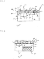
- FIG. 1 depicts a representative submodule 20 corresponding to a logic block.
- Submodule 20 includes representative electronic components 22 and 24, _such as semiconductor die or “chips” or passive components which have representative component connection pads 26, 28, 30 and 32 on the top or active major surfaces 34 and 36 thereof.
- Components 22 and 24 are supported on a submodule substrate 38, which may be a ceramic substrate with cavities milled therein with components 22 and 24 attached by glue as in the originally-disclosed HDI technology or, preferably, a molded substrate 38 such as is disclosed in Fillion et al U.S. Pat. Nos. 5,353,195 , 5,353,498 and 5,497,033 .
- Interconnecting component connection pads 26, 28, 30 and 32 is a first interconnect structure 50, which in FIG. 1 is a multilayer interconnect structure 50, overlying components 22 and 24 as well as substrate 38, and bonded thereto by means of an adhesive layer 52.
- Multilayer interconnect structure 50 in this example includes three patterned metallization layers and may, for example, be fabricated employing previously disclosed HDI fabrication techniques summarized above.
- multilayer interconnect structure 50 comprises a prefabricated flexible interconnect structure 53 including a first dielectric film layer 54 that is pre-patterned with metallization 56 and 58 on a connection-facing surface 60 and on a substrate-facing surface 62 respectively, as is disclosed in Cole et al U.S. Pat. No. 5,527,741 , and as summarized hereinabove in the context of the COF process.
- a representative via 64 interconnects portions of metallization planes 56 and 58.
- pre-patterned dielectric film layer 54 to provide two metallization planes is less e pensive than fabricating two thin film interconnect layers as in-the originally-disclosed HDI fabrication process.
- first dielectric cap layer 70 Overlying connection-facing surface 60 and patterned metallization 56 thereon is a first dielectric cap layer 70 which acts as an electrical insulation layer between top metallization plane 56 and subsequently added patterned metallization layer 74 and connection pads 76.
- Dielectric cap layer 70 may either be included as part of prefabricated flexible interconnect structure 53, or be added later.
- a first plurality of vias 72, formed by adaptive laser ablation extends through dielectric cap layer 70, and through at least portions of first dielectric film layer 54 in alignment with respective ones of component connection pads 26, 28, 30 and 32, as well as with predetermined portions of at least one of the patterned metallization planes 56 and 58.
- a patterned metallization layer 74 is formed on dielectric cap layer 70 and within vias 72 to complete the interconnection structure.
- metallization 74 includes submodule connection pads 76 on first dielectric cap layer 70, and preferably test pads comparable to pads 76 to facilitate functional and performance testing of submodule 20. Patterned metallization layer 74, with submodule connection pads 76 and first dielectric cap layer 70 together define an upper surface 78 of submodule 20.
- Multilayer interconnect structure 50 thus provides all of the internal connections within submodule 20, and provides connection pads 76 for all external block connections as well as test pads.
- external connection pads 76 are typically 5 to 10 mils (0.127 to 0.254 mm) square, larger than ⁇ component connection pads 26, 28, 30 and 32 which typically are 2 to 40 mils (0.0508 to 0.1016 mm) square.
- interconnect structure 50 is depicted in FIG. 1 as a multilayer interconnect structure 50, simpler interconnect structures may be employed.
- a single layer (i.e. single conductive layer) interconnect structure may be employed, including pre-patterned metallization 58 on substrate-facing surface 62, but omitting pre-patterned metallization 56 on connection-facing surface 60, as well as omitting dielectric cap layer 70.
- vias 72 are formed through dielectric film layer 54, and patterned metallization layer 74, including submodule connection pads 76, is formed directly on dielectric film layer 54.
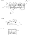
- FIG. 2 illustrates a similar submodule 21, with corresponding elements designated by identical reference numerals.
- Submodule 21 of FIG. 2 additionally includes an integral heat sink 80 for component 24, thermally connected by means of thermally conductive bonding material 82.
- substrate 38 comprise hardened substrate molding material, formed as summarized above and as disclosed in Fillion et al U.S. Pat. Nos. 5,353, 195 , 5,353,498 and 5,497,033 , by bonding top surfaces 34 and 36 of components 22 and 24 to prefabricated flexible interconnect structure 53, with component connection pads 26, 28, 30 and 32 thus facing interconnect structure 53, and then encapsulating the remaining surfaces of components 22 and 24 in a thermoset polymer molding compound, such as epoxy with low CTE particles mixed within it.
- a thermoset polymer molding compound such as epoxy with low CTE particles mixed within it.
- CMOS devices In other situations it is advantageous to employ a prefabricated substrate. This is of particular value in the case of components 22 and 24 that have electrical contacts on the back side that need to be accessed. Examples are some CMOS devices, GaAs RF devices, and power devices such as IGBTs, MOSFETs and MCTs.
- a preformed substrate 90 or body 90 has a substrate surface 92 and a cavity 94 with a depth corresponding to the thickness of representative components 96 and 98.
- Components 96 and 98 have respective back side electrical contacts 100 and 102, in addition to component connection pads 26, 28, 30 and 32 on top surfaces 34 and 36.
- Preformed substrate 90 is of the type previously employed in HDI structures and may comprise milled ceramic, milled metal, premolded metal, or a, preformed plastic or composite structure, as examples.
- Preformed substrate 90 preferably includes an electrically conductive layer 104 extending from the bottom of cavity 94 to substrate surface 92.
- Electrically conductive layer 94 may comprise a metal such as copper.
- components 96 and 98 are placed within cavity 94, and adhered employing electrically conductive material 106 such as solder or a polymer adhesive loaded with conductive particles to electrically connect back side electrical contacts 100 and 102 to electrically conductive layer 104.
- Interconnect structure 110 is then formed over component top surfaces 34 and 36 and over substrate surface 92, such as a multilayer interconnect structure 110.
- Interconnect structure 110 may either employ a prefabricated (pre-patterned) flexible Interconnect structure, or be fabricated and patterned layer-by-layer employing prev1ously-disclosed HDI fabrication techniques.
- a vja 1 12 is formed in alignment with electrically conductive layer 104 on substrate surface 92, terminating in a submodule connection pad 114.
- component back side electrical contacts 100 and 102 are electrically brought to connection pad 114 on the upper surface of the FIG. 3 submodule 88.
- FIG. 4 is a sectional side view and FIG. 5 is a plan view of a submodule 120 comprising a single component 122 with component connection pads 124, and no substrate.
- a simple interconnect structure 126 includes a flexible dielectric film layer 128 adhered to top surface 130 of component 122. Vias 132 are formed through dielectric film layer 128 in alignment with component connection pads 124. Patterned metallization 1.34. which includes submodule connection pads 136, extends through vias 132 in electrical contact with component connection pads 124.
- Representative submodules 20 ( FIG. 1 ), 21 ( FIG. 2 ), 88 ( FIG. 3 ) and 120 ( FIG. 4 ), corresponding to logic blocks of the circuit being implemented, are subsequently treated and handled as large chip components, having connection pads 76 or 136.
- Submodules 20, 21, 88 and 120 can be tested, and optionally burned in, and discarded if not functioning or not within specified design requirements.
- a second level design interconnects the submodules (building blocks) to create the full complex circuit, essentially using the same process and process alternatives, this time treating each submodule as a component.
- a second interconnect structure 186 comprises a prefabricated interconnect structure 188 including a dielectric film layer 190, comparable to first dielectric film layer 54, and comprising KAPTON® polyimide typically 10 to 100 microns in thickness.
- Dielectric film layer 190 has a connection-facing surface 192 and a submodule-facing surface 194, with respective patterned metallization planes 196 and 198 thereon. Openings 199 in metallization layers 196 and 198 correspond to the locations of submodule connection pads 76 in the final assembly. Accordingly, for the embodiments of FIGs.
- submodule connection pads 76 are not in direct electrical contact with patterned metallization plane 98 on submodule-facing surface 194 at the time of assembly and vias are subsequently formed to access submodule interconnection pads.
- the prefabricated structure of FIG. 6 includes representative vias 200 interconnecting selected portions of metallization planes 196 and 198.
- a dielectric cap layer 202 is provided over connection-facing surface 192 as well as over patterned metallization plane 196 thereon.
- Dielectric cap layer 202 may either be part of a prefabricated flexible interconnect structure, or be added later.
- dielectric layer 204 may be provided on submodule-facing surface 194, to protect patterned metallization plane 198.
- a layer 206 of adhesive is applied over dielectric layer 204 and over submodule-facing surface 194. It will be appreciated that optionally adhesive layer 206 may be applied to the upper surfaces of the FIG. 1 and FIG. 2 submodules 20 and 21.
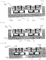
- FIG. 7 depicts a final assembly step and FIG. 8 depicts a complex multi-component module 208, where the FIG. 6 interconnect structure 186 is adhered to the FIG. 1 and the FIG. 2 submodules 20 and 21.
- Vias 210 are formed through second dielectric cap layer 202 and through at least portions of second dielectric film layer 190 in alignment with respective ones of submodule connection pads 176 and predetermined portions of at least one of the patterned metallization planes 196 and 198.
- Patterned metallization 212 portions of which extend within vias 210, completes interconnect structure 186, thus providing interconnections between all of individual submodules 20 and 21, as well as providing external connections for the completed structure 208.
- a prefabricated interconnect structure includes contact pads on the submodule-facing surface, which align with selected ones of the submodule connection pads.
- the contact pads are electrically connected with solder, conductive adhesive, or with an anisotrophically conductive adhesive.
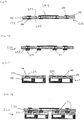
- FIGS. 9-12 depict an alternative method of final assembly, which utilizes solder to assemble submodules 220 and 221 to an interconnect structure 286.
- FIG. 9 depicts a multilayer interconnect structure 286, formed on a flexible polymer film 290 having a connection-facing surface 292 and a submodule-facing surface 294 with bottom side passivation 295.
- Top contact pads 296 as well as top interconnect traces 297 are formed on connection-facing surface 292, and bottom contact pads 298 are formed on submodule-facing surface 294.
- Vias 300 extend through polymer film 290.
- Contact pads 298 have a solderable metallurgy such as Ni/Au over Cu/Ti.
- FIG. 10 depicts the interconnect structure 286 of FIG. 9 with solder paste 310 or electrically conductive adhesive 31 dispensed onto contact pads 298.
- solder 310 can be plated directly onto contact pads 298.
- a common connector material solder or adhesive
- FIG. 11 depicts two submodules 220 and 221 with submodule connection pads 240 that align to respective bottom contact pads 298 and dispensed solder paste 310 on interconnect structure 286.
- Submodules 220 and 221 also have a patterned solder masks 230 with openings 232 to expose connection pads 240.
- FIG. 12 depicts a completed multi-module assembly 320 following mounting of the submodules 220 and 221 onto interconnect structure 286 and reflowing of solder paste 310 to electrically connect 220 and 221 submodules to interconnect structure 286.
- solder 310 is replaced by electrically conductive adhesive 311.
- Contact pads 298 on the interconnect structure 286 and connection pads 240 on submodules 220 and 221 have a pad metallurgy compatible with conductive adhesive 312.
- the conductive adhesive (instead of solder 310) is dispensed onto the contact pads 286 of interconnect structure 286.
- a thermal cure cycle is employed to mechanically and electrically bond submodules 220 and 221 to interconnect structure 286.
- FIGS. 13-17 depict another alternative assembly process in which an anisotropically conductive adhesive 312 is used to electrically and mechanically bond submodules 220 and 221 to interconnect structure 286.
- FIG. 13 depicts a multilayer interconnect structure 286 formed on a flexible polymer film 290 having a connection-facing surface 292 and a submodule-facing surface 294, with bottom side passivation 295.
- Top contact pads. 296 as well as top interconnect traces 297 are formed on connection-facing surface 292.
- Bottom contact pads 298 as well as bottom side interconnect trace 299 are formed on submodule-facing surface 294.
- Contact pads 298 have a metallurgy compatible with conductive adhesive such as Ni/Au over Cu/Ti:
- FIG. 14 depicts the interconnect structure 286 of FIG. 13 with a uniform layer of anisotropically conductive adhesive 312 dispensed over submodule-facing surface 294.
- Anisotripically conductive ⁇ adhesives can be used to make electrical connections in the Z plane without making electrical connections in the X and Y planes.
- the thickness preferably ranges from about 6 microns to about 250 microns.
- the material may comprise any appropriate anisotropically adhesive material.
- One such material for example, is available from 3M company as a thermoset-thermoplastic blend filled with nickel coated polymer and sold under the order number 5305R.
- FIG. 15 depicts two submodules 220 and 221 with connection pads 240 that align to respective bottom contact pads 298 on interconnect structure 286.
- Submodules 220 and 221 also have patterned solder masks 230 with openings 232 to expose the connection pads 240.
- the solder mask is useful for preventing undesired short circuits in the event that metalization on the interconnect structure overlaps metalization on the submodules in locations where connections are not desired.
- FIG. 16 depicts the two submodules 220 and 221 mounted onto the interconnect structure 286 prior to curing of anisotropically conductive adhesive 312.
- FIG. 17 depicts the completed multi-module assembly 340 containing submodules 220 and 221 mounted onto interconnect structure 286 following curing of anisotropically conductive adhesive 312 to electrically and mechanically connect submodules 220 and 221 interconnect structure 286.
- Curing can be performed as instructed by the material manufacturer. In one embodiment, curing is performed for about two to five minutes at a temperature ranging from about 160 °C to about 180 °C.
- FIG. 18 is an enlarged and expanded cross-sectional view of contact pad 298 on interconnect structure 286 and submodule connection pad 240 on submodule _220 after mounting submodule 220 to interconnect structure 286 and prior to the curing of anisotropically conductive adhesive 312.
- representative electrically conductive particles 314 and 316 within anisotropically conductive adhesive 312 are not making electrical connection between contact pad 298 and submodule connection pad 240.
- FIG. 19 depicts the same structure as FIG. 18 , however following curing of anisotropically conductive adhesive 312.
- Representative electrically conductive particles 316 are in physical contact with both interconnect structure 286 contact pad 298 as well as submodule 220 submodule connection pad 240 thereby providing electrical connection between pads 298 and 240.
- Representative electrically conductive particle 314 does not make any electrical connection.
- submodules 20 and 21 of FIG. 8 can be encapsulated.
- FIG. 20 depicts the formation of a plastic molded substrate structure 350 that encapsulates submodules 22 and 21 and the exposed areas of the back side of interconnect structure 186 of the FIG. 8 complex multi-component module 208.
- FIGS. 21-23 depict the mounting of the complex multi-component module 208 of FIG. 8 into the cavity 360 of an electronic component package 370 or enclosure 370.
- FIG. 21 shows the multi-component module 208 and electronic component package 370 with a polymeric adhesive 372 dispensed on portions of the top surface 374 of the package base 376.
- the component package is shown with a cavity 360, the cavity is optional.
- the component package may comprise a plate without a cavity.
- FIG. 22 depicts the multi-component module 208 mounted onto polymeric adhesive 372 on the top surface of package base 376 in electronic component package 370 after curing of adhesive 372.
- FIG. 23 depicts an optional step of partially encapsulating the multi-component module 208 within package 370, employing an encapsulant 380, which comprises a substrate molding material.
- a defective die results in only one submodule building block being scrapped, rather than an entire complex multi-component module.
- the previous monolithic MCM approach would have a 19% module yield loss, while the hierarchical structure of the invention would have no final yield loss (due to die loss), and only 5% module yield loss.
- the pre-patterned dielectric interconnect structure has excellent interconnect and assembly yield (module yield loss not associated with die yield) very complex modules will have some associated interconnect and/or assembly yield losses.
- the hierarchical submodule structure of the invention reduces these losses in the same way that module yield loss is due to die yield losses are reduced.
- the previously-disclosed COF structure can offer two layers of interconnect in the prefabricated dielectric film because of tolerance limits of aligning more than one prefabricated dielectric film to another, and the fact that prefabricated dielectric film with more than two interconnect layers is too thick for current COF processing techniques.
- the use of building block submodules, fabricated with double sided prefabricated dielectric interconnect layer during supermodule assembly provides six layers of interconnection, for prefabricated flexible dielectric film layers and two thin film interconnect layers.
Abstract
A circuit design is logically partitioned into a plurality of blocks. As a first hierarchial assembly level, the blocks are fabricated as individual submodules (20, 21) each including at least one electronic component (22, 24) with component connection pads (26, 28, 30, 32) on a top surface (34, 36), and a first interconnect structure (50) including at least one interconnect layer (56, 58) bonded to the top surfaces (34, 36), and interconnecting selected ones of the component connection pads (26, 28, 30, 32). Submodule connection pads (76) are provided on upper surfaces (78) of the submodules (20, 21). As a second hierarchial assembly level, a second interconnect structure (186) is bonded to the upper surfaces (78) and interconnects selected ones of the submodule connection pads (76).
Description
- This invention relates generally to complex multichip modules (MCMs) and, more particularly, to complex MCMs which can cost-effectively be assembled with high yields, as well as to corresponding methods of manufacture.
- As disclosed in
Eichelberger et al U.S. Pat. No. 4,783,695 , and subsequent related patents, some of which are referred to herein below, high density interconnect (HDI) technology has quite successfully been employed to interconnect large numbers of complex semiconductor devices to make multichip modules, with improved electrical, thermal, and mechanical performance characteristics, compared to various other single chip and multichip packaging approaches. Very briefly, HDI MCMs include a plurality of semiconductor integrated circuit chips and other electronic components - mounted on a substrate. The chips and other electronic components are interconnected by a multilayer interconnect structure including interleaved layers of thin film polymer dielectric material (e.g. KAPTON polyimide- KAPTON is a trademark of Dupont Co.) and patterned metallization, with vias formed in the polymer layers. - A broad spectrum of modules have been successfully fabricated using this HDI technology. These include high chip count modules (including 40 to 50 chips), high pin count modules (with 400 1/0 lines), high speed digital modules (200 MHz on Si, and 2 Ghz on GaAs), mixed analog and digital modules (e.g. 44 channel PJD conversion modules),. power conversion modules (e.g. 50V to 5V DC to DC), microwave modules (S, C, Ku and X-band) and millimeter wave modules (44 Ghz).
- More particularly, the previously-disclosed HDI structure employs a ceramic substrate, made of alumina, for example, with a thickness between 25 and 100 mils. The substrate is of appropriate size and strength for the overall electronic system in which it is utilized. This size is typically on the order of two inches square.
- Individual cavities, or one large cavity, having appropriate depths at the intended locations of the various chips, are prepared. This may be done by starting with a bare substrate having a uniform thickness and the desired size. Conventional, laser or ultrasonic milling is used to form the cavities in which the various chips and other components are subsequently positioned. For systems where it is desired to place chips of uniform size edge-to-edge, a single large cavity may be satisfactory.
- The various components are placed in their desired locations within the cavities and adhered by means of a thermoplastic adhesive layer, preferably ULTEM® polyetherimid resin (ULTEM is a trademark of General Electric Co.). More particularly, the entire structure is heated to the softening point of the ULTEM polyetherimide (in the vicinity of 217°C to 235°C depending on the formulation used) and then cooled to thermoplastically bond the individual components to the substrate. At this stage, the upper surfaces of all components and the substrate are disposed in a substantially common plane.
- The multilayer interconnect overcoat structure is then built up to electrically interconnect the components into an actual functioning system. To begin the HDI overcoat structure, a polyimide dielectric film, which may be KAPTON® polyimide, about 0.0005 to 0.003 inch (12.5 to 75 microns) thick is pretreated to promote adhesion and coated on one side with ULTEM polyetherimide resin or another thermoplastic and laminated across the top of the chips, other components and the substrate, with the ULTEM resin serving as a thermoplastic adhesive to hold the KAPTON film in place.
- The actual as-placed locat1ons of the various components and contact pads thereon are determined. and v1a holes are adaptively laser drilled in the KAPTON film and ULTEM adhesive layers in alignment with the contact pads on the electronic components. Exemplary laser drilling techniques are disclosed in
Eichelberger et al U.S. Pat. Nos. 4,714,516 and4,894, 115 ; and in Loughran et alU.S. Pat. No. 4,764,485 . - A metallization layer is deposited over the KAPTON film layer and extends into the via holes to make electrical contact to the contact pads disposed thereunder. This metallization layer may be patterned to form individual conductors during the process of depositing it, or may be deposited as a continuous layer and then patterned using photoresist and etching. The photoresist is preferably exposed using a laser which is scanned relative to the substrate to provide an accurately aligned conductor pattern at the end of the process. Exemplary techniques for patterning the metallization layer are disclosed in Wojnarowski et al
U.S. Pat. Nos. 4,780,177 and4,842,677 and in Eichelberger et alU.S. Pat. No. 4,835,704 which discloses an ••Adaptive Lithography System to Provide High Density Interconnect. Any misposition of the individual electric components and their contact pads can be compensated for by and adaptive· laser lithography system as disclosed inU.S. Pat. No. 4,835,704 . - Additional dielectric and metallization layers are provided as required in order to make all of the desired electrical connections among the chips.
- Yield and cost considerations have been important factors in the fabrication of such HDI modules. Thus, due in part to the varying die yields of the individual semiconductor die, initial module yields following initial assembly, which may be viewed as the first pass, range from 25% to 90%. With the implementation of module rework and repair, final module yields were improved to 80% to 100%.
- An HDI module can be disassembled for repair or replacement of a faulty component and then reassembled without significant risk to the good components incorporated within the system. Repairability is particularly important where fifty or more chips having a cost of as much as $2,000.00, each, may be incorporated in a single system on one substrate. Techniques for testing and repairing HDI MCMs are disclosed in Eichelberger et al
U.S. Pat. Nos. 4,878,991 ,4,884,112 and4,937,203 ; and inWojnarowski et al U.S. Pat. No. 5,154,793 . - One key element to the repair of a failing HDI MCM as disclosed in those patents is that the adhesive which attaches the first layer of the overlay to the components, and the adhesive which attaches the components to the substrate, are both thermoplastic polymers that soften and release when expos d to an elevated temperature. Another key to the disclosed rework process is that the adhesive which attaches the overlay softens at a lower temperature than the adhesive which attaches the die or other components. Thus,. by raising a defective module to a temperature above the overlay adhesive softening temperature, but below the die attach adhesive softening temperature, the overlay structure can be removed from the substrate without disturbing the chips below. To subsequently remove a chip, localized heat is applied to the selected chip raising the temperature of the chip above the softening temperature of the die attach adhesive, and. permitting chip removal by a number of manual methods.
- The module is then repaired by adhesive clean up, reapplication of a die adhesive, placement of the replacement die and curing of the die attach adhesive. This is followed by repeating all the overlay thin film processing steps.
- A subsequent technology, known as COF (Chip On Flex) was developed to reduce the complexity and cost of the HDI process, in two respects.
- In overview, a first aspect of the COF technology, as disclosed in
Fillion et al U.S. Pat. Nos. 5,353,498 and5,497,033 , is that the HDI ceramic substrate milling process is eliminated by employing a molding process. Thus, the die top surfaces (which support component connection pads) are bonded to a polymer stretched film, employing a thermoplastic or thermoset adhesive, and then a polymeric molding material, such as an epoxy-based molding compound, is employed to encapsulate all remaining surfaces of the chips and other electronic components. The chips and other electronic components are thus encapsulated within a body of hardened epoxy-based molding compound, which forms the substrate. - In overview, a second aspect of the COF technology, as discussed in
Fillion et al U.S. Pat. No. 5,353,195 with respect to power and ground connections and inCole et al U.S. Pat. No. 5,527,741 with respect to signal connections, is that a polymer dielectric stretched film which is pre-patterned on either or both sides is used to provide two interconnect layers that do not require the relatively expensive HDI thin film processing steps summarized hereinabove. - The overlay structure is then completed employing the previously-disclosed HDI thin film processing techniques, using a laser to form via holes, and forming a third patterned metallization layer, including connections through the vias to the component connection pads.
- More particularly, as the COF process is generally implemented, a polymer film structure comprises a polyimide film of uniform · thickness, which may be within the range of 10 to 100 microns, having a pattern of metallization on the top surface, bottom surface, or both surfaces. Typical metallization thickness is within the range of 1 to 200 microns, and the metallization comprises Cu or Al, and a barrier layer metal such as Ti or Cr. A polymer adhesive is coated over either selected areas of or the entire surface of the bottom side of the polymer film structure. The polymer adhesive may be a thermoset or a thermoplastic material.
- At least one component is mounted to the bottom side of the polymer film structure, with a top (active) surface of the component (or components) in contact with the polymer adhesive and mechanically bonded to the polymer film structure by the adhesive. The component is then encapsulated along its bottom and side surfaces within a body of plastic molding compound that also covers at least a portion of the adhesive-coated bottom side of the polymer film structure. The molding compound is a thermoset polymer, such as a epoxy with low CTE (coefficient of thermal expansion) particles mixed within it.
- Vias are then formed through the polymer film, aligned with respective component contact pads on the top surface of the component. In addition, at least one via extends through the polymer film to the metallization on the bottom surface of the polymer film structure. Vias may be formed by laser ablation, plasma etching, chemical etching, mechanical milling, or by a combination of these methods. Finally, an upper metallization layer is formed and patterned, extending through the vias to electrically contact the component contact pads and the metallization on the bottom surface of the polymer film structure, and to leave contact pads on the top surface.
- The resultant structure can have three layers of interconnection, but advantageously only one of these layers requires the HDI thin film processing steps at the time of assembly. A disadvantage however is that the encapsulated molding step makes reworking or repair of a COF module that happen to have a defective die difficult and costly, or even impossible.
- The COF technology accordingly is particularly applicable.to simple high-yielding few-chip modules. The COF technology, despite its cost advantages, is not as useful with more complex MCMs in view of yield issues.
- It is therefore seen to be desirable to cost effectively fabricate complex MCMs with high-yield, and to employ COF technology in the fabrication of complex MCMs.
- In an exemplary embodiment of the invention, a plurality of MCM building block submodules (or one or more MCM building block submodules, and one or more single chip components) are assembled into a more complex module, after individually testing the building block submodules. A method of fabricating a complex multi-component module begins with the step of logically partitioning a circuit design into a plurality of blocks. Each block includes at least one electronic component.
- As a first hierarchial assembly level, the blocks are fabricated as individual submodules. Each submodule includes at least one electronic component with component connection pads thereon, and which may be supported on a submodule substrate. A first interconnect structure is provided overlying and bonded to the electronic components, interconnecting selected ones of the component connection pads. The first interconnect structure may.be a multilayer interconnect structure including interleaved layers of dielectric material and con9uctive material. Submodule connection pads are included on an upper surface of the first interconnect structure.
- As a second hierarchial assembly level, the submodules are interconnected in much ·the same manner as the individual components during the first assembly level. Thus a second interconnect structure is provided overlying and bonded to the upper surfaces of the submodules, interconnecting selected ones of the submodule connection pads. The second interconnect structure likewise may be a multilayer interconnect structure including interleaved layers of dielectric material and conductive material such as metallization.
- Embodiments of the invention will now be described, by way of example, with reference to the accompanying drawings, in which:
-
FIG. 1 is a sectional side view of a representative submodule including two representative electronic components supported on a substrate and interconnected by a first multilayer Interconnect structure corresponding to a first level of assembly; -
FIG. 2 is a sectional side view of another representative submodule including two representative electronic components supported on a substrate and interconnected by a first multilayer interconnect structure corresponding to a first level of assembly; -
FIG. 3 is a sectional side view of a submodule employing a prefabricated substrate; -
FIG. 4 is a sectional side view andFIG. 5 is a plan view of a submodule in the form of a single-chip COF package; -
FIG. 6 is a sectional side view of a second dielectric film layer and related structure used- to fabricate a second multilayer interconnect structure; -
FIG. 7 depicts the assembly of theFIG. 6 dielectric film layer and theFIG. 1 and FIG. 2 submodules; -
FIG. 8 depicts the final structure after the formation of vias and patterned metallization; -
FIGS. 9 through 12 depict a process flow for the second hierarchial assembly level, using solder or an electrically conductive adhesive; -
FIGS. 13 through 17 depict a process flow for the second hierarchial assembly level, using anisotropically conductive adhesive; -
FIGS. 18 and 19 are enlarged and expanded cross-sectional- views of an electrical connection using anisotropically conductive adhesive before and after curing of the adhesive; -
FIG. 20 depicts the formation of a plastic molded substrate on the multi-module assembly ofFIG. 8 ; and -
FIGS. 21-23 depict the mounting of the multi-module assembly ofFIG. 8 into a cavity formed in an electronic component package or enclosure. - The invention is particularly applicable to the fabrication of 2 complex multichip modules employing a modification of the previously-disclosed HDI process briefly discussed hereinabove. The invention may be embodied in MCMs including many individual semiconductor chips and fabricated with high yield.
- As a preliminary design step, a complex circuit with a large number of complex semiconductor components and passive support components is divided into a number of logic blocks. Each logic block contains one or more components, typically from two to ten or more components per logic block. The partitioning of the circuit into logic blocks is based on a number of factors including, but not limited to the number of interconnections within a logic block, the number of connections external to each logic block, the complexity and 1/0 count of each of the components included in a logic block, the estimated yield loss of each component, the power dissipation of each component, and the function and other characteristics of each component', for example, logic vs. RAM, signal vs. logic, high power vs. low power, and digital vs. RF.
-
FIG. 1 depicts arepresentative submodule 20 corresponding to a logic block.Submodule 20 includes representativeelectronic components component connection pads major surfaces -
Components submodule substrate 38, which may be a ceramic substrate with cavities milled therein withcomponents substrate 38 such as is disclosed inFillion et al U.S. Pat. Nos. 5,353,195 ,5,353,498 and5,497,033 . - Interconnecting
component connection pads first interconnect structure 50, which inFIG. 1 is amultilayer interconnect structure 50, overlyingcomponents substrate 38, and bonded thereto by means of anadhesive layer 52. -
Multilayer interconnect structure 50 in this example includes three patterned metallization layers and may, for example, be fabricated employing previously disclosed HDI fabrication techniques summarized above. - Preferably however,
multilayer interconnect structure 50 comprises a prefabricated flexible interconnect structure 53 including a firstdielectric film layer 54 that is pre-patterned withmetallization 56 and 58 on a connection-facing surface 60 and on a substrate-facingsurface 62 respectively, as is disclosed inCole et al U.S. Pat. No. 5,527,741 , and as summarized hereinabove in the context of the COF process. There are openings 63 in metallization layers 56 and 58 corresponding tocomponent connection pads component connection pads surface 62 at the time of assembly, and vias are subsequently formed to accesscomponent interconnection pads metallization planes 56 and 58. - The use of pre-patterned
dielectric film layer 54 to provide two metallization planes is less e pensive than fabricating two thin film interconnect layers as in-the originally-disclosed HDI fabrication process. - Overlying connection-facing surface 60 and patterned
metallization 56 thereon is a first dielectric cap layer 70 which acts as an electrical insulation layer betweentop metallization plane 56 and subsequently added patterned metallization layer 74 andconnection pads 76. Dielectric cap layer 70 may either be included as part of prefabricated flexible interconnect structure 53, or be added later. A first plurality ofvias 72, formed by adaptive laser ablation extends through dielectric cap layer 70, and through at least portions of firstdielectric film layer 54 in alignment with respective ones ofcomponent connection pads vias 72 to complete the interconnection structure. In addition, metallization 74 includessubmodule connection pads 76 on first dielectric cap layer 70, and preferably test pads comparable topads 76 to facilitate functional and performance testing ofsubmodule 20. Patterned metallization layer 74, withsubmodule connection pads 76 and first dielectric cap layer 70 together define anupper surface 78 ofsubmodule 20. -
Multilayer interconnect structure 50 thus provides all of the internal connections withinsubmodule 20, and providesconnection pads 76 for all external block connections as well as test pads. To facilitate subsequent interconnect- processing,external connection pads 76 are typically 5 to 10 mils (0.127 to 0.254 mm) square, larger than·component connection pads - Even though
interconnect structure 50 is depicted inFIG. 1 as amultilayer interconnect structure 50, simpler interconnect structures may be employed. For example, a single layer (i.e. single conductive layer) interconnect structure may be employed, including pre-patterned metallization 58 on substrate-facingsurface 62, but omittingpre-patterned metallization 56 on connection-facing surface 60, as well as omitting dielectric cap layer 70. In this example, vias 72 are formed throughdielectric film layer 54, and patterned metallization layer 74, includingsubmodule connection pads 76, is formed directly ondielectric film layer 54. -
FIG. 2 illustrates asimilar submodule 21, with corresponding elements designated by identical reference numerals. -
Submodule 21 ofFIG. 2 additionally includes anintegral heat sink 80 forcomponent 24, thermally connected by means of thermally conductive bonding material 82. - In many situations it is preferable that
substrate 38 comprise hardened substrate molding material, formed as summarized above and as disclosed inFillion et al U.S. Pat. Nos. 5,353, 195 ,5,353,498 and5,497,033 , by bondingtop surfaces components component connection pads components - However, in other situations it is advantageous to employ a prefabricated substrate. This is of particular value in the case of
components - Thus, and referring to
submodule 88 ofFIG. 3 , a preformedsubstrate 90 orbody 90 has a substrate surface 92 and acavity 94 with a depth corresponding to the thickness ofrepresentative components Components electrical contacts component connection pads top surfaces Preformed substrate 90 is of the type previously employed in HDI structures and may comprise milled ceramic, milled metal, premolded metal, or a, preformed plastic or composite structure, as examples. -
Preformed substrate 90 preferably includes an electricallyconductive layer 104 extending from the bottom ofcavity 94 to substrate surface 92. Electricallyconductive layer 94 may comprise a metal such as copper. During the fabrication process,components cavity 94, and adhered employing electricallyconductive material 106 such as solder or a polymer adhesive loaded with conductive particles to electrically connect back sideelectrical contacts conductive layer 104. - An
interconnect structure 110 is then formed over component top surfaces 34 and 36 and over substrate surface 92, such as amultilayer interconnect structure 110.Interconnect structure 110 may either employ a prefabricated (pre-patterned) flexible Interconnect structure, or be fabricated and patterned layer-by-layer employing prev1ously-disclosed HDI fabrication techniques. In addition tovias 72 making electrical connection tocomponent connection pads vja 1 12 is formed in alignment with electricallyconductive layer 104 on substrate surface 92, terminating in asubmodule connection pad 114. Thus, component back sideelectrical contacts connection pad 114 on the upper surface of theFIG. 3 submodule 88. - As another alternative,
FIG. 4 is a sectional side view andFIG. 5 is a plan view of asubmodule 120 comprising asingle component 122 withcomponent connection pads 124, and no substrate. Asimple interconnect structure 126 includes a flexibledielectric film layer 128 adhered totop surface 130 ofcomponent 122.Vias 132 are formed throughdielectric film layer 128 in alignment withcomponent connection pads 124. Patterned metallization 1.34. which includessubmodule connection pads 136, extends throughvias 132 in electrical contact withcomponent connection pads 124. - Representative submodules 20 (
FIG. 1 ), 21 (FIG. 2 ), 88 (FIG. 3 ) and 120 (FIG. 4 ), corresponding to logic blocks of the circuit being implemented, are subsequently treated and handled as large chip components, havingconnection pads Submodules - A second level design interconnects the submodules (building blocks) to create the full complex circuit, essentially using the same process and process alternatives, this time treating each submodule as a component.
- Thus, and with reference to
FIG. 6 , asecond interconnect structure 186 comprises aprefabricated interconnect structure 188 including adielectric film layer 190, comparable to firstdielectric film layer 54, and comprising KAPTON® polyimide typically 10 to 100 microns in thickness.Dielectric film layer 190 has a connection-facingsurface 192 and a submodule-facingsurface 194, with respectivepatterned metallization planes Openings 199 inmetallization layers submodule connection pads 76 in the final assembly. Accordingly, for the embodiments ofFIGs. 6-8 ,submodule connection pads 76 are not in direct electrical contact with patternedmetallization plane 98 on submodule-facingsurface 194 at the time of assembly and vias are subsequently formed to access submodule interconnection pads. The prefabricated structure ofFIG. 6 includesrepresentative vias 200 interconnecting selected portions ofmetallization planes - A
dielectric cap layer 202, is provided over connection-facingsurface 192 as well as over patternedmetallization plane 196 thereon.Dielectric cap layer 202 may either be part of a prefabricated flexible interconnect structure, or be added later. - Similarly, another
dielectric layer 204 may be provided on submodule-facingsurface 194, to protect patternedmetallization plane 198. Finally, alayer 206 of adhesive is applied overdielectric layer 204 and over submodule-facingsurface 194. It will be appreciated that optionallyadhesive layer 206 may be applied to the upper surfaces of theFIG. 1 and FIG. 2 submodules -
FIG. 7 depicts a final assembly step andFIG. 8 depicts a complexmulti-component module 208, where theFIG. 6 interconnect structure 186 is adhered to theFIG. 1 and theFIG. 2 submodules dielectric cap layer 202 and through at least portions of seconddielectric film layer 190 in alignment with respective ones of submodule connection pads 176 and predetermined portions of at least one of the patternedmetallization planes interconnect structure 186, thus providing interconnections between all ofindividual submodules structure 208. - In alternative second hierarchial level assembly methods, a prefabricated interconnect structure includes contact pads on the submodule-facing surface, which align with selected ones of the submodule connection pads. The contact pads are electrically connected with solder, conductive adhesive, or with an anisotrophically conductive adhesive. Thus,
FIGS. 9-12 depict an alternative method of final assembly, which utilizes solder to assemblesubmodules interconnect structure 286. -
FIG. 9 depicts amultilayer interconnect structure 286, formed on aflexible polymer film 290 having a connection-facingsurface 292 and a submodule-facingsurface 294 withbottom side passivation 295.Top contact pads 296 as well as top interconnect traces 297 are formed on connection-facingsurface 292, andbottom contact pads 298 are formed on submodule-facingsurface 294.Vias 300 extend throughpolymer film 290. Contactpads 298 have a solderable metallurgy such as Ni/Au over Cu/Ti. -
FIG. 10 depicts theinterconnect structure 286 ofFIG. 9 withsolder paste 310 or electrically conductive adhesive 31 dispensed ontocontact pads 298. Alternatively,solder 310 can be plated directly ontocontact pads 298. In practice, a common connector material (solder or adhesive) will be used for each connection. - With respect to solder,
FIG. 11 depicts twosubmodules submodule connection pads 240 that align to respectivebottom contact pads 298 and dispensedsolder paste 310 oninterconnect structure 286.Submodules solder masks 230 withopenings 232 to exposeconnection pads 240. -
FIG. 12 depicts a completedmulti-module assembly 320 following mounting of thesubmodules interconnect structure 286 and reflowing ofsolder paste 310 to electrically connect 220 and 221 submodules to interconnectstructure 286. - With respect to the electrically conductive adhesive, in an alternative assembly process which also is depicted in the same
FIGS. 9-12 , thesolder 310 is replaced by electricallyconductive adhesive 311. Contactpads 298 on theinterconnect structure 286 andconnection pads 240 onsubmodules conductive adhesive 312. The conductive adhesive (instead of solder 310) is dispensed onto thecontact pads 286 ofinterconnect structure 286. A thermal cure cycle is employed to mechanically andelectrically bond submodules structure 286. -
FIGS. 13-17 depict another alternative assembly process in which an anisotropicallyconductive adhesive 312 is used to electrically and mechanically bond submodules 220 and 221 to interconnectstructure 286. -
FIG. 13 depicts amultilayer interconnect structure 286 formed on aflexible polymer film 290 having a connection-facingsurface 292 and a submodule-facingsurface 294, withbottom side passivation 295. Top contact pads. 296 as well as top interconnect traces 297 are formed on connection-facingsurface 292.Bottom contact pads 298 as well as bottomside interconnect trace 299 are formed on submodule-facingsurface 294. Contactpads 298 have a metallurgy compatible with conductive adhesive such as Ni/Au over Cu/Ti: -
FIG. 14 depicts theinterconnect structure 286 ofFIG. 13 with a uniform layer of anisotropically conductive adhesive 312 dispensed over submodule-facingsurface 294. Anisotripically conductive ·adhesives can be used to make electrical connections in the Z plane without making electrical connections in the X and Y planes. The thickness preferably ranges from about 6 microns to about 250 microns. The material may comprise any appropriate anisotropically adhesive material. One such material, for example, is available from 3M company as a thermoset-thermoplastic blend filled with nickel coated polymer and sold under the order number 5305R. -
FIG. 15 depicts twosubmodules connection pads 240 that align to respectivebottom contact pads 298 oninterconnect structure 286.Submodules solder masks 230 withopenings 232 to expose theconnection pads 240. The solder mask is useful for preventing undesired short circuits in the event that metalization on the interconnect structure overlaps metalization on the submodules in locations where connections are not desired. -
FIG. 16 depicts the twosubmodules interconnect structure 286 prior to curing of anisotropicallyconductive adhesive 312. -
FIG. 17 depicts the completedmulti-module assembly 340 containingsubmodules interconnect structure 286 following curing of anisotropically conductive adhesive 312 to electrically and mechanically connectsubmodules interconnect structure 286. Curing can be performed as instructed by the material manufacturer. In one embodiment, curing is performed for about two to five minutes at a temperature ranging from about 160 °C to about 180 °C. -
FIG. 18 is an enlarged and expanded cross-sectional view ofcontact pad 298 oninterconnect structure 286 andsubmodule connection pad 240 on submodule _220 after mountingsubmodule 220 tointerconnect structure 286 and prior to the curing of anisotropicallyconductive adhesive 312. InFIG. 18 , representative electricallyconductive particles contact pad 298 andsubmodule connection pad 240. -
FIG. 19 depicts the same structure asFIG. 18 , however following curing of anisotropicallyconductive adhesive 312. Representative electricallyconductive particles 316 are in physical contact with bothinterconnect structure 286contact pad 298 as well assubmodule 220submodule connection pad 240 thereby providing electrical connection betweenpads conductive particle 314 does not make any electrical connection. - Just as
individual components substrate mdlding material 38 as described hereinabove with referenceFIGS. 1 and 2 , or placed w1thin acavity 94 of a preformedsubstrate 90 as described hereinabove w1th reference toFIG. 3 , submodules 20 and 21 ofFIG. 8 (or submodules 220 and 221 ofFIGS. 12 and17 ) can be encapsulated. - In particular,
FIG. 20 depicts the formation of a plastic moldedsubstrate structure 350 that encapsulates submodules 22 and 21 and the exposed areas of the back side ofinterconnect structure 186 of theFIG. 8 complexmulti-component module 208. - Alternatively,
FIGS. 21-23 depict the mounting of the complexmulti-component module 208 ofFIG. 8 into thecavity 360 of anelectronic component package 370 orenclosure 370.FIG. 21 shows themulti-component module 208 andelectronic component package 370 with apolymeric adhesive 372 dispensed on portions of the top surface 374 of thepackage base 376. Although the component package is shown with acavity 360, the cavity is optional. For example, the component package may comprise a plate without a cavity. -
FIG. 22 depicts themulti-component module 208 mounted ontopolymeric adhesive 372 on the top surface ofpackage base 376 inelectronic component package 370 after curing ofadhesive 372. -
FIG. 23 depicts an optional step of partially encapsulating themulti-component module 208 withinpackage 370, employing anencapsulant 380, which comprises a substrate molding material. - The processes just described can be extended to a third hierarchical level of assembly, and even higher.
- It will appreciated that the hierarchical approach of the invention provides a number of benefits and advantages.
- One benefit is that a defective die results in only one submodule building block being scrapped, rather than an entire complex multi-component module. For example, in a design comprising four submodule building blocks with a 5% yield loss per block, the previous monolithic MCM approach would have a 19% module yield loss, while the hierarchical structure of the invention would have no final yield loss (due to die loss), and only 5% module yield loss.
- Although the pre-patterned dielectric interconnect structure has excellent interconnect and assembly yield (module yield loss not associated with die yield) very complex modules will have some associated interconnect and/or assembly yield losses. The hierarchical submodule structure of the invention reduces these losses in the same way that module yield loss is due to die yield losses are reduced.
- As a third advantage, the previously-disclosed COF structure can offer two layers of interconnect in the prefabricated dielectric film because of tolerance limits of aligning more than one prefabricated dielectric film to another, and the fact that prefabricated dielectric film with more than two interconnect layers is too thick for current COF processing techniques. The use of building block submodules, fabricated with double sided prefabricated dielectric interconnect layer during supermodule assembly provides six layers of interconnection, for prefabricated flexible dielectric film layers and two thin film interconnect layers.
Claims (20)
- A complex multi-component module (208) comprising:a plurality of submodules (20, 21), each submodule (20, 21) includingat least one electronic component (22, 24) including a top surface (34, 36) and component connection pads (26, 28, 30, 32) on the top 10 surface (34, 36), anda first interconnect structure (50) overlying and bonded to the top surface (34, 36) of the at least one electronic component (22, 24) and interconnecting selected ones of the component connection pads (26, 28, 30, 32), the first interconnect structure (50) including submodule connection pads (76) on an upper surface (78); anda second interconnect structure (186) overlying and bonded to the upper surfaces of the submodules (20, 21) and interconnecting selected ones of the submodule connection pads (76).
- The module of claim 1, wherein at least one submodule (20, 21) includes a submodule substrate (38) supporting the at least one electronic component (22, 24).
- The module of claim 2, wherein the submodule substrate (38) comprises hardened substrate molding material (38) surrounding the at least one electronic component (22, 24) except for the top surface (34, 36).
- The module of claim 2, wherein the submodule substrate comprises a preformed body (90) including a component cavity (94) receiving the at least one component (22, 24).
- The module of claim 1, wherein the first interconnect structure (50) comprises interleaved layers of dielectric material (54) and conductive material (56, 58).
- The module of claim 5, wherein the second interconnect structure (186) comprises interleaved layers of dielectric material (190) and conductive material (196, 198).
- The module of claim 1, wherein within each of the individual submodules (20, 21) the first interconnect structure (50) comprises:a dielectric film layer (54) having a connection-facing surface (60) and a substrate-facing surface (62), with the substrate-facing surface (62) having a patterned conductive material plane (58) thereon including plane openings (63) patterned on the substrate-facing surface (62);the dielectric film layer (54) being adhered to the at least one component (22, 24) with the component connection pads (26) located within the openings (63) in the patterned conductive material plane (58);a plurality of vias (72) extending through at least portions of the dielectric film layer (54) of the first interconnect structure (50), in alignment with respective ones of the component connection pads (26, 28, 30, 32) and in alignment with predetermined portions of the patterned conductive material plane (58) on the dielectric film layer (54) of the first interconnect structure (50); andpatterned conductive material on the dielectric film layer (54) of the first interconnect structure (50) extending through the vias (72) to interconnect selected ones of the component connection pads (26, 28, 30, 32) and selected portions of the patterned conductive material plane (58) on the dielectric film layer (54), .and to define the submodule connection pads (76).
- The module of claim 7, wherein at least one submodule (20, 21) includes a submodule substrate (38) supporting the at least one electronic component (22, 24) and comprising hardened substrate molding material (38) surrounding the at least one electronic component (22, 24) except for the top surface (34, 36).
- The module of claim 7, wherein at least one submodule (88) includes a submodule substrate (90) supporting the at least one electronic component (96, 98), the substrate (90) having a substrate surface (92) and at least one cavity (94) with a depth corresponding to the thickness of the at least one component (22, 24), the at least one component (22, 24) being adhered within the cavity (94) face up with the top surface of the component (22, 24) generally coplanar with the substrate surface (92).
- The module of claim 9, wherein:the substrate (90) includes an electrically conductive layer (104) extending from the bottom of the cavity (94) to the substrate surface (92);the at least one component (96, 98) includes a back side contact adhered to the electrically conductive layer (104) within the cavity by an electrically conductive material (106);the plurality of vias (72) includes at least one via (72) extending to and in alignment with the electrically conductive layer (104) on the substrate surface (92).
- The module of claim 1, wherein within each of the individual submodules (20, 21) the first interconnect structure (50) comprises:a dielectric film layer (54) having a connection-facing surface (60) and a substrate-facing surface (62), with each of the surfaces (60, 62) of the dielectric film layer (54) of the first interconnect structure (50) having a respective patterned conductive material plane (56, 58) thereon including plane openings (63) patterned on each of the surfaces (60, 62) of the dielectric film layer (54);a dielectric cap layer (70) over the connection-facing (60) surface of the dielectric film layer (54) and the patterned conductive material plane (56) thereon;the dielectric firm layer (54) being adhered to the at least one component (22, 24), with the component connection pads (26, 28, 30, 32) located within the openings (63) in the conductive material plane (58) on the substrate-facing surface (62);a plurality of vias (72) extending through the dielectric cap layer (70) and through at least portions of the dielectric cap layer (70) and through at least portions of the dielectric film layer (54) of the first interconnect structure (50), in alignment with respective ones of the component connection pads (26, 28, 30, 32) and in alignment with predetermined portions of at least one of the patterned conductive material planes (56, 58) on the dielectric film layer (54); andpatterned conductive material (74) on the dielectric cap layer (70) extending through the vias (72) to interconnect selected ones of the 2 5 component connection pads (26, 28, 30, 32) and selected portions of at least one of the patterned conductive material planes (56, 58) on the dielectric film layer (54) of the first interconnect structure (50), and to define the submodule. connection pads (76) on the dielectric cap layer (70).
- The module of claim 1, wherein the second interconnect structure (186) comprises:a dielectric film layer (190) having a connection-facing surface (192) and a submodule-facing surface (194), with the submodule-facing surface having a patterned conductive material plane (198) thereon including plane openings (199) patterned on the submodule-facing surface (194);the dielectric film layer (190) being adhered to the submodules (20, 21) over the upper surfaces (78) and the submodule connection pads (76), with the submodule connection pads (76) located within the openings (199) in the conductive material plane (198) on the submodule-facing surface (194);a plurality of vias (200) extending through at least portions of the dielectric film layer (190) of the second interconnect structure (186), in alignment with respective ones of the submodule connection pads (76) and predetermined portions the patterned conductive material plane (198) on the dielectric film layer (190) of the second interconnect structure (186); andpatterned conductive material (196) on the dielectric film layer (190) of the second interconnect structure (186) extending through the vias (200) to interconnect selected ones of the submodule connection pads (76) and selected portions of the patterned conductive material plane (198) on the dielectric film layer (190) of the second interconnect structure (186).
- The method of claim 1, wherein the second interconnect structure (186) comprises:a dielectric film layer (190) having a connection-facing surface (192) and a submodule-facing surface (194), with each of the surfaces (192, 194) of the dielectric film layer (190) of the second interconnect structure (186) having a respective patterned conductive material plane (196, 198) thereon including plane openings (199) patterned on each of the surfaces (192, 194) of the dielectric film layer (190),a dielectric cap layer over the connection-facing surface (192) of the dielectric film layer (190) of the second interconnect structure (186) and the patterned conductive material plane (196) thereon;the dielectric film layer (190) of the second interconnect structure (186) being adhered to the submodules (20, 21) over the upper surfaces (78) and the submodule connection pads (76), with the submodule connection pads (76) located within the openings (199) in the conductive material plane (198) on the submodule-facing surface (194);a plurality of vias extending through the dielectric cap layer (202) and through at least portions of the dielectric film layer (190) of the interconnect structure (180), in alignment with respective ones of the submodule connection pads (76) and predetermined portions of at least one of the patterned conductive material planes (196, 198) on the dielectric film layer (190) of the second interconnect structure (186); andpatterned conductive material (196) on the dielectric cap layer (202) of the second interconnect structure (186) extending through the vias 2 5 (200) to interconnect selected ones of the submodule connection pads (76) and selected portions of at least one of the patterned conductive material planes (196, 198) on the dielectric film layer (190) of the second interconnect structure (186).
- The module of claim 1, wherein
the second interconnect structure (286) comprises a dielectric film layer (290) having a connection-facing surface (292) and a submodule-facing surface (294), and including contact pads (296) on the submodule-facing surface (294) which align with selected ones of the submodule connection pads (240); and which further comprises
interconnections (310, 312) between the contact pads (290) and selected ones of the submodule connection pads (240). - The module of claim 14, wherein the interconnections (310) comprise solder (310).
- The module of claim 14, wherein the interconnections (311) comprise an electrically conductive polymer adhesive (311).
- The module of claim 14, wherein the interconnections (312) comprise an anisotropic electrically conductive adhesive (312).
- The module (208) of claim 1, which further comprises a plate underlying the submodules.
- The module (208) of claim 1, which further comprises an electronic component package (370) into which the submodules are mounted.
- The module of claim 1, which further comprises plastic molding compound (380) encapsulating the submodules (20, 21) and exposed areas of the side of the second interconnect structure (186) which is bonded to the upper surfaces (78) of the submodules (20, 21).
Applications Claiming Priority (2)
| Application Number | Priority Date | Filing Date | Title |
|---|---|---|---|
| US09/144,486 US6239980B1 (en) | 1998-08-31 | 1998-08-31 | Multimodule interconnect structure and process |
| EP99306782.6A EP0987760B1 (en) | 1998-08-31 | 1999-08-26 | Multichip-module fabrication process |
Related Parent Applications (2)
| Application Number | Title | Priority Date | Filing Date |
|---|---|---|---|
| EP99306782.6A Division-Into EP0987760B1 (en) | 1998-08-31 | 1999-08-26 | Multichip-module fabrication process |
| EP99306782.6A Division EP0987760B1 (en) | 1998-08-31 | 1999-08-26 | Multichip-module fabrication process |
Publications (1)
| Publication Number | Publication Date |
|---|---|
| EP3196934A1 true EP3196934A1 (en) | 2017-07-26 |
Family
ID=22508814
Family Applications (2)
| Application Number | Title | Priority Date | Filing Date |
|---|---|---|---|
| EP99306782.6A Expired - Lifetime EP0987760B1 (en) | 1998-08-31 | 1999-08-26 | Multichip-module fabrication process |
| EP17156114.5A Withdrawn EP3196934A1 (en) | 1998-08-31 | 1999-08-26 | Multimodule interconnect structure and process |
Family Applications Before (1)
| Application Number | Title | Priority Date | Filing Date |
|---|---|---|---|
| EP99306782.6A Expired - Lifetime EP0987760B1 (en) | 1998-08-31 | 1999-08-26 | Multichip-module fabrication process |
Country Status (4)
| Country | Link |
|---|---|
| US (1) | US6239980B1 (en) |
| EP (2) | EP0987760B1 (en) |
| JP (1) | JP4414516B2 (en) |
| IL (1) | IL131421A0 (en) |
Families Citing this family (55)
| Publication number | Priority date | Publication date | Assignee | Title |
|---|---|---|---|---|
| KR100379119B1 (en) * | 1997-11-19 | 2003-04-07 | 이비덴 가부시키가이샤 | Multilayer printed wiring board and method for manufacturing the same |
| SE516087C2 (en) * | 1999-02-02 | 2001-11-19 | Ericsson Telefon Ab L M | Device for conductive carriers and methods for manufacturing such conductive carriers |
| US6867499B1 (en) * | 1999-09-30 | 2005-03-15 | Skyworks Solutions, Inc. | Semiconductor packaging |
| EP1121009A3 (en) * | 2000-01-28 | 2004-06-16 | Kabushiki Kaisha Toshiba | Power semiconductor module for use in power conversion units with downsizing requirements |
| US6538213B1 (en) * | 2000-02-18 | 2003-03-25 | International Business Machines Corporation | High density design for organic chip carriers |
| JP4441974B2 (en) * | 2000-03-24 | 2010-03-31 | ソニー株式会社 | Manufacturing method of semiconductor device |
| JP3467454B2 (en) * | 2000-06-05 | 2003-11-17 | Necエレクトロニクス株式会社 | Method for manufacturing semiconductor device |
| US6380487B1 (en) * | 2000-07-26 | 2002-04-30 | General Electric Company | Circuit board protection system and method |
| US6862189B2 (en) * | 2000-09-26 | 2005-03-01 | Kabushiki Kaisha Toshiba | Electronic component, circuit device, method for manufacturing the circuit device, and semiconductor device |
| CN1575511A (en) | 2001-09-28 | 2005-02-02 | 西门子公司 | Method for contacting electrical contact surfaces of a substrate and device consisting of a substrate having electrical contact surfaces |
| US6673698B1 (en) | 2002-01-19 | 2004-01-06 | Megic Corporation | Thin film semiconductor package utilizing a glass substrate with composite polymer/metal interconnect layers |
| TW544882B (en) | 2001-12-31 | 2003-08-01 | Megic Corp | Chip package structure and process thereof |
| TW584950B (en) | 2001-12-31 | 2004-04-21 | Megic Corp | Chip packaging structure and process thereof |
| TW503496B (en) | 2001-12-31 | 2002-09-21 | Megic Corp | Chip packaging structure and manufacturing process of the same |
| TW517361B (en) * | 2001-12-31 | 2003-01-11 | Megic Corp | Chip package structure and its manufacture process |
| US6964881B2 (en) * | 2002-08-27 | 2005-11-15 | Micron Technology, Inc. | Multi-chip wafer level system packages and methods of forming same |
| US6869832B2 (en) * | 2003-02-07 | 2005-03-22 | Lockheed Martin Corporation | Method for planarizing bumped die |
| US7208347B2 (en) | 2003-02-28 | 2007-04-24 | Siemens Aktiengesellschaft | Connection technology for power semiconductors comprising a layer of electrically insulating material that follows the surface contours |
| DE10331574A1 (en) * | 2003-07-11 | 2005-02-17 | eupec Europäische Gesellschaft für Leistungshalbleiter mbH | The power semiconductor module |
| DE102004019447A1 (en) * | 2004-04-19 | 2005-11-10 | Siemens Ag | Device, in particular intelligent power module, with planar connection technology |
| US7359213B2 (en) * | 2004-07-09 | 2008-04-15 | The Agency For Science, Technology And Research | Circuit board |
| DE102004057494A1 (en) * | 2004-11-29 | 2006-06-08 | Siemens Ag | Metallized foil for surface contact |
| DE102004058395A1 (en) * | 2004-12-03 | 2006-06-08 | Infineon Technologies Ag | Stackable semiconductor chip wiring method, involves applying filling material into semiconductor chip adjacent region, and applying conductive layer on chip front side, and connecting chip contacting region with contacting surfaces |
| JP2006222386A (en) * | 2005-02-14 | 2006-08-24 | Toshiba Corp | Printed wiring board, printed circuit board, and electronic apparatus |
| JP4613077B2 (en) * | 2005-02-28 | 2011-01-12 | 株式会社オクテック | Semiconductor device, electrode member, and method for manufacturing electrode member |
| US7539022B2 (en) * | 2005-10-04 | 2009-05-26 | Phoenix Precision Technology Corporation | Chip embedded packaging structure |
| US20070080458A1 (en) | 2005-10-11 | 2007-04-12 | Tsuyoshi Ogawa | Hybrid module and method of manufacturing the same |
| US8101868B2 (en) | 2005-10-14 | 2012-01-24 | Ibiden Co., Ltd. | Multilayered printed circuit board and method for manufacturing the same |
| US7957154B2 (en) | 2005-12-16 | 2011-06-07 | Ibiden Co., Ltd. | Multilayer printed circuit board |
| US7524775B2 (en) | 2006-07-13 | 2009-04-28 | Infineon Technologies Ag | Method for producing a dielectric layer for an electronic component |
| US7677701B2 (en) * | 2006-09-28 | 2010-03-16 | Lexmark International, Inc. | Micro-fluid ejection head with embedded chip on non-conventional substrate |
| KR100829385B1 (en) * | 2006-11-27 | 2008-05-13 | 동부일렉트로닉스 주식회사 | Semiconductor device and method of manufacturing the same |
| DE102006058068B4 (en) | 2006-12-07 | 2018-04-05 | Infineon Technologies Ag | Semiconductor component with semiconductor chip and passive coil component and method for its production |
| US20080190748A1 (en) * | 2007-02-13 | 2008-08-14 | Stephen Daley Arthur | Power overlay structure for mems devices and method for making power overlay structure for mems devices |
| US20080313894A1 (en) * | 2007-06-21 | 2008-12-25 | General Electric Company | Method for making an interconnect structure and low-temperature interconnect component recovery process |
| US20080318055A1 (en) * | 2007-06-21 | 2008-12-25 | General Electric Company | Recoverable electronic component |
| US20080318413A1 (en) * | 2007-06-21 | 2008-12-25 | General Electric Company | Method for making an interconnect structure and interconnect component recovery process |
| US20080318054A1 (en) * | 2007-06-21 | 2008-12-25 | General Electric Company | Low-temperature recoverable electronic component |
| US9610758B2 (en) * | 2007-06-21 | 2017-04-04 | General Electric Company | Method of making demountable interconnect structure |
| US9953910B2 (en) * | 2007-06-21 | 2018-04-24 | General Electric Company | Demountable interconnect structure |
| US20090028491A1 (en) * | 2007-07-26 | 2009-01-29 | General Electric Company | Interconnect structure |
| TWI340450B (en) * | 2007-08-28 | 2011-04-11 | Unimicron Technology Corp | Packaging substrate structure with capacitor embedded therein and method for fabricating the same |
| TWI340451B (en) * | 2007-08-28 | 2011-04-11 | Unimicron Technology Corp | Packaging substrate structure with capacitor embedded therein and method for fabricating the same |
| US8130506B2 (en) | 2008-06-19 | 2012-03-06 | Infineon Technologies Ag | Sensor module |
| US8405229B2 (en) * | 2009-11-30 | 2013-03-26 | Endicott Interconnect Technologies, Inc. | Electronic package including high density interposer and circuitized substrate assembly utilizing same |
| US8245392B2 (en) * | 2009-12-01 | 2012-08-21 | Endicott Interconnect Technologies, Inc. | Method of making high density interposer and electronic package utilizing same |
| FR2963478B1 (en) * | 2010-07-27 | 2013-06-28 | St Microelectronics Grenoble 2 | SEMICONDUCTOR DEVICE COMPRISING A PASSIVE COMPONENT OF CAPACITORS AND METHOD FOR MANUFACTURING SAME |
| US8310040B2 (en) | 2010-12-08 | 2012-11-13 | General Electric Company | Semiconductor device package having high breakdown voltage and low parasitic inductance and method of manufacturing thereof |
| US10748867B2 (en) * | 2012-01-04 | 2020-08-18 | Board Of Regents, The University Of Texas System | Extrusion-based additive manufacturing system for 3D structural electronic, electromagnetic and electromechanical components/devices |
| US9171794B2 (en) * | 2012-10-09 | 2015-10-27 | Mc10, Inc. | Embedding thin chips in polymer |
| US9646928B2 (en) * | 2014-03-13 | 2017-05-09 | Taiwan Semiconductor Manufacturing Company Limited | Semiconductor arrangement and formation thereof |
| FR3060254B1 (en) * | 2016-12-12 | 2019-07-26 | Institut Vedecom | METHOD FOR INTEGRATING POWER CHIPS AND ELECTRONIC POWER MODULES |
| JP2020184589A (en) * | 2019-05-09 | 2020-11-12 | イビデン株式会社 | Electronic component built-in wiring board and method for manufacturing the same |
| CN114193116B (en) * | 2021-12-08 | 2022-11-08 | 四川明日宇航工业有限责任公司 | Precise assembly method for stainless steel box type structural part |
| EP4280276A1 (en) * | 2022-05-19 | 2023-11-22 | Infineon Technologies Austria AG | An electronic device module and a device module both with increased reliability due to an adhesion promoter layer |
Citations (21)
| Publication number | Priority date | Publication date | Assignee | Title |
|---|---|---|---|---|
| US115A (en) | 1837-01-31 | Machine fob boring and mortising | ||
| US4894A (en) | 1846-12-17 | Fowler m | ||
| US4714516A (en) | 1986-09-26 | 1987-12-22 | General Electric Company | Method to produce via holes in polymer dielectrics for multiple electronic circuit chip packaging |
| US4764485A (en) | 1987-01-05 | 1988-08-16 | General Electric Company | Method for producing via holes in polymer dielectrics |
| US4780177A (en) | 1988-02-05 | 1988-10-25 | General Electric Company | Excimer laser patterning of a novel resist |
| US4783695A (en) | 1986-09-26 | 1988-11-08 | General Electric Company | Multichip integrated circuit packaging configuration and method |
| US4835704A (en) | 1986-12-29 | 1989-05-30 | General Electric Company | Adaptive lithography system to provide high density interconnect |
| US4842677A (en) | 1988-02-05 | 1989-06-27 | General Electric Company | Excimer laser patterning of a novel resist using masked and maskless process steps |
| FR2629667A1 (en) * | 1988-04-05 | 1989-10-06 | Toshiba Kk | Printed-circuit device |
| US4878991A (en) | 1988-12-12 | 1989-11-07 | General Electric Company | Simplified method for repair of high density interconnect circuits |
| US4884112A (en) | 1988-03-18 | 1989-11-28 | The United States Of America As Repressented By The Secretary Of The Air Force | Silicon light-emitting diode with integral optical waveguide |
| US4937203A (en) | 1986-09-26 | 1990-06-26 | General Electric Company | Method and configuration for testing electronic circuits and integrated circuit chips using a removable overlay layer |
| US5081563A (en) * | 1990-04-27 | 1992-01-14 | International Business Machines Corporation | Multi-layer package incorporating a recessed cavity for a semiconductor chip |
| US5154793A (en) | 1988-09-27 | 1992-10-13 | General Electric Company | Method and apparatus for removing components bonded to a substrate |
| US5206712A (en) * | 1990-04-05 | 1993-04-27 | General Electric Company | Building block approach to microwave modules |
| US5353195A (en) | 1993-07-09 | 1994-10-04 | General Electric Company | Integral power and ground structure for multi-chip modules |
| US5353498A (en) | 1993-02-08 | 1994-10-11 | General Electric Company | Method for fabricating an integrated circuit module |
| EP0707340A2 (en) * | 1994-10-11 | 1996-04-17 | Martin Marietta Corporation | Fabrication and structures of circuit modules with flexible interconnect layers |
| JPH08167630A (en) * | 1994-12-15 | 1996-06-25 | Hitachi Ltd | Chip connection structure |
| US5565706A (en) * | 1994-03-18 | 1996-10-15 | Hitachi, Ltd. | LSI package board |
| US5757072A (en) * | 1994-12-19 | 1998-05-26 | Martin Marietta Corporation | Structure for protecting air bridges on semiconductor chips from damage |
Family Cites Families (14)
| Publication number | Priority date | Publication date | Assignee | Title |
|---|---|---|---|---|
| US4884122A (en) | 1988-08-05 | 1989-11-28 | General Electric Company | Method and configuration for testing electronic circuits and integrated circuit chips using a removable overlay layer |
| US5147210A (en) * | 1988-03-03 | 1992-09-15 | Western Digital Corporation | Polymer film interconnect |
| US4894115A (en) | 1989-02-14 | 1990-01-16 | General Electric Company | Laser beam scanning method for forming via holes in polymer materials |
| US5241456A (en) * | 1990-07-02 | 1993-08-31 | General Electric Company | Compact high density interconnect structure |
| US5338975A (en) * | 1990-07-02 | 1994-08-16 | General Electric Company | High density interconnect structure including a spacer structure and a gap |
| US5286417A (en) * | 1991-12-06 | 1994-02-15 | International Business Machines Corporation | Method and composition for making mechanical and electrical contact |
| EP0547807A3 (en) * | 1991-12-16 | 1993-09-22 | General Electric Company | Packaged electronic system |
| US5371654A (en) * | 1992-10-19 | 1994-12-06 | International Business Machines Corporation | Three dimensional high performance interconnection package |
| US5568356A (en) * | 1995-04-18 | 1996-10-22 | Hughes Aircraft Company | Stacked module assembly including electrically interconnected switching module and plural electronic modules |
| US5609889A (en) * | 1995-05-26 | 1997-03-11 | Hestia Technologies, Inc. | Apparatus for encapsulating electronic packages |
| JP2842378B2 (en) * | 1996-05-31 | 1999-01-06 | 日本電気株式会社 | High-density mounting structure for electronic circuit boards |
| US5731073A (en) | 1996-10-01 | 1998-03-24 | W. L. Gore & Associates, Inc. | Reusable, selectively conductive, Z-axis, elastomeric composite substrate |
| US6060772A (en) * | 1997-06-30 | 2000-05-09 | Kabushiki Kaisha Toshiba | Power semiconductor module with a plurality of semiconductor chips |
| US6025995A (en) * | 1997-11-05 | 2000-02-15 | Ericsson Inc. | Integrated circuit module and method |
-
1998
- 1998-08-31 US US09/144,486 patent/US6239980B1/en not_active Expired - Lifetime
-
1999
- 1999-08-16 IL IL13142199A patent/IL131421A0/en not_active IP Right Cessation
- 1999-08-26 EP EP99306782.6A patent/EP0987760B1/en not_active Expired - Lifetime
- 1999-08-26 EP EP17156114.5A patent/EP3196934A1/en not_active Withdrawn
- 1999-08-31 JP JP24474199A patent/JP4414516B2/en not_active Expired - Lifetime
Patent Citations (24)
| Publication number | Priority date | Publication date | Assignee | Title |
|---|---|---|---|---|
| US4894A (en) | 1846-12-17 | Fowler m | ||
| US115A (en) | 1837-01-31 | Machine fob boring and mortising | ||
| US4714516A (en) | 1986-09-26 | 1987-12-22 | General Electric Company | Method to produce via holes in polymer dielectrics for multiple electronic circuit chip packaging |
| US4937203A (en) | 1986-09-26 | 1990-06-26 | General Electric Company | Method and configuration for testing electronic circuits and integrated circuit chips using a removable overlay layer |
| US4783695A (en) | 1986-09-26 | 1988-11-08 | General Electric Company | Multichip integrated circuit packaging configuration and method |
| US4835704A (en) | 1986-12-29 | 1989-05-30 | General Electric Company | Adaptive lithography system to provide high density interconnect |
| US4764485A (en) | 1987-01-05 | 1988-08-16 | General Electric Company | Method for producing via holes in polymer dielectrics |
| US4842677A (en) | 1988-02-05 | 1989-06-27 | General Electric Company | Excimer laser patterning of a novel resist using masked and maskless process steps |
| US4780177A (en) | 1988-02-05 | 1988-10-25 | General Electric Company | Excimer laser patterning of a novel resist |
| US4884112A (en) | 1988-03-18 | 1989-11-28 | The United States Of America As Repressented By The Secretary Of The Air Force | Silicon light-emitting diode with integral optical waveguide |
| FR2629667A1 (en) * | 1988-04-05 | 1989-10-06 | Toshiba Kk | Printed-circuit device |
| US5154793A (en) | 1988-09-27 | 1992-10-13 | General Electric Company | Method and apparatus for removing components bonded to a substrate |
| US4878991A (en) | 1988-12-12 | 1989-11-07 | General Electric Company | Simplified method for repair of high density interconnect circuits |
| US5206712A (en) * | 1990-04-05 | 1993-04-27 | General Electric Company | Building block approach to microwave modules |
| US5081563A (en) * | 1990-04-27 | 1992-01-14 | International Business Machines Corporation | Multi-layer package incorporating a recessed cavity for a semiconductor chip |
| US5353498A (en) | 1993-02-08 | 1994-10-11 | General Electric Company | Method for fabricating an integrated circuit module |
| US5497033A (en) | 1993-02-08 | 1996-03-05 | Martin Marietta Corporation | Embedded substrate for integrated circuit modules |
| US5353195A (en) | 1993-07-09 | 1994-10-04 | General Electric Company | Integral power and ground structure for multi-chip modules |
| US5565706A (en) * | 1994-03-18 | 1996-10-15 | Hitachi, Ltd. | LSI package board |
| EP0707340A2 (en) * | 1994-10-11 | 1996-04-17 | Martin Marietta Corporation | Fabrication and structures of circuit modules with flexible interconnect layers |
| US5527741A (en) | 1994-10-11 | 1996-06-18 | Martin Marietta Corporation | Fabrication and structures of circuit modules with flexible interconnect layers |
| JPH08167630A (en) * | 1994-12-15 | 1996-06-25 | Hitachi Ltd | Chip connection structure |
| US5870289A (en) * | 1994-12-15 | 1999-02-09 | Hitachi, Ltd. | Chip connection structure having diret through-hole connections through adhesive film and wiring substrate |
| US5757072A (en) * | 1994-12-19 | 1998-05-26 | Martin Marietta Corporation | Structure for protecting air bridges on semiconductor chips from damage |
Non-Patent Citations (2)
| Title |
|---|
| DAUM W ET AL: "OVERLAY HIGH-DENSITY INTERCONNECT: A CHIPS-FIRST MULTICHIP MODULE TECHNOLOGY", COMPUTER, IEEE SERVICE CENTER, LOS ALAMITOS, CA, US, vol. 26, no. 4, 1 April 1993 (1993-04-01), pages 23 - 29, XP000361030, ISSN: 0018-9162 * |
| ROSZEL L E ET AL: "MCM prototyping using overlay interconnect process", PROCEEDINGS OF THE MULTI CHIP MODULE CONFERENCE (MCMC). SANTA CRUZ, MAR. 18 - 20, 19; [PROCEEDINGS OF THE MULTI CHIP MODULE CONFERENCE (MCMC)], LOS ALAMITOS, IEEE COMP. SOC. PRESS, US, vol. CONF. 1, 18 March 1992 (1992-03-18), pages 36 - 39, XP010028005, ISBN: 978-0-8186-2725-5, DOI: 10.1109/MCMC.1992.201441 * |
Also Published As
| Publication number | Publication date |
|---|---|
| IL131421A0 (en) | 2001-01-28 |
| EP0987760A3 (en) | 2006-04-05 |
| EP0987760A2 (en) | 2000-03-22 |
| EP0987760B1 (en) | 2018-06-13 |
| JP4414516B2 (en) | 2010-02-10 |
| JP2000106417A (en) | 2000-04-11 |
| US6239980B1 (en) | 2001-05-29 |
Similar Documents
| Publication | Publication Date | Title |
|---|---|---|
| EP0987760B1 (en) | Multichip-module fabrication process | |
| US5353498A (en) | Method for fabricating an integrated circuit module | |
| US6306680B1 (en) | Power overlay chip scale packages for discrete power devices | |
| US5353195A (en) | Integral power and ground structure for multi-chip modules | |
| US5561085A (en) | Structure for protecting air bridges on semiconductor chips from damage | |
| US6271056B1 (en) | Stacked semiconductor package and method of fabrication | |
| US20030059976A1 (en) | Integrated package and methods for making same | |
| US6528351B1 (en) | Integrated package and methods for making same | |
| US5703400A (en) | Fabrication and structures of two-sided molded circuit modules with flexible interconnect layers | |
| US5306670A (en) | Multi-chip integrated circuit module and method for fabrication thereof | |
| US20170263539A1 (en) | Power overlay structure and method of making same | |
| KR100203030B1 (en) | Semiconductor device and method for manufacturing the same, and flexible film for mounting semiconductor chip | |
| US7898058B2 (en) | Integrated chip package structure using organic substrate and method of manufacturing the same | |
| EP0465199B1 (en) | Multiple lamination high density interconnect process and structure | |
| CA1257402A (en) | Multiple chip interconnection system and package | |
| KR20140113451A (en) | Power overlay structure and method of making same | |
| US10504826B1 (en) | Device almost last embedded device structure and method of manufacturing thereof | |
| US9953917B1 (en) | Electronics package with embedded through-connect and resistor structure and method of manufacturing thereof | |
| US6713792B2 (en) | Integrated circuit heat sink device including through hole to facilitate communication | |
| US9953913B1 (en) | Electronics package with embedded through-connect structure and method of manufacturing thereof | |
| US6602739B1 (en) | Method for making multichip module substrates by encapsulating electrical conductors and filling gaps | |
| US10692737B2 (en) | Multilayer interconnect structure with buried conductive via connections and method of manufacturing thereof | |
| US7239024B2 (en) | Semiconductor package with recess for die | |
| Fillion et al. | Plastic encapsulated MCM technology for high volume, low cost electronics | |
| CA2049272C (en) | Multiple lamination high density interconnect process and structure employing a variable crosslinking adhesive |
Legal Events
| Date | Code | Title | Description |
|---|---|---|---|
| PUAI | Public reference made under article 153(3) epc to a published international application that has entered the european phase |
Free format text: ORIGINAL CODE: 0009012 |
|
| AC | Divisional application: reference to earlier application |
Ref document number: 0987760 Country of ref document: EP Kind code of ref document: P |
|
| AK | Designated contracting states |
Kind code of ref document: A1 Designated state(s): DE NL |
|
| 17P | Request for examination filed |
Effective date: 20180126 |
|
| RBV | Designated contracting states (corrected) |
Designated state(s): DE NL |
|
| STAA | Information on the status of an ep patent application or granted ep patent |
Free format text: STATUS: THE APPLICATION IS DEEMED TO BE WITHDRAWN |
|
| 18D | Application deemed to be withdrawn |
Effective date: 20180127 |