EP3187885A1 - A current sensing circuit and method - Google Patents
A current sensing circuit and method Download PDFInfo
- Publication number
- EP3187885A1 EP3187885A1 EP16204323.6A EP16204323A EP3187885A1 EP 3187885 A1 EP3187885 A1 EP 3187885A1 EP 16204323 A EP16204323 A EP 16204323A EP 3187885 A1 EP3187885 A1 EP 3187885A1
- Authority
- EP
- European Patent Office
- Prior art keywords
- transistor
- sense
- current
- load
- source
- Prior art date
- Legal status (The legal status is an assumption and is not a legal conclusion. Google has not performed a legal analysis and makes no representation as to the accuracy of the status listed.)
- Granted
Links
- 238000000034 method Methods 0.000 title description 6
- 230000001419 dependent effect Effects 0.000 claims description 3
- ZCJJIQHVZCFSGZ-UHFFFAOYSA-N 2,8-bis(diphenylphosphoryl)dibenzothiophene Chemical compound C=1C=CC=CC=1P(C=1C=C2C3=CC(=CC=C3SC2=CC=1)P(=O)(C=1C=CC=CC=1)C=1C=CC=CC=1)(=O)C1=CC=CC=C1 ZCJJIQHVZCFSGZ-UHFFFAOYSA-N 0.000 claims 1
- 238000010586 diagram Methods 0.000 description 15
- 238000005259 measurement Methods 0.000 description 13
- 230000009471 action Effects 0.000 description 7
- 230000005669 field effect Effects 0.000 description 7
- 239000004065 semiconductor Substances 0.000 description 7
- 238000005516 engineering process Methods 0.000 description 4
- 238000013461 design Methods 0.000 description 3
- 230000008859 change Effects 0.000 description 2
- 239000002245 particle Substances 0.000 description 2
- 230000004044 response Effects 0.000 description 2
- 238000013459 approach Methods 0.000 description 1
- 230000008901 benefit Effects 0.000 description 1
- 230000009977 dual effect Effects 0.000 description 1
- 230000000694 effects Effects 0.000 description 1
- 229910044991 metal oxide Inorganic materials 0.000 description 1
- 150000004706 metal oxides Chemical class 0.000 description 1
- 238000012986 modification Methods 0.000 description 1
- 230000004048 modification Effects 0.000 description 1
- 230000003287 optical effect Effects 0.000 description 1
- 238000012913 prioritisation Methods 0.000 description 1
- 238000012545 processing Methods 0.000 description 1
- 239000007787 solid Substances 0.000 description 1
- 230000002123 temporal effect Effects 0.000 description 1
Images


Classifications
-
- G—PHYSICS
- G01—MEASURING; TESTING
- G01R—MEASURING ELECTRIC VARIABLES; MEASURING MAGNETIC VARIABLES
- G01R17/00—Measuring arrangements involving comparison with a reference value, e.g. bridge
- G01R17/10—AC or DC measuring bridges
- G01R17/16—AC or DC measuring bridges with discharge tubes or semiconductor devices in one or more arms of the bridge, e.g. voltmeter using a difference amplifier
-
- G—PHYSICS
- G01—MEASURING; TESTING
- G01R—MEASURING ELECTRIC VARIABLES; MEASURING MAGNETIC VARIABLES
- G01R19/00—Arrangements for measuring currents or voltages or for indicating presence or sign thereof
- G01R19/0092—Arrangements for measuring currents or voltages or for indicating presence or sign thereof measuring current only
-
- H—ELECTRICITY
- H03—ELECTRONIC CIRCUITRY
- H03K—PULSE TECHNIQUE
- H03K2217/00—Indexing scheme related to electronic switching or gating, i.e. not by contact-making or -breaking covered by H03K17/00
- H03K2217/0027—Measuring means of, e.g. currents through or voltages across the switch
Definitions
- the present disclosure relates generally to circuits and methods for current sensing, for use in a variety of applications.
- the present invention relates to the field of current sensing of transistor load currents using so-called sense transistors.
- Such current sensing techniques may be especially useful when measuring the load current of power field effect transistors (power FETs), which are composed of a plurality of transistor cells as illustrated.
- power FETs power field effect transistors
- Such power field effect transistors may have a common drain region for all transistors cells composing the power transistor component. The common drain region is connected by one drain electrode arranged on the back-side of a wafer whereas the source region and the respective source electrodes are contacted on the front-side of the wafer and connected in parallel.
- the source electrode of a one transistor cell may be separately connected to tap a current signal that is representative of the load current flowing through the plurality of transistor cells of the load transistor.
- sense cell may be separately connected to tap a current signal that is representative of the load current flowing through the plurality of transistor cells of the load transistor.
- a few transistor cells may be connected in parallel to form the sense transistor.
- the sense current of the sense transistor is directly proportional to the load current of the load transistor whereby the factor of proportionality results from the ratio of the current conducting area of the load transistor and the current conducting area of the sense transistor which is (at least approximately) equivalent to the ratio of the number of transistor cells in the load transistor and, respectively, the sense transistor.
- the differential amplifier responsively coupled to the sense transistor to draw the sense current of the sense transistor to draw the sense current from the sense transistor is usually employed to bias the sense transistor in the same bias condition as the load transistor by a negative feedback.
- the negative feedback to bias the sense transistor within aid of the differential amplifier is only possible as long as the flow directions of the load current and sense current through the load transistor and sense transistor are the same.
- load and sense transistor If there is a common terminal between load and sense transistor and they have the same direction of current flows the conventional implementations in the art can be employed for current measurements. In case the current though load transistor varies the flow direction (bi-directional) or it is not feasible to have same direction of current flows in the load transistor and sense transistor the conventional implementations in the art cannot be employed for current measurements.
- the present invention provides a current sense circuit and a circuit arrangement for sensing a current as described in the accompanying claims. Specific embodiments of the invention are set forth in the dependent claims. These and other aspects of the invention will be apparent from and elucidated with reference to the embodiments described hereinafter.
- FIG. 1 a block diagram of an exemplary circuit configuration with a current sense circuit according to an example of the present application is schematically illustrated.
- the exemplary circuit configuration 10 has a load transistor 110 and a current sense circuit 200 being coupled to a sense transistor 120.
- the load transistor 110 and the sense transistor 120 are of the same type and are illustrated as n-conductive MOSFETs by way of example in FIG. 1 .
- the load transistor 110 and the sense transistor 120 may be in the form of any other desired transistor components, in particular as IGBTs.
- a first load path terminal of the load transistor 110 is formed by the drain terminal D thereof and a second load path terminal of the transistor 110 is formed by the source terminal S P thereof.
- the gate terminal G forms the control terminal of the load transistor 110.
- the load transistor 110 is connected in series with a load 300 and between the low-potential side Out of the load 300 and ground.
- a voltage power source 400 is further connected to the high-potential side In of the load 300 and applies a voltage at the series circuit between the supply potential V dd of the source 400 and the reference potential of ground.
- This configuration is usually called a low-side-drive configuration.
- the load transistor 110 when enabled by a control voltage signal 500 at its gate terminal G, will pull the low potential side Out of the load 300 through the load path established between drain terminal D and the source terminal S P of the load terminal 110 to a low voltage, which substantially corresponds to the reference potential of ground.
- the sense transistor 120 likewise has a first sense path terminal, which is formed by the drain terminal D thereof, and a second sense path terminal, which is formed by a source terminal S M thereof.
- the control terminal of the sense transistor 120 is formed by the gate terminal G thereof and enables to switch the sense path between the drain terminal D and the source terminal S M of the sense transistor 120.
- the drain terminal D of the sense transistor 120 is connected to the drain terminal D of the load transistor 110. Further, the gate terminal G of the sense transistor 120 is connected to the gate terminal G of the load transistor 110.
- the sense transistor 120 is operated at substantially the same operating point as the load transistor 110.
- the sense transistor 120 is coupled to a current sense circuit 200 having a differential difference amplifier, DDA, 210, an auxiliary transistor 220 and a current measurement arrangement 230.
- the low-potential side Out of the load 300 is connected to the drain terminal D of the load transistor 110, which is the first load path terminal thereof.
- the auxiliary transistor 220 is likewise in the form of n-conductive MOSFETs, the drain-source path of which is connected in series with the source-drain path of the sense transistor 120.
- the differential difference amplifier, DDA, 210 is connected between the drain terminal D and the source terminal S P of the load transistor 110 and further between the drain terminal D and the source terminal S M of the sense transistor 120.
- the drain terminal D and the source terminal S P of the load transistor 110 are connected to a first differential input terminal pair and the drain terminal D and the source terminal S M of the sense transistor 120 are connected to a second differential input terminal pair.
- the potential difference signal ⁇ V P between the drain terminal D and the source terminal S P of the load transistor 110 is applied and at the second differential input terminal pair, the potential difference signal ⁇ V S between the drain terminal D and the source terminal S M of the sense transistor 120 is applied.
- the source terminal S P of the load transistor 110 and the source terminal S M of the sense transistor 120 are connected inverting inputs of the first and second differential input terminal pairs of the differential difference amplifier, DDA, 210.
- the (common) drain terminal(s) D of the load transistor 110 and the sense transistor 120 are connected to non-inverting inputs of the first and second differential input terminal pairs.
- the polarities of the potential difference signal ⁇ V P across the load transistor 110 and the potential difference signal ⁇ V S across the sense transistor 110 as applied to the differential input terminal pairs of the differential difference amplifier, DDA, 210 are different.
- the differential difference amplifier, DDA, 210 drives a control gate of the auxiliary transistor 220.
- the differential difference amplifier, DDA, 210 compares the potential difference signal ⁇ V P between the drain terminal D and the source terminal S P of the load transistor 110 and the potential difference signal ⁇ V S between the drain terminal D and the source terminal S M of the sense transistor 120 and sets the auxiliary transistor 220 by an output voltage signal of the differential difference amplifier, DDA, 210 at a control gate terminal of the auxiliary transistor 220 such that these potential differences match.
- the output voltage signal of the differential difference amplifier, DDA, 210 drives the control gate terminal of the first auxiliary transistor 220 accordingly.
- a load current I load flows through the load transistor 110, when the load 300 is connected through the load path switched conductive by the control voltage signal 500 applied to the control gate G of the load transistor 110, while a sense current I sense flows through the sense transistor 120, when the sense path is switched conductive by the control voltage signal 500 applied to the control gate G of the sense transistor 120.
- the current measuring arrangement 230 is connected in series with the auxiliary transistor 220.
- the current measuring arrangement 230 output a signal Out M , which is proportional to the load current I load .
- FIG. 2 a block diagram of another exemplary circuit configuration with a current sense circuit according to an example of the present application is schematically illustrated.
- the exemplary circuit configuration 20 has a load transistor 110 and a current sense circuit 200 being coupled to a sense transistor 120.
- the load transistor 110 and the sense transistor 120 are of the same type and are illustrated as n-conductive MOSFETs by way of example in FIG. 2 .
- the load transistor 110 and the sense transistor 120 may be in the form of any other desired transistor components, in particular as IGBTs.
- a first load path terminal of the load transistor 110 is formed by the drain terminal D thereof and a second load path terminal of the transistor 110 is formed by the source terminal S P thereof.
- the gate terminal G forms the control terminal of the load transistor 110.
- the load transistor 110 is connected in series with a load 300 and between the high potential side In and high-potential side Out.
- a voltage power source 400 is further connected to the high-potential side In and applies a voltage at the series circuit between the supply potential V dd of the source 400 and the reference potential of ground.
- the load transistor 110 when enabled by a control voltage signal 500 at its gate terminal G, will pull the high-potential side Out of the load 300 through the load path established between drain terminal D and the source terminal S P of the load terminal 110 to a high voltage, which substantially corresponds to the supply potential Vdd.
- This configuration is called a high-side-drive configuration. Comparing to conventional high-side-drive configuration, one skilled in the art could find that the power source and the load are exchanged by their positions, which, for this particular case illustration, may take place, for example, in automotive dual battery systems in start-stop or in H-bridge applications.
- the sense transistor 120 likewise has a first sense path terminal, which is formed by the drain terminal D thereof, and a second sense path terminal, which is formed by a source terminal S M thereof.
- the control terminal of the sense transistor 120 is formed by the gate terminal G thereof and enables to switch the sense path between the drain terminal D and the source terminal S M of the sense transistor 120.
- the drain terminal D of the sense transistor 120 is connected to the drain terminal D of the load transistor 110. Further, the gate terminal G of the sense transistor 120 is connected to the gate terminal G of the load transistor 110.
- the sense transistor 120 is operated at substantially the same operating point as the load transistor 110.
- the sense transistor 120 is coupled to a current sense circuit 200 having a differential difference amplifier, DDA, 210, an auxiliary transistor 220 and a current measurement arrangement 230.
- the high-potential side Out of the load 300 is connected to the drain terminal D of the load transistor 110, which is the first load path terminal thereof.
- the auxiliary transistor 220 is likewise in the form of p-conductive MOSFETs.
- the drain-source path of the sense transistor 120 is connected in series with the source-drain path of the auxiliary transistor 220.
- the differential difference amplifier, DDA, 210 is connected between the drain terminal D and the source terminal S P of the load transistor 110 and further between the drain terminal D and the source terminal S M of the sense transistor 120.
- the drain terminal D and the source terminal S P of the load transistor 110 are connected to a first differential input terminal pair and the drain terminal D and the source terminal S M of the sense transistor 120 are connected to a second differential input terminal pair.
- the potential difference signal ⁇ V P between the drain terminal D and the source terminal S P of the load transistor 110 is applied and at the second differential input terminal pair, the potential difference signal ⁇ V S between the drain terminal D and the source terminal S M of the sense transistor 120 is applied.
- the source terminal S P of the load transistor 110 and the source terminal S M of the sense transistor 120 are connected non-inverting inputs of the first and second differential input terminal pairs of the differential difference amplifier, DDA, 210.
- the (common) drain terminal(s) D of the load transistor 110 and the sense transistor 120 are connected to inverting inputs of the first and second differential input terminal pairs.
- the polarities of the potential difference signal ⁇ V P across the load transistor 110 and the potential difference signal ⁇ V S across the sense transistor 110 as applied to the differential input terminal pairs of the differential difference amplifier, DDA, 210 are different.
- the differential difference amplifier, DDA, 210 drives a control gate of the auxiliary transistor 220.
- the differential difference amplifier, DDA, 210 compares the potential difference signal between the drain terminal D and the source terminal S P of the load transistor 110 and the potential difference signal ⁇ V S between the drain terminal D and the source terminal S M of the sense transistor 120 and sets the auxiliary transistor 220 by an output voltage signal of the differential difference amplifier, DDA, 210 at a control gate terminal of the auxiliary transistor 220 such that these potential differences match.
- the output voltage signal of the differential difference amplifier, DDA, 210 drives the control gate terminal of the first auxiliary transistor 220 accordingly.
- a load current I load flows through the load transistor 110, when the load 300 is connected through the load path switched conductive by the control voltage signal 500 applied to the control gate G of the load transistor 110, while a measurement current I sense flows through the sense transistor 120, when the sense path is switched conductive by the control voltage signal 500 applied to the control gate G of the sense transistor 120.
- the current measuring arrangement 230 is connected in series with the auxiliary transistor 220.
- the current measuring arrangement 230 output a signal Out M , which is proportional to the load current I load .
- FIG. 3a a schematic block diagram of a differential difference amplifier, DDA, according to an example of the present application is illustrated.
- Each differential input terminal pair is provided for receiving a voltage difference, herein the voltage difference V pp - V pn and the voltage difference V np - V nn .
- the input terminals 1 and 3 are non-inverting input terminals and the input terminals 2 and 4 are inverting input terminal.
- a sum signal of the output signals of the input operation amplifiers is amplified by an output operational amplifier with a (open-loop) gain A 0 .
- the differential difference amplifier forces two differential voltages to the same value
- DDA differential difference amplifier
- Each differential input terminal pair is provided for receiving a voltage difference, herein the first voltage difference v pp - v pn and the second voltage difference v np - v nn .
- the input terminals 1 and 3 are non-inverting input terminals and the input terminals 2 and 4 are inverting input terminal.
- a difference signal of the output signals of the input operation amplifiers is amplified by an output operational amplifier with a (open-loop) gain A 0 .
- the differential difference amplifier forces two differential voltages to the same value
- FIG. 4 a schematic block diagram of an assembly comprising a load transistor and sense transistor according to an example of the present application is illustrated.
- the assembly of load transistor and sense transistor as described throughout the present application may a semiconductor arrangement 100 integrating two separate metal oxide semiconductor field effect transistor (MOSFET) components.
- a plurality of transistor cells may be integrated in the semiconductor arrangement 100.
- At least one transistor cell forms the sense transistor 120 and a multiple of transistor cells form the load transistor 120.
- the proportional factor k results from the ratio of the current conducting area of the load transistor and the current conducting area of the sense transistor, which is (at least approximately) equivalent to the ratio of the number of transistor cells in the load transistor and the sense transistor, respectively.
- the load transistor 110 and the sense transistor 120 may be also implemented in form of p- or n-channel metal-oxide-semiconductor field-effect transistor (MOSFET), junction gate field-effect transistor (JFET) or insulated-gate bipolar transistors (IGBTs) and the like. Due to technology constraints the sense transistor 120 and the load transistor 120 may have common drain electrode (not separable), which is in line with presented embodiment drawings of the invention. In some other particular cases sense transistor 120 and the load transistor 120 may have common sense electrode, as technology constraint, which can be overcome by those, who skilled in the art, in the same manner as described in the present application by using a differential difference amplifier, DDA.
- DDA differential difference amplifier
- the current measuring arrangement 230 is configured to generate an output signal that is representative of the load current I load .
- the current measuring arrangement 230 comprises a resistor R M , which is to be connected in series to the sense transistor 120 and the auxiliary transistor 220, respectively.
- FIG. 5 is merely exemplary and not intended to limit the present application. Further current measuring arrangements known in the art may be used to measure the sense current I sense .
- the load current I load may change its flow direction, the load current I load may flow from a current source 450 to a current source 400 as illustrated in FIG. 6 and described below with reference thereto or from the source 400 to the source 450 as illustrated in FIG. 7 and described below with reference thereto.
- the circuit configuration 30 is implemented to allow for measuring of the load current I load independent of the flow direction.
- the exemplary circuit configuration 30 has a load transistor 110, a first current sense circuit 200 and a second current sense circuit 250.
- the current sense circuits 200 and 250 are coupled to a sense transistor 120.
- the load transistor 110 and the sense transistor 120 are of the same type and are illustrated as n-conductive MOSFETs by way of example in FIGs. 6 and 7 .
- the load transistor 110 and the sense transistor 120 may be in the form of any other desired transistor components, in particular as IGBTs.
- a first load path terminal of the load transistor 110 is formed by the drain terminal D thereof and a second load path terminal of the transistor 110 is formed by the source terminal S P thereof.
- the gate terminal G forms the control terminal of the load transistor 110.
- the load transistor 110 is connected in series between the source 400 and source 450.
- the source 400 and the source 450 apply a voltage at the series circuit between the supply potential V dd1 of the source 400 and the supply potential V dd2 of the source 450.
- the load transistor 110 is enabled by a control voltage signal 500 at its gate terminal G to establish the load path established between drain terminal D and the source terminal S P thereof, the load current I load is driven by the one of the sources 400 and 450 with the higher supply potential.
- the sense transistor 120 likewise has a first sense path terminal, which is formed by the drain terminal D thereof, and a second sense path terminal, which is formed by a source terminal S M thereof.
- the control terminal of the sense transistor 120 is formed by the gate terminal G thereof and enables to switch the sense path between the drain terminal D and the source terminal S M of the sense transistor 120.
- the drain terminal D of the sense transistor 120 is connected to the drain terminal D of the load transistor 110. Further, the gate terminal G of the sense transistor 120 is connected to the gate terminal G of the load transistor 110.
- the sense transistor 120 is coupled to a current sense circuit 200 and a current sense circuit 250.
- the first current sense circuit 200 has a differential difference amplifier, DDA, 210, a first auxiliary transistor 220 and a first current measurement arrangement 230.
- the first auxiliary transistor 220 is likewise in the form of p-conductive MOSFETs.
- the drain-source path of the sense transistor 120 is connected in series with the source-drain path of the first auxiliary transistor 220.
- the differential difference amplifier, DDA, 210 is connected between the drain terminal D and the source terminal S P of the load transistor 110 and further between the drain terminal D and the source terminal S M of the sense transistor 120.
- the differential difference amplifier, DDA, 210 drives a control gate of the first auxiliary transistor 220.
- the drain terminal D and the source terminal S P of the load transistor 110 are connected to a first differential input terminal pair and the drain terminal D and the source terminal S M of the sense transistor 120 are connected to a second differential input terminal pair.
- the potential difference signal ⁇ V P between the drain terminal D and the source terminal S P of the load transistor 110 is applied and at the second differential input terminal pair, the potential difference signal ⁇ V S between the drain terminal D and the source terminal S M of the sense transistor 120 is applied.
- the source terminal S P of the load transistor 110 and the source terminal S M of the sense transistor 120 are connected non-inverting inputs of the first and second differential input terminal pairs of the differential difference amplifier, DDA, 210.
- the (common) drain terminal(s) D of the load transistor 110 and the sense transistor 120 are connected to inverting inputs of the first and second differential input terminal pairs.
- the polarities of the potential difference signal ⁇ V P across the load transistor 110 and the potential difference signal ⁇ V S across the sense transistor 110 as applied to the differential input terminal pairs of the differential difference amplifier, DDA, 210 are different.
- the differential difference amplifier, DDA, 210 compares the potential difference signal between the drain terminal D and the source terminal S P of the load transistor 110 and the potential difference signal ⁇ V S between the drain terminal D and the source terminal S M of the sense transistor 120 and sets the first auxiliary transistor 220 by an output voltage signal of the differential difference amplifier, DDA, 210 at a control gate terminal of the first auxiliary transistor 220 such that these potential differences match.
- the second current sense circuit 250 has a differential amplifier 260, a second auxiliary transistor 270 and a second current measurement arrangement 280.
- the second auxiliary transistor 270 is likewise in the form of p-conductive MOSFETs.
- the drain-source path of the sense transistor 120 is connected in series with the source-drain path of the second auxiliary transistor 270.
- the differential amplifier 260 is connected between the source terminal S P of the load transistor 110 and the source terminal S M of the sense transistor 120.
- the differential amplifier 260 drives a control gate of the second auxiliary transistor 270.
- the differential amplifier 260 compares the voltage potential at the source terminal S P of the load transistor 110 and the voltage potential at the source terminal S M of the sense transistor 120.
- the second current sense circuit 250 represents a conventional circuit and method of current sensing, known in the art.
- the load current I load flows from the source 450 to the source 400 through the load transistor 110, when enabled by a control voltage signal 500 at its gate terminal G, while a measurement current I sense flows through the sense transistor 120, when the sense path is switched conductive by the control voltage signal 500 applied to the control gate G of the sense transistor 120.
- the flow direction of the load current I load is from the drain terminal D to the source terminal S P of the load transistor 110 and the flow direction of the sense current I sense is from the drain terminal D to the source terminal S M of the sense transistor 120; hence, the same current flow direction with respect to drain and source terminals.
- the differential amplifier 260 drives the control gate of the second auxiliary transistor 270 so as to draw the sense current I sense from the source terminal S M of the sense transistor 120.
- the feedback action of the differential amplifier 260 and the second auxiliary transistor 270 causes the voltage potential at the source terminal S M of the sense transistor 120 to be held equal to the voltage potential at the source terminal S P of the load transistor 110.
- the second current measuring arrangement 280 is connected in series with the second auxiliary transistor 270.
- the current measuring arrangement 280 output a signal Out M , which is proportional to the load current I load .
- the differential difference amplifier, DDA, 210 is unable to drive the control gate of the first auxiliary transistor 220 to cause a feedback action, in response to which the potential difference signal ⁇ V P between the drain terminal D and the source terminal S P of the load transistor 110 and the potential difference signal ⁇ V S between the drain terminal D and the source terminal S M of the sense transistor 120 are held equal by setting the first auxiliary transistor 220 by the output voltage signal of the differential difference amplifier, DDA, 210 at a control gate terminal of the first auxiliary transistor 220 such that these potential differences match.
- the load current I load flows from the source 400 to the source 450 through the load transistor 110, when enabled by a control voltage signal 500 at its gate terminal G, while a measurement current I sense flows through the sense transistor 120, when the sense path is switched conductive by the control voltage signal 500 applied to the control gate G of the sense transistor 120.
- the flow direction of the load current I load is from the source terminal S P to the drain terminal D of the load transistor 110 and the flow direction of the sense current I sense is from the drain terminal D to the source terminal S M of the sense transistor 120; hence, different current flow directions with respect to drain and source terminals.
- the differential difference amplifier, DDA, 210 drives the control gate of the first auxiliary transistor 220 so as to draw the sense current I sense from the source terminal S M of the sense transistor 120.
- the differential difference amplifier, DDA, 210 compares the potential difference signal between the drain terminal D and the source terminal S P of the load transistor 110 and the potential difference signal ⁇ V S between the drain terminal D and the source terminal S M of the sense transistor 120.
- the feedback action of the differential difference amplifier, DDA, 210 and the first auxiliary transistor 220 causes the potential difference signal ⁇ V P across the load transistor 110 and the potential difference signal ⁇ V S across the sense transistor to be held equal.
- the feedback action is controlled by the output voltage signal of the differential difference amplifier, DDA, 210 driving the control gate terminal of the first auxiliary transistor 220.
- the first current measuring arrangement 230 is connected in series with the first auxiliary transistor 220.
- the current measuring arrangement 230 output a signal Out M , which is proportional to the load current I load .
- the differential amplifier 260 is unable to drive the control gate of the second auxiliary transistor 270 to cause a feedback action, in response to which the voltage potential at the source terminal S P of the load transistor 110 and the voltage potential at the source terminal S M of the sense transistor 120 are held equal by setting the second auxiliary transistor 270 by the output voltage signal of the differential amplifier 260 at a control gate terminal of the first auxiliary transistor 220 such that these potential differences match.
- FIGs. 6 and 7 a block diagram of yet another exemplary circuit configuration with a current sense circuit according to an example of the present application is schematically illustrated.
- the load current I load may change its flow direction, the load current I load may flow from a current source 450 to a current source 400 as illustrated in FIG. 8 and described below with reference thereto or from the source 400 to the source 450 as illustrated in FIG. 9 and described below with reference thereto.
- the circuit configuration 40 is implemented to allow for measuring of the load current load independent of the flow direction.
- the exemplary circuit configuration 40 has a load transistor 110 and a current sense circuit 200.
- the current sense circuit 200 is coupled to a sense transistor 120.
- the load transistor 110 and the sense transistor 120 are of the same type and are illustrated as n-conductive MOSFETs by way of example in FIGs. 6 and 7 .
- the load transistor 110 and the sense transistor 120 may be in the form of any other desired transistor components, in particular as IGBTs.
- a first load path terminal of the load transistor 110 is formed by the drain terminal D thereof and a second load path terminal of the transistor 110 is formed by the source terminal S P thereof.
- the gate terminal G forms the control terminal of the load transistor 110.
- the load transistor 110 is connected in series between the source 400 and source 450.
- the source 400 and the source 450 apply a voltage at the series circuit between the supply potential V dd1 of the source 400 and the supply potential V dd2 of the source 450.
- the load transistor 110 is enabled by a control voltage signal 500 at its gate terminal G to establish the load path established between drain terminal D and the source terminal S P thereof, the load current I load is driven by the one of the sources 400 and 450 with the higher supply potential.
- the sense transistor 120 likewise has a first sense path terminal, which is formed by the drain terminal D thereof, and a second sense path terminal, which is formed by a source terminal S M thereof.
- the control terminal of the sense transistor 120 is formed by the gate terminal G thereof and enables to switch the sense path between the drain terminal D and the source terminal S M of the sense transistor 120.
- the drain terminal D of the sense transistor 120 is connected to the drain terminal D of the load transistor 110. Further, the gate terminal G of the sense transistor 120 is connected to the gate terminal G of the load transistor 110.
- the current sense circuit 200 has a differential difference amplifier, DDA, 210, an auxiliary transistor 220 and a current measurement arrangement 230.
- the auxiliary transistor 220 is likewise in the form of p-conductive MOSFETs.
- the drain-source path of the sense transistor 120 is connected in series with the source-drain path of the auxiliary transistor 220.
- the differential difference amplifier, DDA, 210 is connected between the drain terminal D and the source terminal S P of the load transistor 110 and further between the drain terminal D and the source terminal S M of the sense transistor 120.
- the drain terminal D and the source terminal S P of the load transistor 110 are connected to a first differential input terminal pair and the drain terminal D and the source terminal S M of the sense transistor 120 are connected to a second differential input terminal pair.
- the potential difference signal ⁇ V P between the drain terminal D and the source terminal S P of the load transistor 110 is applied and at the second differential input terminal pair, the potential difference signal ⁇ V S between the drain terminal D and the source terminal S M of the sense transistor 120 is applied.
- the differential difference amplifier, DDA, 210 drives a control gate of the first auxiliary transistor 220.
- the differential difference amplifier, DDA, 210 compares the potential difference signal ⁇ V P at the terminals of the load transistor 110 and the potential difference signal ⁇ V S at the terminals of the sense transistor 120 and sets the first auxiliary transistor 220 by an output voltage signal of the differential difference amplifier, DDA, 210 at a control gate terminal of the first auxiliary transistor 220 such that these potential differences match.
- single-pole, double-throw (SPDT) switches 205 and 206 are arranged to selectively connect the non-inverting terminal of the first differential input terminal pair of the differential difference amplifier, DDA, 210 to the drain terminal D or the source terminal S P of the load transistor 110 and to selectively connect the inverting terminal of the first differential input terminal pair of the differential difference amplifier, DDA, 210 to the source terminal S P or the drain terminal D of the load transistor 110.
- the two single-pole, double-throw (SPDT) switches are arranged to selectively switch the polarity of the potential difference signal ⁇ V P applied to a differential input terminal pair of the differential difference amplifier, DDA, 210.
- the load current I load flows from the source 450 to the source 400 through the load transistor 110, when enabled by a control voltage signal 500 at its gate terminal G, while a measurement current I sense flows through the sense transistor 120, when the sense path is switched conductive by the control voltage signal 500 applied to the control gate G of the sense transistor 120.
- the flow direction of the load current I load is from the drain terminal D to the source terminal S P of the load transistor 110 and the flow direction of the sense current I sense is from the drain terminal D to the source terminal S M of the sense transistor 120; hence, the same current flow direction with respect to drain and source terminals.
- the source terminal S P of the load transistor 110 and the source terminal S M of the sense transistor 120 are connected by the single-pole, double-throw (SPDT) switches to a non-inverting input of the first differential input terminal pair of the differential difference amplifier, DDA, 210 and an inverting terminal of the second differential input terminal pair thereof.
- SPDT single-pole, double-throw
- the (common) drain terminal(s) D of the load transistor 110 and the sense transistor 120 is are connected by the single-pole, double-throw (SPDT) switches to an inverting input of the first differential input terminal pair of the differential difference amplifier, DDA, 210 and a non-inverting input of the second differential input terminal pair thereof.
- SPDT single-pole, double-throw
- the single-pole, double-throw (SPDT) switches are operated to switch the polarity of the potential difference signal ⁇ V P across the load transistor 110 as applied to the first differential input terminal pair of the differential difference amplifier, DDA, 210 such that the polarities of the potential difference signal ⁇ V P across the load transistor 110 and the potential difference signal ⁇ V S across the sense transistor 110 as applied to the differential input terminal pairs are different.
- the load current I load flows from the source 400 to the source 450 through the load transistor 110, when enabled by a control voltage signal 500 at its gate terminal G, while a measurement current I sense flows through the sense transistor 120, when the sense path is switched conductive by the control voltage signal 500 applied to the control gate G of the sense transistor 120.
- the flow direction of the load current I load is from the source terminal S P to the drain terminal D of the load transistor 110 and the flow direction of the sense current I sense is from the drain terminal D to the source terminal S M of the sense transistor 120; hence, the different current flow directions with respect to drain and source terminals.
- the source terminal S P of the load transistor 110 and the source terminal S M of the sense transistor 120 are connected by the single-pole, double-throw (SPDT) switches to non-inverting inputs of the first and second differential input terminal pairs of the differential difference amplifier, DDA, 210.
- the (common) drain terminal(s) D of the load transistor 110 and the sense transistor 120 are connected by the single-pole, double-throw (SPDT) switches to inverting inputs of the first and second differential input terminal pairs.
- the single-pole, double-throw (SPDT) switches are operated to switch the polarity of the potential difference signal ⁇ V P across the load transistor 110 as applied to the first differential input terminal pair of the differential difference amplifier, DDA, 210 such that the polarities of the potential difference signal ⁇ V P across the load transistor 110 and the potential difference signal ⁇ V S across the sense transistor 110 as applied to the differential input terminal pairs are different.
- the feedback action of the differential difference amplifier, DDA, 210 and the auxiliary transistor 220 is enabled to cause the potential difference signal ⁇ V P across the load transistor 110 and the potential difference signal ⁇ V S across the sense transistor 120 to be held equal independent of the current flow direction.
- the feedback action is controlled by the output voltage signal of the differential difference amplifier, DDA, 210 driving the control gate terminal of the auxiliary transistor 220.
- the current measuring arrangement 230 is connected in series with the auxiliary transistor 220.
- the current measuring arrangement 230 output a signal Out M , which is proportional to the value of the load current I load .
- the signal Out M is independent on the flow direction of the load current I load .
- the two single-pole, double-throw (SPDT) switches should be understood to represent merely one possible implementation to selectively switch the polarity of the potential difference signal ⁇ V P .
- Alternative switching elements to selectively switch the polarity of the potential difference signal ⁇ V P may be used.
- switch the polarity can be made inside the differential difference amplifier, DDA, 210, e.g. by alternating between the differential difference amplifier, DDA, configurations shown on FIG. 3a and FIG. 3b .
- switching elements such as the two single-pole, double-throw (SPDT) switches may be arranged to selectively switch the polarity of the potential difference signal ⁇ V S applied to a differential input terminal pair of the differential difference amplifier, DDA, 210.
- the two single-pole, double-throw (SPDT) switches may be implemented as one double-pole, double-throw (DPDT) switch.
- one or more switching elements to selectively switch the polarity of the potential difference signal ⁇ V P may be used.
- a switch operating signal may be generated based on the polarity of the potential difference signal ⁇ V P across the drain terminal D and the source terminal S P of the load transistor 110, e.g. by using a differential amplifier comparing the voltage potential at the drain terminal D and the voltage potential at the source terminal S P of the load transistor 110.
- a hysteresis control may be applied to prevent from fast switching when the voltage potentials of the sources 400 and 450 are almost the same and the current flow direction is substantially unstable (varies at a high frequency).
- the width of the hysteresis may be adapted to meet a desired measurement resolution of low currents.
- inputs of the differential difference amplifier, DDA can be switched with respect to description of previous invention ( US 20130057241 , Power switching apparatus and method for improving current sense accuracy) to decrease effect and inaccuracy of current sensing caused by the offset of the differential difference amplifier, DDA.
- a current sense circuit which comprises a differential difference amplifier having a first differential input terminal pair coupled across a drain electrode and a source electrode of a load transistor; and a second differential input terminal pair coupled across a drain electrode and a source electrode of a sense transistor.
- the current sense circuit is operable to force the same voltage difference value across the drain electrode and the source electrode of the load transistor as across the drain electrode and the source electrode of the sense transistor to cause a sense current through the sense transistor.
- the sense current is representative of a load current through the load transistor.
- the current sense circuit further comprises an auxiliary transistor coupled in series with the sense transistor.
- a control gate electrode of the auxiliary transistor is coupled to the output terminal of the differential difference amplifier, the differential difference amplifier and the auxiliary transistor forming a feedback circuit.
- a source electrode of the auxiliary transistor is coupled to sense transistor.
- the differential difference amplifier is responsively coupled to the source electrode of the sense transistor.
- the current sense circuit is operable to cause the sense current through sense transistor having a current flow direction opposite to the load current through the load transistor with respect to the source-drain path.
- the sense current is proportional to the load current.
- the current sense circuit further comprises at least one switching element coupled between the source electrode and drain electrode of the load transistor and the first differential input terminal pair and operable to switch the polarity of the first voltage difference signal of the potential difference between the drain electrode and the source electrode of the load transistor dependent on the current flow direction of the load current.
- the at least one switching element comprises one of a double-pole, double-throw (DPDT) switch and two single-pole, double-throw switches.
- the current sense circuit further comprises a current measuring arrangement coupled in series with the sense transistor and arranged to output an output signal being representative of the load current. According to an example, the output signal is proportional to the load current.
- a circuit arrangement which comprises a load transistor coupled in series with and configured to control a load current to a load; a sense transistor that provides a sense current; and a current sense circuit coupled in series with the sense transistor, comprising: a differential difference amplifier.
- the differential difference amplifier has a first differential input terminal pair coupled across a drain electrode and a source electrode of a load transistor; and a second differential input terminal pair coupled across a drain electrode and a source electrode of a sense transistor.
- the current sense circuit is operable to force the same voltage difference value across the drain electrode and the source electrode of the load transistor as across the drain electrode and the source electrode of the sense transistor to cause a sense current through the sense transistor.
- the sense current is representative of a load current through a load transistor.
- a first voltage difference signal of a potential difference between the drain electrode and the source electrode of the load transistor is provided to the first differential input terminal pair.
- a second voltage difference signal of a potential difference between the drain electrode and the source electrode of the sense transistor is provided to the second differential input terminal pair.
- the load transistor and the sense transistor have a common drain electrode.
- the load transistor and the sense transistor have a common gate electrode.
- the load transistor and the sense transistor are arranged in an integrated semiconductor device.
- the current sense circuit corresponds to the aforementioned current sense circuit.
- the load is coupled to the one or the source electrode and the drain electrode of the load transistor.
- the load transistor and/or the sense transistor is at least one of a field effect transistor, a metal-oxide-semiconductor field effect transistor and an insulated-gate bipolar transistor.
- the circuit arrangement further comprises another current sense circuit configured to cause the sense current through the sense transistor, the sense current being representative of the load current.
- the other current sense circuit comprises a differential amplifier has a first input terminal coupled to one of the source and the drain electrode of the load transistor to receive a voltage potential signal thereof; and a second input terminal coupled to one of the source and the drain electrode of the sense transistor to receive a voltage potential signal thereof.
- the other current sense circuit is operable to force the same voltage across the load transistor as across the sense transistor.
- the other current sense circuit is operable to cause the sense current through sense transistor having the current flow direction as the load current through the load transistor with respect to the source-drain path.
- the another current sense circuit further comprises an auxiliary transistor coupled in series with the sense transistor. A control gate electrode of the auxiliary transistor is coupled to the output terminal of the differential amplifier, the differential amplifier and the auxiliary transistor forming a feedback circuit.
- any reference signs placed between parentheses shall not be construed as limiting the claim.
- the word “comprising” does not exclude the presence of other elements or operations then those listed in a claim.
- the terms "a” or “an”, as used herein, are defined as one or as more than one.
- the use of introductory phrases such as “at least one” and “one or more” in the claims should not be construed to imply that the introduction of another claim element by the indefinite articles “a” or “an” limits any particular claim containing such introduced claim element to inventions containing only one such element, even when the same claim includes the introductory phrases “one or more” or “at least one” and indefinite articles such as “a” or “an”.
Abstract
Description
- The present disclosure relates generally to circuits and methods for current sensing, for use in a variety of applications. In particular, the present invention relates to the field of current sensing of transistor load currents using so-called sense transistors.
- Current sensing circuits using so-called current sensing transistors (or "sense FETs") have been commonly used for years. Such current sensing techniques may be especially useful when measuring the load current of power field effect transistors (power FETs), which are composed of a plurality of transistor cells as illustrated. Such power field effect transistors may have a common drain region for all transistors cells composing the power transistor component. The common drain region is connected by one drain electrode arranged on the back-side of a wafer whereas the source region and the respective source electrodes are contacted on the front-side of the wafer and connected in parallel. The source electrode of a one transistor cell (referred to as "sense cell") may be separately connected to tap a current signal that is representative of the load current flowing through the plurality of transistor cells of the load transistor. Of course a few transistor cells may be connected in parallel to form the sense transistor.
- In circuit arrangement including a load transistor/sense transistor pair the sense current of the sense transistor is directly proportional to the load current of the load transistor whereby the factor of proportionality results from the ratio of the current conducting area of the load transistor and the current conducting area of the sense transistor which is (at least approximately) equivalent to the ratio of the number of transistor cells in the load transistor and, respectively, the sense transistor.
- However, the differential amplifier responsively coupled to the sense transistor to draw the sense current of the sense transistor to draw the sense current from the sense transistor is usually employed to bias the sense transistor in the same bias condition as the load transistor by a negative feedback. In prior art, the negative feedback to bias the sense transistor within aid of the differential amplifier is only possible as long as the flow directions of the load current and sense current through the load transistor and sense transistor are the same.
- For instance, there are numerous applications switching high-current loads in high-side and low-side domains e.g. DC-DC converters, H-bridges, solid relays and the like. One of widely used approaches to measure a current flowing through the load transistor in the above use cases is to use a sense transistor with scaled down geometries as described above. Usually a negative feedback is employed to bias the sense transistor with a voltage or a current to equalize voltage drop at the sense transistor with the voltage drop at load transistor.
- If there is a common terminal between load and sense transistor and they have the same direction of current flows the conventional implementations in the art can be employed for current measurements. In case the current though load transistor varies the flow direction (bi-directional) or it is not feasible to have same direction of current flows in the load transistor and sense transistor the conventional implementations in the art cannot be employed for current measurements.
- Hence, there is a need for a current sensing circuits which can be used in case the load current and sense current through the load transistor and sense transistor have different directions.
- The present invention provides a current sense circuit and a circuit arrangement for sensing a current as described in the accompanying claims. Specific embodiments of the invention are set forth in the dependent claims. These and other aspects of the invention will be apparent from and elucidated with reference to the embodiments described hereinafter.
- The accompanying drawings, which are incorporated herein and form a part of the specification, illustrate the present invention and, together with the description, further serve to explain the principles of the invention and to enable a person skilled in the pertinent art to make and use the invention.
-
FIG. 1 schematically illustrates a block diagram of an exemplary circuit configuration with a current sense circuit according to an example of the present application; -
FIG. 2 schematically illustrates a block diagram of another exemplary circuit configuration with a current sense circuit according to an example of the present application; -
FIGs. 3a and 3b schematically illustrates schematic block diagrams of different differential difference amplifier, DDA, implementations according to examples of the present application is illustrated; -
FIG. 4 schematically illustrates a schematic block diagram of an assembly comprising a load transistor and sense transistor according to an example of the present application; -
FIG. 5 schematically illustrates a schematic block diagram of a current measuring arrangement according to an example of the present application; -
FIGs. 6 and 7 schematically illustrate a block diagram of a further exemplary circuit configuration with a current sense circuit according to an example of the present application; and -
FIGs. 8 and 9 schematically illustrate a block diagram of yet another exemplary circuit configuration with a current sense circuit according to an example of the present application. - Embodiments of the present disclosure will be described below in detail with reference to drawings. Note that the same reference numerals are used to represent identical or equivalent elements in figures, and the description thereof will not be repeated. The embodiments set forth below represent the necessary information to enable those skilled in the art to practice the invention. Upon reading the following description in light of the accompanying drawing figures, those skilled in the art will understand the concepts of the invention and will recognize applications of these concepts not particularly addressed herein. It should be understood that these concepts and applications fall within the scope of the disclosure and the accompanying claims.
- Referring to
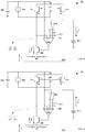
FIG. 1 , a block diagram of an exemplary circuit configuration with a current sense circuit according to an example of the present application is schematically illustrated. - The
exemplary circuit configuration 10 has aload transistor 110 and acurrent sense circuit 200 being coupled to asense transistor 120. Theload transistor 110 and thesense transistor 120 are of the same type and are illustrated as n-conductive MOSFETs by way of example inFIG. 1 . Theload transistor 110 and thesense transistor 120 may be in the form of any other desired transistor components, in particular as IGBTs. - In the example, a first load path terminal of the
load transistor 110 is formed by the drain terminal D thereof and a second load path terminal of thetransistor 110 is formed by the source terminal SP thereof. The gate terminal G forms the control terminal of theload transistor 110. Theload transistor 110 is connected in series with aload 300 and between the low-potential side Out of theload 300 and ground. - A
voltage power source 400 is further connected to the high-potential side In of theload 300 and applies a voltage at the series circuit between the supply potential Vdd of thesource 400 and the reference potential of ground. This configuration is usually called a low-side-drive configuration. Theload transistor 110, when enabled by acontrol voltage signal 500 at its gate terminal G, will pull the low potential side Out of theload 300 through the load path established between drain terminal D and the source terminal SP of theload terminal 110 to a low voltage, which substantially corresponds to the reference potential of ground. - The
sense transistor 120 likewise has a first sense path terminal, which is formed by the drain terminal D thereof, and a second sense path terminal, which is formed by a source terminal SM thereof. The control terminal of thesense transistor 120 is formed by the gate terminal G thereof and enables to switch the sense path between the drain terminal D and the source terminal SM of thesense transistor 120. - The drain terminal D of the
sense transistor 120 is connected to the drain terminal D of theload transistor 110. Further, the gate terminal G of thesense transistor 120 is connected to the gate terminal G of theload transistor 110. - In order to measure the current, the
sense transistor 120 is operated at substantially the same operating point as theload transistor 110. For this purpose, thesense transistor 120 is coupled to acurrent sense circuit 200 having a differential difference amplifier, DDA, 210, anauxiliary transistor 220 and acurrent measurement arrangement 230. - For the purpose of illustrating the mode of operation, the low-potential side Out of the
load 300 is connected to the drain terminal D of theload transistor 110, which is the first load path terminal thereof. - In the illustrated example, the
auxiliary transistor 220 is likewise in the form of n-conductive MOSFETs, the drain-source path of which is connected in series with the source-drain path of thesense transistor 120. The differential difference amplifier, DDA, 210 is connected between the drain terminal D and the source terminal SP of theload transistor 110 and further between the drain terminal D and the source terminal SM of thesense transistor 120. In particular, the drain terminal D and the source terminal SP of theload transistor 110 are connected to a first differential input terminal pair and the drain terminal D and the source terminal SM of thesense transistor 120 are connected to a second differential input terminal pair. At the first differential input terminal pair, the potential difference signal ΔVP between the drain terminal D and the source terminal SP of theload transistor 110 is applied and at the second differential input terminal pair, the potential difference signal ΔVS between the drain terminal D and the source terminal SM of thesense transistor 120 is applied. - In the illustrated example, in order to allow the
differential difference amplifier 210 to drive the control gate of theauxiliary transistor 220 so as to draw the sense current Isense from the source terminal SM of thesense transistor 120, the source terminal SP of theload transistor 110 and the source terminal SM of thesense transistor 120 are connected inverting inputs of the first and second differential input terminal pairs of the differential difference amplifier, DDA, 210. The (common) drain terminal(s) D of theload transistor 110 and thesense transistor 120 are connected to non-inverting inputs of the first and second differential input terminal pairs. The polarities of the potential difference signal ΔVP across theload transistor 110 and the potential difference signal ΔVS across thesense transistor 110 as applied to the differential input terminal pairs of the differential difference amplifier, DDA, 210 are different. - The differential difference amplifier, DDA, 210 drives a control gate of the
auxiliary transistor 220. The differential difference amplifier, DDA, 210 compares the potential difference signal ΔVP between the drain terminal D and the source terminal SP of theload transistor 110 and the potential difference signal ΔVS between the drain terminal D and the source terminal SM of thesense transistor 120 and sets theauxiliary transistor 220 by an output voltage signal of the differential difference amplifier, DDA, 210 at a control gate terminal of theauxiliary transistor 220 such that these potential differences match. The output voltage signal of the differential difference amplifier, DDA, 210 drives the control gate terminal of the firstauxiliary transistor 220 accordingly. - A load current Iload flows through the
load transistor 110, when theload 300 is connected through the load path switched conductive by thecontrol voltage signal 500 applied to the control gate G of theload transistor 110, while a sense current Isense flows through thesense transistor 120, when the sense path is switched conductive by thecontrol voltage signal 500 applied to the control gate G of thesense transistor 120. The sense current Isense flowing through the source-drain path of theauxiliary transistor 220 is proportional to the load current Iload flowing through theload 300 and through the drain-source load path of theload transistor 110, respectively:
- For the purpose of detecting the sense current Isense, the
current measuring arrangement 230, is connected in series with theauxiliary transistor 220. Thecurrent measuring arrangement 230 output a signal OutM, which is proportional to the load current Iload. - Referring now to
FIG. 2 , a block diagram of another exemplary circuit configuration with a current sense circuit according to an example of the present application is schematically illustrated. - The
exemplary circuit configuration 20 has aload transistor 110 and acurrent sense circuit 200 being coupled to asense transistor 120. Theload transistor 110 and thesense transistor 120 are of the same type and are illustrated as n-conductive MOSFETs by way of example inFIG. 2 . Theload transistor 110 and thesense transistor 120 may be in the form of any other desired transistor components, in particular as IGBTs. - In the example, a first load path terminal of the
load transistor 110 is formed by the drain terminal D thereof and a second load path terminal of thetransistor 110 is formed by the source terminal SP thereof. The gate terminal G forms the control terminal of theload transistor 110. Theload transistor 110 is connected in series with aload 300 and between the high potential side In and high-potential side Out. - A
voltage power source 400 is further connected to the high-potential side In and applies a voltage at the series circuit between the supply potential Vdd of thesource 400 and the reference potential of ground. Theload transistor 110, when enabled by acontrol voltage signal 500 at its gate terminal G, will pull the high-potential side Out of theload 300 through the load path established between drain terminal D and the source terminal SP of theload terminal 110 to a high voltage, which substantially corresponds to the supply potential Vdd. - This configuration is called a high-side-drive configuration. Comparing to conventional high-side-drive configuration, one skilled in the art could find that the power source and the load are exchanged by their positions, which, for this particular case illustration, may take place, for example, in automotive dual battery systems in start-stop or in H-bridge applications.
- The
sense transistor 120 likewise has a first sense path terminal, which is formed by the drain terminal D thereof, and a second sense path terminal, which is formed by a source terminal SM thereof. The control terminal of thesense transistor 120 is formed by the gate terminal G thereof and enables to switch the sense path between the drain terminal D and the source terminal SM of thesense transistor 120. - The drain terminal D of the
sense transistor 120 is connected to the drain terminal D of theload transistor 110. Further, the gate terminal G of thesense transistor 120 is connected to the gate terminal G of theload transistor 110. - In order to measure the current, the
sense transistor 120 is operated at substantially the same operating point as theload transistor 110. For this purpose, thesense transistor 120 is coupled to acurrent sense circuit 200 having a differential difference amplifier, DDA, 210, anauxiliary transistor 220 and acurrent measurement arrangement 230. - For the purpose of illustrating the mode of operation, the high-potential side Out of the
load 300 is connected to the drain terminal D of theload transistor 110, which is the first load path terminal thereof. - In the illustrated example, the
auxiliary transistor 220 is likewise in the form of p-conductive MOSFETs. The drain-source path of thesense transistor 120 is connected in series with the source-drain path of theauxiliary transistor 220. The differential difference amplifier, DDA, 210 is connected between the drain terminal D and the source terminal SP of theload transistor 110 and further between the drain terminal D and the source terminal SM of thesense transistor 120. In particular, the drain terminal D and the source terminal SP of theload transistor 110 are connected to a first differential input terminal pair and the drain terminal D and the source terminal SM of thesense transistor 120 are connected to a second differential input terminal pair. At the first differential input terminal pair, the potential difference signal ΔVP between the drain terminal D and the source terminal SP of theload transistor 110 is applied and at the second differential input terminal pair, the potential difference signal ΔVS between the drain terminal D and the source terminal SM of thesense transistor 120 is applied. - In the illustrated example, in order to allow the
differential difference amplifier 210 to drive the control gate of theauxiliary transistor 220 so as to draw the sense current Isense from the source terminal SM of thesense transistor 120, the source terminal SP of theload transistor 110 and the source terminal SM of thesense transistor 120 are connected non-inverting inputs of the first and second differential input terminal pairs of the differential difference amplifier, DDA, 210. The (common) drain terminal(s) D of theload transistor 110 and thesense transistor 120 are connected to inverting inputs of the first and second differential input terminal pairs. The polarities of the potential difference signal ΔVP across theload transistor 110 and the potential difference signal ΔVS across thesense transistor 110 as applied to the differential input terminal pairs of the differential difference amplifier, DDA, 210 are different. - The differential difference amplifier, DDA, 210 drives a control gate of the
auxiliary transistor 220. The differential difference amplifier, DDA, 210 compares the potential difference signal between the drain terminal D and the source terminal SP of theload transistor 110 and the potential difference signal ΔVS between the drain terminal D and the source terminal SM of thesense transistor 120 and sets theauxiliary transistor 220 by an output voltage signal of the differential difference amplifier, DDA, 210 at a control gate terminal of theauxiliary transistor 220 such that these potential differences match. The output voltage signal of the differential difference amplifier, DDA, 210 drives the control gate terminal of the firstauxiliary transistor 220 accordingly. - A load current Iload flows through the
load transistor 110, when theload 300 is connected through the load path switched conductive by thecontrol voltage signal 500 applied to the control gate G of theload transistor 110, while a measurement current Isense flows through thesense transistor 120, when the sense path is switched conductive by thecontrol voltage signal 500 applied to the control gate G of thesense transistor 120. The sense current Isense flowing through the source-drain path of theauxiliary transistor 220 is proportional to the load current Iload flowing through theload 300 and through the source-drain load path of theload transistor 110, respectively:
- For the purpose of detecting the sense current Isense, the
current measuring arrangement 230, is connected in series with theauxiliary transistor 220. Thecurrent measuring arrangement 230 output a signal OutM, which is proportional to the load current Iload. - Referring now to
FIG. 3a , a schematic block diagram of a differential difference amplifier, DDA, according to an example of the present application is illustrated. - Differential difference amplifiers are described in detail in the following references:
- 1. A. Soliman: "The Differential Difference Operational Floating Amplifier: A New Block for Analog Signal Processing in MOS Technology" IEEE Transactions on Circuits and Systems II, Vol. 45, No. 1, pp. 148-158, January 1998; and
- 2. E. Säckinger and W. Guggenbühl: "A Versatile Building Block: The CMOS Differential Difference Amplifier", EEEE Journal of Solid-Sate Circuits, Vol. SC-22, No. 2, pp. 287-294, April 1987.
- For the sake of understanding, a differential difference amplifier may be considered to comprise two input differential amplifiers each having a differential input terminal pair and a (open-loop) gain A0 = gm·AZ. Each differential input terminal pair is provided for receiving a voltage difference, herein the voltage difference Vpp - Vpn and the voltage difference Vnp - Vnn. The
input terminals input terminals - In the implementation of the differential difference amplifier described herein with reference to
FIG. 3a , a sum signal of the output signals of the input operation amplifiers is amplified by an output operational amplifier with a (open-loop) gain A0. The output signal vo of the output operational amplifier is
- In a closed loop operation, the differential difference amplifier forces two differential voltages to the same value, the basic equation that characterizes the operation of the differential difference amplifier is given by

input terminal 2 contributing to vpn, or at theinput terminal 4 contributing to vnn, and A0 → ∞. - Referring to
FIG. 3b , a schematic block diagram of an alternative differential difference amplifier, DDA, according to an example of the present application is illustrated. - Likewise, the alternative implementation of a differential difference amplifier may be considered to comprise two input differential amplifiers each having a differential input terminal pair and a (open-loop) gain A0 = gm·Az. Each differential input terminal pair is provided for receiving a voltage difference, herein the first voltage difference vpp - vpn and the second voltage difference vnp - vnn. The
input terminals input terminals - In the alternative implementation of the differential difference amplifier described herein with reference to
FIG. 3b , a difference signal of the output signals of the input operation amplifiers is amplified by an output operational amplifier with a (open-loop) gain A0. The output signal vo of the output operational amplifier is
- In a closed loop operation, the differential difference amplifier forces two differential voltages to the same value, the basic equation that characterizes the operation of the differential difference amplifier is given by

- Those skilled in the art will appreciate from the description of the present application that both implementations of a differential difference amplifier may be used.
- Referring now to
FIG. 4 , a schematic block diagram of an assembly comprising a load transistor and sense transistor according to an example of the present application is illustrated. - The assembly of load transistor and sense transistor as described throughout the present application may a
semiconductor arrangement 100 integrating two separate metal oxide semiconductor field effect transistor (MOSFET) components. A plurality of transistor cells may be integrated in thesemiconductor arrangement 100. At least one transistor cell forms thesense transistor 120 and a multiple of transistor cells form theload transistor 120. - The proportional factor k results from the ratio of the current conducting area of the load transistor and the current conducting area of the sense transistor, which is (at least approximately) equivalent to the ratio of the number of transistor cells in the load transistor and the sense transistor, respectively.
- Those skilled in the art understand that the present application is not limited to
semiconductor arrangement 100 as described above with reference toFIG. 4 . Theload transistor 110 and thesense transistor 120 may be also implemented in form of p- or n-channel metal-oxide-semiconductor field-effect transistor (MOSFET), junction gate field-effect transistor (JFET) or insulated-gate bipolar transistors (IGBTs) and the like. Due to technology constraints thesense transistor 120 and theload transistor 120 may have common drain electrode (not separable), which is in line with presented embodiment drawings of the invention. In some other particular cases sensetransistor 120 and theload transistor 120 may have common sense electrode, as technology constraint, which can be overcome by those, who skilled in the art, in the same manner as described in the present application by using a differential difference amplifier, DDA. - Referring now to
FIG. 5 , a schematic block diagram of a current measuring arrangement according to an example of the present application is illustrated. Thecurrent measuring arrangement 230 is configured to generate an output signal that is representative of the load current Iload. In the illustrated configuration example, thecurrent measuring arrangement 230 comprises a resistor RM, which is to be connected in series to thesense transistor 120 and theauxiliary transistor 220, respectively. Once the sense current Isense flows through the resistor RM, a voltage drop can be measured across the resistor RM:
- Those skilled in the art understand that the current measuring arrangement shown in
FIG. 5 is merely exemplary and not intended to limit the present application. Further current measuring arrangements known in the art may be used to measure the sense current Isense. - Referring now to
FIGs. 6 and 7 , a block diagram of a further exemplary circuit configuration with a current sense circuit according to an example of the present application is schematically illustrated. In theexample circuit configuration 30, the load current Iload may change its flow direction, the load current Iload may flow from acurrent source 450 to acurrent source 400 as illustrated inFIG. 6 and described below with reference thereto or from thesource 400 to thesource 450 as illustrated inFIG. 7 and described below with reference thereto. Thecircuit configuration 30 is implemented to allow for measuring of the load current Iload independent of the flow direction. - The
exemplary circuit configuration 30 has aload transistor 110, a firstcurrent sense circuit 200 and a secondcurrent sense circuit 250. Thecurrent sense circuits sense transistor 120. Theload transistor 110 and thesense transistor 120 are of the same type and are illustrated as n-conductive MOSFETs by way of example inFIGs. 6 and 7 . Theload transistor 110 and thesense transistor 120 may be in the form of any other desired transistor components, in particular as IGBTs. - In the example, a first load path terminal of the
load transistor 110 is formed by the drain terminal D thereof and a second load path terminal of thetransistor 110 is formed by the source terminal SP thereof. The gate terminal G forms the control terminal of theload transistor 110. Theload transistor 110 is connected in series between thesource 400 andsource 450. - The
source 400 and thesource 450 apply a voltage at the series circuit between the supply potential Vdd1 of thesource 400 and the supply potential Vdd2 of thesource 450. When theload transistor 110 is enabled by acontrol voltage signal 500 at its gate terminal G to establish the load path established between drain terminal D and the source terminal SP thereof, the load current Iload is driven by the one of thesources - The
sense transistor 120 likewise has a first sense path terminal, which is formed by the drain terminal D thereof, and a second sense path terminal, which is formed by a source terminal SM thereof. The control terminal of thesense transistor 120 is formed by the gate terminal G thereof and enables to switch the sense path between the drain terminal D and the source terminal SM of thesense transistor 120. - The drain terminal D of the
sense transistor 120 is connected to the drain terminal D of theload transistor 110. Further, the gate terminal G of thesense transistor 120 is connected to the gate terminal G of theload transistor 110. - For purpose of measuring the load current Iload independent of the flow direction, the
sense transistor 120 is coupled to acurrent sense circuit 200 and acurrent sense circuit 250. - The first
current sense circuit 200 has a differential difference amplifier, DDA, 210, a firstauxiliary transistor 220 and a firstcurrent measurement arrangement 230. In the illustrated example, the firstauxiliary transistor 220 is likewise in the form of p-conductive MOSFETs. The drain-source path of thesense transistor 120 is connected in series with the source-drain path of the firstauxiliary transistor 220. The differential difference amplifier, DDA, 210 is connected between the drain terminal D and the source terminal SP of theload transistor 110 and further between the drain terminal D and the source terminal SM of thesense transistor 120. The differential difference amplifier, DDA, 210 drives a control gate of the firstauxiliary transistor 220. In particular, the drain terminal D and the source terminal SP of theload transistor 110 are connected to a first differential input terminal pair and the drain terminal D and the source terminal SM of thesense transistor 120 are connected to a second differential input terminal pair. At the first differential input terminal pair, the potential difference signal ΔVP between the drain terminal D and the source terminal SP of theload transistor 110 is applied and at the second differential input terminal pair, the potential difference signal ΔVS between the drain terminal D and the source terminal SM of thesense transistor 120 is applied. - In the illustrated example, in order to allow the
differential difference amplifier 210 to drive the control gate of theauxiliary transistor 220 so as to draw the sense current Isense from the source terminal SM of thesense transistor 120, the source terminal SP of theload transistor 110 and the source terminal SM of thesense transistor 120 are connected non-inverting inputs of the first and second differential input terminal pairs of the differential difference amplifier, DDA, 210. The (common) drain terminal(s) D of theload transistor 110 and thesense transistor 120 are connected to inverting inputs of the first and second differential input terminal pairs. The polarities of the potential difference signal ΔVP across theload transistor 110 and the potential difference signal ΔVS across thesense transistor 110 as applied to the differential input terminal pairs of the differential difference amplifier, DDA, 210 are different. - The differential difference amplifier, DDA, 210 compares the potential difference signal between the drain terminal D and the source terminal SP of the
load transistor 110 and the potential difference signal ΔVS between the drain terminal D and the source terminal SM of thesense transistor 120 and sets the firstauxiliary transistor 220 by an output voltage signal of the differential difference amplifier, DDA, 210 at a control gate terminal of the firstauxiliary transistor 220 such that these potential differences match. - The second
current sense circuit 250 has adifferential amplifier 260, a secondauxiliary transistor 270 and a secondcurrent measurement arrangement 280. In the illustrated example, the secondauxiliary transistor 270 is likewise in the form of p-conductive MOSFETs. The drain-source path of thesense transistor 120 is connected in series with the source-drain path of the secondauxiliary transistor 270. Thedifferential amplifier 260 is connected between the source terminal SP of theload transistor 110 and the source terminal SM of thesense transistor 120. Thedifferential amplifier 260 drives a control gate of the secondauxiliary transistor 270. Thedifferential amplifier 260 compares the voltage potential at the source terminal SP of theload transistor 110 and the voltage potential at the source terminal SM of thesense transistor 120. The secondcurrent sense circuit 250 represents a conventional circuit and method of current sensing, known in the art. - In
FIG. 6 , the load current Iload flows from thesource 450 to thesource 400 through theload transistor 110, when enabled by acontrol voltage signal 500 at its gate terminal G, while a measurement current Isense flows through thesense transistor 120, when the sense path is switched conductive by thecontrol voltage signal 500 applied to the control gate G of thesense transistor 120. - Herein, the flow direction of the load current Iload is from the drain terminal D to the source terminal SP of the
load transistor 110 and the flow direction of the sense current Isense is from the drain terminal D to the source terminal SM of thesense transistor 120; hence, the same current flow direction with respect to drain and source terminals. - The
differential amplifier 260 drives the control gate of the secondauxiliary transistor 270 so as to draw the sense current Isense from the source terminal SM of thesense transistor 120. The feedback action of thedifferential amplifier 260 and the secondauxiliary transistor 270 causes the voltage potential at the source terminal SM of thesense transistor 120 to be held equal to the voltage potential at the source terminal SP of theload transistor 110. The sense current Isense flowing through the source-drain path of the secondauxiliary transistor 270 is hence proportional to the load current Iload flowing through the source-drain load path of the load transistor 110:
- For the purpose of detecting the sense current Isense, the second current measuring
arrangement 280, is connected in series with the secondauxiliary transistor 270. Thecurrent measuring arrangement 280 output a signal OutM, which is proportional to the load current Iload. - The differential difference amplifier, DDA, 210 is unable to drive the control gate of the first
auxiliary transistor 220 to cause a feedback action, in response to which the potential difference signal ΔVP between the drain terminal D and the source terminal SP of theload transistor 110 and the potential difference signal ΔVS between the drain terminal D and the source terminal SM of thesense transistor 120 are held equal by setting the firstauxiliary transistor 220 by the output voltage signal of the differential difference amplifier, DDA, 210 at a control gate terminal of the firstauxiliary transistor 220 such that these potential differences match. - In
FIG. 7 , the load current Iload flows from thesource 400 to thesource 450 through theload transistor 110, when enabled by acontrol voltage signal 500 at its gate terminal G, while a measurement current Isense flows through thesense transistor 120, when the sense path is switched conductive by thecontrol voltage signal 500 applied to the control gate G of thesense transistor 120. - Herein, the flow direction of the load current Iload is from the source terminal SP to the drain terminal D of the
load transistor 110 and the flow direction of the sense current Isense is from the drain terminal D to the source terminal SM of thesense transistor 120; hence, different current flow directions with respect to drain and source terminals. - The differential difference amplifier, DDA, 210 drives the control gate of the first
auxiliary transistor 220 so as to draw the sense current Isense from the source terminal SM of thesense transistor 120. - The differential difference amplifier, DDA, 210 compares the potential difference signal between the drain terminal D and the source terminal SP of the
load transistor 110 and the potential difference signal ΔVS between the drain terminal D and the source terminal SM of thesense transistor 120. The feedback action of the differential difference amplifier, DDA, 210 and the firstauxiliary transistor 220 causes the potential difference signal ΔVP across theload transistor 110 and the potential difference signal ΔVS across the sense transistor to be held equal. The feedback action is controlled by the output voltage signal of the differential difference amplifier, DDA, 210 driving the control gate terminal of the firstauxiliary transistor 220. The sense current Isense flowing through the source-drain path of the firstauxiliary transistor 220 is hence proportional to the load current Iload flowing through the source-drain load path of the load transistor 110:
- For the purpose of detecting the sense current Isense, the first
current measuring arrangement 230, is connected in series with the firstauxiliary transistor 220. Thecurrent measuring arrangement 230 output a signal OutM, which is proportional to the load current Iload. - The
differential amplifier 260 is unable to drive the control gate of the secondauxiliary transistor 270 to cause a feedback action, in response to which the voltage potential at the source terminal SP of theload transistor 110 and the voltage potential at the source terminal SM of thesense transistor 120 are held equal by setting the secondauxiliary transistor 270 by the output voltage signal of thedifferential amplifier 260 at a control gate terminal of the firstauxiliary transistor 220 such that these potential differences match. - Referring now to
FIGs. 6 and 7 , a block diagram of yet another exemplary circuit configuration with a current sense circuit according to an example of the present application is schematically illustrated. - In the
example circuit configuration 40, the load current Iload may change its flow direction, the load current Iload may flow from acurrent source 450 to acurrent source 400 as illustrated inFIG. 8 and described below with reference thereto or from thesource 400 to thesource 450 as illustrated inFIG. 9 and described below with reference thereto. Thecircuit configuration 40 is implemented to allow for measuring of the load current load independent of the flow direction. - The
exemplary circuit configuration 40 has aload transistor 110 and acurrent sense circuit 200. Thecurrent sense circuit 200 is coupled to asense transistor 120. Theload transistor 110 and thesense transistor 120 are of the same type and are illustrated as n-conductive MOSFETs by way of example inFIGs. 6 and 7 . Theload transistor 110 and thesense transistor 120 may be in the form of any other desired transistor components, in particular as IGBTs. - In the example, a first load path terminal of the
load transistor 110 is formed by the drain terminal D thereof and a second load path terminal of thetransistor 110 is formed by the source terminal SP thereof. The gate terminal G forms the control terminal of theload transistor 110. Theload transistor 110 is connected in series between thesource 400 andsource 450. - The
source 400 and thesource 450 apply a voltage at the series circuit between the supply potential Vdd1 of thesource 400 and the supply potential Vdd2 of thesource 450. When theload transistor 110 is enabled by acontrol voltage signal 500 at its gate terminal G to establish the load path established between drain terminal D and the source terminal SP thereof, the load current Iload is driven by the one of thesources - The
sense transistor 120 likewise has a first sense path terminal, which is formed by the drain terminal D thereof, and a second sense path terminal, which is formed by a source terminal SM thereof. The control terminal of thesense transistor 120 is formed by the gate terminal G thereof and enables to switch the sense path between the drain terminal D and the source terminal SM of thesense transistor 120. - The drain terminal D of the
sense transistor 120 is connected to the drain terminal D of theload transistor 110. Further, the gate terminal G of thesense transistor 120 is connected to the gate terminal G of theload transistor 110. - The
current sense circuit 200 has a differential difference amplifier, DDA, 210, anauxiliary transistor 220 and acurrent measurement arrangement 230. In the illustrated example, theauxiliary transistor 220 is likewise in the form of p-conductive MOSFETs. The drain-source path of thesense transistor 120 is connected in series with the source-drain path of theauxiliary transistor 220. The differential difference amplifier, DDA, 210 is connected between the drain terminal D and the source terminal SP of theload transistor 110 and further between the drain terminal D and the source terminal SM of thesense transistor 120. In particular, the drain terminal D and the source terminal SP of theload transistor 110 are connected to a first differential input terminal pair and the drain terminal D and the source terminal SM of thesense transistor 120 are connected to a second differential input terminal pair. At the first differential input terminal pair, the potential difference signal ΔVP between the drain terminal D and the source terminal SP of theload transistor 110 is applied and at the second differential input terminal pair, the potential difference signal ΔVS between the drain terminal D and the source terminal SM of thesense transistor 120 is applied. - The differential difference amplifier, DDA, 210 drives a control gate of the first
auxiliary transistor 220. The differential difference amplifier, DDA, 210 compares the potential difference signal ΔVP at the terminals of theload transistor 110 and the potential difference signal ΔVS at the terminals of thesense transistor 120 and sets the firstauxiliary transistor 220 by an output voltage signal of the differential difference amplifier, DDA, 210 at a control gate terminal of the firstauxiliary transistor 220 such that these potential differences match. - For purpose of measuring the load current Iload independent of the flow direction, single-pole, double-throw (SPDT) switches 205 and 206 are arranged to selectively connect the non-inverting terminal of the first differential input terminal pair of the differential difference amplifier, DDA, 210 to the drain terminal D or the source terminal SP of the
load transistor 110 and to selectively connect the inverting terminal of the first differential input terminal pair of the differential difference amplifier, DDA, 210 to the source terminal SP or the drain terminal D of theload transistor 110. The two single-pole, double-throw (SPDT) switches are arranged to selectively switch the polarity of the potential difference signal ΔVP applied to a differential input terminal pair of the differential difference amplifier, DDA, 210. - In
FIG. 8 , the load current Iload flows from thesource 450 to thesource 400 through theload transistor 110, when enabled by acontrol voltage signal 500 at its gate terminal G, while a measurement current Isense flows through thesense transistor 120, when the sense path is switched conductive by thecontrol voltage signal 500 applied to the control gate G of thesense transistor 120. Herein, the flow direction of the load current Iload is from the drain terminal D to the source terminal SP of theload transistor 110 and the flow direction of the sense current Isense is from the drain terminal D to the source terminal SM of thesense transistor 120; hence, the same current flow direction with respect to drain and source terminals. - In order to allow the
differential difference amplifier 210 to drive the control gate of theauxiliary transistor 220 so as to draw the sense current Isense from the source terminal SM of thesense transistor 120, the source terminal SP of theload transistor 110 and the source terminal SM of thesense transistor 120 are connected by the single-pole, double-throw (SPDT) switches to a non-inverting input of the first differential input terminal pair of the differential difference amplifier, DDA, 210 and an inverting terminal of the second differential input terminal pair thereof. Likewise the (common) drain terminal(s) D of theload transistor 110 and thesense transistor 120 is are connected by the single-pole, double-throw (SPDT) switches to an inverting input of the first differential input terminal pair of the differential difference amplifier, DDA, 210 and a non-inverting input of the second differential input terminal pair thereof. - The single-pole, double-throw (SPDT) switches are operated to switch the polarity of the potential difference signal ΔVP across the
load transistor 110 as applied to the first differential input terminal pair of the differential difference amplifier, DDA, 210 such that the polarities of the potential difference signal ΔVP across theload transistor 110 and the potential difference signal ΔVS across thesense transistor 110 as applied to the differential input terminal pairs are different. - In
FIG. 9 , the load current Iload flows from thesource 400 to thesource 450 through theload transistor 110, when enabled by acontrol voltage signal 500 at its gate terminal G, while a measurement current Isense flows through thesense transistor 120, when the sense path is switched conductive by thecontrol voltage signal 500 applied to the control gate G of thesense transistor 120. Herein, the flow direction of the load current Iload is from the source terminal SP to the drain terminal D of theload transistor 110 and the flow direction of the sense current Isense is from the drain terminal D to the source terminal SM of thesense transistor 120; hence, the different current flow directions with respect to drain and source terminals. - In order to allow the
differential difference amplifier 210 to drive the control gate of theauxiliary transistor 220 so as to draw the sense current Isense from the source terminal SM of thesense transistor 120, the source terminal SP of theload transistor 110 and the source terminal SM of thesense transistor 120 are connected by the single-pole, double-throw (SPDT) switches to non-inverting inputs of the first and second differential input terminal pairs of the differential difference amplifier, DDA, 210. Likewise the (common) drain terminal(s) D of theload transistor 110 and thesense transistor 120 are connected by the single-pole, double-throw (SPDT) switches to inverting inputs of the first and second differential input terminal pairs. - The single-pole, double-throw (SPDT) switches are operated to switch the polarity of the potential difference signal ΔVP across the
load transistor 110 as applied to the first differential input terminal pair of the differential difference amplifier, DDA, 210 such that the polarities of the potential difference signal ΔVP across theload transistor 110 and the potential difference signal ΔVS across thesense transistor 110 as applied to the differential input terminal pairs are different. - By means of the current flow direction based polarity switching, the feedback action of the differential difference amplifier, DDA, 210 and the
auxiliary transistor 220 is enabled to cause the potential difference signal ΔVP across theload transistor 110 and the potential difference signal ΔVS across thesense transistor 120 to be held equal independent of the current flow direction. The feedback action is controlled by the output voltage signal of the differential difference amplifier, DDA, 210 driving the control gate terminal of theauxiliary transistor 220. The sense current Isense flowing through the source-drain path of theauxiliary transistor 220 is hence proportional to the load current Iload flowing through the drain-source/source-drain load path of the load transistor 110:
- For the purpose of detecting the sense current Isense, the
current measuring arrangement 230, is connected in series with theauxiliary transistor 220. Thecurrent measuring arrangement 230 output a signal OutM, which is proportional to the value of the load current Iload. The signal OutM is independent on the flow direction of the load current Iload. - It should be noted that the two single-pole, double-throw (SPDT) switches should be understood to represent merely one possible implementation to selectively switch the polarity of the potential difference signal ΔVP. Alternative switching elements to selectively switch the polarity of the potential difference signal ΔVP may be used. For example, switch the polarity can be made inside the differential difference amplifier, DDA, 210, e.g. by alternating between the differential difference amplifier, DDA, configurations shown on
FIG. 3a and FIG. 3b . Further, switching elements such as the two single-pole, double-throw (SPDT) switches may be arranged to selectively switch the polarity of the potential difference signal ΔVS applied to a differential input terminal pair of the differential difference amplifier, DDA, 210. In particular, the two single-pole, double-throw (SPDT) switches may be implemented as one double-pole, double-throw (DPDT) switch. - Alternatively, one or more switching elements to selectively switch the polarity of the potential difference signal ΔVP may be used. Moreover, a switch operating signal may be generated based on the polarity of the potential difference signal ΔVP across the drain terminal D and the source terminal SP of the
load transistor 110, e.g. by using a differential amplifier comparing the voltage potential at the drain terminal D and the voltage potential at the source terminal SP of theload transistor 110. A hysteresis control may be applied to prevent from fast switching when the voltage potentials of thesources - In extend, inputs of the differential difference amplifier, DDA, can be switched with respect to description of previous invention (
US 20130057241 , Power switching apparatus and method for improving current sense accuracy) to decrease effect and inaccuracy of current sensing caused by the offset of the differential difference amplifier, DDA. - According to an embodiment, a current sense circuit is provided, which comprises a differential difference amplifier having a first differential input terminal pair coupled across a drain electrode and a source electrode of a load transistor; and a second differential input terminal pair coupled across a drain electrode and a source electrode of a sense transistor. The current sense circuit is operable to force the same voltage difference value across the drain electrode and the source electrode of the load transistor as across the drain electrode and the source electrode of the sense transistor to cause a sense current through the sense transistor. The sense current is representative of a load current through the load transistor.
- According to an example, the current sense circuit further comprises an auxiliary transistor coupled in series with the sense transistor. A control gate electrode of the auxiliary transistor is coupled to the output terminal of the differential difference amplifier, the differential difference amplifier and the auxiliary transistor forming a feedback circuit. According to an example, a source electrode of the auxiliary transistor is coupled to sense transistor. According to an example, the differential difference amplifier is responsively coupled to the source electrode of the sense transistor. According to an example, the current sense circuit is operable to cause the sense current through sense transistor having a current flow direction opposite to the load current through the load transistor with respect to the source-drain path. According to an example, the sense current is proportional to the load current. According to an example, the current sense circuit further comprises at least one switching element coupled between the source electrode and drain electrode of the load transistor and the first differential input terminal pair and operable to switch the polarity of the first voltage difference signal of the potential difference between the drain electrode and the source electrode of the load transistor dependent on the current flow direction of the load current. According to an example, the at least one switching element comprises one of a double-pole, double-throw (DPDT) switch and two single-pole, double-throw switches. According to an example, the current sense circuit further comprises a current measuring arrangement coupled in series with the sense transistor and arranged to output an output signal being representative of the load current. According to an example, the output signal is proportional to the load current.
- According to an embodiment, a circuit arrangement is provided, which comprises a load transistor coupled in series with and configured to control a load current to a load; a sense transistor that provides a sense current; and a current sense circuit coupled in series with the sense transistor, comprising: a differential difference amplifier. The differential difference amplifier has a first differential input terminal pair coupled across a drain electrode and a source electrode of a load transistor; and a second differential input terminal pair coupled across a drain electrode and a source electrode of a sense transistor. The current sense circuit is operable to force the same voltage difference value across the drain electrode and the source electrode of the load transistor as across the drain electrode and the source electrode of the sense transistor to cause a sense current through the sense transistor. The sense current is representative of a load current through a load transistor.
- According to an example, a first voltage difference signal of a potential difference between the drain electrode and the source electrode of the load transistor is provided to the first differential input terminal pair. A second voltage difference signal of a potential difference between the drain electrode and the source electrode of the sense transistor is provided to the second differential input terminal pair. According to an example, the load transistor and the sense transistor have a common drain electrode. According to an example, the load transistor and the sense transistor have a common gate electrode. According to an example, the load transistor and the sense transistor are arranged in an integrated semiconductor device. According to an example, the current sense circuit corresponds to the aforementioned current sense circuit. According to an example, the load is coupled to the one or the source electrode and the drain electrode of the load transistor. According to an example, the load transistor and/or the sense transistor is at least one of a field effect transistor, a metal-oxide-semiconductor field effect transistor and an insulated-gate bipolar transistor.
- According to an example, the circuit arrangement further comprises another current sense circuit configured to cause the sense current through the sense transistor, the sense current being representative of the load current. The other current sense circuit comprises a differential amplifier has a first input terminal coupled to one of the source and the drain electrode of the load transistor to receive a voltage potential signal thereof; and a second input terminal coupled to one of the source and the drain electrode of the sense transistor to receive a voltage potential signal thereof. The other current sense circuit is operable to force the same voltage across the load transistor as across the sense transistor. The other current sense circuit is operable to cause the sense current through sense transistor having the current flow direction as the load current through the load transistor with respect to the source-drain path. According to an example, the another current sense circuit further comprises an auxiliary transistor coupled in series with the sense transistor. A control gate electrode of the auxiliary transistor is coupled to the output terminal of the differential amplifier, the differential amplifier and the auxiliary transistor forming a feedback circuit.
- Those of skill in the art would understand that information and signals may be represented using any of a variety of different technologies and techniques. For example, data, instructions, commands, information, signals, bits, symbols, and chips that may be referenced throughout the above description may be represented by voltages, currents, electromagnetic waves, magnetic fields or particles, optical fields or particles, or any combination thereof.
- Those of skill would further appreciate that the various illustrative logical blocks, modules, circuits, and algorithm steps described in connection with the disclosure herein may be implemented as electronic hardware, computer software, or combinations of both. To illustrate clearly this interchangeability of hardware and software, various illustrative components, blocks, modules, circuits, and steps have been described above generally in terms of their functionality. Whether such functionality is implemented as hardware or software depends upon the particular application and design constraints imposed on the overall system. Skilled artisans may implement the described functionality in varying ways for each particular application, but such implementation decisions should not be interpreted as causing a departure from the scope of the present disclosure.
- In the claims, any reference signs placed between parentheses shall not be construed as limiting the claim. The word "comprising" does not exclude the presence of other elements or operations then those listed in a claim. Furthermore, the terms "a" or "an", as used herein, are defined as one or as more than one. Also, the use of introductory phrases such as "at least one" and "one or more" in the claims should not be construed to imply that the introduction of another claim element by the indefinite articles "a" or "an" limits any particular claim containing such introduced claim element to inventions containing only one such element, even when the same claim includes the introductory phrases "one or more" or "at least one" and indefinite articles such as "a" or "an". The same holds true for the use of definite articles. Unless stated otherwise, terms such as "first" and "second" are used to distinguish arbitrarily between the elements such terms describe. Thus, these terms are not necessarily intended to indicate temporal or other prioritization of such elements. The mere fact that certain measures are recited in mutually different claims does not indicate that a combination of these measures cannot be used to advantage.
- The previous description of the disclosure is provided to enable any person skilled in the art to make or use the disclosure. Various modifications to the disclosure will be readily apparent to those skilled in the art, and the generic principles defined herein may be applied to other variations without departing from the spirit or scope of the disclosure. Thus, the disclosure is not intended to be limited to the examples and designs described herein but is to be accorded the widest scope consistent with the principles and novel features disclosed herein.
Claims (15)
- A current sense circuit, comprising:a differential difference amplifier (210) havinga first differential input terminal pair coupled across a drain electrode and a source electrode of a load transistor (110); anda second differential input terminal pair coupled across a drain electrode and a source electrode of a sense transistor,wherein the current sense circuit (200) is operable to force the same voltage difference value across the drain electrode and the source electrode of the load transistor as across the drain electrode and the source electrode of the sense transistor to cause a sense current through the sense transistor (120),wherein the sense current is representative of a load current through the load transistor.
- The current sense circuit according to claim 1, further comprising:an auxiliary transistor (220) coupled in series with the sense transistor,wherein a control gate electrode of the auxiliary transistor is coupled to the output terminal of the differential difference amplifier, the differential difference amplifier and the auxiliary transistor forming a feedback circuit.
- The current sense circuit according to claim 2,
wherein a source electrode of the auxiliary transistor is coupled to sense transistor. - The current sense circuit according to any one of the claims 1 to 3,
wherein the differential difference amplifier is responsively coupled to the source electrode of the sense transistor. - The current sense circuit according to claim 1,
wherein the current sense circuit is operable to cause the sense current through sense transistor having a current flow direction opposite to the load current through the load transistor with respect to the source-drain path. - The current sense circuit according to claim 1,
wherein the sense current is proportional to the load current. - The current sense circuit according to claim 1, further comprising:at least one switching element (205, 206) coupled between the source electrode and drain electrode of the load transistor and the first differential input terminal pair and operable to switch the polarity of the first voltage difference signal of the potential difference between the drain electrode and the source electrode of the load transistor dependent on the current flow direction of the load current.
- The circuit arrangement according to claim 7,
wherein the at least one switching element comprises one of a double-pole, double-throw, DPDT, switch and two single-pole, double-throw switches, SPDT. - A circuit arrangement, comprising
a load transistor (110) coupled in series with and configured to control a load current to a load (300);
a sense transistor (120) that provides a sense current; and
a current sense circuit (200) coupled in series with the sense transistor, comprising:a differential difference amplifier (210) havinga first differential input terminal pair coupled across a drain electrode and a source electrode of a load transistor; anda second differential input terminal pair coupled across a drain electrode and a source electrode of a sense transistor,wherein the current sense circuit is operable to force the same voltage difference value across the drain electrode and the source electrode of the load transistor as across the drain electrode and the source electrode of the sense transistor to cause a sense current through the sense transistor,
wherein the sense current is representative of a load current through the load transistor. - The circuit arrangement according to claim 9,
wherein a first voltage difference signal of a potential difference between the drain electrode and the source electrode of the load transistor is provided to the first differential input terminal pair,
wherein a second voltage difference signal of a potential difference between the drain electrode and the source electrode of the sense transistor is provided to the second differential input terminal pair. - The circuit arrangement according to claim 9 or claim 10,
wherein the load transistor and the sense transistor have a common drain electrode and/or a common gate electrode. - The circuit arrangement according to any one of the claims 9 to 12,
wherein the current sense circuit is a current sense circuit according to any one of claims 1 to 8. - The circuit arrangement according to any one of the claims 9 to 13,
wherein the load is coupled to the one of the source electrode and the drain electrode of the load transistor. - The circuit arrangement according to claim 9, further comprising:another current sense circuit (250) configured to cause the sense current through the sense transistor, the sense current being representative of the load current, the other current sense circuit comprising:a differential amplifier (260) havinga first input terminal coupled to one of the source and the drain electrode of the load transistor to receive a voltage potential signal thereof; anda second input terminal coupled to one of the source and the drain electrode of the sense transistor to receive a voltage potential signal thereof,wherein the other current sense circuit is operable to force the same voltage across the load transistor as across the sense transistor,wherein the other current sense circuit is operable to cause the sense current through sense transistor having the current flow direction as the load current through the load transistor with respect to the source-drain path.
- The circuit arrangement according to claim 16, wherein the another current sense circuit further comprises:an auxiliary transistor (270) coupled in series with the sense transistor,wherein a control gate electrode of the auxiliary transistor is coupled to the output terminal of the differential amplifier, the differential amplifier and the auxiliary transistor forming a feedback circuit.
Applications Claiming Priority (1)
| Application Number | Priority Date | Filing Date | Title |
|---|---|---|---|
| US14/983,835 US10156592B2 (en) | 2015-12-30 | 2015-12-30 | Current sensing circuit and method |
Publications (2)
| Publication Number | Publication Date |
|---|---|
| EP3187885A1 true EP3187885A1 (en) | 2017-07-05 |
| EP3187885B1 EP3187885B1 (en) | 2019-10-16 |
Family
ID=57754958
Family Applications (1)
| Application Number | Title | Priority Date | Filing Date |
|---|---|---|---|
| EP16204323.6A Active EP3187885B1 (en) | 2015-12-30 | 2016-12-15 | A current sensing circuit and method |
Country Status (2)
| Country | Link |
|---|---|
| US (1) | US10156592B2 (en) |
| EP (1) | EP3187885B1 (en) |
Families Citing this family (1)
| Publication number | Priority date | Publication date | Assignee | Title |
|---|---|---|---|---|
| US11835572B2 (en) * | 2021-04-06 | 2023-12-05 | International Business Machines Corporation | Usage metering by bias temperature instability |
Citations (3)
| Publication number | Priority date | Publication date | Assignee | Title |
|---|---|---|---|---|
| US20060028192A1 (en) * | 2004-08-02 | 2006-02-09 | Matsushita Electric Industrial Co., Ltd. | Current detection circuit and switching power supply using the same |
| US20060255783A1 (en) * | 2005-05-10 | 2006-11-16 | Power-One Limited | Bi-directional MOS current sense circuit |
| US20130057241A1 (en) | 2010-05-21 | 2013-03-07 | Freescale Semiconductor, Inc. | Power switching apparatus and method for improving current sense accuracy |
Family Cites Families (11)
| Publication number | Priority date | Publication date | Assignee | Title |
|---|---|---|---|---|
| IT1213415B (en) | 1986-12-17 | 1989-12-20 | Sgs Microelettronica Spa | CIRCUIT FOR LINEAR MEASUREMENT OF THE CIRCULATING CURRENT ON A LOAD. |
| US5498984A (en) | 1994-09-30 | 1996-03-12 | Maxim Integrated Products | High side, current sense amplifier using a symmetric amplifier |
| DE10240914B4 (en) | 2002-09-04 | 2007-01-25 | Infineon Technologies Ag | Circuit arrangement with a load transistor and a current measuring arrangement and method for determining the load current of a load transistor and use of a semiconductor device |
| DE10258766B4 (en) | 2002-12-16 | 2005-08-25 | Infineon Technologies Ag | Circuit arrangement for controlling and detecting the load current through a load |
| US7034542B2 (en) | 2004-02-24 | 2006-04-25 | Texas Instruments Incorporated | Current sensing circuit and method |
| EP1681761A1 (en) | 2005-01-14 | 2006-07-19 | Dialog Semiconductor GmbH | Current sensing structure for integrated power switches |
| US8018213B2 (en) | 2008-09-29 | 2011-09-13 | Infineon Technologies Ag | Measuring the current through a load transistor |
| US8237449B2 (en) | 2010-05-27 | 2012-08-07 | Standard Microsystems Corporation | Bi-directional high side current sense measurement |
| EP2515126A1 (en) | 2011-04-19 | 2012-10-24 | Dialog Semiconductor GmbH | Bidirectional current sense |
| US9664713B2 (en) * | 2014-10-30 | 2017-05-30 | Infineon Technologies Austria Ag | High speed tracking dual direction current sense system |
| DE102015204518B4 (en) * | 2015-03-12 | 2017-04-13 | Dialog Semiconductor (Uk) Limited | Offset compensation for a VDS compensator in a current detection circuit |
-
2015
- 2015-12-30 US US14/983,835 patent/US10156592B2/en active Active
-
2016
- 2016-12-15 EP EP16204323.6A patent/EP3187885B1/en active Active
Patent Citations (3)
| Publication number | Priority date | Publication date | Assignee | Title |
|---|---|---|---|---|
| US20060028192A1 (en) * | 2004-08-02 | 2006-02-09 | Matsushita Electric Industrial Co., Ltd. | Current detection circuit and switching power supply using the same |
| US20060255783A1 (en) * | 2005-05-10 | 2006-11-16 | Power-One Limited | Bi-directional MOS current sense circuit |
| US20130057241A1 (en) | 2010-05-21 | 2013-03-07 | Freescale Semiconductor, Inc. | Power switching apparatus and method for improving current sense accuracy |
Non-Patent Citations (2)
| Title |
|---|
| A. SOLIMAN: "The Differential Difference Operational Floating Amplifier: A New Block for Analog Signal Processing in MOS Technology", IEEE TRANSACTIONS ON CIRCUITS AND SYSTEMS II, vol. 45, no. 1, January 1998 (1998-01-01), pages 148 - 158, XP011012754 |
| E. SACKINGER; W. GUGGENBUH!: "A Versatile Building Block: The CMOS Differential Difference Amplifier", EEEE JOURNAL OF SOLID-SATE CIRCUITS, vol. SC-22, no. 2, April 1987 (1987-04-01), pages 287 - 294, XP000195792, DOI: doi:10.1109/JSSC.1987.1052715 |
Also Published As
| Publication number | Publication date |
|---|---|
| US10156592B2 (en) | 2018-12-18 |
| EP3187885B1 (en) | 2019-10-16 |
| US20170192040A1 (en) | 2017-07-06 |
Similar Documents
| Publication | Publication Date | Title |
|---|---|---|
| EP0294880B1 (en) | Differential amplifier and current sensing circuit including such an amplifier | |
| US9829387B2 (en) | System and method for temperature sensing | |
| US10018658B2 (en) | Class D audio amplifier and method for reading a current supplied by the amplifier | |
| US8018213B2 (en) | Measuring the current through a load transistor | |
| US7202711B2 (en) | Technique for determining a load current | |
| US6977513B2 (en) | Current detection circuit of bidirectional switch | |
| US7759982B2 (en) | Current detection circuit | |
| US7005881B2 (en) | Current sensing for power MOSFET operable in linear and saturated regions | |
| US20140184184A1 (en) | Voltage detecting circuit and voltage regulator apparatus provided with same | |
| CN109888855B (en) | Charge-discharge control device and battery device | |
| CN107810421B (en) | Voltage monitor | |
| JPH01227520A (en) | Power semiconductor device | |
| EP1088395A1 (en) | A power switching circuit | |
| EP1636600B1 (en) | Undercurrent sense arrangement and method | |
| US7268520B2 (en) | Sense amplifier for use with wake-up charging current | |
| EP2634806B1 (en) | Input protection circuit | |
| US9720030B2 (en) | Systems and methods for testing a clamp function for insulated gate bipolar transistors | |
| EP3187885B1 (en) | A current sensing circuit and method | |
| JP4894865B2 (en) | Bidirectional switch current detection circuit | |
| US7173476B2 (en) | Semiconductor integrated circuit device | |
| US7057445B2 (en) | Bias voltage generating circuit and differential amplifier | |
| EP3282581B1 (en) | Buffer stage and control circuit | |
| WO2022093449A1 (en) | Leakage compensation technique for current sensor | |
| US9281746B1 (en) | System and method for a diagnostic circuit | |
| CN112114257A (en) | Voltage-current conversion circuit and charge-discharge control device |
Legal Events
| Date | Code | Title | Description |
|---|---|---|---|
| PUAI | Public reference made under article 153(3) epc to a published international application that has entered the european phase |
Free format text: ORIGINAL CODE: 0009012 |
|
| STAA | Information on the status of an ep patent application or granted ep patent |
Free format text: STATUS: THE APPLICATION HAS BEEN PUBLISHED |
|
| AK | Designated contracting states |
Kind code of ref document: A1 Designated state(s): AL AT BE BG CH CY CZ DE DK EE ES FI FR GB GR HR HU IE IS IT LI LT LU LV MC MK MT NL NO PL PT RO RS SE SI SK SM TR |
|
| AX | Request for extension of the european patent |
Extension state: BA ME |
|
| STAA | Information on the status of an ep patent application or granted ep patent |
Free format text: STATUS: REQUEST FOR EXAMINATION WAS MADE |
|
| 17P | Request for examination filed |
Effective date: 20180105 |
|
| RBV | Designated contracting states (corrected) |
Designated state(s): AL AT BE BG CH CY CZ DE DK EE ES FI FR GB GR HR HU IE IS IT LI LT LU LV MC MK MT NL NO PL PT RO RS SE SI SK SM TR |
|
| STAA | Information on the status of an ep patent application or granted ep patent |
Free format text: STATUS: EXAMINATION IS IN PROGRESS |
|
| 17Q | First examination report despatched |
Effective date: 20181203 |
|
| RIC1 | Information provided on ipc code assigned before grant |
Ipc: G01R 17/16 20060101ALI20190416BHEP Ipc: G01R 19/00 20060101AFI20190416BHEP Ipc: H02M 3/156 20060101ALI20190416BHEP Ipc: H03K 17/12 20060101ALI20190416BHEP |
|
| GRAP | Despatch of communication of intention to grant a patent |
Free format text: ORIGINAL CODE: EPIDOSNIGR1 |
|
| STAA | Information on the status of an ep patent application or granted ep patent |
Free format text: STATUS: GRANT OF PATENT IS INTENDED |
|
| INTG | Intention to grant announced |
Effective date: 20190529 |
|
| GRAJ | Information related to disapproval of communication of intention to grant by the applicant or resumption of examination proceedings by the epo deleted |
Free format text: ORIGINAL CODE: EPIDOSDIGR1 |
|
| STAA | Information on the status of an ep patent application or granted ep patent |
Free format text: STATUS: EXAMINATION IS IN PROGRESS |
|
| GRAP | Despatch of communication of intention to grant a patent |
Free format text: ORIGINAL CODE: EPIDOSNIGR1 |
|
| STAA | Information on the status of an ep patent application or granted ep patent |
Free format text: STATUS: GRANT OF PATENT IS INTENDED |
|
| GRAS | Grant fee paid |
Free format text: ORIGINAL CODE: EPIDOSNIGR3 |
|
| INTC | Intention to grant announced (deleted) | ||
| GRAA | (expected) grant |
Free format text: ORIGINAL CODE: 0009210 |
|
| STAA | Information on the status of an ep patent application or granted ep patent |
Free format text: STATUS: THE PATENT HAS BEEN GRANTED |
|
| INTG | Intention to grant announced |
Effective date: 20190826 |
|
| AK | Designated contracting states |
Kind code of ref document: B1 Designated state(s): AL AT BE BG CH CY CZ DE DK EE ES FI FR GB GR HR HU IE IS IT LI LT LU LV MC MK MT NL NO PL PT RO RS SE SI SK SM TR |
|
| REG | Reference to a national code |
Ref country code: GB Ref legal event code: FG4D |
|
| REG | Reference to a national code |
Ref country code: CH Ref legal event code: EP |
|
| REG | Reference to a national code |
Ref country code: DE Ref legal event code: R096 Ref document number: 602016022498 Country of ref document: DE |
|
| REG | Reference to a national code |
Ref country code: IE Ref legal event code: FG4D |
|
| REG | Reference to a national code |
Ref country code: AT Ref legal event code: REF Ref document number: 1191791 Country of ref document: AT Kind code of ref document: T Effective date: 20191115 |
|
| REG | Reference to a national code |
Ref country code: NL Ref legal event code: MP Effective date: 20191016 |
|
| REG | Reference to a national code |
Ref country code: LT Ref legal event code: MG4D |
|
| REG | Reference to a national code |
Ref country code: AT Ref legal event code: MK05 Ref document number: 1191791 Country of ref document: AT Kind code of ref document: T Effective date: 20191016 |
|
| PG25 | Lapsed in a contracting state [announced via postgrant information from national office to epo] |
Ref country code: FI Free format text: LAPSE BECAUSE OF FAILURE TO SUBMIT A TRANSLATION OF THE DESCRIPTION OR TO PAY THE FEE WITHIN THE PRESCRIBED TIME-LIMIT Effective date: 20191016 Ref country code: PT Free format text: LAPSE BECAUSE OF FAILURE TO SUBMIT A TRANSLATION OF THE DESCRIPTION OR TO PAY THE FEE WITHIN THE PRESCRIBED TIME-LIMIT Effective date: 20200217 Ref country code: BG Free format text: LAPSE BECAUSE OF FAILURE TO SUBMIT A TRANSLATION OF THE DESCRIPTION OR TO PAY THE FEE WITHIN THE PRESCRIBED TIME-LIMIT Effective date: 20200116 Ref country code: PL Free format text: LAPSE BECAUSE OF FAILURE TO SUBMIT A TRANSLATION OF THE DESCRIPTION OR TO PAY THE FEE WITHIN THE PRESCRIBED TIME-LIMIT Effective date: 20191016 Ref country code: GR Free format text: LAPSE BECAUSE OF FAILURE TO SUBMIT A TRANSLATION OF THE DESCRIPTION OR TO PAY THE FEE WITHIN THE PRESCRIBED TIME-LIMIT Effective date: 20200117 Ref country code: NO Free format text: LAPSE BECAUSE OF FAILURE TO SUBMIT A TRANSLATION OF THE DESCRIPTION OR TO PAY THE FEE WITHIN THE PRESCRIBED TIME-LIMIT Effective date: 20200116 Ref country code: SE Free format text: LAPSE BECAUSE OF FAILURE TO SUBMIT A TRANSLATION OF THE DESCRIPTION OR TO PAY THE FEE WITHIN THE PRESCRIBED TIME-LIMIT Effective date: 20191016 Ref country code: LV Free format text: LAPSE BECAUSE OF FAILURE TO SUBMIT A TRANSLATION OF THE DESCRIPTION OR TO PAY THE FEE WITHIN THE PRESCRIBED TIME-LIMIT Effective date: 20191016 Ref country code: AT Free format text: LAPSE BECAUSE OF FAILURE TO SUBMIT A TRANSLATION OF THE DESCRIPTION OR TO PAY THE FEE WITHIN THE PRESCRIBED TIME-LIMIT Effective date: 20191016 Ref country code: NL Free format text: LAPSE BECAUSE OF FAILURE TO SUBMIT A TRANSLATION OF THE DESCRIPTION OR TO PAY THE FEE WITHIN THE PRESCRIBED TIME-LIMIT Effective date: 20191016 Ref country code: LT Free format text: LAPSE BECAUSE OF FAILURE TO SUBMIT A TRANSLATION OF THE DESCRIPTION OR TO PAY THE FEE WITHIN THE PRESCRIBED TIME-LIMIT Effective date: 20191016 |
|
| PG25 | Lapsed in a contracting state [announced via postgrant information from national office to epo] |
Ref country code: HR Free format text: LAPSE BECAUSE OF FAILURE TO SUBMIT A TRANSLATION OF THE DESCRIPTION OR TO PAY THE FEE WITHIN THE PRESCRIBED TIME-LIMIT Effective date: 20191016 Ref country code: IS Free format text: LAPSE BECAUSE OF FAILURE TO SUBMIT A TRANSLATION OF THE DESCRIPTION OR TO PAY THE FEE WITHIN THE PRESCRIBED TIME-LIMIT Effective date: 20200224 Ref country code: RS Free format text: LAPSE BECAUSE OF FAILURE TO SUBMIT A TRANSLATION OF THE DESCRIPTION OR TO PAY THE FEE WITHIN THE PRESCRIBED TIME-LIMIT Effective date: 20191016 |
|
| PG25 | Lapsed in a contracting state [announced via postgrant information from national office to epo] |
Ref country code: AL Free format text: LAPSE BECAUSE OF FAILURE TO SUBMIT A TRANSLATION OF THE DESCRIPTION OR TO PAY THE FEE WITHIN THE PRESCRIBED TIME-LIMIT Effective date: 20191016 |
|
| REG | Reference to a national code |
Ref country code: DE Ref legal event code: R097 Ref document number: 602016022498 Country of ref document: DE |
|
| PG2D | Information on lapse in contracting state deleted |
Ref country code: IS |
|
| PG25 | Lapsed in a contracting state [announced via postgrant information from national office to epo] |
Ref country code: EE Free format text: LAPSE BECAUSE OF FAILURE TO SUBMIT A TRANSLATION OF THE DESCRIPTION OR TO PAY THE FEE WITHIN THE PRESCRIBED TIME-LIMIT Effective date: 20191016 Ref country code: DK Free format text: LAPSE BECAUSE OF FAILURE TO SUBMIT A TRANSLATION OF THE DESCRIPTION OR TO PAY THE FEE WITHIN THE PRESCRIBED TIME-LIMIT Effective date: 20191016 Ref country code: ES Free format text: LAPSE BECAUSE OF FAILURE TO SUBMIT A TRANSLATION OF THE DESCRIPTION OR TO PAY THE FEE WITHIN THE PRESCRIBED TIME-LIMIT Effective date: 20191016 Ref country code: CZ Free format text: LAPSE BECAUSE OF FAILURE TO SUBMIT A TRANSLATION OF THE DESCRIPTION OR TO PAY THE FEE WITHIN THE PRESCRIBED TIME-LIMIT Effective date: 20191016 Ref country code: RO Free format text: LAPSE BECAUSE OF FAILURE TO SUBMIT A TRANSLATION OF THE DESCRIPTION OR TO PAY THE FEE WITHIN THE PRESCRIBED TIME-LIMIT Effective date: 20191016 Ref country code: IS Free format text: LAPSE BECAUSE OF FAILURE TO SUBMIT A TRANSLATION OF THE DESCRIPTION OR TO PAY THE FEE WITHIN THE PRESCRIBED TIME-LIMIT Effective date: 20200216 |
|
| REG | Reference to a national code |
Ref country code: CH Ref legal event code: PL |
|
| PLBE | No opposition filed within time limit |
Free format text: ORIGINAL CODE: 0009261 |
|
| STAA | Information on the status of an ep patent application or granted ep patent |
Free format text: STATUS: NO OPPOSITION FILED WITHIN TIME LIMIT |
|
| REG | Reference to a national code |
Ref country code: BE Ref legal event code: MM Effective date: 20191231 |
|
| PG25 | Lapsed in a contracting state [announced via postgrant information from national office to epo] |
Ref country code: SM Free format text: LAPSE BECAUSE OF FAILURE TO SUBMIT A TRANSLATION OF THE DESCRIPTION OR TO PAY THE FEE WITHIN THE PRESCRIBED TIME-LIMIT Effective date: 20191016 Ref country code: IT Free format text: LAPSE BECAUSE OF FAILURE TO SUBMIT A TRANSLATION OF THE DESCRIPTION OR TO PAY THE FEE WITHIN THE PRESCRIBED TIME-LIMIT Effective date: 20191016 Ref country code: MC Free format text: LAPSE BECAUSE OF FAILURE TO SUBMIT A TRANSLATION OF THE DESCRIPTION OR TO PAY THE FEE WITHIN THE PRESCRIBED TIME-LIMIT Effective date: 20191016 Ref country code: SK Free format text: LAPSE BECAUSE OF FAILURE TO SUBMIT A TRANSLATION OF THE DESCRIPTION OR TO PAY THE FEE WITHIN THE PRESCRIBED TIME-LIMIT Effective date: 20191016 |
|
| 26N | No opposition filed |
Effective date: 20200717 |
|
| PG25 | Lapsed in a contracting state [announced via postgrant information from national office to epo] |
Ref country code: LU Free format text: LAPSE BECAUSE OF NON-PAYMENT OF DUE FEES Effective date: 20191215 Ref country code: IE Free format text: LAPSE BECAUSE OF NON-PAYMENT OF DUE FEES Effective date: 20191215 Ref country code: FR Free format text: LAPSE BECAUSE OF NON-PAYMENT OF DUE FEES Effective date: 20191216 |
|
| PG25 | Lapsed in a contracting state [announced via postgrant information from national office to epo] |
Ref country code: BE Free format text: LAPSE BECAUSE OF NON-PAYMENT OF DUE FEES Effective date: 20191231 Ref country code: SI Free format text: LAPSE BECAUSE OF FAILURE TO SUBMIT A TRANSLATION OF THE DESCRIPTION OR TO PAY THE FEE WITHIN THE PRESCRIBED TIME-LIMIT Effective date: 20191016 Ref country code: CH Free format text: LAPSE BECAUSE OF NON-PAYMENT OF DUE FEES Effective date: 20191231 Ref country code: LI Free format text: LAPSE BECAUSE OF NON-PAYMENT OF DUE FEES Effective date: 20191231 |
|
| PG25 | Lapsed in a contracting state [announced via postgrant information from national office to epo] |
Ref country code: CY Free format text: LAPSE BECAUSE OF FAILURE TO SUBMIT A TRANSLATION OF THE DESCRIPTION OR TO PAY THE FEE WITHIN THE PRESCRIBED TIME-LIMIT Effective date: 20191016 |
|
| PG25 | Lapsed in a contracting state [announced via postgrant information from national office to epo] |
Ref country code: MT Free format text: LAPSE BECAUSE OF FAILURE TO SUBMIT A TRANSLATION OF THE DESCRIPTION OR TO PAY THE FEE WITHIN THE PRESCRIBED TIME-LIMIT Effective date: 20191016 Ref country code: HU Free format text: LAPSE BECAUSE OF FAILURE TO SUBMIT A TRANSLATION OF THE DESCRIPTION OR TO PAY THE FEE WITHIN THE PRESCRIBED TIME-LIMIT; INVALID AB INITIO Effective date: 20161215 |
|
| GBPC | Gb: european patent ceased through non-payment of renewal fee |
Effective date: 20201215 |
|
| PG25 | Lapsed in a contracting state [announced via postgrant information from national office to epo] |
Ref country code: GB Free format text: LAPSE BECAUSE OF NON-PAYMENT OF DUE FEES Effective date: 20201215 |
|
| PG25 | Lapsed in a contracting state [announced via postgrant information from national office to epo] |
Ref country code: TR Free format text: LAPSE BECAUSE OF FAILURE TO SUBMIT A TRANSLATION OF THE DESCRIPTION OR TO PAY THE FEE WITHIN THE PRESCRIBED TIME-LIMIT Effective date: 20191016 |
|
| PG25 | Lapsed in a contracting state [announced via postgrant information from national office to epo] |
Ref country code: MK Free format text: LAPSE BECAUSE OF FAILURE TO SUBMIT A TRANSLATION OF THE DESCRIPTION OR TO PAY THE FEE WITHIN THE PRESCRIBED TIME-LIMIT Effective date: 20191016 |
|
| P01 | Opt-out of the competence of the unified patent court (upc) registered |
Effective date: 20230725 |
|
| PGFP | Annual fee paid to national office [announced via postgrant information from national office to epo] |
Ref country code: DE Payment date: 20231121 Year of fee payment: 8 |