EP2708924A1 - Optical element - Google Patents
Optical element Download PDFInfo
- Publication number
- EP2708924A1 EP2708924A1 EP13005090.9A EP13005090A EP2708924A1 EP 2708924 A1 EP2708924 A1 EP 2708924A1 EP 13005090 A EP13005090 A EP 13005090A EP 2708924 A1 EP2708924 A1 EP 2708924A1
- Authority
- EP
- European Patent Office
- Prior art keywords
- layer
- optical
- ratio
- region
- film thickness
- Prior art date
- Legal status (The legal status is an assumption and is not a legal conclusion. Google has not performed a legal analysis and makes no representation as to the accuracy of the status listed.)
- Granted
Links
- 230000003287 optical effect Effects 0.000 title claims abstract description 329
- 239000010408 film Substances 0.000 claims abstract description 304
- 239000012788 optical film Substances 0.000 claims abstract description 261
- 229910052751 metal Inorganic materials 0.000 claims abstract description 65
- 239000002184 metal Substances 0.000 claims abstract description 65
- 239000010410 layer Substances 0.000 description 753
- 239000000463 material Substances 0.000 description 107
- 238000002834 transmittance Methods 0.000 description 104
- 229920005989 resin Polymers 0.000 description 73
- 239000011347 resin Substances 0.000 description 73
- 238000010586 diagram Methods 0.000 description 52
- 238000000034 method Methods 0.000 description 46
- 238000004519 manufacturing process Methods 0.000 description 35
- 230000012447 hatching Effects 0.000 description 34
- 230000005540 biological transmission Effects 0.000 description 29
- XLOMVQKBTHCTTD-UHFFFAOYSA-N Zinc monoxide Chemical compound [Zn]=O XLOMVQKBTHCTTD-UHFFFAOYSA-N 0.000 description 24
- 238000003860 storage Methods 0.000 description 24
- -1 poly(ethylene terephthalate) Polymers 0.000 description 22
- ZKATWMILCYLAPD-UHFFFAOYSA-N niobium pentoxide Inorganic materials O=[Nb](=O)O[Nb](=O)=O ZKATWMILCYLAPD-UHFFFAOYSA-N 0.000 description 21
- 238000005096 rolling process Methods 0.000 description 19
- 235000019646 color tone Nutrition 0.000 description 17
- 230000008859 change Effects 0.000 description 16
- 230000008569 process Effects 0.000 description 14
- NBIIXXVUZAFLBC-UHFFFAOYSA-N Phosphoric acid Chemical compound OP(O)(O)=O NBIIXXVUZAFLBC-UHFFFAOYSA-N 0.000 description 13
- 239000011521 glass Substances 0.000 description 13
- NIXOWILDQLNWCW-UHFFFAOYSA-M Acrylate Chemical compound [O-]C(=O)C=C NIXOWILDQLNWCW-UHFFFAOYSA-M 0.000 description 12
- 239000010419 fine particle Substances 0.000 description 12
- 238000009826 distribution Methods 0.000 description 11
- 230000006870 function Effects 0.000 description 11
- 239000011342 resin composition Substances 0.000 description 11
- 238000004088 simulation Methods 0.000 description 11
- 239000011787 zinc oxide Substances 0.000 description 11
- GWEVSGVZZGPLCZ-UHFFFAOYSA-N Titan oxide Chemical compound O=[Ti]=O GWEVSGVZZGPLCZ-UHFFFAOYSA-N 0.000 description 9
- 229910000147 aluminium phosphate Inorganic materials 0.000 description 9
- 239000003431 cross linking reagent Substances 0.000 description 9
- YEJRWHAVMIAJKC-UHFFFAOYSA-N 4-Butyrolactone Chemical compound O=C1CCCO1 YEJRWHAVMIAJKC-UHFFFAOYSA-N 0.000 description 8
- 238000000149 argon plasma sintering Methods 0.000 description 8
- 238000000576 coating method Methods 0.000 description 8
- 150000001875 compounds Chemical class 0.000 description 8
- 230000003247 decreasing effect Effects 0.000 description 8
- 230000000694 effects Effects 0.000 description 8
- 239000005357 flat glass Substances 0.000 description 8
- 238000005259 measurement Methods 0.000 description 8
- 239000002861 polymer material Substances 0.000 description 8
- 239000003795 chemical substances by application Substances 0.000 description 7
- 239000011248 coating agent Substances 0.000 description 7
- 239000004744 fabric Substances 0.000 description 7
- 238000003475 lamination Methods 0.000 description 7
- KDYFGRWQOYBRFD-UHFFFAOYSA-N Succinic acid Natural products OC(=O)CCC(O)=O KDYFGRWQOYBRFD-UHFFFAOYSA-N 0.000 description 6
- 238000004140 cleaning Methods 0.000 description 6
- 238000009792 diffusion process Methods 0.000 description 6
- 239000000178 monomer Substances 0.000 description 6
- VYPSYNLAJGMNEJ-UHFFFAOYSA-N silicon dioxide Inorganic materials O=[Si]=O VYPSYNLAJGMNEJ-UHFFFAOYSA-N 0.000 description 6
- 229910052782 aluminium Inorganic materials 0.000 description 5
- 238000013461 design Methods 0.000 description 5
- URLJKFSTXLNXLG-UHFFFAOYSA-N niobium(5+);oxygen(2-) Chemical compound [O-2].[O-2].[O-2].[O-2].[O-2].[Nb+5].[Nb+5] URLJKFSTXLNXLG-UHFFFAOYSA-N 0.000 description 5
- 239000000049 pigment Substances 0.000 description 5
- 229920000139 polyethylene terephthalate Polymers 0.000 description 5
- 239000005020 polyethylene terephthalate Substances 0.000 description 5
- 238000001228 spectrum Methods 0.000 description 5
- 239000010409 thin film Substances 0.000 description 5
- 229910052845 zircon Inorganic materials 0.000 description 5
- 230000015572 biosynthetic process Effects 0.000 description 4
- 229930188620 butyrolactone Natural products 0.000 description 4
- 230000015556 catabolic process Effects 0.000 description 4
- 229910052804 chromium Inorganic materials 0.000 description 4
- 239000011651 chromium Substances 0.000 description 4
- 238000006731 degradation reaction Methods 0.000 description 4
- QDOXWKRWXJOMAK-UHFFFAOYSA-N dichromium trioxide Chemical compound O=[Cr]O[Cr]=O QDOXWKRWXJOMAK-UHFFFAOYSA-N 0.000 description 4
- 125000000524 functional group Chemical group 0.000 description 4
- 238000010438 heat treatment Methods 0.000 description 4
- 229910044991 metal oxide Inorganic materials 0.000 description 4
- 150000004706 metal oxides Chemical class 0.000 description 4
- 230000004048 modification Effects 0.000 description 4
- 238000012986 modification Methods 0.000 description 4
- 229910000484 niobium oxide Inorganic materials 0.000 description 4
- BPUBBGLMJRNUCC-UHFFFAOYSA-N oxygen(2-);tantalum(5+) Chemical compound [O-2].[O-2].[O-2].[O-2].[O-2].[Ta+5].[Ta+5] BPUBBGLMJRNUCC-UHFFFAOYSA-N 0.000 description 4
- 239000000377 silicon dioxide Substances 0.000 description 4
- 238000004544 sputter deposition Methods 0.000 description 4
- 229920001187 thermosetting polymer Polymers 0.000 description 4
- 239000010936 titanium Substances 0.000 description 4
- 230000006750 UV protection Effects 0.000 description 3
- NIXOWILDQLNWCW-UHFFFAOYSA-N acrylic acid group Chemical group C(C=C)(=O)O NIXOWILDQLNWCW-UHFFFAOYSA-N 0.000 description 3
- 125000003647 acryloyl group Chemical group O=C([*])C([H])=C([H])[H] 0.000 description 3
- 239000012790 adhesive layer Substances 0.000 description 3
- 238000000137 annealing Methods 0.000 description 3
- 230000003667 anti-reflective effect Effects 0.000 description 3
- 238000000151 deposition Methods 0.000 description 3
- 229910052733 gallium Inorganic materials 0.000 description 3
- 230000009477 glass transition Effects 0.000 description 3
- 239000003999 initiator Substances 0.000 description 3
- 230000031700 light absorption Effects 0.000 description 3
- 239000005871 repellent Substances 0.000 description 3
- 239000007787 solid Substances 0.000 description 3
- 229910001936 tantalum oxide Inorganic materials 0.000 description 3
- 229920005992 thermoplastic resin Polymers 0.000 description 3
- 229910052719 titanium Inorganic materials 0.000 description 3
- OGIDPMRJRNCKJF-UHFFFAOYSA-N titanium oxide Inorganic materials [Ti]=O OGIDPMRJRNCKJF-UHFFFAOYSA-N 0.000 description 3
- 238000012546 transfer Methods 0.000 description 3
- XLYOFNOQVPJJNP-UHFFFAOYSA-N water Chemical compound O XLYOFNOQVPJJNP-UHFFFAOYSA-N 0.000 description 3
- 229920002284 Cellulose triacetate Polymers 0.000 description 2
- 239000005977 Ethylene Substances 0.000 description 2
- GYHNNYVSQQEPJS-UHFFFAOYSA-N Gallium Chemical compound [Ga] GYHNNYVSQQEPJS-UHFFFAOYSA-N 0.000 description 2
- 229920000877 Melamine resin Polymers 0.000 description 2
- 239000004952 Polyamide Substances 0.000 description 2
- 239000004698 Polyethylene Substances 0.000 description 2
- 239000004642 Polyimide Substances 0.000 description 2
- 239000004743 Polypropylene Substances 0.000 description 2
- 239000004820 Pressure-sensitive adhesive Substances 0.000 description 2
- NNLVGZFZQQXQNW-ADJNRHBOSA-N [(2r,3r,4s,5r,6s)-4,5-diacetyloxy-3-[(2s,3r,4s,5r,6r)-3,4,5-triacetyloxy-6-(acetyloxymethyl)oxan-2-yl]oxy-6-[(2r,3r,4s,5r,6s)-4,5,6-triacetyloxy-2-(acetyloxymethyl)oxan-3-yl]oxyoxan-2-yl]methyl acetate Chemical compound O([C@@H]1O[C@@H]([C@H]([C@H](OC(C)=O)[C@H]1OC(C)=O)O[C@H]1[C@@H]([C@@H](OC(C)=O)[C@H](OC(C)=O)[C@@H](COC(C)=O)O1)OC(C)=O)COC(=O)C)[C@@H]1[C@@H](COC(C)=O)O[C@@H](OC(C)=O)[C@H](OC(C)=O)[C@H]1OC(C)=O NNLVGZFZQQXQNW-ADJNRHBOSA-N 0.000 description 2
- 238000010521 absorption reaction Methods 0.000 description 2
- 239000000654 additive Substances 0.000 description 2
- 230000000996 additive effect Effects 0.000 description 2
- 238000004378 air conditioning Methods 0.000 description 2
- 229910045601 alloy Inorganic materials 0.000 description 2
- 239000000956 alloy Substances 0.000 description 2
- XAGFODPZIPBFFR-UHFFFAOYSA-N aluminium Chemical compound [Al] XAGFODPZIPBFFR-UHFFFAOYSA-N 0.000 description 2
- PNEYBMLMFCGWSK-UHFFFAOYSA-N aluminium oxide Inorganic materials [O-2].[O-2].[O-2].[Al+3].[Al+3] PNEYBMLMFCGWSK-UHFFFAOYSA-N 0.000 description 2
- 230000004888 barrier function Effects 0.000 description 2
- 239000000872 buffer Substances 0.000 description 2
- KDYFGRWQOYBRFD-NUQCWPJISA-N butanedioic acid Chemical compound O[14C](=O)CC[14C](O)=O KDYFGRWQOYBRFD-NUQCWPJISA-N 0.000 description 2
- 238000005229 chemical vapour deposition Methods 0.000 description 2
- 229910052681 coesite Inorganic materials 0.000 description 2
- 229920000891 common polymer Polymers 0.000 description 2
- 239000011162 core material Substances 0.000 description 2
- 238000012937 correction Methods 0.000 description 2
- 238000005260 corrosion Methods 0.000 description 2
- 230000007797 corrosion Effects 0.000 description 2
- 229910052906 cristobalite Inorganic materials 0.000 description 2
- 125000004122 cyclic group Chemical group 0.000 description 2
- 238000007607 die coating method Methods 0.000 description 2
- 238000003618 dip coating Methods 0.000 description 2
- 239000003822 epoxy resin Substances 0.000 description 2
- 238000005286 illumination Methods 0.000 description 2
- 239000001023 inorganic pigment Substances 0.000 description 2
- 238000002844 melting Methods 0.000 description 2
- 230000008018 melting Effects 0.000 description 2
- 239000011146 organic particle Substances 0.000 description 2
- 230000003647 oxidation Effects 0.000 description 2
- 238000007254 oxidation reaction Methods 0.000 description 2
- 239000002245 particle Substances 0.000 description 2
- 239000011941 photocatalyst Substances 0.000 description 2
- 229920000058 polyacrylate Polymers 0.000 description 2
- 229920002647 polyamide Polymers 0.000 description 2
- 239000004417 polycarbonate Substances 0.000 description 2
- 229920000515 polycarbonate Polymers 0.000 description 2
- 229920000647 polyepoxide Polymers 0.000 description 2
- 229920000728 polyester Polymers 0.000 description 2
- 229920000573 polyethylene Polymers 0.000 description 2
- 229920001721 polyimide Polymers 0.000 description 2
- 239000003505 polymerization initiator Substances 0.000 description 2
- 229920001155 polypropylene Polymers 0.000 description 2
- 238000012545 processing Methods 0.000 description 2
- 230000005855 radiation Effects 0.000 description 2
- 238000011160 research Methods 0.000 description 2
- 230000004044 response Effects 0.000 description 2
- 229910052682 stishovite Inorganic materials 0.000 description 2
- 239000001384 succinic acid Substances 0.000 description 2
- 230000001629 suppression Effects 0.000 description 2
- 229910052905 tridymite Inorganic materials 0.000 description 2
- 238000004804 winding Methods 0.000 description 2
- NCGICGYLBXGBGN-UHFFFAOYSA-N 3-morpholin-4-yl-1-oxa-3-azonia-2-azanidacyclopent-3-en-5-imine;hydrochloride Chemical compound Cl.[N-]1OC(=N)C=[N+]1N1CCOCC1 NCGICGYLBXGBGN-UHFFFAOYSA-N 0.000 description 1
- RZVHIXYEVGDQDX-UHFFFAOYSA-N 9,10-anthraquinone Chemical compound C1=CC=C2C(=O)C3=CC=CC=C3C(=O)C2=C1 RZVHIXYEVGDQDX-UHFFFAOYSA-N 0.000 description 1
- 239000004925 Acrylic resin Substances 0.000 description 1
- 229920000178 Acrylic resin Polymers 0.000 description 1
- 229910001316 Ag alloy Inorganic materials 0.000 description 1
- 229910017693 AgCuTi Inorganic materials 0.000 description 1
- 229910016570 AlCu Inorganic materials 0.000 description 1
- 229910017150 AlTi Inorganic materials 0.000 description 1
- 241000972773 Aulopiformes Species 0.000 description 1
- 239000004593 Epoxy Substances 0.000 description 1
- JOYRKODLDBILNP-UHFFFAOYSA-N Ethyl urethane Chemical compound CCOC(N)=O JOYRKODLDBILNP-UHFFFAOYSA-N 0.000 description 1
- 241000692870 Inachis io Species 0.000 description 1
- PWHULOQIROXLJO-UHFFFAOYSA-N Manganese Chemical compound [Mn] PWHULOQIROXLJO-UHFFFAOYSA-N 0.000 description 1
- 239000004640 Melamine resin Substances 0.000 description 1
- 229910052779 Neodymium Inorganic materials 0.000 description 1
- 239000004695 Polyether sulfone Substances 0.000 description 1
- 239000004721 Polyphenylene oxide Substances 0.000 description 1
- 239000004793 Polystyrene Substances 0.000 description 1
- 229910052777 Praseodymium Inorganic materials 0.000 description 1
- BLRPTPMANUNPDV-UHFFFAOYSA-N Silane Chemical compound [SiH4] BLRPTPMANUNPDV-UHFFFAOYSA-N 0.000 description 1
- RTAQQCXQSZGOHL-UHFFFAOYSA-N Titanium Chemical compound [Ti] RTAQQCXQSZGOHL-UHFFFAOYSA-N 0.000 description 1
- 239000007983 Tris buffer Substances 0.000 description 1
- 229920001807 Urea-formaldehyde Polymers 0.000 description 1
- QCWXUUIWCKQGHC-UHFFFAOYSA-N Zirconium Chemical compound [Zr] QCWXUUIWCKQGHC-UHFFFAOYSA-N 0.000 description 1
- VEBCLRKUSAGCDF-UHFFFAOYSA-N ac1mi23b Chemical compound C1C2C3C(COC(=O)C=C)CCC3C1C(COC(=O)C=C)C2 VEBCLRKUSAGCDF-UHFFFAOYSA-N 0.000 description 1
- 150000008062 acetophenones Chemical class 0.000 description 1
- 230000001154 acute effect Effects 0.000 description 1
- 239000000853 adhesive Substances 0.000 description 1
- 230000001070 adhesive effect Effects 0.000 description 1
- 230000004075 alteration Effects 0.000 description 1
- 229920006125 amorphous polymer Polymers 0.000 description 1
- 230000003373 anti-fouling effect Effects 0.000 description 1
- 239000003963 antioxidant agent Substances 0.000 description 1
- 230000003078 antioxidant effect Effects 0.000 description 1
- 239000004760 aramid Substances 0.000 description 1
- 229920003235 aromatic polyamide Polymers 0.000 description 1
- 150000008366 benzophenones Chemical class 0.000 description 1
- 239000004566 building material Substances 0.000 description 1
- 125000003178 carboxy group Chemical group [H]OC(*)=O 0.000 description 1
- 150000001732 carboxylic acid derivatives Chemical class 0.000 description 1
- 239000002738 chelating agent Substances 0.000 description 1
- UMUXBDSQTCDPJZ-UHFFFAOYSA-N chromium titanium Chemical compound [Ti].[Cr] UMUXBDSQTCDPJZ-UHFFFAOYSA-N 0.000 description 1
- 239000000470 constituent Substances 0.000 description 1
- 238000001816 cooling Methods 0.000 description 1
- 229920001577 copolymer Polymers 0.000 description 1
- 229910052802 copper Inorganic materials 0.000 description 1
- 238000003851 corona treatment Methods 0.000 description 1
- 229910052593 corundum Inorganic materials 0.000 description 1
- 239000007822 coupling agent Substances 0.000 description 1
- 238000004132 cross linking Methods 0.000 description 1
- 238000005520 cutting process Methods 0.000 description 1
- 230000000593 degrading effect Effects 0.000 description 1
- 229920005994 diacetyl cellulose Polymers 0.000 description 1
- 239000003989 dielectric material Substances 0.000 description 1
- 239000002019 doping agent Substances 0.000 description 1
- 239000000428 dust Substances 0.000 description 1
- 229920001971 elastomer Polymers 0.000 description 1
- 238000004134 energy conservation Methods 0.000 description 1
- 150000002148 esters Chemical class 0.000 description 1
- UHESRSKEBRADOO-UHFFFAOYSA-N ethyl carbamate;prop-2-enoic acid Chemical compound OC(=O)C=C.CCOC(N)=O UHESRSKEBRADOO-UHFFFAOYSA-N 0.000 description 1
- LYCAIKOWRPUZTN-UHFFFAOYSA-N ethylene glycol Natural products OCCO LYCAIKOWRPUZTN-UHFFFAOYSA-N 0.000 description 1
- 238000011156 evaluation Methods 0.000 description 1
- 238000001125 extrusion Methods 0.000 description 1
- 210000003746 feather Anatomy 0.000 description 1
- 229910052737 gold Inorganic materials 0.000 description 1
- 125000002887 hydroxy group Chemical group [H]O* 0.000 description 1
- WGCNASOHLSPBMP-UHFFFAOYSA-N hydroxyacetaldehyde Natural products OCC=O WGCNASOHLSPBMP-UHFFFAOYSA-N 0.000 description 1
- 230000006872 improvement Effects 0.000 description 1
- 238000009776 industrial production Methods 0.000 description 1
- 238000003331 infrared imaging Methods 0.000 description 1
- 229910010272 inorganic material Inorganic materials 0.000 description 1
- 239000011147 inorganic material Substances 0.000 description 1
- 239000010954 inorganic particle Substances 0.000 description 1
- 230000005865 ionizing radiation Effects 0.000 description 1
- ZFSLODLOARCGLH-UHFFFAOYSA-N isocyanuric acid Chemical compound OC1=NC(O)=NC(O)=N1 ZFSLODLOARCGLH-UHFFFAOYSA-N 0.000 description 1
- 238000010030 laminating Methods 0.000 description 1
- 239000002346 layers by function Substances 0.000 description 1
- 239000004611 light stabiliser Substances 0.000 description 1
- 239000007788 liquid Substances 0.000 description 1
- FDZZZRQASAIRJF-UHFFFAOYSA-M malachite green Chemical compound [Cl-].C1=CC(N(C)C)=CC=C1C(C=1C=CC=CC=1)=C1C=CC(=[N+](C)C)C=C1 FDZZZRQASAIRJF-UHFFFAOYSA-M 0.000 description 1
- 229910052748 manganese Inorganic materials 0.000 description 1
- 239000011572 manganese Substances 0.000 description 1
- 239000011159 matrix material Substances 0.000 description 1
- JDSHMPZPIAZGSV-UHFFFAOYSA-N melamine Chemical compound NC1=NC(N)=NC(N)=N1 JDSHMPZPIAZGSV-UHFFFAOYSA-N 0.000 description 1
- 239000000155 melt Substances 0.000 description 1
- 150000002739 metals Chemical class 0.000 description 1
- 229910052750 molybdenum Inorganic materials 0.000 description 1
- 230000007935 neutral effect Effects 0.000 description 1
- 229910052759 nickel Inorganic materials 0.000 description 1
- PXHVJJICTQNCMI-UHFFFAOYSA-N nickel Substances [Ni] PXHVJJICTQNCMI-UHFFFAOYSA-N 0.000 description 1
- 150000004767 nitrides Chemical class 0.000 description 1
- OTLDLKLSNZMTTA-UHFFFAOYSA-N octahydro-1h-4,7-methanoindene-1,5-diyldimethanol Chemical compound C1C2C3C(CO)CCC3C1C(CO)C2 OTLDLKLSNZMTTA-UHFFFAOYSA-N 0.000 description 1
- 239000012860 organic pigment Substances 0.000 description 1
- 239000011242 organic-inorganic particle Substances 0.000 description 1
- 229910052763 palladium Inorganic materials 0.000 description 1
- KDLHZDBZIXYQEI-UHFFFAOYSA-N palladium Substances [Pd] KDLHZDBZIXYQEI-UHFFFAOYSA-N 0.000 description 1
- 230000002093 peripheral effect Effects 0.000 description 1
- IEQIEDJGQAUEQZ-UHFFFAOYSA-N phthalocyanine Chemical compound N1C(N=C2C3=CC=CC=C3C(N=C3C4=CC=CC=C4C(=N4)N3)=N2)=C(C=CC=C2)C2=C1N=C1C2=CC=CC=C2C4=N1 IEQIEDJGQAUEQZ-UHFFFAOYSA-N 0.000 description 1
- 230000000704 physical effect Effects 0.000 description 1
- 238000009832 plasma treatment Methods 0.000 description 1
- 229920003229 poly(methyl methacrylate) Polymers 0.000 description 1
- 229920002492 poly(sulfone) Polymers 0.000 description 1
- 229920000570 polyether Polymers 0.000 description 1
- 229920006393 polyether sulfone Polymers 0.000 description 1
- 229920001228 polyisocyanate Polymers 0.000 description 1
- 239000005056 polyisocyanate Substances 0.000 description 1
- 239000004926 polymethyl methacrylate Substances 0.000 description 1
- 229920005862 polyol Polymers 0.000 description 1
- 150000003077 polyols Chemical class 0.000 description 1
- 229920001296 polysiloxane Polymers 0.000 description 1
- 229920002223 polystyrene Polymers 0.000 description 1
- 239000004800 polyvinyl chloride Substances 0.000 description 1
- 229920000915 polyvinyl chloride Polymers 0.000 description 1
- PUDIUYLPXJFUGB-UHFFFAOYSA-N praseodymium atom Chemical compound [Pr] PUDIUYLPXJFUGB-UHFFFAOYSA-N 0.000 description 1
- KHJHBFLMOSTPIC-UHFFFAOYSA-N prop-2-enylidenechromium Chemical compound C(=C)C=[Cr] KHJHBFLMOSTPIC-UHFFFAOYSA-N 0.000 description 1
- 239000002994 raw material Substances 0.000 description 1
- 235000019515 salmon Nutrition 0.000 description 1
- 238000005070 sampling Methods 0.000 description 1
- 229910000077 silane Inorganic materials 0.000 description 1
- 229910052710 silicon Inorganic materials 0.000 description 1
- 229910052709 silver Inorganic materials 0.000 description 1
- 239000002356 single layer Substances 0.000 description 1
- 238000005507 spraying Methods 0.000 description 1
- 239000010935 stainless steel Substances 0.000 description 1
- 229910001220 stainless steel Inorganic materials 0.000 description 1
- 239000000758 substrate Substances 0.000 description 1
- 150000005846 sugar alcohols Polymers 0.000 description 1
- 230000003746 surface roughness Effects 0.000 description 1
- 229910052715 tantalum Inorganic materials 0.000 description 1
- PBCFLUZVCVVTBY-UHFFFAOYSA-N tantalum pentoxide Inorganic materials O=[Ta](=O)O[Ta](=O)=O PBCFLUZVCVVTBY-UHFFFAOYSA-N 0.000 description 1
- 238000012360 testing method Methods 0.000 description 1
- 229920002803 thermoplastic polyurethane Polymers 0.000 description 1
- XOLBLPGZBRYERU-UHFFFAOYSA-N tin dioxide Chemical compound O=[Sn]=O XOLBLPGZBRYERU-UHFFFAOYSA-N 0.000 description 1
- 229910001887 tin oxide Inorganic materials 0.000 description 1
- 229910052721 tungsten Inorganic materials 0.000 description 1
- 239000006097 ultraviolet radiation absorber Substances 0.000 description 1
- 238000010792 warming Methods 0.000 description 1
- 238000004383 yellowing Methods 0.000 description 1
- 229910001845 yogo sapphire Inorganic materials 0.000 description 1
- 229910052726 zirconium Inorganic materials 0.000 description 1
- GFQYVLUOOAAOGM-UHFFFAOYSA-N zirconium(iv) silicate Chemical compound [Zr+4].[O-][Si]([O-])([O-])[O-] GFQYVLUOOAAOGM-UHFFFAOYSA-N 0.000 description 1
Images


Classifications
-
- G—PHYSICS
- G02—OPTICS
- G02B—OPTICAL ELEMENTS, SYSTEMS OR APPARATUS
- G02B5/00—Optical elements other than lenses
- G02B5/12—Reflex reflectors
- G02B5/122—Reflex reflectors cube corner, trihedral or triple reflector type
- G02B5/124—Reflex reflectors cube corner, trihedral or triple reflector type plural reflecting elements forming part of a unitary plate or sheet
-
- B—PERFORMING OPERATIONS; TRANSPORTING
- B32—LAYERED PRODUCTS
- B32B—LAYERED PRODUCTS, i.e. PRODUCTS BUILT-UP OF STRATA OF FLAT OR NON-FLAT, e.g. CELLULAR OR HONEYCOMB, FORM
- B32B17/00—Layered products essentially comprising sheet glass, or glass, slag, or like fibres
- B32B17/06—Layered products essentially comprising sheet glass, or glass, slag, or like fibres comprising glass as the main or only constituent of a layer, next to another layer of a specific material
- B32B17/10—Layered products essentially comprising sheet glass, or glass, slag, or like fibres comprising glass as the main or only constituent of a layer, next to another layer of a specific material of synthetic resin
-
- C—CHEMISTRY; METALLURGY
- C03—GLASS; MINERAL OR SLAG WOOL
- C03C—CHEMICAL COMPOSITION OF GLASSES, GLAZES OR VITREOUS ENAMELS; SURFACE TREATMENT OF GLASS; SURFACE TREATMENT OF FIBRES OR FILAMENTS MADE FROM GLASS, MINERALS OR SLAGS; JOINING GLASS TO GLASS OR OTHER MATERIALS
- C03C17/00—Surface treatment of glass, not in the form of fibres or filaments, by coating
- C03C17/34—Surface treatment of glass, not in the form of fibres or filaments, by coating with at least two coatings having different compositions
- C03C17/36—Surface treatment of glass, not in the form of fibres or filaments, by coating with at least two coatings having different compositions at least one coating being a metal
- C03C17/3602—Surface treatment of glass, not in the form of fibres or filaments, by coating with at least two coatings having different compositions at least one coating being a metal the metal being present as a layer
- C03C17/3613—Coatings of type glass/inorganic compound/metal/inorganic compound/metal/other
-
- C—CHEMISTRY; METALLURGY
- C03—GLASS; MINERAL OR SLAG WOOL
- C03C—CHEMICAL COMPOSITION OF GLASSES, GLAZES OR VITREOUS ENAMELS; SURFACE TREATMENT OF GLASS; SURFACE TREATMENT OF FIBRES OR FILAMENTS MADE FROM GLASS, MINERALS OR SLAGS; JOINING GLASS TO GLASS OR OTHER MATERIALS
- C03C17/00—Surface treatment of glass, not in the form of fibres or filaments, by coating
- C03C17/34—Surface treatment of glass, not in the form of fibres or filaments, by coating with at least two coatings having different compositions
- C03C17/36—Surface treatment of glass, not in the form of fibres or filaments, by coating with at least two coatings having different compositions at least one coating being a metal
- C03C17/3602—Surface treatment of glass, not in the form of fibres or filaments, by coating with at least two coatings having different compositions at least one coating being a metal the metal being present as a layer
- C03C17/3639—Multilayers containing at least two functional metal layers
-
- C—CHEMISTRY; METALLURGY
- C03—GLASS; MINERAL OR SLAG WOOL
- C03C—CHEMICAL COMPOSITION OF GLASSES, GLAZES OR VITREOUS ENAMELS; SURFACE TREATMENT OF GLASS; SURFACE TREATMENT OF FIBRES OR FILAMENTS MADE FROM GLASS, MINERALS OR SLAGS; JOINING GLASS TO GLASS OR OTHER MATERIALS
- C03C17/00—Surface treatment of glass, not in the form of fibres or filaments, by coating
- C03C17/34—Surface treatment of glass, not in the form of fibres or filaments, by coating with at least two coatings having different compositions
- C03C17/36—Surface treatment of glass, not in the form of fibres or filaments, by coating with at least two coatings having different compositions at least one coating being a metal
- C03C17/3602—Surface treatment of glass, not in the form of fibres or filaments, by coating with at least two coatings having different compositions at least one coating being a metal the metal being present as a layer
- C03C17/3649—Surface treatment of glass, not in the form of fibres or filaments, by coating with at least two coatings having different compositions at least one coating being a metal the metal being present as a layer made of metals other than silver
-
- C—CHEMISTRY; METALLURGY
- C03—GLASS; MINERAL OR SLAG WOOL
- C03C—CHEMICAL COMPOSITION OF GLASSES, GLAZES OR VITREOUS ENAMELS; SURFACE TREATMENT OF GLASS; SURFACE TREATMENT OF FIBRES OR FILAMENTS MADE FROM GLASS, MINERALS OR SLAGS; JOINING GLASS TO GLASS OR OTHER MATERIALS
- C03C17/00—Surface treatment of glass, not in the form of fibres or filaments, by coating
- C03C17/34—Surface treatment of glass, not in the form of fibres or filaments, by coating with at least two coatings having different compositions
- C03C17/36—Surface treatment of glass, not in the form of fibres or filaments, by coating with at least two coatings having different compositions at least one coating being a metal
- C03C17/3602—Surface treatment of glass, not in the form of fibres or filaments, by coating with at least two coatings having different compositions at least one coating being a metal the metal being present as a layer
- C03C17/3657—Surface treatment of glass, not in the form of fibres or filaments, by coating with at least two coatings having different compositions at least one coating being a metal the metal being present as a layer the multilayer coating having optical properties
- C03C17/366—Low-emissivity or solar control coatings
-
- C—CHEMISTRY; METALLURGY
- C03—GLASS; MINERAL OR SLAG WOOL
- C03C—CHEMICAL COMPOSITION OF GLASSES, GLAZES OR VITREOUS ENAMELS; SURFACE TREATMENT OF GLASS; SURFACE TREATMENT OF FIBRES OR FILAMENTS MADE FROM GLASS, MINERALS OR SLAGS; JOINING GLASS TO GLASS OR OTHER MATERIALS
- C03C17/00—Surface treatment of glass, not in the form of fibres or filaments, by coating
- C03C17/34—Surface treatment of glass, not in the form of fibres or filaments, by coating with at least two coatings having different compositions
- C03C17/36—Surface treatment of glass, not in the form of fibres or filaments, by coating with at least two coatings having different compositions at least one coating being a metal
- C03C17/3602—Surface treatment of glass, not in the form of fibres or filaments, by coating with at least two coatings having different compositions at least one coating being a metal the metal being present as a layer
- C03C17/3681—Surface treatment of glass, not in the form of fibres or filaments, by coating with at least two coatings having different compositions at least one coating being a metal the metal being present as a layer the multilayer coating being used in glazing, e.g. windows or windscreens
-
- G—PHYSICS
- G02—OPTICS
- G02B—OPTICAL ELEMENTS, SYSTEMS OR APPARATUS
- G02B5/00—Optical elements other than lenses
- G02B5/02—Diffusing elements; Afocal elements
- G02B5/0205—Diffusing elements; Afocal elements characterised by the diffusing properties
- G02B5/0236—Diffusing elements; Afocal elements characterised by the diffusing properties the diffusion taking place within the volume of the element
- G02B5/0242—Diffusing elements; Afocal elements characterised by the diffusing properties the diffusion taking place within the volume of the element by means of dispersed particles
-
- G—PHYSICS
- G02—OPTICS
- G02B—OPTICAL ELEMENTS, SYSTEMS OR APPARATUS
- G02B5/00—Optical elements other than lenses
- G02B5/02—Diffusing elements; Afocal elements
- G02B5/0273—Diffusing elements; Afocal elements characterized by the use
- G02B5/0278—Diffusing elements; Afocal elements characterized by the use used in transmission
-
- G—PHYSICS
- G02—OPTICS
- G02B—OPTICAL ELEMENTS, SYSTEMS OR APPARATUS
- G02B5/00—Optical elements other than lenses
- G02B5/04—Prisms
- G02B5/045—Prism arrays
-
- G—PHYSICS
- G02—OPTICS
- G02B—OPTICAL ELEMENTS, SYSTEMS OR APPARATUS
- G02B5/00—Optical elements other than lenses
- G02B5/20—Filters
- G02B5/208—Filters for use with infrared or ultraviolet radiation, e.g. for separating visible light from infrared and/or ultraviolet radiation
-
- G—PHYSICS
- G02—OPTICS
- G02B—OPTICAL ELEMENTS, SYSTEMS OR APPARATUS
- G02B5/00—Optical elements other than lenses
- G02B5/20—Filters
- G02B5/28—Interference filters
- G02B5/281—Interference filters designed for the infrared light
- G02B5/282—Interference filters designed for the infrared light reflecting for infrared and transparent for visible light, e.g. heat reflectors, laser protection
-
- G—PHYSICS
- G02—OPTICS
- G02B—OPTICAL ELEMENTS, SYSTEMS OR APPARATUS
- G02B5/00—Optical elements other than lenses
- G02B5/20—Filters
- G02B5/28—Interference filters
- G02B5/285—Interference filters comprising deposited thin solid films
-
- Y—GENERAL TAGGING OF NEW TECHNOLOGICAL DEVELOPMENTS; GENERAL TAGGING OF CROSS-SECTIONAL TECHNOLOGIES SPANNING OVER SEVERAL SECTIONS OF THE IPC; TECHNICAL SUBJECTS COVERED BY FORMER USPC CROSS-REFERENCE ART COLLECTIONS [XRACs] AND DIGESTS
- Y10—TECHNICAL SUBJECTS COVERED BY FORMER USPC
- Y10T—TECHNICAL SUBJECTS COVERED BY FORMER US CLASSIFICATION
- Y10T428/00—Stock material or miscellaneous articles
- Y10T428/24—Structurally defined web or sheet [e.g., overall dimension, etc.]
- Y10T428/24942—Structurally defined web or sheet [e.g., overall dimension, etc.] including components having same physical characteristic in differing degree
- Y10T428/2495—Thickness [relative or absolute]
- Y10T428/24967—Absolute thicknesses specified
Definitions
- the present invention relates to an optical element, a window material, a fitting, and an insolation shielding device, each of which can suppress the change in color tone.
- the glass described above is one of energy-conservation measures in order to prevent global warming and aims to reduce the load on air-conditioning systems that is applied thereto by an increase in indoor temperature when optical energy emitted from the sun enters an indoor space through a window.
- the optical energy emitted from sunlight primarily includes light in the visible region having a wavelength range of 380 to 780 nm and light in the near-infrared region having a wavelength range of 780 to 2,100 nm.
- the transmittance of a window in the latter wavelength range that is, in the near-infrared region, is an important factor that determines whether the window has highly transparency and highly heat-shielding properties.
- a method for shielding near-infrared light while maintaining the transparency in the visible region for example, there may mentioned a method for providing window glass with an optical element having a high reflectance in the near-infrared region.
- a technique has been disclosed in which an optical multilayer film is used as a reflective layer (for example, see Japanese Unexamined Patent Application Publication No. 2007-152773 ).
- this type of reflective layer is provided on a flat film or window glass, specular reflection of incident sunlight can only be performed. Hence, light coming from the sky and specularly reflected reaches another outdoor building or the ground and is changed into heat by absorption, and as a result, an ambient temperature is increased.
- a heat ray shielding film has been designed by forming a multilayer film on a flat plate.
- a multilayer film is designed by this related method, since the refractive index at at least one interface of the multilayer film and the incident angle of light incident on the interface are changed, a designed spectrum deviates from the optimal value, and the color tone is disadvantageously changed to have blueness or redness.
- an optical element a window material, a fitting, and an insolation shielding device, each of which can suppress the change in color tone caused by the change in incident angle.
- an optical element including: a first optical layer having a light emission surface; a wavelength-selective reflective layer provided on the first optical layer; and a second optical layer provided on the wavelength-selective reflective layer and having a light incidence surface.
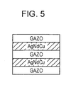
- the wavelength-selective reflective layer has a structure including at least five layers in which high refractive-index layers and metal layers are alternately laminated to each other, when a geometric film thickness L of the entire wavelength-selective reflective layer is 80 nm, a ratio ⁇ of an optical film thickness of the entire metal layers to an optical film thickness of the entire high refractive-index layers and a ratio ⁇ of an optical film thickness of a third high refractive-index layer from one of a first optical layer side and a second optical layer side to an optical film thickness of a first high refractive-index layer therefrom are included in a first region surrounded by the following formulas (1) to (4), when the geometric film thickness L of the entire wavelength-selective reflective layer is 90 nm, the ratio ⁇ and the ratio ⁇ are included in a second region surrounded by the following formulas (5) to (8), and when the geometric film thickness L of the entire wavelength-selective reflective layer is in a range of 80 to 90 nm
- an optical element including: a first optical layer having a light emission surface; a wavelength-selective reflective layer provided on the first optical layer; and a second optical layer provided on the wavelength-selective reflective layer and having a light incidence surface.
- the wavelength-selective reflective layer has a structure including at least five layers in which high refractive-index layers and metal layers are alternately laminated to each other, when a geometric film thickness L of the entire wavelength-selective reflective layer is 90 nm, a ratio ⁇ of an optical film thickness of the entire metal layers to an optical film thickness of the entire high refractive-index layers and a ratio ⁇ of an optical film thickness of a third high refractive-index layer from one of a first optical layer side and a second optical layer side to an optical film thickness of a first high refractive-index layer therefrom are included in a first region surrounded by the following formulas (5) to (8), when the geometric film thickness L of the entire wavelength-selective reflective layer is 100 nm, the ratio ⁇ and the ratio ⁇ are included in a second region surrounded by the following formulas (13) to (16), and when the geometric film thickness L of the entire wavelength-selective reflective layer is in a range of 90 to 100 nm
- an optical element including: a first optical layer having a light emission surface; a wavelength-selective reflective layer provided on the first optical layer; and a second optical layer provided on the wavelength-selective reflective layer and having a light incidence surface.
- the wavelength-selective reflective layer has a structure including at least five layers in which high refractive-index layers and metal layers are alternately laminated to each other, when a geometric film thickness L of the entire wavelength-selective reflective layer is 100 nm, a ratio ⁇ of an optical film thickness of the entire metal layers to an optical film thickness of the entire high refractive-index layers and a ratio ⁇ of an optical film thickness of a third high refractive-index layer from one of a first optical layer side and a second optical layer side to an optical film thickness of a first high refractive-index layer therefrom are included in a first region surrounded by the following formulas (13) to (16), when the geometric film thickness L of the entire wavelength-selective reflective layer is 120 nm, the ratio ⁇ and the ratio ⁇ are included in a second region surrounded by the following formulas (21) to (24), and when the geometric film thickness L of the entire wavelength-selective reflective layer is in a range of 100 to 120 nm
- an optical element including: a first optical layer having a light emission surface; a wavelength-selective reflective layer provided on the first optical layer; and a second optical layer provided on the wavelength-selective reflective layer and having a light incidence surface.
- the wavelength-selective reflective layer has a structure including at least five layers in which high refractive-index layers and metal layers are alternately laminated to each other, when a geometric film thickness L of the entire wavelength-selective reflective layer is 120 nm, a ratio ⁇ of an optical film thickness of the entire metal layers to an optical film thickness of the entire high refractive-index layers and a ratio ⁇ of an optical film thickness of a third high refractive-index layer from one of a first optical layer side and a second optical layer side to an optical film thickness of a first high refractive-index layer therefrom are included in a first region surrounded by the following formulas (21) to (24), when the geometric film thickness L of the entire wavelength-selective reflective layer is 140 nm, the ratio ⁇ and the ratio ⁇ are included in a second region surrounded by the following formulas (29) to (32), and when the geometric film thickness L of the entire wavelength-selective reflective layer is in a range of 120 to 140 n
- an optical element including: a first optical layer having a light emission surface; a wavelength-selective reflective layer provided on the first optical layer; and a second optical layer provided on the wavelength-selective reflective layer and having a light incidence surface.
- the wavelength-selective reflective layer has a structure including at least five layers in which high refractive-index layers and metal layers are alternately laminated to each other, when a geometric film thickness L of the entire wavelength-selective reflective layer is 140 nm, a ratio ⁇ of an optical film thickness of the entire metal layers to an optical film thickness of the entire high refractive-index layers and a ratio ⁇ of an optical film thickness of a third high refractive-index layer from one of a first optical layer side and a second optical layer side to an optical film thickness of a first high refractive-index layer therefrom are included in a first region surrounded by the following formulas (29) to (32), when the geometric film thickness L of the entire wavelength-selective reflective layer is 160 nm, the ratio ⁇ and the ratio ⁇ are included in a second region surrounded by the following formulas (37) to (41), and when the geometric film thickness L of the entire wavelength-selective reflective layer is in a range of 140 to 160 n
- an optical element including: a first optical layer having a light emission surface; a wavelength-selective reflective layer provided on the first optical layer; and a second optical layer provided on the wavelength-selective reflective layer and having a light incidence surface.
- the wavelength-selective reflective layer has a structure including at least five layers in which high refractive-index layers and metal layers are alternately laminated to each other, when a geometric film thickness L of the entire wavelength-selective reflective layer is 160 nm, a ratio ⁇ of an optical film thickness of the entire metal layers to an optical film thickness of the entire high refractive-index layers and a ratio ⁇ of an optical film thickness of a third high refractive-index layer from one of a first optical layer side and a second optical layer side to an optical film thickness of a first high refractive-index layer therefrom are included in a first region surrounded by the following formulas (37) to (41), when the geometric film thickness L of the entire wavelength-selective reflective layer is 180 nm, the ratio ⁇ and the ratio ⁇ are included in a second region surrounded by the following formulas (46) to (49), and when the geometric film thickness L of the entire wavelength-selective reflective layer is in a range of 160 to 180 n
- the change in color tone caused by the change in incident angle can be suppressed.
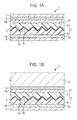
- Fig. 1A is a cross-sectional view showing one structural example of an optical film according to a first embodiment of the present invention.
- Fig. 1B is a cross-sectional view showing one example in which the optical film according to the first embodiment of the present invention is adhered to an adherend.
- An optical film 1 functioning as an optical element is an optical film having so-called directional reflection properties.
- this optical film 1 includes an optical layer 2 having a concavo-convex interface therein and a reflective layer 3 provided along the interface of this optical layer 2.
- the optical layer 2 includes a first optical layer 4 having a concavo-convex shaped first surface and a second optical layer 5 having a concavo-convex shaped second surface.
- the interface inside the optical layer 2 is formed from the first surface and the second surface, each having a concavo-convex shape, disposed so as to face each other.
- the optical film 1 includes the first optical layer 4 having a concavo-convex surface, the reflective layer 3 formed on the concavo-convex surface of the first optical layer 4, and the second optical layer 5 formed on the reflective layer 3 so as to fill the concavo-convex surface on which the reflective layer 3 is formed.
- the optical film 1 has an incident surface S1 on which sunlight or the like is incident and an emission surface S2 from which, of the light incident on this incident surface S1, light which transmits the optical film 1 is emitted.
- the optical film 1 is preferably applied to an inner wall member, an outer wall member, a window material, a wall material, and the like.
- the optical film 1 may also be preferably used as a slat (insolation shielding member) of a blind device and a screen (insolation shielding member) of a rolling screen device.
- the optical film 1 may also be preferably used as an optical element provided at a lighting portion of a fitting (interior member and/or exterior member), such as a shoji (Japanese paper shielding door).
- the optical film 1 may further includes a first base member 4a on the emission surface S2 of the optical layer 2.
- the optical film 1 may further includes a second base member 5a on the incident surface S1 of the optical layer 2.
- the optical film 1 may further include a bonding layer 6.
- This bonding layer 6 is formed on one of the incident surface S1 and the emission surface S2 of the optical film 1 which is to be adhered to a window material 10.
- the optical film 1 is adhered to the window material 10, which is an adherend, at an indoor or an outdoor side with this bonding layer 6 interposed therebetween.
- the bonding layer 6 for example, there may be used an adhesion layer (such as a UV curable resin or a two-component liquid resin) containing an adhesive as a primary component or a tacky layer (such as a pressure sensitive adhesive (PSA)) containing a tacky agent as a primary component.
- PSA pressure sensitive adhesive
- a peeling layer 7 is preferably further provided on the bonding layer 6.
- the bonding layer 6 is a tacky layer
- a peeling layer 7 is preferably further provided on the bonding layer 6. The reason for this is that by the structure as described above, when the peeling layer 7 is simply peeled off, the optical film 1 can be easily adhered to an adherend, such as the window material 10, with the bonding layer 6 interposed therebetween.
- the optical film 1 may further include a primer layer (not shown) between the second base member 5a and the bonding layer 6 and/or the second optical layer 5 in order to improve bonding properties between the second base member 5a and the bonding layer 6 and/or the second optical layer 5.
- a common physical pretreatment is preferably performed with or without using the primer layer described above.
- a plasma treatment or a corona treatment may be mentioned.
- the optical film 1 may further include a barrier layer (not shown) on the incident surface S1 or the emission surface S2 to be adhered to an adherend, such as the window material 10, or between the above surface and the reflective layer 3.
- a barrier layer (not shown) on the incident surface S1 or the emission surface S2 to be adhered to an adherend, such as the window material 10, or between the above surface and the reflective layer 3.
- the optical film 1 may further include a hard coat layer 8 in order to impart scratch resistance and the like to the surface of the optical film 1.
- This hard coat layer 8 is preferably formed on one of the incident surface S1 and the emission surface S2 of the optical film 1 opposite to that adhered to an adherend, such as the window material 10.
- a layer having water-repellent or hydrophilic properties may be further provided.
- a layer having the function as described above may be, for example, provided directly on the optical layer 2 or provided on various function layers, such as the hard coat layer 8.
- the optical film 1 preferably has flexibility since it can be easily adhered to an adherend, such as the window material 10.
- a sheet is included in the category of the film. That is, an optical sheet may also be included in the optical film 1.
- the optical film 1 has transparency.
- the transparency preferably satisfies the range of transmission image clarity which will be described later.
- the difference in refractive index between the first optical layer 4 and the second optical layer 5 is preferably 0.010 or less, more preferably 0.008 or less, and even more preferably 0.005 or less.
- the difference in refractive index is more than 0.010, the transmission image tends to blur.
- the difference in refractive index is in a range of more than 0.008 to 0.010, although depending on the outside brightness, no problems may occur in daily life.
- the difference in refractive index is in a range of more than 0.005 to 0.008, although a diffraction pattern of a very bright object, such as a light source, is disturbing, an outdoor scene can be clearly seen.
- the difference in refractive index is 0.005 or less, the diffraction pattern is hardly disturbing.
- the optical layer to be adhered to the window material 10 or the like may contain a tacky agent as a primary component.
- the optical film 1 can be adhered to the window material 10 or the like by one of the first optical layer 4 and the second optical layer 5, which contains a tacky agent as a primary component.
- the difference in refractive index of the tacky agent is preferably in the range described above.
- the first optical layer 4 preferably has the same optical properties, such as the refractive index, as those of the second optical layer 5.
- the first optical layer 4 and the second optical layer 5 are preferably formed of the same material, such as the same resin material, which has transparency in the visible region.
- the refractive indexes thereof are equal to each other, and hence, the transparency of visible light can be improved.
- the refractive indexes of the layers finally obtained may be different from each other due to curing conditions and the like in a film forming process, and hence, a careful attention is necessary.
- the refractive indexes thereof are different from each other, since the refractive indexes thereof are different from each other, light is refracted at the reflective layer 3 functioning as the border, and a transmission image tends to blur. In particular, when an object similar to a point light source, such as a distant electrical lamp, is observed, a diffraction pattern is liable to be clearly observed.
- an additive may be added to the first optical layer 4 and/or the second optical layer 5.
- the first optical layer 4 and the second optical layer 5 both preferably have transparency in the visible region.
- there are two types of definitions of the transparency that is, one definition means no light absorption and the other definition means no light scattering.
- the transparency indicates only the former; however, the optical film 1 according to the first embodiment preferably has the above two optical properties. Since a currently used retroreflector aims that reflected light reflected at a display, such as a road sign or closing of a night-time worker, can be easily viewed, even if having scattering properties, when the retroreflector is in close contact with an underlayer reflector, the reflected light reflected thereby can be viewed.
- the optical film 1 according to the first embodiment has a feature of transmitting light other than light having a specific wavelength, which is to be directionally reflected, and is adhered to a transmission object which primarily transmits light having this transmission wavelength, and the transmitted light is observed; hence, the optical film 1 preferably has no light scattering properties.
- the scattering properties may be intentionally imparted to the second optical layer 5.
- the optical film 1 is preferably used by adhesion thereof to a rigid body, such as the window material 10, having transmission properties primarily to transmitted light having a wavelength other than the specific wavelength with a tacky agent interposed therebetween.
- a rigid body such as the window material 10
- the window material 10 for example, a building window material for a high-rise building or a housing or a window material for a vehicle may be mentioned.
- the optical film 1 is particularly preferably applied to the window material 10 arranged to face any direction between the east to the west through the south (such as in any direction between the southeast to the southwest). The reason for this is that when the window material 10 is arranged at the position as described above, heat rays can be more effectively reflected.
- the optical film 1 can be used not only for a single layer window glass but also for a special glass, such as a multilayer glass.
- the window material 10 is not limited to a material formed of glass, and a polymer material having transparency may also be used.
- the optical layer 2 preferably has transparency in the visible region. The reason for this is that since the optical layer 2 has transparency as described above, when the optical film 1 is adhered to the window material 10, such as a window glass, visible light can be transmitted, and lighting by sunlight can be ensured.
- the surface to be adhered besides an inside surface of the glass, an outside surface thereof may also be used.
- the optical film 1 may be used together with another heat ray shielding film, and for example, an optical absorption coating film may also be provided at the interface between air and the optical film 1 (that is, on the outermost surface of the optical film 1).
- the optical film 1 may also be used together with a hard coat layer, an ultraviolet protection layer, a surface antireflective layer, and the like.
- these functional layers are preferably provided at the interface between the optical film 1 and air.
- an ultraviolet protection layer is necessarily arranged closer to a sun side than the optical film 1, in particular, when the optical film 1 is used on a window glass surface at an indoor side, the ultraviolet protection layer is preferably provided between this window glass surface and the optical film 1.
- an ultraviolet absorber may also be kneaded in a bonding layer provided between the window glass surface and the optical film 1.
- the optical film 1 may be colored in order to impart design characteristics thereto.
- the design characteristics are imparted as described above, at least one of the first the optical layer 4 and the second optical layer 5 is preferably formed to primarily absorb light in a specific wavelength band in the visible region without degrading the transparency.
- Fig. 2 is a perspective view showing the relationship between incident light incident on the optical film 1 and reflected light reflected by the optical film 1.
- the optical film 1 has an incident surface S1 on which light L is incident. It is preferable that of the light L incident on the incident surface S1 at an incident angle ( ⁇ , ⁇ ), the optical film 1 selectively directionally reflects light L 1 in a specific wavelength band in a direction other than a specular reflection direction (- ⁇ , ⁇ +180°) while transmitting light L 2 other than that in the specific wavelength band.
- the optical film 1 has transparency to the light other than that in the specific wavelength band. As the transparency, the transmission image clarity is preferably in the range which will be described later.
- ⁇ indicates an angle formed between a normal l 1 to the incident surface S1 and the incident light L or the reflected light L 1 .
- ⁇ indicates an angle formed between a specific straight line l 2 within the incident surface S1 and a component of the incident light L or the reflected light L 1 projected on the incident surface S1.
- the specific straight line l 2 within the incident surface is an axis at which the reflection intensity in a ⁇ direction is maximized when the incident angle ( ⁇ , ⁇ ) is fixed, and the optical film 1 is rotated around the normal l 1 to the incident surface S1 thereof (see Figs. 3A to 4B ).
- an angle ⁇ rotated clockwise around the normal l 1 is represented by "+ ⁇ ”
- an angle ⁇ rotated anticlockwise is represented by "- ⁇ .”
- An angle ⁇ rotated clockwise around the straight line l 2 is represented by "+ ⁇ ”
- an angle ⁇ rotated anticlockwise is represented by "- ⁇ ”.
- the light in the specific wavelength band which is selectively directionally reflected and the specific light to be transmitted are changed depending on the application of the optical film 1.
- the light in the specific wavelength band which is selectively dimensionally reflected is preferably near-infrared light
- the specific wavelength to be transmitted is preferably visible light.
- the light in the specific wavelength band which is selectively dimensionally reflected is preferably near-infrared light having a primary wavelength band of 780 to 2,100 nm.
- the directional reflection indicates reflection in a specific direction other than the specular reflection, and the intensity of the directional reflection is sufficiently higher than the intensity of the diffuse reflection which has no directivity.
- the reflection indicates that the reflectance in a specific wavelength band, for example, in the near-infrared region, is preferably 30% or more, more preferably 50% or more, and even more preferably 80% or more.
- the transmission indicates that the transmittance in a specific wavelength band region, for example, in the visible region, is preferably 30% or more, more preferably 50% or more, and even more preferably 70% or more.
- a directional reflection direction ⁇ o is preferably in a range of -90° to 90°.
- the reason for this is that when the optical film 1 is adhered to the window material 10, of light coming from the sky, light in a specific wavelength band can be returned in a skyward direction. When there are no high-rise buildings in the vicinity, the optical film 1 in this range is effective.
- the directional reflection direction is preferably in the vicinity of ( ⁇ , - ⁇ ). The vicinity indicates preferably within 5° from ( ⁇ , - ⁇ ), more preferably within 3°, and even more preferably within 2°.
- a three-dimensional structure such as a part of a sphere, a part of a hyperbola, a triangular pyramid, a quadrangular pyramid, or a cone, is preferably used.
- Light incident in a ( ⁇ , ⁇ ) direction (-90° ⁇ 90°) can be reflected in accordance with the shape in a ( ⁇ o, ⁇ o) direction (0° ⁇ o ⁇ 90°,-90° ⁇ o ⁇ 90°).
- a columnar body extended in one direction is preferable.
- Light incident in a ( ⁇ , ⁇ ) direction (-90° ⁇ 90°) can be reflected in accordance with the inclined angle of the columnar shape in a ( ⁇ o, - ⁇ ) direction (0° ⁇ o ⁇ 90°).
- the directional reflection of light in a specific wavelength band is preferably in the vicinity of retroreflection, that is, the reflection direction of light in a specific wavelength band with respect to the light incident on the incident surface S1 at an incident angle ( ⁇ , ⁇ ) is preferably in the vicinity of ( ⁇ , ⁇ ).
- the reason for this is that when the optical film 1 is adhered to the window material 10, of light coming from the sky, light in a specific wavelength band can be returned skyward.
- the vicinity is preferably within 5°, more preferably within 3°, and even more preferably within 2°.
- the reason for this is that when the reflection direction is within the range described above, and the optical film 1 is adhered to the window material 10, of light coming from the sky, light in a specific wavelength band can be efficiently returned skyward.
- the retroreflection direction is necessarily equal to the incident direction; however, when sensing is not necessarily performed in a specific direction as in the case of the present invention, the retroreflection direction may not be strictly made equal to the incident direction.
- the value of the transmission image clarity measured using an optical comb with a width of 0.5 mm in a wavelength band having transmission properties is preferably 50 or more, more preferably 60 or more, and even more preferably 75 or more.
- the transmission image clarity is less than 50, the transmission image tends to blur.
- the value is in a range of 50 to less than 60, although depending on the outside brightness, no problems may occur in daily life.
- the value is in a range of 60 to less than 75, although a diffraction pattern of a very bright object, such as a light source, is disturbing, an outdoor scene can be clearly seen.
- the value is 75 or more, the diffraction pattern is hardly disturbing.
- the total value of the transmission image clarity measured using an optical comb with a width of 0.125 mm, 0.5 mm, 1.0 mm, and 2.0 mm is preferably 230 or more, more preferably 270 or more, and even more preferably 350 or more.
- the transmission image clarity is less than 230, the transmission image tends to blur.
- the total value is in a range of 230 to less than 270, although depending on the outside brightness, no problems may occur in daily life.
- the total value is in a range of 270 to less than 350, although a diffraction pattern of a very bright object, such as a light source, is disturbing, an outdoor scene can be clearly seen.
- the total value is 350 or more, the diffraction pattern is hardly disturbing.
- the value of the transmission image clarity is measured in accordance with JIS K7105 using ICM-1T manufactured by Suga Test Instruments Co., Ltd.
- measurement is preferably performed after correction is performed using a filter for the wavelength to be desirably transmitted.
- a haze in a wavelength band having transmission properties is preferably 6% or less, more preferably 4% or less, and even more preferably 2% or less.
- the reason for this is that when the haze is more than 6%, transmitted light is scattered and blurred.
- the haze is measured in accordance with a measuring method specified by JIS K7136 using HM-150 manufactured by Murakami Color Research Laboratory Co., Ltd.
- measurement is preferably performed after correction is performed using a filter for the wavelength to be desirably transmitted.
- the incident surface S1 of the optical film 1 has a smoothness so as not to degrade the transmission image clarity, and preferably, the incident surface S1 and the emission surface S2 both have the smoothness as described above.
- an arithmetic average roughness Ra of each of the incident surface S1 and the emission surface S2 is preferably 0.08 ⁇ m or less, more preferably 0.06 ⁇ m or less, and even more preferably 0.04 ⁇ m or less.
- the arithmetic average roughness Ra described above is calculated as a roughness parameter by measuring the surface roughness of the incident surface and obtaining a roughness curve from a two-dimensional profile curve.
- the measurement conditions are set in accordance with JIS B0601: 2001. A measurement apparatus and measurement conditions are shown below.
- Measurement apparatus full automatic microprofile-measuring instrument Surfcorder ET4000A (manufactured by Kosaka Laboratory Ltd.)
- ⁇ c is set to 0.8 mm; an evaluation length is set to 4 mm; a cutoff is set to 5 times; and a data sampling interval is set to 0.5 ⁇ m.
- the transmission color of the optical film 1 is preferably as neutral as possible and, even if being colored, the transmission color preferably has a light color tone that appears cool, such as blue, blue-green, or green.
- the chromaticity coordinates x and y of the transmitted light incident on the incident surface S1, passing through the optical layer 2 and the reflective layer 3, and radiating from the emission surface S2, and the chromaticity coordinates x and y of the reflected light preferably satisfy, for example, 0.20 ⁇ x ⁇ 0.35 and 0.20 ⁇ y ⁇ 0.40, more preferably 0.25 ⁇ x ⁇ 0.32 and 0.25 ⁇ y ⁇ 0.37, and even more preferably 0.30 ⁇ x ⁇ 0.32 and 0.30 ⁇ y ⁇ 0.35 in the case of illumination of the D65 light source.
- y>x-0.02 is preferably satisfied, and y>x is more preferably satisfied.
- y>x is more preferably satisfied.
- the absolute value of the difference in the chromaticity coordinate x of light incident on the incident surface S1 or the emission surface S2 at an incident angle ⁇ in a range of 5° to 60° and specularly reflected by the optical film 1 and the absolute value of the difference in the chromaticity coordinate y of the light are each preferably 0.05 or less, more preferably 0.03 or less, and even more preferably 0.01 or less at each primary surface of the optical film 1.
- the above numerical limitations of the chromaticity coordinates x and y of the reflected light are preferably satisfied for both the incident surface S1 and the emission surface S2.
- the first optical layer 4, the second optical layer 5, and the reflective layer 3, which form the optical film 1, will be sequentially described.
- the first optical layer 4 is a layer, for example, to support and protect the reflective layer 3. Since imparting flexibility to the optical film 1, the first optical layer 4 is formed of, for example, a layer containing a resin as a primary component. For example, one of the two primary surfaces of the first optical layer 4 is a smooth surface, and the other surface is a concavo-convex surface (a first surface). The reflective layer 3 is formed on this concavo-convex surface.
- the second optical layer 5 is a layer to protect the reflective layer 3 by embedding the first surface (concavo-convex surface) of the first optical layer 4 on which the reflective layer 3 is formed.
- the second optical layer 5 is formed, for example, of a layer containing a resin as a primary component.
- one of the two primary surfaces of the second optical layer 5 is a smooth surface, and the other surface is a concavo-convex surface (a second surface).
- the concavo-convex surface of the first optical layer 4 and the concavo-convex surface of the second optical layer 5 have the relationship in which the concavo-convex shapes are reversed to each other.
- the concavo-convex surface of the first optical layer 4 is formed, for example, of at least two structures 4c which are one-dimensionally arranged.
- the concavo-convex surface of the second optical layer 5 is formed, for example, of at least two structures 5c which are one-dimensionally arranged (see Figs. 3A to 4B ). Since the structure 4c of the first optical layer 4 and the structure 5c of the second optical layer 5 are only different from each other such that the concavo-convex shapes thereof are reversed, hereinafter, the structure 4c of the first optical layer 4 will be described.
- the pitch P of the structures 4c is preferably in a range of 5 ⁇ m to 5 mm, more preferably in a range of 5 ⁇ m to less than 250 ⁇ m, and even more preferably in a range of 20 to 200 ⁇ m.
- the pitch of the structures 4c is less than 5 ⁇ m, it is difficult to form a desired shape thereof, and in addition, it is also generally difficult to obtain steep wavelength selection properties of the reflective layer 3; hence, the transmission wavelength may be partially reflected in some cases.
- the reflection as described above occurs, since diffraction is generated, and high-order reflection is also viewed, the transparency tends to look not so good.
- the pitch of the structures 4c is more than 5 mm, when the shape of the structure 4c necessary for the directional reflection is taken into consideration, a necessary film thickness becomes large, the flexibility is lost, and as a result, it becomes difficult to adhere the optical film 1 to a rigid body, such as the window material 10.
- the pitch of the structures 4c is set to less than 250 ⁇ m, since the flexibility is further increased, a roll-to-roll manufacturing process can be easily performed, and a batch manufacturing process may not be necessary.
- the optical film 1 is necessary to have a length of approximately several meters, and hence, a roll-to-roll manufacturing process is suitably performed rather than a batch manufacturing process. Furthermore, when the pitch is set in a range of 20 to 200 ⁇ m, the productivity is further improved.
- the shape of the structure 4c formed in the surface of the first optical layer 4 is not limited to one type, and the structures 4c may be formed in the surface of the first optical layer 4 to have at least two types of shapes.
- the structures 4c having at least two types of shapes are formed in the surface, a predetermined pattern formed of the structures 4c having at least two types of shapes may be periodically repeated.
- the structures 4c having at least two types of shapes may be randomly formed (aperiodically).
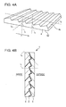
- Figs. 3A to 3C are perspective views each showing a shape example of the structure formed in the first optical layer.
- the structures 4c are each a columnar concave portion extended in one direction and are one-dimensionally arranged in one direction. Since being formed on the structures 4c, the reflective layer 3 has the same shape as the surface shape of the structures 4c.
- the shape of the structure 4c for example, there may be mentioned a prism shape shown in Fig. 3A , a shape having a round ridgeline portion of a prism shown in Fig. 3B , a reversed shape of a lenticular shape in Fig. 3C , or a reversed shape thereof.
- the lenticular shape indicates a shape in which the cross-section perpendicular to a ridgeline of the convex portion is a part of an arc shape or an almost arc shape, an elliptical arc shape or an almost elliptical arc shape, or a parabolic shape or an almost parabolic shape. Therefore, a cylindrical shape is also categorized in the lenticular shape.
- a round shape (R) may be formed at the ridgeline portion, and the ratio R/P, that is, the ratio of a curvature radius R to the pitch P of the structure 4c is preferably 7% or less, more preferably 5% or less, and even more preferably 3% or less.
- the shape of the structure 4c is not limited to the shapes shown in Figs. 3A to 3C and the reversed shapes thereof, and a toroidal shape, a hyperbolic columnar shape, an elliptical columnar shape, a polygonal columnar shape, and a free-form shape may also be used.
- the vertex of the prism shape or the lenticular shape may be formed to have a polygonal shape (such as a pentagonal shape).
- an inclined angle ⁇ of the prism-shaped structure 4c is 45° or the like.
- the structure 4c preferably has a flat surface or a curved surface having an inclined angle of 45° or more in order to return light coming from the sky in a skyward direction as much as possible by reflection.
- the reason the shape as described above is formed is that since the incident light is almost returned skyward by one reflection, even if the reflectance of the reflective layer 3 is not so high, the incident light can be efficiently reflected in a skyward direction, and light absorption in the reflective layer 3 can also be reduced.
- the structure 4c may have an asymmetric shape with respect to the normal l 1 to the incident surface S1 or the emission surface S2 of the optical film 1.
- a primary axis l m of the structure 4c is inclined in an arrangement direction a of the structure 4c with respect to the normal l 1 .
- the primary axis l m of the structure 4c indicates a straight line passing through a central point of the base of a cross-section of the structure 4c and the vertex thereof.
- the primary axis l m of the structure 4c is preferably inclined to a lower side (ground side) of the window material 10 with respect to the normal l 1 .
- the reason for this is that in general, since a larger amount of heat enters through a window about in early afternoon, and the height of the sun is larger than an angle of 45° in many cases, by using the shape described above, light incident at these high angles as described above can be efficiently reflected upward.
- An asymmetrical prism shape of the structure 4c with respect to the normal l 1 is shown by way of example in Figs. 4A and 4B .
- the structure 4c having a shape other than a prism shape may also have an asymmetrical shape with respect to the normal l 1 .
- a corner cube body may have an asymmetric shape with respect to the normal I1.
- the first optical layer 4 preferably includes a resin as a primary component in which a decrease in storage modulus at 100°C is small and in which the storage modulus at 25°C is not considerably different from that at 100°C.
- a resin having a storage modulus of 3 ⁇ 10 9 Pa or less at 25°C and a storage modulus of 3 ⁇ 10 7 Pa or more at 100°C is preferably contained.
- the first optical layer 4 may include at least two types of resins.
- at least one additive may be contained.
- a designed interface shape can be mostly maintained.
- a resin is used as a primary component in which a decrease in storage modulus at 100°C is small and the storage modulus at 25°C and that at 100°C are not so much different from each other, even when a process including heating with or without pressure application is performed after the formation of the concavo-convex surface (the first surface) of the first optical layer 4, a designed interface shape can be mostly maintained.
- a resin is used as a primary component in which a decrease in storage modulus at 100°C is large and the storage modulus at 25°C and that at 100°C are significantly different from each other, a designed interface shape is considerably deformed, and for example, the optical film 1 may be curled in some cases.
- the process including heating besides a process, such as an annealing treatment, in which heat is directly applied to the optical film 1 or constituent members thereof, for example, there may be mentioned a process in which when a thin film is formed or a resin composition is cured, the temperature of a film forming surface is locally increased and is indirectly applied to the thin film or the resin composition and a process in which the temperature of a mold is increased by energy ray radiation and is indirectly applied to an optical film.
- the effect obtained by limiting the numerical value range of the storage modulus described above is not particularly limited to a specific type of resin and can be obtained from any type of a thermoplastic resin, a thermosetting resin, and an energy ray curable resin.
- the storage modulus of the first optical layer 4 can be confirmed, for example, as described below.
- the storage modulus of its exposed surface can be confirmed by measurement using a microhardness tester.
- the first base member 4a or the like is formed on the surface of the first optical layer 4, after the first base member 4a or the like is peeled off to expose the surface of the first optical layer 4, the storage modulus of the exposed surface can be confirmed by measurement using a microhardness tester.
- thermoplastic resin for example, a method for adjusting the length of a side chain or the type thereof may be mentioned, and in the case of a thermosetting resin and an energy ray curable resin, for example, a method for adjusting the number of cross-linking points and the molecular structure of a cross-linking agent may be mentioned.
- thermosetting resin and an energy ray curable resin for example, a method for adjusting the number of cross-linking points and the molecular structure of a cross-linking agent may be mentioned.
- a method for adjusting the number of cross-linking points and the molecular structure of a cross-linking agent may be mentioned.
- it is preferable that necessary performance of a resin material itself is not degraded by the structural change as describe.
- a resin may become fragile since the modulus thereof at approximately room temperature is increased, and a film may be warped or curled since the shrinkage thereof is increased; hence, the type of cross-linking agent is appropriately selected in accordance with desired properties.
- the first optical layer 4 includes a crystalline polymer material as a primary component
- a resin is preferably used as a primary component in which the glass transition point is higher than the highest temperature in a manufacturing process and a decrease in storage modulus at the highest temperature in the manufacturing process is small.
- a resin is used in which the glass transition point is in a range of a room temperature of 25°C to the highest temperature in a manufacturing process and a decrease in storage modulus at the highest temperature in the manufacturing process is large, it becomes difficult to maintain a designed ideal interface shape in the manufacturing process.
- the first optical layer 4 includes an amorphous polymer material as a primary component
- a resin is preferably used as a primary component in which the melting point is higher than the highest temperature in a manufacturing process and a decrease in storage modulus at the highest temperature in the manufacturing process is small.
- a resin is used in which the melting point is in a range of a room temperature of 25°C to the highest temperature in a manufacturing process and a decrease in storage modulus at the highest temperature in the manufacturing process is large, a designed ideal interface shape may be difficult to be maintained in the manufacturing process.
- the highest temperature in a manufacturing process indicates the highest temperature of the concavo-convex surface (the first surface) of the first optical layer 4 in the manufacturing process. It is preferable when the second optical layer 5 also satisfies the numerical value range of the storage modulus and the temperature range of the glass transition point described above.
- At least one of the first optical layer 4 and the second optical layer 5 preferably contains a resin having a storage modulus of 3 ⁇ 10 9 Pa or less at 25°C.
- the reason for this is that since the flexibility can be imparted to the optical film 1 at a room temperature of 25°C, the optical film 1 can be manufactured by a roll-to-roll manufacturing method.
- the first base member 4a and the second base member 5a have, for example, transparency.
- the base member preferably has a film shape in order to impart flexibility to the optical film 1, the base member is not particularly limited to this shape.
- a material for the first base member 4a and the second base member 5a for example, a common polymer material may be used.
- the common polymer material for example, there may be mentioned a triacetyl cellulose (TAC), a polyester (TPEE), a poly(ethylene terephthalate) (PET), a polyimide (PI), a polyamide (PA), an aramid, a polyethylene (PE), a polyacrylate, a polyethersulfone, a polysulfone, a polypropylene (PP), a diacetyl cellulose, a poly(vinyl chloride), an acryl resin (PMMA), a polycarbonate (PC), an epoxy resin, a urea resin, a urethane resin, or a melamine resin; however, the polymer material is not particularly limited to the above materials.
- the thickness of the first base member 4a and that of the second base member 5a are each preferably in a range of 38 to 100 ⁇ m; however, the thickness is not limited thereto.
- the first base member 4a and the second base member 5a each preferably have energy ray transparency. The reason for this is that as describe below, an energy ray curable resin provided between the reflective layer 3 and the first base member 4a or the second base member 5a can be cured by irradiation of energy rays from the first base member 4a or the second base member 5a side.
- the first optical layer 4 and the second optical layer 5 have, for example, transparency.
- the first optical layer 4 and the second optical layer 5 can be obtained, for example, by curing a resin composition.
- a resin composition in view of the ease of manufacture, an energy ray curable resin to be cured by light, electron rays, or the like or a thermosetting resin to be cured by heat is preferably used.
- the energy ray curable resin a photosensitive resin composition to be cured by light is preferable, and an ultraviolet curable resin composition to be cured by ultraviolet light is most preferable.
- the resin composition preferably further contains a compound containing phosphoric acid, a compound containing succinic acid, and/or a compound containing butyrolactone.
- a compound containing phosphoric acid for example, a (meth)acrylate containing phosphoric acid may be used, and a (meth)acrylic monomer containing phosphoric acid as a functional group or an oligomer thereof may be preferably used.
- the compound containing succinic acid for example, a (meth)acrylate containing succinic acid may be used, and a (meth)acrylic monomer containing succinic acid as a functional group or an oligomer thereof may be preferably used.
- a (meth)acrylate containing succinic acid for example, a (meth)acrylate containing succinic acid may be used, and a (meth)acrylic monomer containing butyrolactone as a functional group or an oligomer thereof may be preferably used.
- the ultraviolet curable resin composition contains, for example, a (meth)acrylate and a photopolymerization initiator.
- the ultraviolet curable resin composition may further contain a light stabilizer, a flame retarder, a leveling agent, an antioxidant, and the like.
- the acrylate a monomer having at least two (meth)acryloyl groups and/or an oligomer thereof is preferably used.
- this monomer and/or the oligomer thereof for example, a urethane (meth)acrylate, an epoxy (meth)acrylate, a polyester (meth)acrylate, a polyol (meth)acrylate, a polyether (meth)acrylate, or a melamine (meth)acrylate may be used.
- the (meth)acryloyl group indicates one of an acryloyl group and a methacryloyl group.
- the oligomer indicates a molecule having a molecular weight in a range of 500 to 60,000.
- the photopolymerization initiator a compound appropriately selected from common materials may be used.
- the common material for example, a benzophenone derivative, an acetophenone derivative, and an anthraquinone derivative may be used alone or in combination.
- the amount of the polymerization initiator is preferably in a range of 0.1 to 10 percent by mass in a solid content. When the amount is less than 0.1 percent by mass, photocurability is degraded, and practical industrial production may not be suitably performed. On the other hand, when the amount of the polymerization initiator is more than 10 percent by mass, and the amount of irradiation light is small, an odor tends to remain in a coating film.
- the solid content indicates all the components forming a cured hard coat layer.
- an acrylate, a photopolymerization initiator, and the like are collectively called the solid content.
- a resin to which the structure can be transferred by energy ray irradiation, heat, and the like is preferably used, and as long as the above-described request for the refractive index is satisfied, any type of resin, for example, a heat curable resin or an ionizing radiation curable resin, such as an epoxy resin, or a thermoplastic resin, such as polycarbonate or polyacrylate, may be used.
- a heat curable resin or an ionizing radiation curable resin such as an epoxy resin
- a thermoplastic resin such as polycarbonate or polyacrylate
- An oligomer may be added in order to decrease the curing shrinkage.
- a polyisocyanate or the like may also be included as a curing agent.
- at least one of a monomer having a hydroxyl group, a carboxyl group, or a phosphoric group; a polyalcohol compound; a carboxylic acid; a silane, an aluminum or a titanium coupling agent; and various chelating agents may also be added.
- the resin composition preferably further contains a cross-linking agent.
- a cross-linking agent in particular, a cyclic cross-linking agent is preferably used. The reason for this is that by using a cross-linking agent, heat resistance can be imparted to the resin without considerably changing the storage modulus at room temperature. If the storage modulus at room temperature considerably changes, the optical film 1 will become fragile, and production of the optical film 1 by a roll-to-roll process or the like becomes difficult.
- cyclic cross-linking agent for example, there may be mentioned dioxane glycol diacrylate, tricyclodecane dimethanol diacrylate, tricyclodecane dimethanol dimethacrylate, ethylene oxide-modified isocyanuric acid diacrylate, ethylene oxide-modified isocyanuric acid triacrylate, or caprolactone-modified tris(acryloxyethyl) isocyanurate.
- the first base member 4a or the second base member 5a preferably has a lower water vapor transmission rate than that of the first optical layer 4 or the second optical layer 5.
- the first base member 4a is preferably formed, for example, of a poly(ethylene terephthalate) (PET) having energy ray transmission properties and a lower water vapor transmission rate than that of the first optical layer 4.
- PET poly(ethylene terephthalate)
- the water vapor transmission rate of a PET having a thickness of 75 ⁇ m is approximately 10 g/m2 /day (40°C, 90% RH).
- the first optical layer 4 and the second optical layer 5 includes a functional group having high polarity, and that the content thereof in the first optical layer 4 is different from that in the second optical layer 5. It is preferable that the first optical layer 4 and the second optical layer 5 both contain a phosphoric acid compound, (such as a phosphoric ester), and that the content thereof in the first optical layer 4 is different from that in the second optical layer 5.
- the content of a phosphoric acid compound in the first optical layer 4 is preferably different from that in the second optical layer 5 by two times or more, more preferably 5 times or more, and even more preferably by 10 times or more.
- the reflective layer 3 preferably contains an oxide, a nitride, or an oxynitride in a surface thereof which is in contact with at least one of the first optical layer 4 and the second optical layer 5 which contains a phosphoric acid compound.
- the reflective layer 3 preferably has a layer containing zinc oxide (ZnO) or a niobium oxide which is in contact with at least one of the first optical layer 4 and the second optical layer 5 which contains a phosphoric acid compound. The reason for this is to improve the adhesion between at least one of these optical layers and the reflective layer 3.
- the reason for this is that when the reflective layer 3 contains a metal, such as Ag, a high corrosion resistance effect can be obtained.
- the reflective layer 3 may also contain a dopant, such as Al or Ga. The reason for this is that when a metal oxide layer is formed by a sputtering method or the like, the film quality and the smoothness are improved.
- At least one of the first optical layer 4 and the second optical layer 5 preferably has properties of absorbing light in a specific wavelength band in the visible region.
- a pigment to be dispersed in the resin may be any one of an organic-based pigment and an inorganic-based pigment, in particular, an inorganic pigment having inherent high weather resistance is preferably used.
- inorganic pigments such as zircon gray (Co, Ni-doped ZrSiO 4 ) praseodymium yellow (Pr-doped ZrSiO 4 ) chromium titanium yellow (Cr, Sb-doped TiO 2 or Cr, W-doped TiO 2 ), chrome green (such as Cr 2 O 3 ), peacock blue ((CoZn)O(AlCr) 2 O 3 ), Victoria green (Al, Cr) 2 O 3 ), dark blue (CoO-Al 2 O 3 -SiO 2 ), banadium zirconium blue (V-doped ZrSiO 4 ) chrome tin pink (Cr-doped CaO-SnO 2 -SiO 2 ), manganese pink (Mn-doped Al 2 O 3 ), and salmon pink (Fe-doped ZrSiO 4 ); and organic pigments, such as an azo pigment and a
- the reflective layer is a wavelength-selective reflective layer formed of a laminated film in which, of light incident on an incident surface at an incident angle ( ⁇ , ⁇ ), light in a specific wavelength band is directionally reflected while light other than that in the specific wavelength band is allowed to pass therethrough.
- the average thickness of the reflective layer 3 is preferably 20 ⁇ m or less, more preferably 5 ⁇ m or less, and even more preferably 1 ⁇ m or less. When the average thickness of the reflective layer 3 is more than 20 ⁇ m, the length of a light path in which transmitted light is refracted is increased, and a transmission image is liable to look distorted.
- a formation method of the reflective layer for example, a sputtering method, a deposition method, a dip coating method, and a die coating method may be mentioned.
- the laminated film is a laminated film having at least five layers, for example, in which metal layers having a high reflectance in the infrared region and high refractive-index layers having a high refractive index to the metal film in the visible region and functioning as an antireflective layer are alternately laminated to each other.
- the high refractive-index layer an optically transparent layer or a transparent conductive layer may be used.
- the metal layer having a high reflectance in the infrared region contains, for example, as a primary component an element, such as Au, Ag, Cu, Al, Ni, Cr, Ti, Pd, Co, Si, Ta, W, Mo, or Ge, or an alloy containing at least two elements mentioned above.
- an element such as Au, Ag, Cu, Al, Ni, Cr, Ti, Pd, Co, Si, Ta, W, Mo, or Ge, or an alloy containing at least two elements mentioned above.
- a Ag-based, a Cu-bases, an Al-based, a Si-based, or a Ge-based material is preferably used.
- the metal layer When an alloy is used as a material for the metal layer, the metal layer preferably contains AlCu, AlTi, AlCr, AlCo, AlNdCu, AlMgSi, AgBi, AgNdCu, AgPdCu, AgPdTi, AgCuTi, AgPdCa, AgPdMg, AgPdFe, Ag, or SiB as a primary component.
- a material such as Ti or Nd, is preferably added thereto.
- the material mentioned above is preferably added.
- the optically transparent layer is an optically transparent layer which has a high refractive index in the visible region and functions as an antireflective layer.
- the optically transparent layer contains, for example, a high dielectric material, such as niobium oxide, tantalum oxide, or titanium oxide, as a primary component.
- the transparent conductive layer contains, for example, as a primary component a ZnO-based oxide or an indium-doped tin oxide.
- ZnO-based oxide for example, at least one selected from the group consisting of zinc oxide (ZnO), gallium (Ga) and aluminum (Al)-doped zinc oxide (GAZO), Al-doped zinc oxide (AZO), and gallium (Ga)-doped zinc oxide (GZO) may be used.
- the refractive index of the high refractive-index layer included in the laminated film is preferably in a range of 1.7 to 2.6.
- the refractive index is more preferably in a range of 1.8 to 2.6 and even more preferably in a range of 1.9 to 2.6.
- the refractive index is at a wavelength of 550 nm.
- the high refractive-index layer is a layer containing, for example, a metal oxide as a primary component.
- a metal oxide other than zinc oxide may be preferably used in some cases.
- at least one selected from the group consisting of niobium oxide (such as niobium pentoxide), tantalum oxide (such as tantalum pentoxide), and titanium oxide is preferably used.
- the film thickness of the high refractive-index layer is preferably in a range of 10 to 120 nm, more preferably in a range of 10 to 100 nm, and even more preferably in a range of 10 to 80 nm. When the film thickness is less than 10 nm, visible light tends to be easily reflected. On the other hand, when the thickness is more than 120 nm, a decrease in transmittance and the generation of cracks are liable to occur.
- Fig. 5 shows one example of the lamination structure of the reflective layer 3.
- Layers of the reflective layer 3 are called a first, a second, a third, a fourth, and a fifth layer from the emission surface side and will be described below.
- the first layer, the third layer, and the fifth layer are each a high refractive-index layer containing, for example, GAZO as a primary component, and the film thickness of the first layer is formed approximately equal to that of the fifth layer.
- the difference in film thickness between the first layer and the fifth layer is preferably 10% or less with respect to the film thickness of one of the two layers, more preferably 5% or less, and even more preferably 3% or less.
- the second layer and the fourth layer are each a metal layer formed, for example, of AgNdCu as a primary component, and the film thicknesses thereof are formed approximately equal to each other.
- the difference in film thickness between the second layer and the fourth layer is preferably 10% or less with respect to the film thickness of one of the two layers, more preferably 5% or less, and even more preferably 3% or less.
- the lamination structure of the reflective layer 3 is not limited thereto, and for example, a plurality of separated layers may form one high refractive-index layer.
- Figs. 6A to 6F each show one example of the lamination structure of the reflective layer 3 in which a plurality of separated layers forms one high refractive index layer.
- the third and the fifth high refractive-index layers are each formed of two layers respectively containing ZnO and Nb 2 O 5 as a primary component.
- Fig. 6A the third and the fifth high refractive-index layers are each formed of two layers respectively containing ZnO and Nb 2 O 5 as a primary component.
- the third high refractive-index layer is formed of three layers respectively containing GAZO, Nb 2 O 5 , and GAZO as a primary component
- the fifth high refractive-index layer is formed of two layers respectively containing GAZO and Nb 2 O 5 as a primary component
- the third high refractive-index layer is formed of two layers respectively containing ZnO and Nb 2 O 5 as a primary component
- the fifth high refractive-index layer is formed of three layers respectively containing ZnO, Nb 2 O 5 , ZnO as a primary component.
- the first, the third, and the fifth high refractive-index layers are each formed of two layers respectively containing GAZO and Nb 2 O 5 as a primary component.
- the first and the fifth high refractive-index layers are each formed of two layers respectively containing GAZO and Nb 2 O 5 as a primary component
- the third high refractive-index layer is formed of three layers respectively containing GAZO, Nb 2 O 5 , and GAZO as a primary component.
- the first high refractive-index layer is formed of two layers respectively containing GAZO and Nb 2 O 5 as a primary component
- the third and the fifth high refractive-index layers are each formed of three layers respectively containing GAZO, Nb 2 O 5 , and GAZO as a primary component.
- the laminated film is not limited to a thin film formed of an inorganic material and may be formed by laminating thin films formed of a polymer material or layers containing a polymer material and fine particles dispersed therein.
- a buffer layer of Ti or the like having a small thickness, such as approximately several nanometers, may be provided at an interface of the optically transparent layers.
- the buffer layer is a layer which oxidizes itself in the formation of the upper layer so as to suppress the oxidation of the metal layer or the like functioning as an underlayer.
- an index value which indicates the color tone such as blueness or redness
- the change in color tone is suppressed by forming a laminated film so as to satisfy this index value.
- a blueness index and a redness index are each set as the index value for the color tone.
- the blueness index is an index value to judge whether transmitted light has blueness or not.
- a blueness index value is calculated in such a way that after a product of a light source spectrum in a wavelength range of 620 to 750 nm, reflectance, and luminosity factor is integrated, and the value obtained thereby is divided by a value obtained by integrating a product of the light source spectrum and the luminosity factor.
- the blueness index value is preferably less than 0.152 and more preferably less than 0.111.
- the reason for this is that when the blueness index value is in a range of 0 to less than 0.111, the blueness is hardly disturbing, and when it is in a range of 0.111 to less than 0.152, although depending on the outside brightness, the blueness is almost not disturbing.
- the blueness index value is in a range of 0.152 to less than 0.2, transmitted light is liable to have a slight blueness in a specific angle direction, and when it is 0.2 or more, transmitted light is liable to have a deep blueness in a specific angle direction.
- the redness index is an index value to judge whether transmitted light has redness or not.
- the redness index value is calculated in such a way that after a product of a light source spectrum in a wavelength range of 620 to 750 nm, reflectance, and luminosity factor is integrated, and the value obtained thereby is divided by a value obtained by integrating a product of the light source spectrum and the luminosity factor.
- the redness index value is preferably less than 0.258 and more preferably less than 0.175.
- the reason for this is that when the redness index value is in a range of 0 to less than 0.175, the redness is hardly disturbing, and when it is in a range of 0.175 to less than 0.258, although depending on the outside brightness, the redness is almost not disturbing.
- the redness index value is in a range of 0.258 to less than 0.3, transmitted light is liable to have a slight redness in a specific angle direction, and when it is 0.3 or more, transmitted light is liable to have a deep redness in a specific angle direction.
- Figs. 7A and 7B are cross-sectional views each illustrating one example of the function of an optical film.
- the structure has a prism shape of an inclined angle of 45° will be described by way of example.
- Fig. 7A although some of near-infrared light L 1 of sunlight incident on this optical film 1 is directionally reflected skyward in a direction approximately equivalent to the incident direction, visible light L 2 transmits the optical film 1.
- the light incident on the optical film 1 and reflected on the reflective layer surface of the reflective layer 3 is separated into a component L A reflected skyward and a component L B not reflected skyward at a ratio in accordance with the incident angle.
- the component L B not reflected skyward is finally reflected in a direction different from the incident direction.
- the ratio of the component L B not reflected skyward increases, the ratio of the incident light reflected skyward will decrease.
- appropriate designing of the shape of the reflective layer 3 that is, appropriate designing of the shape of the structure 4c of the first optical layer 4 is effective.
- the shape of the structure 4c preferably has the lenticular shape shown in Fig. 3C or the asymmetrical shape shown in Figs. 4A and 4B .
- the two shapes shown in Figs. 3C and 4A can increase a final reflection component as compared to that by the shape as shown in each of Figs. 7A and 7B in which reflection is performed twice (or 3 times or more). For example, when two-time reflection is used, if the reflectance of the reflective layer 3 is assumed 80% at a certain wavelength, the skyward reflectance is theoretically 64%, and when the reflection is performed once, the skyward reflectance is 80%.
- Figs. 9A and 9B show the relationship of a ridgeline l 3 of the columnar structure 4c with the incident light L and the reflected light L 1 .
- the optical film 1 selectively directionally reflects the light L 1 in a specific wavelength band in a direction ( ⁇ o, - ⁇ ) (0- ⁇ o ⁇ 90°) while transmitting the light L 2 other than that in the specific wavelength band.
- ⁇ indicates an angle formed between the normal l 1 to the incident surface S1 and the incident light L or the reflected light L 1 .
- ⁇ indicates an angle formed between the straight line l 2 which perpendicularly intersects the ridgeline l 3 of the columnar structure 4c in the incident surface S1 and a component of the incident light L or the reflected light L 1 which is projected on the incident surface S1.
- an angle ⁇ rotated clockwise around the normal l 1 is represented by "+ ⁇ ”
- an angle ⁇ rotated anticlockwise is represented by "- ⁇ ”.
- An angle ⁇ rotated clockwise around the straight line l 2 is represented by "+ ⁇ ”
- an angle ⁇ rotated anticlockwise is represented by "- ⁇ ”.
- Fig. 10 is a schematic view showing one structural example of a manufacturing apparatus for manufacturing an optical film according to the first embodiment of the present invention. As shown in Fig. 10 , this manufacturing apparatus includes laminate rolls 41 and 42, a guide roll 43, a coating device 45, and an irradiation device 46.
- the laminate rolls 41 and 42 are formed to be able to nip an optical layer 9 provided with a reflective layer and the second base member 5a.
- the optical layer 9 provided with a reflective layer is formed by forming the reflective layer 3 on one primary surface of the first optical layer 4.
- the first base member 4a may be formed on a primary surface of the first optical layer 4 other than the surface on which the reflective layer 3 is formed. In this example, the case is shown in which the reflective layer 3 is formed on one primary surface of the first optical layer 4, and the first base member 4a is formed on the other primary surface thereof.
- the guide roll 43 is arranged at a transport path of this manufacturing apparatus so as to transport the belt-shaped optical film 1.
- Materials for the laminate rolls 41 and 42 and the guide roll 43 are not particularly limited, and in accordance with desired roll properties, for example, a metal, such as stainless steel, a rubber, or a silicone may be appropriately used.
- a device having a coating unit such as a coater, may be used as the coating device 45.
- a coater in consideration of the physical properties and the like of a resin composition to be applied, for example, a gravure coater, a wire bar coater, or a die coater may be appropriately used.
- the irradiation device 46 is an irradiation device which radiates ionizing rays, such as electron rays, ultraviolet rays, visible rays, or gamma rays. In this example, the case in which a UV lamp which radiates ultraviolet rays is used as the irradiation device 46 is shown.
- a manufacturing process shown below is preferably performed partially or entirely by a roll-to-roll method as shown in Fig. 10 .
- the step of forming a mold is performed independently.
- a mold 21 having the same concavo-convex shape as that of the structure 4c or a mold (replica) having a reversed shape thereof is formed, for example, by cutting tool processing or laser processing.
- the concavo-convex shape of the above mold 21 is transferred to a film-shaped resin material, for example, using a melt extrusion method or a transfer method.
- the transfer method for example, there may be mentioned a method in which an energy ray curable resin is poured in a mold and is then cured by irradiation of energy rays, a method in which a shape is transferred to a resin by applying heat and/or pressure thereto, and a method in which a resin film is supplied from a roll, and a mold shape is transferred thereto by applying heat (lamination transfer method).
- the first optical layer 4 is formed so that one primary surface thereof has the structures 4c.
- the first optical layer 4 may be formed on the first base member 4a.
- a method is used in which after the film-shaped first base member 4a is supplied from a roll, and an energy ray curable resin is applied on this base member, the resin is pressed on the mold so that the shape thereof is transferred and is cured by irradiation of energy rays.
- the resin preferably further contains a cross-linking agent. The reason for this is that heat resistance can be imparted to the resin without considerably changing the storage modulus at room temperature.
- the reflective layer 3 is formed on one primary surface of the first optical layer 4.
- a method for forming the reflective layer 3 for example, a sputtering method, a deposition method, a chemical vapor deposition (CVD) method, a dip coating method, a die coating method, a wet coating method, and a spray coating method may be mentioned, and among those film-forming methods, a preferable method is appropriately selected in accordance with the shape of the structure 4c or the like.
- an annealing treatment 31 is performed on the reflective layer 3.
- the temperature of the annealing treatment is in a range, for example, of 100°C to 250°C.
- an uncured resin 22 is applied on the reflective layer 3.
- the resin 22 for example, an energy ray curable resin or a thermosetting resin may be used.
- an ultraviolet curable resin is preferable.
- a laminate is formed by placing the second base member 5a on the resin 22.
- a pressure 33 is applied to the laminate.
- the energy rays for example, electron rays, ultraviolet rays, visible rays, gamma rays, or electron rays may be used, and in view of production facilities, ultraviolet rays are preferable.
- An accumulated irradiation amount is preferably selected in consideration of curing properties of the resin, suppression of yellowing of the resin and the base members, and the like.
- the pressure applied to the laminate is preferably in a range of 0.01 to 1 MPa. When the pressure is less than 0.01 MPa, travelling performance of a film may cause a problem. On the other hand, when the pressure is more than 1 MPa, a metal roll is necessarily used as a nip roll, and pressure irregularity may be liable to be generated. Accordingly, as shown in Fig. 13C , the second optical layer 5 is formed on the reflective layer 3, so that the optical film 1 is obtained.
- the second base member 5a is fed from a base member supply roll (not shown), and this second base member 5a thus fed is allowed to pass under the coating device 45.
- an ionizing ray curable resin 44 is applied by the coating device 45 on the second base member 5a passing thereunder.
- the second base member 5a on which the ionizing ray curable resin 44 is applied is transported to the laminate rolls.
- the optical layer 9 provided with a reflective layer is fed from an optical layer supply roll (not shown) towards the laminate rolls 41 and 42.
- the second base member 5a and the optical layer 9 provided with a reflective layer, which are transported, are held between the laminate rolls 41 and 42 so that air bubbles are not trapped between the second base member 5a and the optical layer 9 provided with a reflective layer, and the optical layer 9 provided with a reflective layer is laminated on the second base member 5a.
- the ionizing ray curable resin 44 is cured by irradiation of ionizing rays from a second base member 5a side using the irradiation device 46.
- the second base member 5a and the optical layer 9 provided with a reflective layer are adhered to each other with the ionizing ray curable resin 44 interposed therebetween, so that the targeted long optical film 1 is formed.
- the belt-shaped optical film 1 thus formed is wound by a winding roll (not shown). As a result, an original fabric formed by winding the belt-shaped optical film 1 is obtained.
- the cured first optical layer 4 preferably has a storage modulus of 3 ⁇ 10 7 Pa or more at (t-20)°C.
- the process temperature t indicates, for example,
- the first optical layer 4 is provided, for example, on the first base member 4a and is transported along the laminate roll 41 with the first base member 4a interposed therebetween, it is experientially understood that the temperature actually applied to the first optical layer 4 is approximately (t-20)°C. Therefore, when the storage modulus at (t-20)°C of the first optical layer 4 is set to 3 ⁇ 10 7 Pa or more, the concavo-convex shape of the interface inside the optical layer can be suppressed from deformation caused by heating with or without pressure application.
- the first optical layer 4 preferably has a storage modulus of 3 ⁇ 10 9 Pa or less at 25°C. Accordingly, flexibility can be imparted to the optical film at room temperature. Therefore, the optical film 1 can be formed by a manufacturing process, such as a roll-to-roll process.
- the process temperature t is preferably 200°C or less. However, when a resin having high heat resistance is used, the process temperature t may be set to 200°C or more.
- the blueness index value and the redness index value indicating the color tones of blueness and redness, respectively change in accordance with the film thicknesses of the individual layers of the laminated film of the reflective layer 3.
- the film thickness of the laminated film is set so as to satisfy the conditions of the parameters.
- the film thickness of the laminated film is set by using the visible light transmittance and the shielding factor as the parameters.
- the visible light transmittance is a parameter indicating the transmittance of light and is preferably 70% or more.
- the shielding factor is a parameter indicating the efficiency of shielding heat and is preferably 0.6 or less.
- the visible light transmittance and the shielding factor also change in accordance with the film thickness of the laminated film.
- the film thicknesses of the individual layers of the laminated film which satisfy the condition of each parameter can be calculated, for example, by simulation.
- the film thicknesses which satisfy the condition of each parameter can be set, for example, when the distribution of each parameter with respect to the film thickness is obtained by the simulation.
- a ratio ⁇ and a ratio ⁇ which are determined in accordance with the film thicknesses of the individual layers of the laminated film of the reflective layer 3 are used.
- the ratio ⁇ indicates the ratio of the optical film thickness of the entire metal layers to that of the entire high refractive-index layers.
- the ratio ⁇ indicates the ratio of the optical film thickness of the third high refractive-index layer to that of the first high refractive-index layer.
- the optical film thickness indicates a film thickness obtained by multiplying the refractive index and the geometric film thickness.
- a total film thickness L in terms of the optical film thickness, the ratio ⁇ , and the ratio ⁇ are calculated by the following formulas (2) to (4).
- the film thicknesses of the individual layers of the laminated film of the reflective layer 3 which satisfy the condition of each parameter can be set.
- the direction perpendicular to an inclined surface of the structure 4c formed in the first optical layer 4 is defined as a thickness direction of the laminated film of the reflective layer 3.
- ⁇ the angle of the inclined surface of the structure 4c to the primary surface of the first optical layer 4
- A the angle of the inclined surface of the structure 4c to the primary surface of the first optical layer 4
- B the film thickness B in a direction perpendicular to the inclined surface of the structure 4c
- Step S1 the total film thickness L of the laminated film is set.
- Step S2 the inclined angle of the shape of the laminated film is set.
- Step S3 the thickness distribution of the individual layers of the laminated film is set.
- step S4 the refractive indexes of the first optical layer (shaped layer) and the second optical layer (embedding layer) are set.
- Step S5 the ratio ⁇ and the ratio ⁇ are inputted.
- Step S6 the simulation is performed based on the conditions set in Steps S1 to S5, and the value of each parameter at the set ratio ⁇ and ratio ⁇ is calculated.
- Step S7 the visible light transmittance at the set ratio ⁇ and ratio ⁇ is calculated.
- Step S8 the shielding factor at the set ratio ⁇ and ratio ⁇ is calculated.
- step S9 the blueness index at the set ratio ⁇ and ratio ⁇ is calculated.
- Step S10 the redness index at the set ratio ⁇ and ratio ⁇ is calculated.
- Step S11 by changing the ratio ⁇ and the ratio ⁇ , the film thicknesses of the individual layers are changed, and the simulation of Steps S6 to S10 are repeatedly performed, so that the value of each parameter is calculated.
- Step S12 the values of each parameter calculated in Steps S7 to S10 are mapped on an ⁇ - ⁇ plane, and as shown in Figs. 16A to 16D , the ⁇ - ⁇ correlation diagram showing the distribution of each parameter to the ratio ⁇ and the ratio ⁇ is formed.
- Fig. 16A shows the distribution of the visible light transmittance to the ratio ⁇ and the ratio ⁇ .
- Fig. 16B shows the distribution of the shielding factor to the ratio ⁇ and the ratio ⁇ .
- Fig. 16C shows the distribution of the blueness index to the ratio ⁇ and the ratio ⁇ .
- Fig. 16D shows the distribution of the redness index to the ratio ⁇ and the ratio ⁇ .
- Step S13 a region which satisfies the condition of each parameter is extracted based on the ⁇ - ⁇ correlation diagram for each parameter shown in each of Figs. 16A to 16D .
- a region shown by hatching indicates a region in which the condition of the shielding factor is not satisfied.
- a region shown by hatching indicates a region in which the condition of the blueness index is not satisfied.
- a region shown by hatching indicates a region in which the condition of the redness index is not satisfied.
- a region in which the conditions of all the parameters are satisfied is extracted.
- Fig. 16E shows the state in which the ⁇ - ⁇ correlation diagrams shown in Figs. 16A to 16D are overlapped with each other.
- a region other than the regions shown by hatching is extracted. This region is a region which satisfies all the conditions of the parameters. That is, the region which satisfies the condition of each parameter is a region surrounded by boundary lines between a region in which the condition of each parameter is satisfied and a region in which the condition of each parameter is not satisfied.
- the boundary line is mathematized in Step S14. For example, predetermined values on the boundary line are extracted, and an approximated curve of the boundary line between the region in which the condition of each parameter is satisfied and the region in which the condition of each parameter is not satisfied is obtained based on these values, and the boundary line is mathematized. Accordingly, the region in which the condition of each parameter is satisfied can be determined.
- Fig. 17 shows an ⁇ - ⁇ correlation diagram based on the conditions of the visible light transmittance, the blueness index, and the redness index at a total film thickness L of 80 nm.
- a point " ⁇ " and a point “ ⁇ ” each indicate a predetermined point on the boundary line between a region in which the condition of the blueness index is satisfied and a region in which the condition of the blueness index is not satisfied.
- a Point " ⁇ ” indicates a predetermined point on the boundary line between a region in which the condition of the redness index is satisfied and a region in which the condition of the redness index is not satisfied.
- a region shown by hatching which is surrounded by the approximated curves shown by formulas (5) to (7) and a straight line shown by the following formula (8) is a region in which the conditions of the individual parameters are satisfied.
- Fig. 18 shows an ⁇ - ⁇ correlation diagram based on the conditions of the visible light transmittance, the blueness index, and the redness index at a total film thickness L of 90 nm.
- predetermined points ( ⁇ , ⁇ ) on the boundary line between a region in which the condition of the visible light transmittance is satisfied and a region in which the condition of the visible light transmittance is not satisfied are outside the region shown by hatching, the points are not shown in the figure.
- the approximated curves of the boundary lines of the individual parameters shown by the following formulas (9) to (11) are obtained.
- a region shown by hatching which is surrounded by the approximated curves shown by formulas (9) to (11) and a straight line shown by the following formula (12) is a region in which the conditions of the individual parameters are satisfied.
- Fig. 19 shows an ⁇ - ⁇ correlation diagram based on the conditions of the visible light transmittance, the blueness index, and the redness index at a total film thickness L of 100 nm.
- predetermined points ( ⁇ , ⁇ ) on the boundary line between a region in which the condition of the visible light transmittance is satisfied and a region in which the condition of the visible light transmittance is not satisfied are outside the region shown by hatching, the points are not shown in the figure.
- the approximated curves of the boundary lines of the individual parameters shown by the following formulas (13) to (15) are obtained.
- a region shown by hatching which is surrounded by the approximated curves shown by formulas (13) to (15) and a straight line shown by the following formula (16) is a region in which the conditions of the individual parameters are satisfied.
- Fig. 20 shows an ⁇ - ⁇ correlation diagram based on the conditions of the visible light transmittance, the blueness index, and the redness index at a total film thickness L of 120 nm.
- predetermined points ( ⁇ , ⁇ ) on the boundary line between a region in which the condition of the visible light transmittance is satisfied and a region in which the condition of the visible light transmittance is not satisfied are outside the region shown by hatching, the points are not shown in the figure.
- the approximated curves of the boundary lines of the individual parameters shown by the following formulas (17) to (19) are obtained.
- a region shown by hatching which is surrounded by the approximated curves shown by formulas (17) to (19) and a straight line shown by the following formula (20) is a region in which the conditions of the individual parameters are satisfied.
- Fig. 21 shows an ⁇ - ⁇ correlation diagram based on the conditions of the visible light transmittance, the blueness index, and the redness index at a total film thickness L of 140 nm.
- predetermined points ( ⁇ , ⁇ ) on the boundary line between a region in which the condition of the visible light transmittance is satisfied and a region in which the condition of the visible light transmittance is not satisfied are outside the region shown by hatching, the points are not shown in the figure.
- the approximated curves of the boundary lines of the individual parameters shown by the following formulas (21) to (23) are obtained.
- a region shown by hatching which is surrounded by the approximated curves shown by formulas (21) to (23) and a straight line shown by the following formula (24) is a region in which the conditions of the individual parameters are satisfied.
- Fig. 22 shows an ⁇ - ⁇ correlation diagram based on the conditions of the visible light transmittance, the blueness index, and the redness index at a total film thickness L of 160 nm.
- predetermined points ( ⁇ , ⁇ ) on the boundary line between a region in which the condition of the visible light transmittance is satisfied and a region in which the condition of the visible light transmittance is not satisfied are outside the region shown by hatching, the points are not shown in the figure.
- the approximated curves of the boundary lines of the individual parameters shown by the following formulas (25) to (28) are obtained.
- a region shown by hatching which is surrounded by the approximated curves shown by formulas (25) to (28) and a straight line shown by the following formula (29) is a region in which the conditions of the individual parameters are satisfied.
- Fig. 23 shows an ⁇ - ⁇ correlation diagram based on the conditions of the visible light transmittance, the blueness index, and the redness index at a total film thickness L of 180 nm.
- predetermined points ( ⁇ , ⁇ ) on the boundary line between a region in which the condition of the visible light transmittance is satisfied and a region in which the condition of the visible light transmittance is not satisfied are outside the region shown by hatching, the points are not shown in the figure.
- the approximated curves of the boundary lines of the individual parameters shown by the following formulas (30) to (32) are obtained.
- a region shown by hatching which is surrounded by the approximated curves shown by formulas (30) to (32) and a straight line shown by the following formula (33) is a region in which the conditions of the individual parameters are satisfied.
- the formula (33) is set in order to prevent the thickness of the metal layer from being decreased to 5 nm or less.
- Fig. 24 shows an ⁇ - ⁇ correlation diagram based on the conditions of the visible light transmittance, the blueness index, the redness index, and the shielding factor at a total film thickness L of 80 nm.
- a point "x" indicates a predetermined point on the boundary line between a region in which the condition of the shielding factor is satisfied and a region in which the condition of the shielding factor is not satisfied.
- predetermined points ( ⁇ , ⁇ ) on the boundary line between a region in which the condition of the visible light transmittance is satisfied and a region in which the condition of the visible light transmittance is not satisfied are outside the region shown by hatching, the points are not shown in the figure.
- Figs. 25 to 30 which will be described below, the above point also has the same meaning as that described above.
- a region shown by hatching which is surrounded by the approximated curves shown by formulas (5) to (7) and formula (34) is a region in which the conditions of all the parameters are satisfied.
- Fig. 25 shows an ⁇ - ⁇ correlation diagram based on the conditions of the visible light transmittance, the blueness index, the redness index, and the shielding factor at a total film thickness L of 90 nm.
- predetermined points ( ⁇ , ⁇ ) on the boundary line between a region in which the condition of the visible light transmittance is satisfied and a region in which the condition of the visible light transmittance is not satisfied are outside the region shown by hatching, the points are not shown in the figure.
- a region shown by hatching which is surrounded by the approximated curves shown by formulas (9) to (11) and formula (35) is a region in which the conditions of all the parameters are satisfied.
- Fig. 26 shows an ⁇ - ⁇ correlation diagram based on the conditions of the visible light transmittance, the blueness index, the redness index, and the shielding factor at a total film thickness L of 100 nm.
- predetermined points ( ⁇ , ⁇ ) on the boundary line between a region in which the condition of the visible light transmittance is satisfied and a region in which the condition of the visible light transmittance is not satisfied are outside the region shown by hatching, the points are not shown in the figure.
- a region shown by hatching which is surrounded by the approximated curves shown by formulas (13) to (15) and formula (36) is a region in which the conditions of all the parameters are satisfied.
- Fig. 27 shows an ⁇ - ⁇ correlation diagram based on the conditions of the visible light transmittance, the blueness index, the redness index, and the shielding factor at a total film thickness L of 120 nm.
- predetermined points ( ⁇ , ⁇ ) on the boundary line between a region in which the condition of the visible light transmittance is satisfied and a region in which the condition of the visible light transmittance is not satisfied are outside the region shown by hatching, the points are not shown in the figure.
- a region shown by hatching which is surrounded by the approximated curves shown by formulas (17) to (19) and formula (37) is a region in which the conditions of all the parameters are satisfied.
- Fig. 28 shows an ⁇ - ⁇ correlation diagram based on the conditions of the visible light transmittance, the blueness index, the redness index, and the shielding factor at a total film thickness L of 140 nm.
- predetermined points ( ⁇ , ⁇ ) on the boundary line between a region in which the condition of the visible light transmittance is satisfied and a region in which the condition of the visible light transmittance is not satisfied are outside the region shown by hatching, the points are not shown in the figure.
- a region shown by hatching which is surrounded by the approximated curves shown by formulas (21) to (23) and formula (38) is a region in which the conditions of all the parameters are satisfied.
- Fig. 29 shows an ⁇ - ⁇ correlation diagram based on the conditions of the visible light transmittance, the blueness index, the redness index, and the shielding factor at a total film thickness L of 160 nm.
- predetermined points ( ⁇ , ⁇ ) on the boundary line between a region in which the condition of the visible light transmittance is satisfied and a region in which the condition of the visible light transmittance is not satisfied are outside the region shown by hatching, the points are not shown in the figure.
- a region shown by hatching which is surrounded by the approximated curves shown by formulas (25) to (28) and formula (39) is a region in which the conditions of all the parameters are satisfied.
- Fig. 30 shows an ⁇ - ⁇ correlation diagram based on the conditions of the visible light transmittance, the blueness index, the redness index, and the shielding factor at a total film thickness L of 180 nm.
- predetermined points ( ⁇ , ⁇ ) on the boundary line between a region in which the condition of the visible light transmittance is satisfied and a region in which the condition of the visible light transmittance is not satisfied are outside the region shown by hatching, the points are not shown in the figure.
- a region shown by hatching which is surrounded by the approximated curves shown by formulas (30) to (32) and formula (40) is a region in which the conditions of all the parameters are satisfied.
- Fig. 31 shows the case in which the regions which satisfy the conditions of the individual parameters determined based on the ⁇ - ⁇ correlation diagrams shown in Figs. 17 to 23 are mapped on a three-dimensional plane using the ratio ⁇ , the ratio ⁇ , and the total film thickness L as the axes.
- the region which satisfies the conditions of the individual parameters is shown when the visible light transmittance, the blueness index, and the redness index are used as the parameters.
- predetermined points ( ⁇ , ⁇ ) on the boundary line at each L value between a region in which the condition of the visible light transmittance is satisfied and a region in which the condition of the visible light transmittance is not satisfied and an approximated curve obtained from the group of the points described above are outside the region at each L value shown by hatching in Fig. 31 , the points and the approximated curve are not shown in the figure.
- the regions which satisfy the conditions of the individual parameters are continuous with respect to the total film thickness L.
- a region enclosed by regions at specific total film thicknesses L adjacent to each other and straight lines connecting between corresponding peaks of the above adjacent regions is defined as a region which satisfies the conditions of the individual parameters.
- the total film thickness L is set to a value between specific total film thicknesses L.
- the region enclosed by the regions shown in Figs. 17 and 18 and the straight lines shown by formulas (41) to (44) is a region which satisfies the conditions of the individual parameters.
- the region enclosed by the regions shown in Figs. 18 and 19 and the straight lines shown by formulas (45) to (48) is a region which satisfies the conditions of the individual parameters.
- the region enclosed by the regions shown in Figs. 19 and 20 and the straight lines shown by formulas (49) to (52) is a region which satisfies the conditions of the individual parameters.
- the region enclosed by the regions shown in Figs. 20 and 21 and the straight lines shown by formulas (53) to (56) is a region which satisfies the conditions of the individual parameters.
- the region enclosed by the regions shown in Figs. 21 and 22 and the straight lines shown by formulas (57) to (60) is a region which satisfies the conditions of the individual parameters.
- the region enclosed by the regions shown in Figs. 22 and 23 and the straight lines shown by formulas (61) to (64) is a region which satisfies the conditions of the individual parameters.
- the shielding factor is used as the parameter and the total film thickness L is set to a value between specific total film thicknesses L.
- regions which satisfy the individual parameters are continuous with respect to the total film thickness L.
- a region enclosed by regions at specific total film thicknesses L adjacent to each other and straight lines connecting between corresponding peaks of the above adjacent regions is defined as a region which satisfies the conditions of the individual parameters.
- the region enclosed by the regions shown in Figs. 24 and 25 and the straight lines shown by formulas (65) to (69) are a region which satisfies the conditions of the individual parameters.
- the region enclosed by the regions shown in Figs. 25 and 26 and the straight lines shown by formulas (70) to (73) are a region which satisfies the conditions of the individual parameters.
- the region enclosed by the regions shown in Figs. 26 and 27 and the straight lines shown by formulas (74) to (77) are a region which satisfies the conditions of the individual parameters.
- the region enclosed by the regions shown in Figs. 27 and 28 and the straight lines shown by formulas (78) to (81) are a region which satisfies the conditions of the individual parameters.
- the region enclosed by the regions shown in Figs. 28 and 29 and the straight lines shown by formulas (82) to (85) are a region which satisfies the conditions of the individual parameters.
- the region enclosed by the regions shown in Figs. 29 and 30 and the straight lines shown by formulas (86) to (89) are a region which satisfies the conditions of the individual parameters.
- a region enclosed by regions at specific total film thicknesses L adjacent to each other and straight lines connecting between corresponding peaks of the adjacent regions is defined as a region which satisfies the conditions of the individual parameters; however, the region is not limited to this example.
- a region in which regions at specific total film thicknesses L adjacent to each other are overlapped may be defined as a region which satisfies the conditions of the individual parameters.
- Fig. 32A shows a graph in which when the visible light transmittance, the blueness index, and the redness are used as the parameters, regions which satisfy the conditions of the individual parameters are mapped on the same plane. In this example, the regions at total film thicknesses L of 160 and 180 nm are shown.
- the overlapped region can be defined as a region which satisfies the conditions of the individual parameters.
- the overlapped region can be determined based on the approximated curves forming the respective regions.
- the region surrounded by the following formulas (28) to (32) satisfies the conditions of the individual parameters.
- Fig. 32B shows a graph in which when the visible light transmittance, the blueness index, the redness index, and the shielding factor are used as the parameters, regions which satisfy the conditions of the individual parameters are mapped on the same plane. In this example, the regions at total film thicknesses L of 160 and 180 nm are shown.
- the overlapped region can be defined as a region which satisfies the conditions of the individual parameters.
- the overlapped region can be determined based on the approximated curves forming the respective regions.
- the total film thickness is in a range of more than 80 to less than 90 nm, even if the regions which satisfy the conditions of the individual parameters shown in Figs. 24 and 25 are mapped on the same plane, no overlapped region therebetween is present; hence, the region which satisfy the conditions of the individual parameters may not be determined by this method.
- the region surrounded by the following formulas (23), (26), (28), (27) and (38) satisfies the conditions of the individual parameters.
- the region surrounded by the following formulas (28), (30), (32), (39), and (40) satisfies the conditions of the individual parameters.
- the region which satisfies the conditions of the individual parameters is determined with respect to the ratio ⁇ and the ratio ⁇ determined in accordance with the film thicknesses of the individual layers of the reflective layer 3, and the film thickness of the reflective layer 3 is set so that the ratio ⁇ and the ratio ⁇ are included in this region, the change in color tone can be suppressed.
- Fig. 33A is a cross-sectional view showing a first modified example according to the first embodiment of the present invention.
- an optical film 1 according to this first modified example has an incident surface S1 having a concavo-convex shape.
- the concavo-convex shape of this incident surface S1 and a concavo-convex shape of a first optical layer 4 are formed, for example, so that the concavo-convex shapes thereof may correspond to each other, and the position of the vertex of each convex portion and the position of the bottom of each concave portion of the incident surface S1 coincide with those of the first optical layer 4.
- the concavo-convex shape of the incident surface S1 is preferably gentler than the concavo-convex shape of the first optical layer 4.
- Fig. 33B is a cross-sectional view showing a second modified example according to the first embodiment of the present invention.
- the position of the vertex of each convex portion of a concavo-convex surface of a first optical layer 4 on which a reflective layer 3 is formed is formed to have a height approximately equivalent to the height of an incident surface S1 of the first optical layer 4.
- Figs. 34A to 37B are views each showing an example of the structure of an optical film according to a second embodiment of the present invention.
- elements corresponding to those in the first embodiment are designated by the same reference numerals as those in the first embodiment.
- structures 4c are two-dimensionally arranged in one primary surface of a first optical layer 4, and this is a point different from that of the first embodiment.
- the two-dimensional arrangement is preferably a two-dimensional arrangement in a closest-packed state. The reason for this is that the directional reflectance can be improved.
- first optical layer 4 is formed so that columnar structures (pillar shaped structures) 4c are arranged to orthogonally intersect each other.
- first structures 4c arranged in a first direction and second structures 4c arranged in a second direction perpendicular to the first direction are arranged so as to penetrate each other through side surfaces thereof.
- the columnar structure 4c is a convex portion or a concave portion having a columnar shape, such as a prism shaper ( Fig. 34A ) or a lenticular shape ( Fig. 34B ) or a convex portion or a concave portion thereof in which a vertex of the column has a polygonal shape (such as a pentagonal shape ( Fig. 34C ).
- structures 4c each having a spherical shape or a corner cube shape may be two-dimensionally arranged in one primary surface of the first optical layer 4 in a closest-packed state so as to form a close-packed array, such as a square close-packed array, a delta close-packed array, or a hexagonal close-packed array.
- the square close-packed array is formed by arranging structures 4c each having a quadrangular bottom surface (such as a square shape) in a square close-packed state, that is, in a matrix state (a lattice state).
- a quadrangular bottom surface such as a square shape
- the hexagonal close-packed array is formed by arranging structures 4c each having a hexagonal bottom surface in a hexagonal close-packed state.
- the delta close-packed array is formed by arranging structures 4c each having a triangle bottom surface (such as a triangular pyramid) in a closest-packed state.
- the structure 4c is a convex portion or a concave portion of a corner cube shape, a hemispherical shape, a semi-ellipsoidal shape, a prism shape, a cylindrical shape, a free-form shape, a polygonal shape, a conical shape, a polygonal pyramid shape, a truncated cone shape, a paraboloidal surface shape, or the like.
- the bottom of the structure 4c has, for example, a circular shape, an elliptical shape, or a polygonal shape, such as a triangular shape, a quadrangular shape, a hexagonal shape, or an octagonal shape.
- a pitch P1 and a pitch P2 of the structure 4c are preferably appropriately selected in accordance with desired optical properties.
- the primary axis of the structure 4c is inclined with respect to the normal orthogonal to an incident surface of an optical film 1, it is preferable that the primary axis of the structure 4c is inclined in at least one arrangement direction of the two-dimensional arrangement of the structures 4c.
- the optical film 1 is adhered on a window material arranged in a direction approximately perpendicular to the ground, it is preferable that the primary axis of the structure 4c is inclined to a lower side of the window material (ground side) with respect to the normal.
- the primary axis is preferably inclined skyward, and in order to suppress downward reflection, the primary axis is preferably inclined to the ground side. Since being obliquely incident on a film, sunlight is not likely to reach the back of the structure, and hence, the shape thereof at an incident light side is important. That is, when R of a ridgeline portion is large, the amount of retroreflection light is decreased, and hence, by inclining the primary axis skyward, this phenomenon can be suppressed.
- the retroreflection when reflection is performed three times at a reflection surface, the retroreflection can be realized; however, light partially leak in a direction other than that of the retroreflection when reflection is performed twice.
- the primary axis may be inclined in any direction.
- Fig. 38A is a cross-sectional view showing one structural example of an optical film according to a third embodiment of the present invention.
- elements corresponding to those in the first embodiment are designated by the same reference numerals as those in the first embodiment, and descriptions thereof are omitted.
- reflective layers 3 inclined to the incident surface on which light is incident are included in an optical layer 2 and are arranged in parallel to each other, and this is a point different from that of the first embodiment.
- Fig. 38B is a perspective view showing one example of the structure of the optical film according to the third embodiment of the present invention.
- Structures 4c are each a convex portion of a triangular column extending in one direction and are one-dimensionally arranged in one direction.
- a cross-section of the structure 4c perpendicular to the extending direction has, for example, a right triangle shape.
- the reflective layer 3 is formed, for example, by a thin film-forming method, such as a deposition method or a sputtering method, having directivity.
- a plurality of reflective layers 3 is arranged in parallel in the optical layer 2. According to this structure, the number of reflections by the reflective layer 3 can be reduced as compared to that in the case in which the structure 4c having a corner cube shape or a prism shape is formed. Hence, the reflectance can be increased, and the absorption of light by the reflective layer 3 can be reduced.
- An optical film 1 includes a light scattering material scattering incident light. This scattering material is provided, for example, at at least one of places located on a surface of an optical layer 2, in the optical layer 2, and between a reflective layer 3 and the optical layer 2. The light scattering material is preferably provided at at least one of places located between the reflective layer 3 and a first optical layer 4, in the first optical layer 4, and on the surface thereof.
- the optical film 1 may be applied to either an indoor side or an outdoor side.
- a light scattering material scattering light having a wavelength other than the specific wavelength is preferably provided only between the reflective layer 3 and the support member, such as a window material. The reason for this is that when the light scattering material is present between the reflective layer 3 and an incident surface, directional reflection properties are lost.
- the light scattering material is preferably provided between the reflective layer 3 and an emission surface opposite to the adhesion surface.
- Fig. 39A is a cross-sectional view showing a first structural example of the optical film 1 according to the fourth embodiment of the present invention.
- the first optical layer 4 contains a resin and fine particles 11.
- the fine particles 11 have a different refractive index from that of the resin which is a primary component of the first optical layer 4.
- the fine particles 11 for example, at least one type of organic particles and inorganic particles may be used.
- hollow fine particles may also be used as the fine particles 11.
- inorganic particles such as silica or alumina, or organic particles, such as a polystyrene, an acrylic resin, or a copolymer thereof, may be mentioned, and silica fine particles are particularly preferable.
- Fig. 39B is a cross-sectional view showing a second structural example of the optical film 1 according to the fourth embodiment of the present invention.
- the optical film 1 further includes a light diffusion layer 12 on the surface of the first optical layer 4.
- the light diffusion layer 12 contains, for example, a resin and fine particles.
- the fine particles the same particles as those described above may be used.
- Fig. 39C is a cross-sectional view showing a third structural example of the optical film 1 according to the fourth embodiment of the present invention.
- the optical film 1 further includes a light diffusion layer 12 between the reflective layer 3 and the first optical layer 4.
- the light diffusion layer 12 contains, for example, a resin and fine particles.
- the fine particles the same particles as those described above may be used.
- light such as infrared light
- light having a specific wavelength
- light such as visible light, having a wavelength other than the specific wavelength
- design characteristics may be imparted thereto.
- Fig. 40A is a cross-sectional view showing one structural example of an optical film according to a fifth embodiment of the present invention.
- elements corresponding to those in the first embodiment are designated by the same reference numerals as those in the first embodiment, and descriptions thereof are omitted.
- a concavo-convex surface of an optical layer 2a is not embedded with a resin material, and a reflective layer 3 formed on the concavo-convex surface of the optical layer 2a is exposed; hence, this is a point different from that of the first embodiment.
- the optical film 1 has an incident surface S1 having a concavo-convex shape on which light, such as sunlight, is incident and an emission surface S2 from which, of light incident on this incident surface S1, light transmitting the optical film 1 is emitted.
- the optical film 1 may further include a base member 2b on the emission surface S2 of the optical layer 2a.
- the optical film 1 may further includes a bonding layer 6 and a peeling layer 7 on the emission surface S2 of the optical layer 2a or on the base member 2b.
- the optical layer 2a and the base member 2b members similar to the first optical layer 4 and the base member 4a in the first embodiment may be used, respectively.
- Fig. 40B is a cross-sectional view showing one example in which the optical film according to the fifth embodiment of the present invention is adhered to an adherend.
- the emission surface S2 of the optical film 1 is adhered, for example, to an adherend 10a with the bonding layer 6 interposed therebetween.
- the adherend 10a a window material, a blind, a rolling screen, a pleated screen, or the like is preferable.
- the concavo-convex surface of the optical layer 2a on which the reflective layer 3 is formed is used as the incident surface S1
- some of incident light is scattered by the incident surface S1
- some of light which is no scattered transmits the optical film 1.
- an opaque optical film 1 can be obtained although the brightness of light can be sensed by incident light.
- the optical film 1 having properties as described above is preferably used, for example, for an interior member, an exterior member, or an insolation shielding member, each of which is used to protect personal privacy, and more particularly, for a window material, a blind, a rolling screen, a pleated screen, or the like.
- Fig. 41 is a cross-sectional view showing one structural example of an optical film according to a sixth embodiment of the present invention.
- a self-cleaning effect layer 51 having a cleaning effect is further provided on an exposed surface, which is one of an incident surface S1 and an emission surface S2 of an optical film 1, opposite to a surface adhered to an adherend, and this is a point different from that of the first embodiment.
- the self-cleaning effect layer contains, for example, a photocatalyst.
- the photocatalyst for example, TiO 2 may be used.
- the optical film 1 allows incident light to partially transmit therethrough.
- the surface of the optical film 1 preferably maintains optically transparency at any time. Therefore, it is preferable that the surface is excellent, for example, in water-repellent or hydrophilic properties and automatically exhibits a cleaning effect.
- the optical film 1 since the optical film 1 includes a self-cleaning effect layer 51, for example, water-repellent or hydrophilic properties can be imparted to the incident surface. Therefore, adhesion of stains or the like to the incident surface is suppressed, and degradation in directional reflection properties can be suppressed.
- a self-cleaning effect layer 51 for example, water-repellent or hydrophilic properties can be imparted to the incident surface. Therefore, adhesion of stains or the like to the incident surface is suppressed, and degradation in directional reflection properties can be suppressed.
- the present invention is not limited thereto and may also be applied to an interior member, an exterior member, or the like other than the window material.
- the present invention may also be applied to a device which can introduce sunlight into a space, such as a room, by moving an interior member or an exterior member to adjust a transmission quantity and/or a reflection quantity of sunlight in accordance with the change in light quantity of sunlight caused by the change in seasons and times.
- an insolation shielding device (blind device) which is able to adjust a shielding quantity of incident light by changing the angle of an insolation shielding member group including a plurality of insolation shielding members.
- Fig. 42 is a perspective view showing one structural example of a blind device according to the seventh embodiment of the present invention.
- a blind device 201 which is an insolation shielding device includes a head box 203, a slat group (insolation shielding member group) 202 formed of a plurality of slats (feathers) 202a, and a bottom rail 204.
- the head box 203 is provided above the slat group 202 formed of a plurality of slats 202a. From the head box 203, a ladder code 206 and an up-and-down code 205 extend downward, and the bottom rail 204 is suspended at the lower ends of these codes.
- the slats 202a which are insolation shielding members each have, for example, a long and narrow rectangular shape and are suspended and supported with predetermined intervals by the ladder code 206 extending downward from the head box 203.
- an operation unit (not shown), such as a rod, for adjusting the angle of the slat group 202 formed of a plurality of slats 202a is provided in the head box 203.
- the head box 203 is a driving unit which adjusts the quantity of light introduced into a space, such as a room, by rotating the slat group 202 formed of a plurality of slats 202a in response to the operation of the operation unit such as a rod.
- the head box 203 also functions as a driving unit (up-and-down unit) of appropriately moving the slat group 202 up and down in response to the operation of an operation unit such as an up-and-down operation code 207.
- Fig. 43A is a cross-sectional view showing a first structural example of the slat.
- the slat 202a includes a base member 211 and an optical film 1.
- the optical film 1 is preferably provide at an incident surface side (for example, a side facing a window material) on which outdoor light is incident when the slat group 202 is closed.
- the optical film 1 and the base member 211 are bonded to each other, for example, with a bonding layer, such as an adhesive layer or a tacky layer.
- the shape of the base member 211 for example, a sheet, a film, or a plate shape may be mentioned.
- a material for the base member 211 for example, a glass, a resin material, a paper material, or a cloth material may be used, and in consideration of introduction of visible light into a predetermined space, such as a room, a resin material having transparency is preferably used.
- a resin material, a paper material, or a cloth material a material which is commonly used as a related rolling screen may be used.
- the optical film 1 the optical films 1 according to the first to the sixth embodiments may be used alone or in combination.
- Fig. 43B is a cross-sectional view showing a second structural example of the slat. As shown in Fig. 43B , in this second structural example, an optical film 1 is used as the slat 202a. It is preferable that the optical film 1 can be supported by the ladder code 206 and has rigidity so as to maintain its shape while being supported.
- a rolling screen device which is one example of an insolation shielding device capable of adjusting the shielding quantity of incident light by rolling up or out an insolation shielding member.
- Fig. 44A is a perspective view showing one structural example of the rolling screen device according to the eighth embodiment of the present invention.
- a rolling screen device 301 which is an insolation shielding device includes a screen 302, a head box 303, and a core material 304.
- the head box 303 is configured to move the screen 302 up and down by operating an operation unit, such as a chain 305.
- the head box 303 has a roller to roll up the screen inside and to roll it out, and one end of the screen 302 is bonded to this roller.
- the core material 304 is bonded to the other end of the screen 302.
- the screen 302 has flexibility, and the shape thereof is not particularly limited and is preferably selected in accordance with the shape of a window material or the like, such as a rectangular shape, to which the rolling screen device 301 is applied.
- Fig. 44B is a cross-sectional view showing one structural example of the screen 302.
- the screen 302 includes a base member 311 and an optical film 1 and preferably has flexibility.
- the optical film 1 is preferably provided at an incident surface side (side facing a window material) on which outdoor light is incident.
- the optical film 1 and the base member 311 are bonded to each other, for example, by a bonding layer, such as an adhesive layer or a tacky layer.
- the structure of the screen 302 is not limited to this example, and the optical film 1 itself may also be used as the screen 302.
- the shape of the base member 31 for example, a sheet, a film, or a plate shape may be mentioned.
- a material for the base member 311 for example, a glass, a resin material, a paper material, or a cloth material may be used, and in consideration of introduction of visible light into a predetermined space, such as a room, a resin material having transparency is preferably used.
- a resin material, a paper material, or a cloth material a material which is commonly used as a related rolling screen may be used.
- the optical film 1 the optical films 1 according to the first to the sixth embodiments may be used alone or in combination.
- Fig. 45A is a perspective view showing one structural example of a fitting according to the ninth embodiment of the present invention.
- a fitting 401 has the structure in which an optical element 402 is provided in a lighting portion 404.
- the fitting 401 includes the optical element 402 and a frame member 403 provided along the periphery thereof.
- the optical element 402 is fixed by the frame member 403, and if necessary, the optical element 402 can be removed by disassembling the frame member 403.
- the fitting 401 for example, although a paper shielding door, such as a Japanese shoji, may be mentioned, the present invention is not limited to this example and may also be applied to various fittings each having a lighting portion.
- Fig. 45B is a cross-sectional view showing one structural example of the optical element 402.
- the optical element 402 includes a base member 411 and an optical film 1.
- the optical film 1 is provided at an incident surface side (side facing a window material) on which outdoor light is incident.
- the optical film 1 and the base member 411 are bonded to each other, for example, by a bonding layer, such as an adhesive layer or a tacky layer.
- the structure of the shoji 402 is not limited to this example, and the optical film 1 itself may also be used as the optical element 402.
- the base member 411 is, for example, a sheet, a film, or a substrate, each of which has flexibility.
- a glass, a resin material, a paper material, or a cloth material may be used, and in consideration of introduction of visible light into a predetermined space, such as a room, a resin material having transparency is preferably used.
- a resin material having transparency is preferably used.
- a resin material, a paper material, or a cloth material a material which is commonly used as an optical element of a related fitting may be used.
- the optical film 1 the optical films 1 according to the first to the sixth embodiments may be used alone or in combination.
- the optical properties of a laminated film were obtained by simulation in which the thicknesses of individual layers of the laminated film of a reflective layer 3 were changed.
- the simulation was performed using an optical simulation software "Light Tools” of Optical Research Associates (ORA) for each of laminated films of the following Sample 1-1 to Sample 7-5, and the values of the visible light transmittance, the shielding factor, the blueness index, and the redness index were obtained by changing the ratio ⁇ and the ratio ⁇ .
- the laminated film was assumed in a manner similar to that of Sample 1-1 except that the film thicknesses of the individual layers were changed so that the ratio ⁇ was 0.0138 and the ratio ⁇ was 12.4.
- the laminated film was assumed in a manner similar to that of Sample 1-1 except that the film thicknesses of the individual layers were changed so that the ratio ⁇ was 0.0138 and the ratio ⁇ was 17.9.
- the laminated film was assumed in a manner similar to that of Sample 1-1 except that the film thicknesses of the individual layers were changed so that the ratio ⁇ was 0.0155 and the ratio ⁇ was 17.4.
- the laminated film was assumed in a manner similar to that of Sample 1-1 except that the film thicknesses of the individual layers were changed so that the ratio ⁇ was 0.0172 and the ratio ⁇ was 14.6.
- the laminated film was assumed in a manner similar to that of Sample 1-1 except that the total film thickness L was set to 90 nm and the film thicknesses of the individual layers were changed so that the ratio ⁇ was 0.0106 and the ratio ⁇ was 4.
- the laminated film was assumed in a manner similar to that of Sample 2-1 except that the film thicknesses of the individual layers were changed so that the ratio ⁇ was 0.0123 and the ratio ⁇ was 10.6.
- the laminated film was assumed in a manner similar to that of Sample 2-1 except that the film thicknesses of the individual layers were changed so that the ratio ⁇ was 0.014 and the ratio ⁇ was 7.6.
- the laminated film was assumed in a manner similar to that of Sample 2-1 except that the film thicknesses of the individual layers were changed so that the ratio ⁇ was 0.0157 and the ratio ⁇ was 1.6.
- the laminated film was assumed in a manner similar to that of Sample 2-1 except that the film thicknesses of the individual layers were changed so that the ratio ⁇ was 0.0157 and the ratio ⁇ was 9.
- the laminated film was assumed in a manner similar to that of Sample 1-1 except that the total film thickness L was set to 100 nm and the film thicknesses of the individual layers were changed so that the ratio ⁇ was 0.0095 and the ratio ⁇ was 4.2.
- the laminated film was assumed in a manner similar to that of Sample 3-1 except that the film thicknesses of the individual layers were changed so that the ratio ⁇ was 0.0122 and the ratio ⁇ was 6.6.
- the laminated film was assumed in a manner similar to that of Sample 3-1 except that the film thicknesses of the individual layers were changed so that the ratio ⁇ was 0.0129 and the ratio ⁇ was 4.8.
- the laminated film was assumed in a manner similar to that of Sample 3-1 except that the film thicknesses of the individual layers were changed so that the ratio ⁇ was 0.0129 and the ratio ⁇ was 7.4.
- the laminated film was assumed in a manner similar to that of Sample 3-1 except that the film thicknesses of the individual layers were changed so that the ratio ⁇ was 0.0146 and the ratio ⁇ was 4.8.
- the laminated film was assumed in a manner similar to that of Sample 1-1 except that the total film thickness L was set to 120 nm and the film thicknesses of the individual layers were changed so that the ratio ⁇ was 0.0094 and the ratio ⁇ was 3.
- the laminated film was assumed in a manner similar to that of Sample 4-1 except that the film thicknesses of the individual layers were changed so that the ratio ⁇ was 0.0111 and the ratio ⁇ was 4.6.
- the laminated film was assumed in a manner similar to that of Sample 4-1 except that the film thicknesses of the individual layers were changed so that the ratio ⁇ was 0.0128 and the ratio ⁇ was 4.
- the laminated film was assumed in a manner similar to that of Sample 4-1 except that the film thicknesses of the individual layers were changed so that the ratio ⁇ was 0.0128 and the ratio ⁇ was 5.8.
- the laminated film was assumed in a manner similar to that of Sample 4-1 except that the film thicknesses of the individual layers were changed so that the ratio ⁇ was 0.0145 and the ratio ⁇ was 3.
- the laminated film was assumed in a manner similar to that of Sample 1-1 except that the total film thickness L was set to 140 nm and the film thicknesses of the individual layers were changed so that the ratio ⁇ was 0.0065 and the ratio ⁇ was 2.4.
- the laminated film was assumed in a manner similar to that of Sample 5-1 except that the film thicknesses of the individual layers were changed so that the ratio ⁇ was 0.0082 and the ratio ⁇ was 3.8.
- the laminated film was assumed in a manner similar to that of Sample 5-1 except that the film thicknesses of the individual layers were changed so that the ratio ⁇ was 0.0099 and the ratio ⁇ was 1.6.
- the laminated film was assumed in a manner similar to that of Sample 5-1 except that the film thicknesses of the individual layers were changed so that the ratio ⁇ was 0.0099 and the ratio ⁇ was 4.2.
- the laminated film was assumed in a manner similar to that of Sample 5-1 except that the film thicknesses of the individual layers were changed so that the ratio ⁇ was 0.0116 and the ratio ⁇ was 1.6.
- the laminated film was assumed in a manner similar to that of Sample 1-1 except that the total film thickness L was set to 160 nm and the film thicknesses of the individual layers were changed so that the ratio ⁇ was 0.0057 and the ratio ⁇ was 2.2.
- the laminated film was assumed in a manner similar to that of Sample 6-1 except that the film thicknesses of the individual layers were changed so that the ratio was 0.0074 and the ratio ⁇ was 3.6.
- the laminated film was assumed in a manner similar to that of Sample 6-1 except that the film thicknesses of the individual layers were changed so that the ratio ⁇ was 0.0091 and the ratio ⁇ was 1.6.
- the laminated film was assumed in a manner similar to that of Sample 6-1 except that the film thicknesses of the individual layers were changed so that the ratio ⁇ was 0.0108 and the ratio ⁇ was 1.2.
- the laminated film was assumed in a manner similar to that of Sample 6-1 except that the film thicknesses of the individual layers were changed so that the ratio ⁇ was 0.0125 and the ratio ⁇ was 3.2.
- the laminated film was assumed in a manner similar to that of Sample 1-1 except that the total film thickness L was set to 180 nm and the film thicknesses of the individual layers were changed so that the ratio ⁇ was 0.005 and the ratio ⁇ was 1.8.
- the laminated film was assumed in a manner similar to that of Sample 7-1 except that the film thicknesses of the individual layers were changed so that the ratio ⁇ was 0.0067 and the ratio ⁇ was 3.4.
- the laminated film was assumed in a manner similar to that of Sample 7-1 except that the film thicknesses of the individual layers were changed so that the ratio ⁇ was 0.0101 and the ratio ⁇ was 2.
- the laminated film was assumed in a manner similar to that of Sample 7-1 except that the film thicknesses of the individual layers were changed so that the ratio ⁇ was 0.0118 and the ratio ⁇ was 1.6.
- the laminated film was assumed in a manner similar to that of Sample 7-1 except that the film thicknesses of the individual layers were changed so that the ratio ⁇ was 0.0135 and the ratio ⁇ was 2.
- the blind device and the rolling screen device may be electrically operated.
- the structure in which the optical film is adhered to an adherend, such as a window material is described by way of example, the structure in which an adherend, such as a window material, is formed of the first or the second optical layer itself of the optical film may also be used. Accordingly, the function of directional reflection can be imparted beforehand to an optical element, such as a window material.
- the optical element is an optical film
- the shape of the optical element is not limited to a film, and for example, a plate or a block shape may also be used.
- the present invention is not limited to the case described above and may also be applied to an interior member and an exterior member other than those mentioned above.
- the interior member or the exterior member to which the optical element according to an embodiment of the present invention is applied for example, an interior member or an exterior member formed from the optical element itself and an interior member or an exterior member formed from a transparent base member to which a directional reflector is adhered may be mentioned.
- the interior member or the exterior member as described above in the vicinity of a window inside a room, for example, only infrared rays can be directionally reflected outside, and visible rays can be introduced inside. Accordingly, when the interior member or the exterior member is installed, the necessity for interior illumination is also reduced.
- scatter reflection into a room hardly occurs by the interior member or the exterior member, an increase in ambient temperature can also be suppressed.
- the optical element may also be applied to a bonding member other than a transparent base member.
- the present invention is not limited to this case and may also be applied to various insolation shielding devices to be installed in the interior of a room or building.
- the present invention is not limited to this case.
- the present invention may also be applied to an insolation shielding device capable of adjusting the shielding quantity of incident light by folding up an insolation shielding member.
- the insolation shielding device as described above for example, there may be mentioned a pleated screen device in which the shielding quantity of incident light is adjusted by folding up a screen, which is an insolation shielding member, into an accordion form.
- the present invention may also be applied to an upright blind device (vertical blind device).
Abstract


Description
- The present invention relates to an optical element, a window material, a fitting, and an insolation shielding device, each of which can suppress the change in color tone.
- In recent years, building glass for high-rise buildings and houses and window glass for vehicles have been increasingly provided with layers for absorbing or reflecting some of sunlight. The glass described above is one of energy-conservation measures in order to prevent global warming and aims to reduce the load on air-conditioning systems that is applied thereto by an increase in indoor temperature when optical energy emitted from the sun enters an indoor space through a window. The optical energy emitted from sunlight primarily includes light in the visible region having a wavelength range of 380 to 780 nm and light in the near-infrared region having a wavelength range of 780 to 2,100 nm. In particular, since being irrelevant to human visibility, the transmittance of a window in the latter wavelength range, that is, in the near-infrared region, is an important factor that determines whether the window has highly transparency and highly heat-shielding properties.
- As a method for shielding near-infrared light while maintaining the transparency in the visible region, for example, there may mentioned a method for providing window glass with an optical element having a high reflectance in the near-infrared region. As for this method, a technique has been disclosed in which an optical multilayer film is used as a reflective layer (for example, see Japanese Unexamined Patent Application Publication No.
2007-152773 - However, heretofore, a heat ray shielding film has been designed by forming a multilayer film on a flat plate. When a multilayer film is designed by this related method, since the refractive index at at least one interface of the multilayer film and the incident angle of light incident on the interface are changed, a designed spectrum deviates from the optimal value, and the color tone is disadvantageously changed to have blueness or redness.
- Accordingly, it is desirable to provide an optical element, a window material, a fitting, and an insolation shielding device, each of which can suppress the change in color tone caused by the change in incident angle.
- According to an embodiment of the present invention, there is provided an optical element including: a first optical layer having a light emission surface; a wavelength-selective reflective layer provided on the first optical layer; and a second optical layer provided on the wavelength-selective reflective layer and having a light incidence surface. In this optical element, the wavelength-selective reflective layer has a structure including at least five layers in which high refractive-index layers and metal layers are alternately laminated to each other, when a geometric film thickness L of the entire wavelength-selective reflective layer is 80 nm, a ratio α of an optical film thickness of the entire metal layers to an optical film thickness of the entire high refractive-index layers and a ratio β of an optical film thickness of a third high refractive-index layer from one of a first optical layer side and a second optical layer side to an optical film thickness of a first high refractive-index layer therefrom are included in a first region surrounded by the following formulas (1) to (4), when the geometric film thickness L of the entire wavelength-selective reflective layer is 90 nm, the ratio α and the ratio β are included in a second region surrounded by the following formulas (5) to (8), and when the geometric film thickness L of the entire wavelength-selective reflective layer is in a range of 80 to 90 nm, the ratio α and the ratio β are included in a space enclosed by the first region, the second region, and the following formulas (9) to (12).


- According to another embodiment of the present invention, there is provided an optical element including: a first optical layer having a light emission surface; a wavelength-selective reflective layer provided on the first optical layer; and a second optical layer provided on the wavelength-selective reflective layer and having a light incidence surface. In this optical element, the wavelength-selective reflective layer has a structure including at least five layers in which high refractive-index layers and metal layers are alternately laminated to each other, when a geometric film thickness L of the entire wavelength-selective reflective layer is 90 nm, a ratio α of an optical film thickness of the entire metal layers to an optical film thickness of the entire high refractive-index layers and a ratio β of an optical film thickness of a third high refractive-index layer from one of a first optical layer side and a second optical layer side to an optical film thickness of a first high refractive-index layer therefrom are included in a first region surrounded by the following formulas (5) to (8), when the geometric film thickness L of the entire wavelength-selective reflective layer is 100 nm, the ratio α and the ratio β are included in a second region surrounded by the following formulas (13) to (16), and when the geometric film thickness L of the entire wavelength-selective reflective layer is in a range of 90 to 100 nm, the ratio α and the ratio β are included in a space enclosed by the first region, the second region, and the following formulas (17) to (20).


- According to another embodiment of the present invention, there is provided an optical element including: a first optical layer having a light emission surface; a wavelength-selective reflective layer provided on the first optical layer; and a second optical layer provided on the wavelength-selective reflective layer and having a light incidence surface. In this optical element, the wavelength-selective reflective layer has a structure including at least five layers in which high refractive-index layers and metal layers are alternately laminated to each other, when a geometric film thickness L of the entire wavelength-selective reflective layer is 100 nm, a ratio α of an optical film thickness of the entire metal layers to an optical film thickness of the entire high refractive-index layers and a ratio β of an optical film thickness of a third high refractive-index layer from one of a first optical layer side and a second optical layer side to an optical film thickness of a first high refractive-index layer therefrom are included in a first region surrounded by the following formulas (13) to (16), when the geometric film thickness L of the entire wavelength-selective reflective layer is 120 nm, the ratio α and the ratio β are included in a second region surrounded by the following formulas (21) to (24), and when the geometric film thickness L of the entire wavelength-selective reflective layer is in a range of 100 to 120 nm, the ratio α and the ratio β are included in a space enclosed by the first region, the second region, and the following formulas (25) to (28).


- According to another embodiment of the present invention, there is provided an optical element including: a first optical layer having a light emission surface; a wavelength-selective reflective layer provided on the first optical layer; and a second optical layer provided on the wavelength-selective reflective layer and having a light incidence surface. In this optical element, the wavelength-selective reflective layer has a structure including at least five layers in which high refractive-index layers and metal layers are alternately laminated to each other, when a geometric film thickness L of the entire wavelength-selective reflective layer is 120 nm, a ratio α of an optical film thickness of the entire metal layers to an optical film thickness of the entire high refractive-index layers and a ratio β of an optical film thickness of a third high refractive-index layer from one of a first optical layer side and a second optical layer side to an optical film thickness of a first high refractive-index layer therefrom are included in a first region surrounded by the following formulas (21) to (24), when the geometric film thickness L of the entire wavelength-selective reflective layer is 140 nm, the ratio α and the ratio β are included in a second region surrounded by the following formulas (29) to (32), and when the geometric film thickness L of the entire wavelength-selective reflective layer is in a range of 120 to 140 nm, the ratio α and the ratio β are included in a space enclosed by the first region, the second region, and the following formulas (33) to (36).


- According to another embodiment of the present invention, there is provided an optical element including: a first optical layer having a light emission surface; a wavelength-selective reflective layer provided on the first optical layer; and a second optical layer provided on the wavelength-selective reflective layer and having a light incidence surface. In this optical element, the wavelength-selective reflective layer has a structure including at least five layers in which high refractive-index layers and metal layers are alternately laminated to each other, when a geometric film thickness L of the entire wavelength-selective reflective layer is 140 nm, a ratio α of an optical film thickness of the entire metal layers to an optical film thickness of the entire high refractive-index layers and a ratio β of an optical film thickness of a third high refractive-index layer from one of a first optical layer side and a second optical layer side to an optical film thickness of a first high refractive-index layer therefrom are included in a first region surrounded by the following formulas (29) to (32), when the geometric film thickness L of the entire wavelength-selective reflective layer is 160 nm, the ratio α and the ratio β are included in a second region surrounded by the following formulas (37) to (41), and when the geometric film thickness L of the entire wavelength-selective reflective layer is in a range of 140 to 160 nm, the ratio α and the ratio β are included in a space enclosed by the first region, the second region, and the following formulas (42) to (45).


- According to another embodiment of the present invention, there is provided an optical element including: a first optical layer having a light emission surface; a wavelength-selective reflective layer provided on the first optical layer; and a second optical layer provided on the wavelength-selective reflective layer and having a light incidence surface. In this optical element, the wavelength-selective reflective layer has a structure including at least five layers in which high refractive-index layers and metal layers are alternately laminated to each other, when a geometric film thickness L of the entire wavelength-selective reflective layer is 160 nm, a ratio α of an optical film thickness of the entire metal layers to an optical film thickness of the entire high refractive-index layers and a ratio β of an optical film thickness of a third high refractive-index layer from one of a first optical layer side and a second optical layer side to an optical film thickness of a first high refractive-index layer therefrom are included in a first region surrounded by the following formulas (37) to (41), when the geometric film thickness L of the entire wavelength-selective reflective layer is 180 nm, the ratio α and the ratio β are included in a second region surrounded by the following formulas (46) to (49), and when the geometric film thickness L of the entire wavelength-selective reflective layer is in a range of 160 to 180 nm, the ratio α and the ratio β are included in a space enclosed by the first region, the second region, and the following formulas (50) to (53).


- As described above, according to the embodiments of the present invention, the change in color tone caused by the change in incident angle can be suppressed.
- Various respective aspects and features of the invention are defined in the appended claims.
- Embodiments of the invention will now be described with reference to the accompanying drawings, throughout which like parts are referred to by like reference, and in which:
-
Fig. 1A is a cross-sectional view showing one structural example of an optical film according to a first embodiment of the present invention; -
Fig. 1B is a cross-sectional view showing one example in which the optical film according to the first embodiment of the present invention is adhered to an adherend; -
Fig. 2 is a perspective view showing the relationship between incident light incident on an optical film and reflected light reflected by the optical film; -
Figs. 3A to 3C are each a perspective view showing one shape example of the structure formed in a first optical layer; -
Fig. 4A is a perspective view showing one shape example of the structure formed in the first optical layer; -
Fig. 4B is a cross-sectional view showing one structural example of an optical film including the first optical layer in which the structures shown inFig. 4A are formed; -
Fig. 5 is a schematic view showing one example of a lamination structure of a wavelength-selective reflective layer; -
Fig. 6A is a schematic view showing one example of a wavelength-selective reflective layer in which a third and a fifth high refractive-index layer are each separated into two layers; -
Fig. 6B is a schematic view showing one example of a wavelength-selective reflective layer in which a third high refractive-index layer is separated into three layers and a fifth high refractive-index layer is separated into two layers; -
Fig. 6C is a schematic view showing one example of a wavelength-selective reflective layer in which a third high refractive-index layer is separated into two layers and a fifth high refractive-index layer is separated into three layers; -
Fig. 6D is a schematic view showing one example of a wavelength-selective reflective layer in which a first, a third, and a fifth high refractive-index layer are each separated into two layers; -
Fig. 6E is a schematic view showing one example of a wavelength-selective reflective layer in which a first and a fifth high refractive-index layer are each separated into two layers and a third high refractive-index layer is separated into three layers; -
Fig. 6F is a schematic view showing one example of a wavelength-selective reflective layer in which a first high refractive-index layer is separated into two layers and a third and a fifth high refractive-index layer are each separated into three layers; -
Figs. 7A and 7B are each a cross-sectional view illustrating one example of the function of the optical film; -
Figs. 8A and 8B are each a cross-sectional view illustrating one example of the function of the optical film; -
Fig. 9A is a cross-sectional view illustrating one example of the function of the optical film; -
Fig. 9B is a plan view illustrating one example of the function of the optical film; -
Fig. 10 is a schematic view showing one structural example of a manufacturing apparatus for manufacturing an optical film according to the first embodiment of the present invention; -
Figs. 11A to 11C are cross-sectional views each illustrating one example of a method for manufacturing an optical film according to the first embodiment of the present invention; -
Figs. 12A to 12C are cross-sectional views each illustrating one example of the method for manufacturing an optical film according to the first embodiment of the present invention; -
Figs. 13A to 13C are cross-sectional views each illustrating one example of the method for manufacturing an optical film according to the first embodiment of the present invention; -
Fig. 14 is a cross-sectional view illustrating the film thickness of a reflective layer; -
Fig. 15 is a flowchart showing one example of a process to determine film thicknesses which satisfy the conditions of individual parameters; -
Fig. 16A is an α-β correlation diagram showing the distribution of a visible light transmittance with respect to a ratio α and a ratio β; -
Fig. 16B is an α-β correlation diagram showing the distribution of a shielding factor with respect to the ratio α and the ratio β; -
Fig. 16C is an α-β correlation diagram showing the distribution of a blueness index with respect to the ratio α and the ratio β; -
Fig. 16D is an α-β correlation diagram showing the distribution of a redness index with respect to the ratio α and the ratio β; -
Fig. 16E shows the state in which the α-β correlation diagrams shown inFigs. 16A to 16D are overlapped with each other; -
Fig. 17 is an α-β correlation diagram in which the visible light transmittance, the blueness index, and the redness index are each used as the parameter when the total film thickness L is 80 nm; -
Fig. 18 is an α-β correlation diagram in which the visible light transmittance, the blueness index, and the redness index are each used as the parameter when the total film thickness L is 90 nm; -
Fig. 19 is an α-β correlation diagram in which the visible light transmittance, the blueness index, and the redness index are each used as the parameter when the total film thickness L is 100 nm; -
Fig. 20 is an α-β correlation diagram in which the visible light transmittance, the blueness index, and the redness index are each used as the parameter when the total film thickness L is 120 nm; -
Fig. 21 is an α-β correlation diagram in which the visible light transmittance, the blueness index, and the redness index are each used as the parameter when the total film thickness L is 140 nm; -
Fig. 22 is an α-β correlation diagram in which the visible light transmittance, the blueness index, and the redness index are each used as the parameter when the total film thickness L is 160 nm; -
Fig. 23 is an α-β correlation diagram in which the visible light transmittance, the blueness index, and the redness index are each used as the parameter when the total film thickness L is 180 nm; -
Fig. 24 is an α-β correlation diagram in which the visible light transmittance, the blueness index, the redness index, and the shielding factor are each used as the parameter when the total film thickness L is 80 nm; -
Fig. 25 is an α-β correlation diagram in which the visible light transmittance, the blueness index, the redness index, and the shielding factor are each used as the parameter when the total film thickness L is 90 nm; -
Fig. 26 is an α-β correlation diagram in which the visible light transmittance, the blueness index, the redness index, and the shielding factor are each used as the parameter when the total film thickness L is 100 nm; -
Fig. 27 is an α-β correlation diagram in which the visible light transmittance, the blueness index, the redness index, and the shielding factor are each used as the parameter when the total film thickness L is 120 nm; -
Fig. 28 is an α-β correlation diagram in which the visible light transmittance, the blueness index, the redness index, and the shielding factor are each used as the parameter when the total film thickness L is 140 nm; -
Fig. 29 is an α-β correlation diagram in which the visible light transmittance, the blueness index, the redness index, and the shielding factor are each used as the parameter when the total film thickness L is 160 nm; -
Fig. 30 is an α-β correlation diagram in which the visible light transmittance, the blueness index, the redness index, and the shielding factor are each used as the parameter when the total film thickness L is 180 nm; -
Fig. 31 is a schematic view obtained such that when the visible light transmittance, the blueness index, and the redness index are each used as the parameter, the regions which satisfy the conditions of the individual parameters are mapped on a three-dimensional plane; -
Fig. 32A is a schematic view obtained such that when the visible light transmittance, the blueness index, and the redness index are each used as the parameter, the regions which satisfy the conditions of the individual parameters are mapped on the same plane; -
Fig. 32B is a schematic view obtained such that when the visible light transmittance, the blueness index, the redness index, and the shielding factor are each used as the parameter, the regions which satisfy the conditions of the individual parameters are mapped on the same plane; -
Fig. 33A is a cross-sectional view showing a first modification according to the first embodiment of the present invention; -
Fig. 33B is a cross-sectional view showing a second modification according to the first embodiment of the present invention; -
Fig. 34A is a perspective view showing a first structural example of a first optical layer of an optical film according to a second embodiment of the present invention; -
Fig. 34B is a perspective view showing a second structural example of the first optical layer of the optical film according to the second embodiment of the present invention; -
Fig. 34C is a perspective view showing a third structural example of the first optical layer of the optical film according to the second embodiment of the present invention; -
Fig. 35A is a plan view showing the third structural example of the first optical layer of the optical film according to the second embodiment of the present invention; -
Fig. 35B is a cross-sectional view of the first optical layer taken along the line XXXVB-XXXVB shown inFig. 35A ; -
Fig. 35C is a cross-sectional view of the first optical layer taken along the line XXXVC-XXXVC shown inFig. 35A ; -
Fig. 36A is a plan view showing a fourth structural example of the first optical layer of the optical film according to the second embodiment of the present invention; -
Fig. 36B is a cross-sectional view of the first optical layer taken along the line XXXVIB-XXXVIB shown inFig. 36A ; -
Fig. 36C is a cross-sectional view of the first optical layer taken along the line XXXVIC-XXXVIC shown inFig. 36A ; -
Fig. 37A is a plan view showing a fifth structural example of the first optical layer of the optical film according to the second embodiment of the present invention; -
Fig. 37B is a cross-sectional view of the first optical layer taken along the line XXXVIIB-XXXVIIB shown inFig. 37A ; -
Fig. 38A is a cross-sectional view showing one structural example of an optical film according to a third embodiment of the present invention; -
Fig. 38B is a perspective view showing one structural example of a first optical layer of the optical film according to the third embodiment of the present invention; -
Fig. 39A is a cross-sectional view showing a first structural example of an optical film according to a fourth embodiment of the present invention; -
Fig. 39B is a cross-sectional view showing a second structural example of the optical film according to the fourth embodiment of the present invention; -
Fig. 39C is a cross-sectional view showing a third structural example of the optical film according to the fourth embodiment of the present invention; -
Fig. 40A is a cross-sectional view showing one structural example of an optical film according to a fifth embodiment of the present invention; -
Fig. 40B is a cross-sectional view showing one structural example in which the optical film according to the fifth embodiment of the present invention is adhered to an adherend; -
Fig. 41 is a cross-sectional view showing one structural example of an optical film according to a sixth embodiment of the present invention; -
Fig. 42 is a perspective view showing one structural example of a blind device according to a seventh embodiment; -
Fig. 43A is a cross-sectional view showing a first structural example of a slat; -
Fig. 43B is a cross-sectional view showing a second structural example of the slat; -
Fig. 44A is a perspective view showing one structural example of a rolling screen device according to an eighth embodiment; -
Fig. 44B is a cross-sectional view showing one structural example of ascreen 302; -
Fig. 45A is a perspective view showing one structural example of a shoji (Japanese paper shielding door) according to a ninth embodiment; and -
Fig. 45B is a cross-sectional view showing one structural example of the shoji. - Embodiments of the present invention will be described in the following order with reference to the drawings.
- 1. First Embodiment (Example in which structures are one-dimensionally arranged.)
- 2. Second Embodiment (Example in which structures are two-dimensionally arranged.)
- 3. Third Embodiment (Example of a louver type reflective layer is provided.)
- 4. Fourth Embodiment (Example in which an optical film containing a light scattering material is provided.)
- 5. Fifth Embodiment (Example in which a reflective layer is exposed.)
- 6. Sixth Embodiment (Example in which a self-cleaning effect layer is provided.)
- 7. Seventh Embodiment (Example in which an optical film is applied to a blind device.)
- 8. Eighth Embodiment (Example in which an optical film is applied to a rolling screen device.)
- 9. Ninth Embodiment (Example in which an optical film is applied to a fitting.)
-
Fig. 1A is a cross-sectional view showing one structural example of an optical film according to a first embodiment of the present invention.Fig. 1B is a cross-sectional view showing one example in which the optical film according to the first embodiment of the present invention is adhered to an adherend. Anoptical film 1 functioning as an optical element is an optical film having so-called directional reflection properties. As shown inFig. 1A , thisoptical film 1 includes anoptical layer 2 having a concavo-convex interface therein and areflective layer 3 provided along the interface of thisoptical layer 2. Theoptical layer 2 includes a firstoptical layer 4 having a concavo-convex shaped first surface and a secondoptical layer 5 having a concavo-convex shaped second surface. The interface inside theoptical layer 2 is formed from the first surface and the second surface, each having a concavo-convex shape, disposed so as to face each other. In particular, theoptical film 1 includes the firstoptical layer 4 having a concavo-convex surface, thereflective layer 3 formed on the concavo-convex surface of the firstoptical layer 4, and the secondoptical layer 5 formed on thereflective layer 3 so as to fill the concavo-convex surface on which thereflective layer 3 is formed. Theoptical film 1 has an incident surface S1 on which sunlight or the like is incident and an emission surface S2 from which, of the light incident on this incident surface S1, light which transmits theoptical film 1 is emitted. Theoptical film 1 is preferably applied to an inner wall member, an outer wall member, a window material, a wall material, and the like. In addition, theoptical film 1 may also be preferably used as a slat (insolation shielding member) of a blind device and a screen (insolation shielding member) of a rolling screen device. Furthermore, theoptical film 1 may also be preferably used as an optical element provided at a lighting portion of a fitting (interior member and/or exterior member), such as a shoji (Japanese paper shielding door). - If necessary, the
optical film 1 may further includes afirst base member 4a on the emission surface S2 of theoptical layer 2. In addition, if necessary, theoptical film 1 may further includes asecond base member 5a on the incident surface S1 of theoptical layer 2. When thefirst base member 4a and/or thesecond base member 5a is included in theoptical film 1 as described above, in the state in which thefirst base member 4a and/or thesecond base member 5a is formed as a part of theoptical film 1, the following optical properties, such as transparency and a transmission color, are preferably satisfied. - If necessary, the
optical film 1 may further include abonding layer 6. Thisbonding layer 6 is formed on one of the incident surface S1 and the emission surface S2 of theoptical film 1 which is to be adhered to awindow material 10. Theoptical film 1 is adhered to thewindow material 10, which is an adherend, at an indoor or an outdoor side with thisbonding layer 6 interposed therebetween. As thebonding layer 6, for example, there may be used an adhesion layer (such as a UV curable resin or a two-component liquid resin) containing an adhesive as a primary component or a tacky layer (such as a pressure sensitive adhesive (PSA)) containing a tacky agent as a primary component. When thebonding layer 6 is a tacky layer, apeeling layer 7 is preferably further provided on thebonding layer 6. The reason for this is that by the structure as described above, when thepeeling layer 7 is simply peeled off, theoptical film 1 can be easily adhered to an adherend, such as thewindow material 10, with thebonding layer 6 interposed therebetween. - The
optical film 1 may further include a primer layer (not shown) between thesecond base member 5a and thebonding layer 6 and/or the secondoptical layer 5 in order to improve bonding properties between thesecond base member 5a and thebonding layer 6 and/or the secondoptical layer 5. In addition, in order to improve the bonding properties at the same portion as described above, a common physical pretreatment is preferably performed with or without using the primer layer described above. As the common physical pretreatment, for example, a plasma treatment or a corona treatment may be mentioned. - The
optical film 1 may further include a barrier layer (not shown) on the incident surface S1 or the emission surface S2 to be adhered to an adherend, such as thewindow material 10, or between the above surface and thereflective layer 3. When the barrier layer is provided as described above, diffusion of moisture from the incident surface S1 or the emission surface S2 to thereflective layer 3 can be suppressed, and degradation of a metal and the like contained in thereflective layer 3 can be suppressed. As a result, the durability of theoptical film 1 can be improved. - The
optical film 1 may further include ahard coat layer 8 in order to impart scratch resistance and the like to the surface of theoptical film 1. Thishard coat layer 8 is preferably formed on one of the incident surface S1 and the emission surface S2 of theoptical film 1 opposite to that adhered to an adherend, such as thewindow material 10. In order to impart an antifouling property and the like to the incident surface S1 of theoptical film 1, a layer having water-repellent or hydrophilic properties may be further provided. A layer having the function as described above may be, for example, provided directly on theoptical layer 2 or provided on various function layers, such as thehard coat layer 8. - The
optical film 1 preferably has flexibility since it can be easily adhered to an adherend, such as thewindow material 10. In this case, a sheet is included in the category of the film. That is, an optical sheet may also be included in theoptical film 1. - The
optical film 1 has transparency. The transparency preferably satisfies the range of transmission image clarity which will be described later. The difference in refractive index between the firstoptical layer 4 and the secondoptical layer 5 is preferably 0.010 or less, more preferably 0.008 or less, and even more preferably 0.005 or less. When the difference in refractive index is more than 0.010, the transmission image tends to blur. When the difference in refractive index is in a range of more than 0.008 to 0.010, although depending on the outside brightness, no problems may occur in daily life. When the difference in refractive index is in a range of more than 0.005 to 0.008, although a diffraction pattern of a very bright object, such as a light source, is disturbing, an outdoor scene can be clearly seen. When the difference in refractive index is 0.005 or less, the diffraction pattern is hardly disturbing. Of the firstoptical layer 4 and the secondoptical layer 5, the optical layer to be adhered to thewindow material 10 or the like may contain a tacky agent as a primary component. By the structure as described above, theoptical film 1 can be adhered to thewindow material 10 or the like by one of the firstoptical layer 4 and the secondoptical layer 5, which contains a tacky agent as a primary component. In addition, when the structure as described above is formed, the difference in refractive index of the tacky agent is preferably in the range described above. - The first
optical layer 4 preferably has the same optical properties, such as the refractive index, as those of the secondoptical layer 5. In more particular, the firstoptical layer 4 and the secondoptical layer 5 are preferably formed of the same material, such as the same resin material, which has transparency in the visible region. When the firstoptical layer 4 and the secondoptical layer 5 are formed of the same material, the refractive indexes thereof are equal to each other, and hence, the transparency of visible light can be improved. However, even if the same material is used as a starting raw material, the refractive indexes of the layers finally obtained may be different from each other due to curing conditions and the like in a film forming process, and hence, a careful attention is necessary. On the other hand, when the firstoptical layer 4 and the secondoptical layer 5 are formed from different materials, since the refractive indexes thereof are different from each other, light is refracted at thereflective layer 3 functioning as the border, and a transmission image tends to blur. In particular, when an object similar to a point light source, such as a distant electrical lamp, is observed, a diffraction pattern is liable to be clearly observed. In addition, in order to adjust the refractive index value, an additive may be added to the firstoptical layer 4 and/or the secondoptical layer 5. - The first
optical layer 4 and the secondoptical layer 5 both preferably have transparency in the visible region. Incidentally, there are two types of definitions of the transparency, that is, one definition means no light absorption and the other definition means no light scattering. In general, the transparency indicates only the former; however, theoptical film 1 according to the first embodiment preferably has the above two optical properties. Since a currently used retroreflector aims that reflected light reflected at a display, such as a road sign or closing of a night-time worker, can be easily viewed, even if having scattering properties, when the retroreflector is in close contact with an underlayer reflector, the reflected light reflected thereby can be viewed. This is the same principle as that in which, for example, in order to impart antiglare properties, even if an antiglare treatment having scattering properties is performed on a front surface of an image display apparatus, an image can be viewed. However, theoptical film 1 according to the first embodiment has a feature of transmitting light other than light having a specific wavelength, which is to be directionally reflected, and is adhered to a transmission object which primarily transmits light having this transmission wavelength, and the transmitted light is observed; hence, theoptical film 1 preferably has no light scattering properties. However, in accordance with the application, the scattering properties may be intentionally imparted to the secondoptical layer 5. - The
optical film 1 is preferably used by adhesion thereof to a rigid body, such as thewindow material 10, having transmission properties primarily to transmitted light having a wavelength other than the specific wavelength with a tacky agent interposed therebetween. As thewindow material 10, for example, a building window material for a high-rise building or a housing or a window material for a vehicle may be mentioned. When being applied to a building window material, theoptical film 1 is particularly preferably applied to thewindow material 10 arranged to face any direction between the east to the west through the south (such as in any direction between the southeast to the southwest). The reason for this is that when thewindow material 10 is arranged at the position as described above, heat rays can be more effectively reflected. Theoptical film 1 can be used not only for a single layer window glass but also for a special glass, such as a multilayer glass. In addition, thewindow material 10 is not limited to a material formed of glass, and a polymer material having transparency may also be used. Theoptical layer 2 preferably has transparency in the visible region. The reason for this is that since theoptical layer 2 has transparency as described above, when theoptical film 1 is adhered to thewindow material 10, such as a window glass, visible light can be transmitted, and lighting by sunlight can be ensured. In addition, as the surface to be adhered, besides an inside surface of the glass, an outside surface thereof may also be used. - In addition, the
optical film 1 may be used together with another heat ray shielding film, and for example, an optical absorption coating film may also be provided at the interface between air and the optical film 1 (that is, on the outermost surface of the optical film 1). In addition, theoptical film 1 may also be used together with a hard coat layer, an ultraviolet protection layer, a surface antireflective layer, and the like. When being used together with theoptical film 1, these functional layers are preferably provided at the interface between theoptical film 1 and air. However, since an ultraviolet protection layer is necessarily arranged closer to a sun side than theoptical film 1, in particular, when theoptical film 1 is used on a window glass surface at an indoor side, the ultraviolet protection layer is preferably provided between this window glass surface and theoptical film 1. In this case, an ultraviolet absorber may also be kneaded in a bonding layer provided between the window glass surface and theoptical film 1. - In addition, in accordance with the application of the
optical film 1, theoptical film 1 may be colored in order to impart design characteristics thereto. When the design characteristics are imparted as described above, at least one of the first theoptical layer 4 and the secondoptical layer 5 is preferably formed to primarily absorb light in a specific wavelength band in the visible region without degrading the transparency. -
Fig. 2 is a perspective view showing the relationship between incident light incident on theoptical film 1 and reflected light reflected by theoptical film 1. Theoptical film 1 has an incident surface S1 on which light L is incident. It is preferable that of the light L incident on the incident surface S1 at an incident angle (θ, φ), theoptical film 1 selectively directionally reflects light L1 in a specific wavelength band in a direction other than a specular reflection direction (-θ, φ+180°) while transmitting light L2 other than that in the specific wavelength band. In addition, theoptical film 1 has transparency to the light other than that in the specific wavelength band. As the transparency, the transmission image clarity is preferably in the range which will be described later. In this embodiment, θ indicates an angle formed between a normal l1 to the incident surface S1 and the incident light L or the reflected light L1. In addition, φ indicates an angle formed between a specific straight line l2 within the incident surface S1 and a component of the incident light L or the reflected light L1 projected on the incident surface S1. In addition, the specific straight line l2 within the incident surface is an axis at which the reflection intensity in a φ direction is maximized when the incident angle (θ, φ) is fixed, and theoptical film 1 is rotated around the normal l1 to the incident surface S1 thereof (seeFigs. 3A to 4B ). However, when there are at least two axes (directions) at which the reflection intensity is maximized, one of them is selected as the straight line l2. In addition, an angle θ rotated clockwise around the normal l1 is represented by "+θ", and an angle θ rotated anticlockwise is represented by "-θ." An angle φ rotated clockwise around the straight line l2 is represented by "+φ", and an angle φ rotated anticlockwise is represented by "-φ". - The light in the specific wavelength band which is selectively directionally reflected and the specific light to be transmitted are changed depending on the application of the
optical film 1. For example, when theoptical film 1 is applied to thewindow material 10, the light in the specific wavelength band which is selectively dimensionally reflected is preferably near-infrared light, and the specific wavelength to be transmitted is preferably visible light. In particular, the light in the specific wavelength band which is selectively dimensionally reflected is preferably near-infrared light having a primary wavelength band of 780 to 2,100 nm. By reflecting near-infrared light, when an optical element is adhered to a window material, such as a glass window, an increase in temperature in a building can be suppressed. Hence, air-conditioning cooling load can be reduced, and energy saving can be performed. - In this embodiment, the directional reflection indicates reflection in a specific direction other than the specular reflection, and the intensity of the directional reflection is sufficiently higher than the intensity of the diffuse reflection which has no directivity. In this embodiment, the reflection indicates that the reflectance in a specific wavelength band, for example, in the near-infrared region, is preferably 30% or more, more preferably 50% or more, and even more preferably 80% or more. The transmission indicates that the transmittance in a specific wavelength band region, for example, in the visible region, is preferably 30% or more, more preferably 50% or more, and even more preferably 70% or more.
- In the
optical film 1, a directional reflection direction φo is preferably in a range of -90° to 90°. The reason for this is that when theoptical film 1 is adhered to thewindow material 10, of light coming from the sky, light in a specific wavelength band can be returned in a skyward direction. When there are no high-rise buildings in the vicinity, theoptical film 1 in this range is effective. In addition, the directional reflection direction is preferably in the vicinity of (θ, -φ). The vicinity indicates preferably within 5° from (θ, -φ), more preferably within 3°, and even more preferably within 2°. The reason for this is that when the range of the directional refection direction is set as described above, and theoptical film 1 is adhered to thewindow material 10, of light coming from the sky over buildings having approximately equivalent heights, light in a specific wavelength band can be efficiently returned skyward over the other buildings. In order to realize the directional reflection as described above, a three-dimensional structure, such as a part of a sphere, a part of a hyperbola, a triangular pyramid, a quadrangular pyramid, or a cone, is preferably used. Light incident in a (θ, φ) direction (-90°<φ<90°) can be reflected in accordance with the shape in a (θo, φo) direction (0°<θo<90°,-90°<φo<90°). Alternatively, a columnar body extended in one direction is preferable. Light incident in a (θ, φ) direction (-90°<φ<90°) can be reflected in accordance with the inclined angle of the columnar shape in a (θo, -φ) direction (0°<θo<90°). - In the
optical film 1, the directional reflection of light in a specific wavelength band is preferably in the vicinity of retroreflection, that is, the reflection direction of light in a specific wavelength band with respect to the light incident on the incident surface S1 at an incident angle (θ, φ) is preferably in the vicinity of (θ, φ). The reason for this is that when theoptical film 1 is adhered to thewindow material 10, of light coming from the sky, light in a specific wavelength band can be returned skyward. In this embodiment, the vicinity is preferably within 5°, more preferably within 3°, and even more preferably within 2°. The reason for this is that when the reflection direction is within the range described above, and theoptical film 1 is adhered to thewindow material 10, of light coming from the sky, light in a specific wavelength band can be efficiently returned skyward. In addition, when an infrared radiation portion and a light receiving portion are adjacent to each other, such as an infrared sensor or an infrared imaging device, the retroreflection direction is necessarily equal to the incident direction; however, when sensing is not necessarily performed in a specific direction as in the case of the present invention, the retroreflection direction may not be strictly made equal to the incident direction. - In the
optical film 1, the value of the transmission image clarity measured using an optical comb with a width of 0.5 mm in a wavelength band having transmission properties is preferably 50 or more, more preferably 60 or more, and even more preferably 75 or more. When the value of the transmission image clarity is less than 50, the transmission image tends to blur. When the value is in a range of 50 to less than 60, although depending on the outside brightness, no problems may occur in daily life. When the value is in a range of 60 to less than 75, although a diffraction pattern of a very bright object, such as a light source, is disturbing, an outdoor scene can be clearly seen. When the value is 75 or more, the diffraction pattern is hardly disturbing. Furthermore, the total value of the transmission image clarity measured using an optical comb with a width of 0.125 mm, 0.5 mm, 1.0 mm, and 2.0 mm is preferably 230 or more, more preferably 270 or more, and even more preferably 350 or more. When the total value of the transmission image clarity is less than 230, the transmission image tends to blur. When the total value is in a range of 230 to less than 270, although depending on the outside brightness, no problems may occur in daily life. When the total value is in a range of 270 to less than 350, although a diffraction pattern of a very bright object, such as a light source, is disturbing, an outdoor scene can be clearly seen. When the total value is 350 or more, the diffraction pattern is hardly disturbing. In this embodiment, the value of the transmission image clarity is measured in accordance with JIS K7105 using ICM-1T manufactured by Suga Test Instruments Co., Ltd. However, when a wavelength to be desirably transmitted is different from a D65 light-source wavelength, measurement is preferably performed after correction is performed using a filter for the wavelength to be desirably transmitted. - In the
optical film 1, a haze in a wavelength band having transmission properties is preferably 6% or less, more preferably 4% or less, and even more preferably 2% or less. The reason for this is that when the haze is more than 6%, transmitted light is scattered and blurred. In this embodiment, the haze is measured in accordance with a measuring method specified by JIS K7136 using HM-150 manufactured by Murakami Color Research Laboratory Co., Ltd. However, when a wavelength to be desirably transmitted is different from the D65 light-source wavelength, measurement is preferably performed after correction is performed using a filter for the wavelength to be desirably transmitted. The incident surface S1 of theoptical film 1 has a smoothness so as not to degrade the transmission image clarity, and preferably, the incident surface S1 and the emission surface S2 both have the smoothness as described above. In particular, an arithmetic average roughness Ra of each of the incident surface S1 and the emission surface S2 is preferably 0.08 µm or less, more preferably 0.06 µm or less, and even more preferably 0.04 µm or less. In addition, the arithmetic average roughness Ra described above is calculated as a roughness parameter by measuring the surface roughness of the incident surface and obtaining a roughness curve from a two-dimensional profile curve. In addition, the measurement conditions are set in accordance with JIS B0601: 2001. A measurement apparatus and measurement conditions are shown below. - In addition, λc is set to 0.8 mm; an evaluation length is set to 4 mm; a cutoff is set to 5 times; and a data sampling interval is set to 0.5 µm.
- The transmission color of the
optical film 1 is preferably as neutral as possible and, even if being colored, the transmission color preferably has a light color tone that appears cool, such as blue, blue-green, or green. In order to obtain the color tone as described above, the chromaticity coordinates x and y of the transmitted light incident on the incident surface S1, passing through theoptical layer 2 and thereflective layer 3, and radiating from the emission surface S2, and the chromaticity coordinates x and y of the reflected light preferably satisfy, for example, 0.20<x<0.35 and 0.20<y<0.40, more preferably 0.25<x<0.32 and 0.25<y<0.37, and even more preferably 0.30<x<0.32 and 0.30<y<0.35 in the case of illumination of the D65 light source. Furthermore, in order not to make the color tone look reddish, y>x-0.02 is preferably satisfied, and y>x is more preferably satisfied. In addition, if the reflection color tone varies with the incident angle, for example, when theoptical film 1 is applied to a building window, it is not preferable since the color tone looks differently from place to place or appears to change when viewed during walking. In order to suppress the change in color tone as described above, the absolute value of the difference in the chromaticity coordinate x of light incident on the incident surface S1 or the emission surface S2 at an incident angle θ in a range of 5° to 60° and specularly reflected by theoptical film 1 and the absolute value of the difference in the chromaticity coordinate y of the light are each preferably 0.05 or less, more preferably 0.03 or less, and even more preferably 0.01 or less at each primary surface of theoptical film 1. The above numerical limitations of the chromaticity coordinates x and y of the reflected light are preferably satisfied for both the incident surface S1 and the emission surface S2. - Hereinafter, the first
optical layer 4, the secondoptical layer 5, and thereflective layer 3, which form theoptical film 1, will be sequentially described. - The first
optical layer 4 is a layer, for example, to support and protect thereflective layer 3. Since imparting flexibility to theoptical film 1, the firstoptical layer 4 is formed of, for example, a layer containing a resin as a primary component. For example, one of the two primary surfaces of the firstoptical layer 4 is a smooth surface, and the other surface is a concavo-convex surface (a first surface). Thereflective layer 3 is formed on this concavo-convex surface. - The second
optical layer 5 is a layer to protect thereflective layer 3 by embedding the first surface (concavo-convex surface) of the firstoptical layer 4 on which thereflective layer 3 is formed. In order to impart the flexibility to theoptical film 1, the secondoptical layer 5 is formed, for example, of a layer containing a resin as a primary component. For example, one of the two primary surfaces of the secondoptical layer 5 is a smooth surface, and the other surface is a concavo-convex surface (a second surface). The concavo-convex surface of the firstoptical layer 4 and the concavo-convex surface of the secondoptical layer 5 have the relationship in which the concavo-convex shapes are reversed to each other. - The concavo-convex surface of the first
optical layer 4 is formed, for example, of at least twostructures 4c which are one-dimensionally arranged. The concavo-convex surface of the secondoptical layer 5 is formed, for example, of at least twostructures 5c which are one-dimensionally arranged (seeFigs. 3A to 4B ). Since thestructure 4c of the firstoptical layer 4 and thestructure 5c of the secondoptical layer 5 are only different from each other such that the concavo-convex shapes thereof are reversed, hereinafter, thestructure 4c of the firstoptical layer 4 will be described. - In the
optical film 1, the pitch P of thestructures 4c is preferably in a range of 5 µm to 5 mm, more preferably in a range of 5 µm to less than 250 µm, and even more preferably in a range of 20 to 200 µm. When the pitch of thestructures 4c is less than 5 µm, it is difficult to form a desired shape thereof, and in addition, it is also generally difficult to obtain steep wavelength selection properties of thereflective layer 3; hence, the transmission wavelength may be partially reflected in some cases. When the reflection as described above occurs, since diffraction is generated, and high-order reflection is also viewed, the transparency tends to look not so good. In addition, if the pitch of thestructures 4c is more than 5 mm, when the shape of thestructure 4c necessary for the directional reflection is taken into consideration, a necessary film thickness becomes large, the flexibility is lost, and as a result, it becomes difficult to adhere theoptical film 1 to a rigid body, such as thewindow material 10. In addition, when the pitch of thestructures 4c is set to less than 250 µm, since the flexibility is further increased, a roll-to-roll manufacturing process can be easily performed, and a batch manufacturing process may not be necessary. In order to apply theoptical film 1 according to an embodiment of the present invention to building materials, such as a window, theoptical film 1 is necessary to have a length of approximately several meters, and hence, a roll-to-roll manufacturing process is suitably performed rather than a batch manufacturing process. Furthermore, when the pitch is set in a range of 20 to 200 µm, the productivity is further improved. - In addition, the shape of the
structure 4c formed in the surface of the firstoptical layer 4 is not limited to one type, and thestructures 4c may be formed in the surface of the firstoptical layer 4 to have at least two types of shapes. When thestructures 4c having at least two types of shapes are formed in the surface, a predetermined pattern formed of thestructures 4c having at least two types of shapes may be periodically repeated. In addition, depending on desired properties, thestructures 4c having at least two types of shapes may be randomly formed (aperiodically). -
Figs. 3A to 3C are perspective views each showing a shape example of the structure formed in the first optical layer. Thestructures 4c are each a columnar concave portion extended in one direction and are one-dimensionally arranged in one direction. Since being formed on thestructures 4c, thereflective layer 3 has the same shape as the surface shape of thestructures 4c. - As the shape of the
structure 4c, for example, there may be mentioned a prism shape shown inFig. 3A , a shape having a round ridgeline portion of a prism shown inFig. 3B , a reversed shape of a lenticular shape inFig. 3C , or a reversed shape thereof. In this case, the lenticular shape indicates a shape in which the cross-section perpendicular to a ridgeline of the convex portion is a part of an arc shape or an almost arc shape, an elliptical arc shape or an almost elliptical arc shape, or a parabolic shape or an almost parabolic shape. Therefore, a cylindrical shape is also categorized in the lenticular shape. In addition, as shown inFig. 3B , a round shape (R) may be formed at the ridgeline portion, and the ratio R/P, that is, the ratio of a curvature radius R to the pitch P of thestructure 4c is preferably 7% or less, more preferably 5% or less, and even more preferably 3% or less. The shape of thestructure 4c is not limited to the shapes shown inFigs. 3A to 3C and the reversed shapes thereof, and a toroidal shape, a hyperbolic columnar shape, an elliptical columnar shape, a polygonal columnar shape, and a free-form shape may also be used. In addition, the vertex of the prism shape or the lenticular shape may be formed to have a polygonal shape (such as a pentagonal shape). When thestructure 4c is formed to have a prism shape, an inclined angle θ of the prism-shapedstructure 4c is 45° or the like. When applied to thewindow material 10, thestructure 4c preferably has a flat surface or a curved surface having an inclined angle of 45° or more in order to return light coming from the sky in a skyward direction as much as possible by reflection. The reason the shape as described above is formed is that since the incident light is almost returned skyward by one reflection, even if the reflectance of thereflective layer 3 is not so high, the incident light can be efficiently reflected in a skyward direction, and light absorption in thereflective layer 3 can also be reduced. - In addition, as shown in
Fig. 4A , thestructure 4c may have an asymmetric shape with respect to the normal l1 to the incident surface S1 or the emission surface S2 of theoptical film 1. In this case, a primary axis lm of thestructure 4c is inclined in an arrangement direction a of thestructure 4c with respect to the normal l1. Here, the primary axis lm of thestructure 4c indicates a straight line passing through a central point of the base of a cross-section of thestructure 4c and the vertex thereof. When theoptical film 1 is adhered to thewindow material 10 arranged approximately perpendicular to the ground, as shown inFig. 4B , the primary axis lm of thestructure 4c is preferably inclined to a lower side (ground side) of thewindow material 10 with respect to the normal l1. The reason for this is that in general, since a larger amount of heat enters through a window about in early afternoon, and the height of the sun is larger than an angle of 45° in many cases, by using the shape described above, light incident at these high angles as described above can be efficiently reflected upward. An asymmetrical prism shape of thestructure 4c with respect to the normal l1 is shown by way of example inFigs. 4A and 4B . In addition, thestructure 4c having a shape other than a prism shape may also have an asymmetrical shape with respect to the normal l1. For example, a corner cube body may have an asymmetric shape with respect to the normal I1. - The first
optical layer 4 preferably includes a resin as a primary component in which a decrease in storage modulus at 100°C is small and in which the storage modulus at 25°C is not considerably different from that at 100°C. In particular, a resin having a storage modulus of 3×10⁹ Pa or less at 25°C and a storage modulus of 3×10⁷ Pa or more at 100°C is preferably contained. In addition, although being preferably formed of one type resin, the firstoptical layer 4 may include at least two types of resins. In addition, if necessary, at least one additive may be contained. - When a resin is used as a primary component in which a decrease in storage modulus at 100°C is small and the storage modulus at 25°C and that at 100°C are not so much different from each other, even when a process including heating with or without pressure application is performed after the formation of the concavo-convex surface (the first surface) of the first
optical layer 4, a designed interface shape can be mostly maintained. On the other hand, when a resin is used as a primary component in which a decrease in storage modulus at 100°C is large and the storage modulus at 25°C and that at 100°C are significantly different from each other, a designed interface shape is considerably deformed, and for example, theoptical film 1 may be curled in some cases. - As the process including heating, besides a process, such as an annealing treatment, in which heat is directly applied to the
optical film 1 or constituent members thereof, for example, there may be mentioned a process in which when a thin film is formed or a resin composition is cured, the temperature of a film forming surface is locally increased and is indirectly applied to the thin film or the resin composition and a process in which the temperature of a mold is increased by energy ray radiation and is indirectly applied to an optical film. In addition, the effect obtained by limiting the numerical value range of the storage modulus described above is not particularly limited to a specific type of resin and can be obtained from any type of a thermoplastic resin, a thermosetting resin, and an energy ray curable resin. - The storage modulus of the first
optical layer 4 can be confirmed, for example, as described below. When the surface of the firstoptical layer 4 is exposed, the storage modulus of its exposed surface can be confirmed by measurement using a microhardness tester. In addition, when thefirst base member 4a or the like is formed on the surface of the firstoptical layer 4, after thefirst base member 4a or the like is peeled off to expose the surface of the firstoptical layer 4, the storage modulus of the exposed surface can be confirmed by measurement using a microhardness tester. - As a method for suppressing a decrease in modulus at a high temperature, in the case of a thermoplastic resin, for example, a method for adjusting the length of a side chain or the type thereof may be mentioned, and in the case of a thermosetting resin and an energy ray curable resin, for example, a method for adjusting the number of cross-linking points and the molecular structure of a cross-linking agent may be mentioned. However, it is preferable that necessary performance of a resin material itself is not degraded by the structural change as describe. For example, depending on the type of cross-linking agent, a resin may become fragile since the modulus thereof at approximately room temperature is increased, and a film may be warped or curled since the shrinkage thereof is increased; hence, the type of cross-linking agent is appropriately selected in accordance with desired properties.
- When the first
optical layer 4 includes a crystalline polymer material as a primary component, a resin is preferably used as a primary component in which the glass transition point is higher than the highest temperature in a manufacturing process and a decrease in storage modulus at the highest temperature in the manufacturing process is small. On the other hand, if a resin is used in which the glass transition point is in a range of a room temperature of 25°C to the highest temperature in a manufacturing process and a decrease in storage modulus at the highest temperature in the manufacturing process is large, it becomes difficult to maintain a designed ideal interface shape in the manufacturing process. - When the first
optical layer 4 includes an amorphous polymer material as a primary component, a resin is preferably used as a primary component in which the melting point is higher than the highest temperature in a manufacturing process and a decrease in storage modulus at the highest temperature in the manufacturing process is small. On the other hand, if a resin is used in which the melting point is in a range of a room temperature of 25°C to the highest temperature in a manufacturing process and a decrease in storage modulus at the highest temperature in the manufacturing process is large, a designed ideal interface shape may be difficult to be maintained in the manufacturing process. - In this embodiment, the highest temperature in a manufacturing process indicates the highest temperature of the concavo-convex surface (the first surface) of the first
optical layer 4 in the manufacturing process. It is preferable when the secondoptical layer 5 also satisfies the numerical value range of the storage modulus and the temperature range of the glass transition point described above. - That is, at least one of the first
optical layer 4 and the secondoptical layer 5 preferably contains a resin having a storage modulus of 3×10⁹ Pa or less at 25°C. The reason for this is that since the flexibility can be imparted to theoptical film 1 at a room temperature of 25°C, theoptical film 1 can be manufactured by a roll-to-roll manufacturing method. - The
first base member 4a and thesecond base member 5a have, for example, transparency. Although the base member preferably has a film shape in order to impart flexibility to theoptical film 1, the base member is not particularly limited to this shape. As a material for thefirst base member 4a and thesecond base member 5a, for example, a common polymer material may be used. As the common polymer material, for example, there may be mentioned a triacetyl cellulose (TAC), a polyester (TPEE), a poly(ethylene terephthalate) (PET), a polyimide (PI), a polyamide (PA), an aramid, a polyethylene (PE), a polyacrylate, a polyethersulfone, a polysulfone, a polypropylene (PP), a diacetyl cellulose, a poly(vinyl chloride), an acryl resin (PMMA), a polycarbonate (PC), an epoxy resin, a urea resin, a urethane resin, or a melamine resin; however, the polymer material is not particularly limited to the above materials. In view of the productivity, the thickness of thefirst base member 4a and that of thesecond base member 5a are each preferably in a range of 38 to 100 µm; however, the thickness is not limited thereto. Thefirst base member 4a and thesecond base member 5a each preferably have energy ray transparency. The reason for this is that as describe below, an energy ray curable resin provided between thereflective layer 3 and thefirst base member 4a or thesecond base member 5a can be cured by irradiation of energy rays from thefirst base member 4a or thesecond base member 5a side. - The first
optical layer 4 and the secondoptical layer 5 have, for example, transparency. The firstoptical layer 4 and the secondoptical layer 5 can be obtained, for example, by curing a resin composition. As the resin composition, in view of the ease of manufacture, an energy ray curable resin to be cured by light, electron rays, or the like or a thermosetting resin to be cured by heat is preferably used. As the energy ray curable resin, a photosensitive resin composition to be cured by light is preferable, and an ultraviolet curable resin composition to be cured by ultraviolet light is most preferable. In order to improve the adhesion between thereflective layer 3 and the firstoptical layer 4 or the secondoptical layer 5, the resin composition preferably further contains a compound containing phosphoric acid, a compound containing succinic acid, and/or a compound containing butyrolactone. As the compound containing phosphoric acid, for example, a (meth)acrylate containing phosphoric acid may be used, and a (meth)acrylic monomer containing phosphoric acid as a functional group or an oligomer thereof may be preferably used. As the compound containing succinic acid, for example, a (meth)acrylate containing succinic acid may be used, and a (meth)acrylic monomer containing succinic acid as a functional group or an oligomer thereof may be preferably used. As the compound containing butyrolactone, for example, a (meth)acrylate containing butyrolactone may be used, and a (meth)acrylic monomer containing butyrolactone as a functional group or an oligomer thereof may be preferably used. - The ultraviolet curable resin composition contains, for example, a (meth)acrylate and a photopolymerization initiator. In addition, if necessary, the ultraviolet curable resin composition may further contain a light stabilizer, a flame retarder, a leveling agent, an antioxidant, and the like.
- As the acrylate, a monomer having at least two (meth)acryloyl groups and/or an oligomer thereof is preferably used. As this monomer and/or the oligomer thereof, for example, a urethane (meth)acrylate, an epoxy (meth)acrylate, a polyester (meth)acrylate, a polyol (meth)acrylate, a polyether (meth)acrylate, or a melamine (meth)acrylate may be used. Here, the (meth)acryloyl group indicates one of an acryloyl group and a methacryloyl group. In this embodiment, the oligomer indicates a molecule having a molecular weight in a range of 500 to 60,000.
- As the photopolymerization initiator, a compound appropriately selected from common materials may be used. As the common material, for example, a benzophenone derivative, an acetophenone derivative, and an anthraquinone derivative may be used alone or in combination. The amount of the polymerization initiator is preferably in a range of 0.1 to 10 percent by mass in a solid content. When the amount is less than 0.1 percent by mass, photocurability is degraded, and practical industrial production may not be suitably performed. On the other hand, when the amount of the polymerization initiator is more than 10 percent by mass, and the amount of irradiation light is small, an odor tends to remain in a coating film. In this case, the solid content indicates all the components forming a cured hard coat layer. In particular, for example, an acrylate, a photopolymerization initiator, and the like are collectively called the solid content.
- A resin to which the structure can be transferred by energy ray irradiation, heat, and the like is preferably used, and as long as the above-described request for the refractive index is satisfied, any type of resin, for example, a heat curable resin or an ionizing radiation curable resin, such as an epoxy resin, or a thermoplastic resin, such as polycarbonate or polyacrylate, may be used.
- An oligomer may be added in order to decrease the curing shrinkage. A polyisocyanate or the like may also be included as a curing agent. In addition, in consideration of adhesion to the first
optical layer 4 and the secondoptical layer 5, at least one of a monomer having a hydroxyl group, a carboxyl group, or a phosphoric group; a polyalcohol compound; a carboxylic acid; a silane, an aluminum or a titanium coupling agent; and various chelating agents may also be added. - The resin composition preferably further contains a cross-linking agent. As this cross-linking agent, in particular, a cyclic cross-linking agent is preferably used. The reason for this is that by using a cross-linking agent, heat resistance can be imparted to the resin without considerably changing the storage modulus at room temperature. If the storage modulus at room temperature considerably changes, the
optical film 1 will become fragile, and production of theoptical film 1 by a roll-to-roll process or the like becomes difficult. As the cyclic cross-linking agent, for example, there may be mentioned dioxane glycol diacrylate, tricyclodecane dimethanol diacrylate, tricyclodecane dimethanol dimethacrylate, ethylene oxide-modified isocyanuric acid diacrylate, ethylene oxide-modified isocyanuric acid triacrylate, or caprolactone-modified tris(acryloxyethyl) isocyanurate. - The
first base member 4a or thesecond base member 5a preferably has a lower water vapor transmission rate than that of the firstoptical layer 4 or the secondoptical layer 5. For example, when the firstoptical layer 4 is formed from an energy ray curable resin, such as a urethane acrylate, thefirst base member 4a is preferably formed, for example, of a poly(ethylene terephthalate) (PET) having energy ray transmission properties and a lower water vapor transmission rate than that of the firstoptical layer 4. Accordingly, diffusion of moisture from the incident surface S1 or the emission surface S2 to thereflective layer 3 can be suppressed, so that degradation of a metal or the like contained in thereflective layer 3 can be suppressed. Therefore, the durability of theoptical film 1 can be improved. In addition, the water vapor transmission rate of a PET having a thickness of 75 µm is approximately 10 g/m2 /day (40°C, 90% RH). - It is preferable that at least one of the first
optical layer 4 and the secondoptical layer 5 includes a functional group having high polarity, and that the content thereof in the firstoptical layer 4 is different from that in the secondoptical layer 5. It is preferable that the firstoptical layer 4 and the secondoptical layer 5 both contain a phosphoric acid compound, (such as a phosphoric ester), and that the content thereof in the firstoptical layer 4 is different from that in the secondoptical layer 5. The content of a phosphoric acid compound in the firstoptical layer 4 is preferably different from that in the secondoptical layer 5 by two times or more, more preferably 5 times or more, and even more preferably by 10 times or more. - When at least one of the first
optical layer 4 and the secondoptical layer 5 contains a phosphoric acid compound, thereflective layer 3 preferably contains an oxide, a nitride, or an oxynitride in a surface thereof which is in contact with at least one of the firstoptical layer 4 and the secondoptical layer 5 which contains a phosphoric acid compound. In particular, thereflective layer 3 preferably has a layer containing zinc oxide (ZnO) or a niobium oxide which is in contact with at least one of the firstoptical layer 4 and the secondoptical layer 5 which contains a phosphoric acid compound. The reason for this is to improve the adhesion between at least one of these optical layers and thereflective layer 3. In addition, the reason for this is that when thereflective layer 3 contains a metal, such as Ag, a high corrosion resistance effect can be obtained. In addition, thereflective layer 3 may also contain a dopant, such as Al or Ga. The reason for this is that when a metal oxide layer is formed by a sputtering method or the like, the film quality and the smoothness are improved. - Since imparting design characteristics to the
optical film 1, thewindow material 10, and the like, at least one of the firstoptical layer 4 and the secondoptical layer 5 preferably has properties of absorbing light in a specific wavelength band in the visible region. Although a pigment to be dispersed in the resin may be any one of an organic-based pigment and an inorganic-based pigment, in particular, an inorganic pigment having inherent high weather resistance is preferably used. In particular, for example, there may be mentioned inorganic pigments, such as zircon gray (Co, Ni-doped ZrSiO4) praseodymium yellow (Pr-doped ZrSiO4) chromium titanium yellow (Cr, Sb-doped TiO2 or Cr, W-doped TiO2), chrome green (such as Cr2O3), peacock blue ((CoZn)O(AlCr)2O3), Victoria green (Al, Cr)2O3), dark blue (CoO-Al2O3-SiO2), banadium zirconium blue (V-doped ZrSiO4) chrome tin pink (Cr-doped CaO-SnO2-SiO2), manganese pink (Mn-doped Al2O3), and salmon pink (Fe-doped ZrSiO4); and organic pigments, such as an azo pigment and a phthalocyanine pigment. - The reflective layer is a wavelength-selective reflective layer formed of a laminated film in which, of light incident on an incident surface at an incident angle (θ, φ), light in a specific wavelength band is directionally reflected while light other than that in the specific wavelength band is allowed to pass therethrough. The average thickness of the
reflective layer 3 is preferably 20 µm or less, more preferably 5 µm or less, and even more preferably 1 µm or less. When the average thickness of thereflective layer 3 is more than 20 µm, the length of a light path in which transmitted light is refracted is increased, and a transmission image is liable to look distorted. As a formation method of the reflective layer, for example, a sputtering method, a deposition method, a dip coating method, and a die coating method may be mentioned. - The laminated film is a laminated film having at least five layers, for example, in which metal layers having a high reflectance in the infrared region and high refractive-index layers having a high refractive index to the metal film in the visible region and functioning as an antireflective layer are alternately laminated to each other. As the high refractive-index layer, an optically transparent layer or a transparent conductive layer may be used.
- The metal layer having a high reflectance in the infrared region contains, for example, as a primary component an element, such as Au, Ag, Cu, Al, Ni, Cr, Ti, Pd, Co, Si, Ta, W, Mo, or Ge, or an alloy containing at least two elements mentioned above. In addition, when the practicality is taken into consideration, among these mentioned above, a Ag-based, a Cu-bases, an Al-based, a Si-based, or a Ge-based material is preferably used. When an alloy is used as a material for the metal layer, the metal layer preferably contains AlCu, AlTi, AlCr, AlCo, AlNdCu, AlMgSi, AgBi, AgNdCu, AgPdCu, AgPdTi, AgCuTi, AgPdCa, AgPdMg, AgPdFe, Ag, or SiB as a primary component. In addition, in order to suppress the corrosion of the metal layer, a material, such as Ti or Nd, is preferably added thereto. In particular, when Ag is used as a material for the metal layer, the material mentioned above is preferably added.
- The optically transparent layer is an optically transparent layer which has a high refractive index in the visible region and functions as an antireflective layer. The optically transparent layer contains, for example, a high dielectric material, such as niobium oxide, tantalum oxide, or titanium oxide, as a primary component. The transparent conductive layer contains, for example, as a primary component a ZnO-based oxide or an indium-doped tin oxide. In addition, as the ZnO-based oxide, for example, at least one selected from the group consisting of zinc oxide (ZnO), gallium (Ga) and aluminum (Al)-doped zinc oxide (GAZO), Al-doped zinc oxide (AZO), and gallium (Ga)-doped zinc oxide (GZO) may be used.
- In addition, the refractive index of the high refractive-index layer included in the laminated film is preferably in a range of 1.7 to 2.6. The refractive index is more preferably in a range of 1.8 to 2.6 and even more preferably in a range of 1.9 to 2.6. The reason for this is that the antireflection in the visible light region can be realizable by a thin film in which cracks are not likely to be generated. In this case, the refractive index is at a wavelength of 550 nm. The high refractive-index layer is a layer containing, for example, a metal oxide as a primary component. As the metal oxide, in order to reduce a stress of the layer and to suppress the generation of cracks, a metal oxide other than zinc oxide may be preferably used in some cases. In particular, at least one selected from the group consisting of niobium oxide (such as niobium pentoxide), tantalum oxide (such as tantalum pentoxide), and titanium oxide is preferably used. The film thickness of the high refractive-index layer is preferably in a range of 10 to 120 nm, more preferably in a range of 10 to 100 nm, and even more preferably in a range of 10 to 80 nm. When the film thickness is less than 10 nm, visible light tends to be easily reflected. On the other hand, when the thickness is more than 120 nm, a decrease in transmittance and the generation of cracks are liable to occur.
-
Fig. 5 shows one example of the lamination structure of thereflective layer 3. Layers of thereflective layer 3 are called a first, a second, a third, a fourth, and a fifth layer from the emission surface side and will be described below. The first layer, the third layer, and the fifth layer are each a high refractive-index layer containing, for example, GAZO as a primary component, and the film thickness of the first layer is formed approximately equal to that of the fifth layer. The difference in film thickness between the first layer and the fifth layer is preferably 10% or less with respect to the film thickness of one of the two layers, more preferably 5% or less, and even more preferably 3% or less. In addition, the second layer and the fourth layer are each a metal layer formed, for example, of AgNdCu as a primary component, and the film thicknesses thereof are formed approximately equal to each other. The difference in film thickness between the second layer and the fourth layer is preferably 10% or less with respect to the film thickness of one of the two layers, more preferably 5% or less, and even more preferably 3% or less. - The lamination structure of the
reflective layer 3 is not limited thereto, and for example, a plurality of separated layers may form one high refractive-index layer.Figs. 6A to 6F each show one example of the lamination structure of thereflective layer 3 in which a plurality of separated layers forms one high refractive index layer. In the example shown inFig. 6A , the third and the fifth high refractive-index layers are each formed of two layers respectively containing ZnO and Nb2O5 as a primary component. In the example shown inFig. 6B , the third high refractive-index layer is formed of three layers respectively containing GAZO, Nb2O5, and GAZO as a primary component, and the fifth high refractive-index layer is formed of two layers respectively containing GAZO and Nb2O5 as a primary component. In the example shown inFig. 6C , the third high refractive-index layer is formed of two layers respectively containing ZnO and Nb2O5 as a primary component, and the fifth high refractive-index layer is formed of three layers respectively containing ZnO, Nb2O5, ZnO as a primary component. - In the example shown in
Fig. 6D , the first, the third, and the fifth high refractive-index layers are each formed of two layers respectively containing GAZO and Nb2O5 as a primary component. In the example shown inFig. 6E , the first and the fifth high refractive-index layers are each formed of two layers respectively containing GAZO and Nb2O5 as a primary component, and the third high refractive-index layer is formed of three layers respectively containing GAZO, Nb2O5, and GAZO as a primary component. In the example shown inFig. 6F , the first high refractive-index layer is formed of two layers respectively containing GAZO and Nb2O5 as a primary component, and the third and the fifth high refractive-index layers are each formed of three layers respectively containing GAZO, Nb2O5, and GAZO as a primary component. - In addition, the laminated film is not limited to a thin film formed of an inorganic material and may be formed by laminating thin films formed of a polymer material or layers containing a polymer material and fine particles dispersed therein. In addition, in order to prevent degradation of an underlayer metal by oxidation in the formation of these optically transparent layers, a buffer layer of Ti or the like having a small thickness, such as approximately several nanometers, may be provided at an interface of the optically transparent layers. In this embodiment, the buffer layer is a layer which oxidizes itself in the formation of the upper layer so as to suppress the oxidation of the metal layer or the like functioning as an underlayer.
- In this embodiment of the present invention, an index value which indicates the color tone, such as blueness or redness, is set, and the change in color tone is suppressed by forming a laminated film so as to satisfy this index value. In this example, a blueness index and a redness index are each set as the index value for the color tone.
- The blueness index is an index value to judge whether transmitted light has blueness or not. A blueness index value is calculated in such a way that after a product of a light source spectrum in a wavelength range of 620 to 750 nm, reflectance, and luminosity factor is integrated, and the value obtained thereby is divided by a value obtained by integrating a product of the light source spectrum and the luminosity factor.
- The blueness index value is preferably less than 0.152 and more preferably less than 0.111. The reason for this is that when the blueness index value is in a range of 0 to less than 0.111, the blueness is hardly disturbing, and when it is in a range of 0.111 to less than 0.152, although depending on the outside brightness, the blueness is almost not disturbing. On the other hand, when the blueness index value is in a range of 0.152 to less than 0.2, transmitted light is liable to have a slight blueness in a specific angle direction, and when it is 0.2 or more, transmitted light is liable to have a deep blueness in a specific angle direction.
- The redness index is an index value to judge whether transmitted light has redness or not. As in the case of the blueness index value, the redness index value is calculated in such a way that after a product of a light source spectrum in a wavelength range of 620 to 750 nm, reflectance, and luminosity factor is integrated, and the value obtained thereby is divided by a value obtained by integrating a product of the light source spectrum and the luminosity factor.
- The redness index value is preferably less than 0.258 and more preferably less than 0.175. The reason for this is that when the redness index value is in a range of 0 to less than 0.175, the redness is hardly disturbing, and when it is in a range of 0.175 to less than 0.258, although depending on the outside brightness, the redness is almost not disturbing. On the other hand, when the redness index value is in a range of 0.258 to less than 0.3, transmitted light is liable to have a slight redness in a specific angle direction, and when it is 0.3 or more, transmitted light is liable to have a deep redness in a specific angle direction.
-
Figs. 7A and 7B are cross-sectional views each illustrating one example of the function of an optical film. Here, the case in which the structure has a prism shape of an inclined angle of 45° will be described by way of example. As shown inFig. 7A , although some of near-infrared light L1 of sunlight incident on thisoptical film 1 is directionally reflected skyward in a direction approximately equivalent to the incident direction, visible light L2 transmits theoptical film 1. - In addition, as shown in
Fig. 7B , the light incident on theoptical film 1 and reflected on the reflective layer surface of thereflective layer 3 is separated into a component LA reflected skyward and a component LB not reflected skyward at a ratio in accordance with the incident angle. In addition, after being specularly reflected at the interface between the secondoptical layer 5 and air, the component LB not reflected skyward is finally reflected in a direction different from the incident direction. - When the incident angle of light is represented by δ, the refractive index of the first
optical layer 4 is represented by n, and the reflectance of thereflective layer 3 is represented by R, the ratio of the component LA reflected skyward to all the incident components is shown by the following formula (1).
- In the above formula, δ'=sin-1(sinδ/n) holds.
- If the ratio of the component LB not reflected skyward increases, the ratio of the incident light reflected skyward will decrease. In order to increase the ratio of the skyward reflection, appropriate designing of the shape of the
reflective layer 3, that is, appropriate designing of the shape of thestructure 4c of the firstoptical layer 4, is effective. For example, in order to increase the ratio of the skyward reflection, the shape of thestructure 4c preferably has the lenticular shape shown inFig. 3C or the asymmetrical shape shown inFigs. 4A and 4B . By the structures described above, although light may not be reflected in the completely same direction as that of the incident light, the ratio of light reflected upward to the light incident above a building window material and the like can be increased. Since one reflection of the incident light by thereflective layer 3 is enough as shown inFigs. 8A and 8B , the two shapes shown inFigs. 3C and4A can increase a final reflection component as compared to that by the shape as shown in each ofFigs. 7A and 7B in which reflection is performed twice (or 3 times or more). For example, when two-time reflection is used, if the reflectance of thereflective layer 3 is assumed 80% at a certain wavelength, the skyward reflectance is theoretically 64%, and when the reflection is performed once, the skyward reflectance is 80%. -
Figs. 9A and 9B show the relationship of a ridgeline l3 of thecolumnar structure 4c with the incident light L and the reflected light L1. It is preferable that of the incident light L incident on the incident surface S1 at an incident angle (θ, φ), theoptical film 1 selectively directionally reflects the light L1 in a specific wavelength band in a direction (θo, -φ) (0-<φo<90°) while transmitting the light L2 other than that in the specific wavelength band. The reason for this is that when the relationship as described above is satisfied, the light in the specific wavelength band can be reflected skyward. In this case, θ indicates an angle formed between the normal l1 to the incident surface S1 and the incident light L or the reflected light L1. In addition, φ indicates an angle formed between the straight line l2 which perpendicularly intersects the ridgeline l3 of thecolumnar structure 4c in the incident surface S1 and a component of the incident light L or the reflected light L1 which is projected on the incident surface S1. In addition, an angle θ rotated clockwise around the normal l1 is represented by "+θ", and an angle θ rotated anticlockwise is represented by "-θ". An angle φ rotated clockwise around the straight line l2 is represented by "+φ", and an angle φ rotated anticlockwise is represented by "-φ". -
Fig. 10 is a schematic view showing one structural example of a manufacturing apparatus for manufacturing an optical film according to the first embodiment of the present invention. As shown inFig. 10 , this manufacturing apparatus includes laminate rolls 41 and 42, aguide roll 43, acoating device 45, and anirradiation device 46. - The laminate rolls 41 and 42 are formed to be able to nip an
optical layer 9 provided with a reflective layer and thesecond base member 5a. Theoptical layer 9 provided with a reflective layer is formed by forming thereflective layer 3 on one primary surface of the firstoptical layer 4. In addition, as theoptical layer 9 provided with a reflective layer, thefirst base member 4a may be formed on a primary surface of the firstoptical layer 4 other than the surface on which thereflective layer 3 is formed. In this example, the case is shown in which thereflective layer 3 is formed on one primary surface of the firstoptical layer 4, and thefirst base member 4a is formed on the other primary surface thereof. Theguide roll 43 is arranged at a transport path of this manufacturing apparatus so as to transport the belt-shapedoptical film 1. Materials for the laminate rolls 41 and 42 and theguide roll 43 are not particularly limited, and in accordance with desired roll properties, for example, a metal, such as stainless steel, a rubber, or a silicone may be appropriately used. - For example, a device having a coating unit, such as a coater, may be used as the
coating device 45. As the coater, in consideration of the physical properties and the like of a resin composition to be applied, for example, a gravure coater, a wire bar coater, or a die coater may be appropriately used. Theirradiation device 46 is an irradiation device which radiates ionizing rays, such as electron rays, ultraviolet rays, visible rays, or gamma rays. In this example, the case in which a UV lamp which radiates ultraviolet rays is used as theirradiation device 46 is shown. - Hereinafter, with reference to
Figs. 10 to 13C , one example of a method for manufacturing an optical film according to the first embodiment of the present invention will be described. In addition, in consideration of the productivity, a manufacturing process shown below is preferably performed partially or entirely by a roll-to-roll method as shown inFig. 10 . However, the step of forming a mold is performed independently. - First, as shown in
Fig. 11A , amold 21 having the same concavo-convex shape as that of thestructure 4c or a mold (replica) having a reversed shape thereof is formed, for example, by cutting tool processing or laser processing. Next, as shown inFig. 11B , the concavo-convex shape of theabove mold 21 is transferred to a film-shaped resin material, for example, using a melt extrusion method or a transfer method. As the transfer method, for example, there may be mentioned a method in which an energy ray curable resin is poured in a mold and is then cured by irradiation of energy rays, a method in which a shape is transferred to a resin by applying heat and/or pressure thereto, and a method in which a resin film is supplied from a roll, and a mold shape is transferred thereto by applying heat (lamination transfer method). Accordingly, as shown inFig. 11C , the firstoptical layer 4 is formed so that one primary surface thereof has thestructures 4c. - In addition, as shown in
Fig. 11C , the firstoptical layer 4 may be formed on thefirst base member 4a. In this case, for example, a method is used in which after the film-shapedfirst base member 4a is supplied from a roll, and an energy ray curable resin is applied on this base member, the resin is pressed on the mold so that the shape thereof is transferred and is cured by irradiation of energy rays. In addition, the resin preferably further contains a cross-linking agent. The reason for this is that heat resistance can be imparted to the resin without considerably changing the storage modulus at room temperature. - Next, as shown in
Fig. 12A , thereflective layer 3 is formed on one primary surface of the firstoptical layer 4. As a method for forming thereflective layer 3, for example, a sputtering method, a deposition method, a chemical vapor deposition (CVD) method, a dip coating method, a die coating method, a wet coating method, and a spray coating method may be mentioned, and among those film-forming methods, a preferable method is appropriately selected in accordance with the shape of thestructure 4c or the like. Next, as shown inFig. 12B , if necessary, anannealing treatment 31 is performed on thereflective layer 3. The temperature of the annealing treatment is in a range, for example, of 100°C to 250°C. - Next, as shown in
Fig. 12C , anuncured resin 22 is applied on thereflective layer 3. As theresin 22, for example, an energy ray curable resin or a thermosetting resin may be used. As the energy ray curable resin, an ultraviolet curable resin is preferable. Next, as shown inFig. 13A , a laminate is formed by placing thesecond base member 5a on theresin 22. Next, as shown inFig. 13B , while theresin 22 is cured, for example, with irradiation ofenergy rays 32 orheat application 32, a pressure 33 is applied to the laminate. As the energy rays, for example, electron rays, ultraviolet rays, visible rays, gamma rays, or electron rays may be used, and in view of production facilities, ultraviolet rays are preferable. An accumulated irradiation amount is preferably selected in consideration of curing properties of the resin, suppression of yellowing of the resin and the base members, and the like. The pressure applied to the laminate is preferably in a range of 0.01 to 1 MPa. When the pressure is less than 0.01 MPa, travelling performance of a film may cause a problem. On the other hand, when the pressure is more than 1 MPa, a metal roll is necessarily used as a nip roll, and pressure irregularity may be liable to be generated. Accordingly, as shown inFig. 13C , the secondoptical layer 5 is formed on thereflective layer 3, so that theoptical film 1 is obtained. - By using the manufacturing apparatus shown in
Fig. 10 , a method for forming theoptical film 1 will be particularly described. First, thesecond base member 5a is fed from a base member supply roll (not shown), and thissecond base member 5a thus fed is allowed to pass under thecoating device 45. Next, an ionizing raycurable resin 44 is applied by thecoating device 45 on thesecond base member 5a passing thereunder. Next, thesecond base member 5a on which the ionizing raycurable resin 44 is applied is transported to the laminate rolls. On the other hand, theoptical layer 9 provided with a reflective layer is fed from an optical layer supply roll (not shown) towards the laminate rolls 41 and 42. - Next, the
second base member 5a and theoptical layer 9 provided with a reflective layer, which are transported, are held between the laminate rolls 41 and 42 so that air bubbles are not trapped between thesecond base member 5a and theoptical layer 9 provided with a reflective layer, and theoptical layer 9 provided with a reflective layer is laminated on thesecond base member 5a. Next, while thesecond base member 5a on which theoptical layer 9 provided with a reflective layer is laminated is transported along a peripheral surface of thelaminate roll 41, the ionizing raycurable resin 44 is cured by irradiation of ionizing rays from asecond base member 5a side using theirradiation device 46. Accordingly, thesecond base member 5a and theoptical layer 9 provided with a reflective layer are adhered to each other with the ionizing raycurable resin 44 interposed therebetween, so that the targeted longoptical film 1 is formed. Next, the belt-shapedoptical film 1 thus formed is wound by a winding roll (not shown). As a result, an original fabric formed by winding the belt-shapedoptical film 1 is obtained. - When the process temperature for forming the above second optical layer is set to t°C, the cured first
optical layer 4 preferably has a storage modulus of 3×10⁷ Pa or more at (t-20)°C. In this case, the process temperature t indicates, for example, - In addition, the first
optical layer 4 preferably has a storage modulus of 3×10⁹ Pa or less at 25°C. Accordingly, flexibility can be imparted to the optical film at room temperature. Therefore, theoptical film 1 can be formed by a manufacturing process, such as a roll-to-roll process. - In consideration of the heat resistances of resins used for the optical layer and the base members, the process temperature t is preferably 200°C or less. However, when a resin having high heat resistance is used, the process temperature t may be set to 200°C or more.
- As described above, the blueness index value and the redness index value indicating the color tones of blueness and redness, respectively, change in accordance with the film thicknesses of the individual layers of the laminated film of the
reflective layer 3. Hence, in this embodiment of the present invention, by using the blueness index value and the redness index value as parameters, the film thickness of the laminated film is set so as to satisfy the conditions of the parameters. - In addition, in this example, besides the blueness index and the redness index, the film thickness of the laminated film is set by using the visible light transmittance and the shielding factor as the parameters. The visible light transmittance is a parameter indicating the transmittance of light and is preferably 70% or more. The shielding factor is a parameter indicating the efficiency of shielding heat and is preferably 0.6 or less. As in the case of the blueness index and the redness index, the visible light transmittance and the shielding factor also change in accordance with the film thickness of the laminated film.
- The film thicknesses of the individual layers of the laminated film which satisfy the condition of each parameter can be calculated, for example, by simulation. The film thicknesses which satisfy the condition of each parameter can be set, for example, when the distribution of each parameter with respect to the film thickness is obtained by the simulation.
- When the simulation is carried out, a ratio α and a ratio β which are determined in accordance with the film thicknesses of the individual layers of the laminated film of the
reflective layer 3 are used. The ratio α indicates the ratio of the optical film thickness of the entire metal layers to that of the entire high refractive-index layers. The ratio β indicates the ratio of the optical film thickness of the third high refractive-index layer to that of the first high refractive-index layer. Incidentally, the optical film thickness indicates a film thickness obtained by multiplying the refractive index and the geometric film thickness. - When the optical film thicknesses of the first and the fifth high refractive-index layers are each represented by X1, the optical film thickness of the third high refractive-index layer is represented by X2, and the optical film thicknesses of the second and the fourth metal layers are each represented by Y, a total film thickness L in terms of the optical film thickness, the ratio α, and the ratio β are calculated by the following formulas (2) to (4).


- When the total film thickness L, the ratio α, and the ratio β are obtained based on formulas (2) to (4), the film thicknesses of the individual layers of the laminated film of the
reflective layer 3 which satisfy the condition of each parameter can be set. - In this embodiment of the present invention, as shown in
Fig. 14 , the direction perpendicular to an inclined surface of thestructure 4c formed in the firstoptical layer 4 is defined as a thickness direction of the laminated film of thereflective layer 3. When the angle of the inclined surface of thestructure 4c to the primary surface of the firstoptical layer 4 is represented by θ, between a film thickness A in a direction perpendicular to the primary surface of the firstoptical layer 4 and a film thickness B in a direction perpendicular to the inclined surface of thestructure 4c, the relationship of "A=B/cosθ" holds. For example, when the angle θ of the inclined surface of thestructure 4c is 54°, "A≈1.7B" holds. - One example of a process flow to determine the film thicknesses which satisfy the condition of each parameter will be described with reference to a flowchart shown in
Fig. 15 . First, in order to perform the simulation in the case in which the film thicknesses of the individual layers of the laminated film of thereflective layer 3 are changed, the conditions shown in Steps S1 to S5 are set. In Step S1, the total film thickness L of the laminated film is set. In Step S2, the inclined angle of the shape of the laminated film is set. In Step S3, the thickness distribution of the individual layers of the laminated film is set. In step S4, the refractive indexes of the first optical layer (shaped layer) and the second optical layer (embedding layer) are set. In Step S5, the ratio α and the ratio β are inputted. - In Step S6, the simulation is performed based on the conditions set in Steps S1 to S5, and the value of each parameter at the set ratio α and ratio β is calculated. In Step S7, the visible light transmittance at the set ratio α and ratio β is calculated. In Step S8, the shielding factor at the set ratio α and ratio β is calculated. In step S9, the blueness index at the set ratio α and ratio β is calculated. In Step S10, the redness index at the set ratio α and ratio β is calculated.
- In Step S11, by changing the ratio α and the ratio β, the film thicknesses of the individual layers are changed, and the simulation of Steps S6 to S10 are repeatedly performed, so that the value of each parameter is calculated.
- In Step S12, the values of each parameter calculated in Steps S7 to S10 are mapped on an α-β plane, and as shown in
Figs. 16A to 16D , the α-β correlation diagram showing the distribution of each parameter to the ratio α and the ratio β is formed.Fig. 16A shows the distribution of the visible light transmittance to the ratio α and the ratio β.Fig. 16B shows the distribution of the shielding factor to the ratio α and the ratio β.Fig. 16C shows the distribution of the blueness index to the ratio α and the ratio β.Fig. 16D shows the distribution of the redness index to the ratio α and the ratio β. - Next, in Step S13, a region which satisfies the condition of each parameter is extracted based on the α-β correlation diagram for each parameter shown in each of
Figs. 16A to 16D . InFig. 16B , a region shown by hatching indicates a region in which the condition of the shielding factor is not satisfied. InFig. 16C , a region shown by hatching indicates a region in which the condition of the blueness index is not satisfied. InFig. 16D , a region shown by hatching indicates a region in which the condition of the redness index is not satisfied. - When the α-β correlation diagrams thus formed shown in
Figs. 16A to 16D are overlapped with each other, a region in which the conditions of all the parameters are satisfied is extracted.Fig. 16E shows the state in which the α-β correlation diagrams shown inFigs. 16A to 16D are overlapped with each other. InFig. 16E , a region other than the regions shown by hatching is extracted. This region is a region which satisfies all the conditions of the parameters. That is, the region which satisfies the condition of each parameter is a region surrounded by boundary lines between a region in which the condition of each parameter is satisfied and a region in which the condition of each parameter is not satisfied. - The boundary line is mathematized in Step S14. For example, predetermined values on the boundary line are extracted, and an approximated curve of the boundary line between the region in which the condition of each parameter is satisfied and the region in which the condition of each parameter is not satisfied is obtained based on these values, and the boundary line is mathematized. Accordingly, the region in which the condition of each parameter is satisfied can be determined.
- The region in which the condition of each parameter is satisfied with respect to the ratio α and the ratio β will be particularly described. First, the case in which the visible light transmittance, the blueness index, and the redness index are used as the parameters will be described for respective total film thicknesses L of the
reflective layer 3. -
Fig. 17 shows an α-β correlation diagram based on the conditions of the visible light transmittance, the blueness index, and the redness index at a total film thickness L of 80 nm. InFig. 17 , a point "●" and a point "▲" each indicate a predetermined point on the boundary line between a region in which the condition of the blueness index is satisfied and a region in which the condition of the blueness index is not satisfied. A Point "■" indicates a predetermined point on the boundary line between a region in which the condition of the redness index is satisfied and a region in which the condition of the redness index is not satisfied. InFig. 17 , since predetermined points (α, β) on the boundary line between a region in which the condition of the visible light transmittance is satisfied and a region in which the condition of the visible light transmittance is not satisfied are outside the region shown by hatching, the points are not shown in the figure. InFigs. 18 to 30 which will be described below, the above points also have the same meanings as those described above. - Based on the points on the boundary lines of the individual parameters plotted in the α-β correlation diagram, the approximated curves of the boundary lines of the individual parameters shown by the following formulas (5) to (7) are obtained.


- In this case, a region shown by hatching which is surrounded by the approximated curves shown by formulas (5) to (7) and a straight line shown by the following formula (8) is a region in which the conditions of the individual parameters are satisfied. The formula (8) is set in order to prevent the thickness of the metal layer from being decreased to 5 nm or less. The reason for this is that when the film thickness of the metals layer is 5 nm or less, the properties of a material used for the metal layer are changed and may be deviated from the simulation value with a high probability.

-
Fig. 18 shows an α-β correlation diagram based on the conditions of the visible light transmittance, the blueness index, and the redness index at a total film thickness L of 90 nm. In addition, inFig. 18 , since predetermined points (α, β) on the boundary line between a region in which the condition of the visible light transmittance is satisfied and a region in which the condition of the visible light transmittance is not satisfied are outside the region shown by hatching, the points are not shown in the figure. Based on the points on the boundary lines of the individual parameters plotted in the α-β correlation diagram, the approximated curves of the boundary lines of the individual parameters shown by the following formulas (9) to (11) are obtained.


- In this case, a region shown by hatching which is surrounded by the approximated curves shown by formulas (9) to (11) and a straight line shown by the following formula (12) is a region in which the conditions of the individual parameters are satisfied. The formula (12) is set in order to prevent the thickness of the metal layer from being decreased to 5 nm or less.

-
Fig. 19 shows an α-β correlation diagram based on the conditions of the visible light transmittance, the blueness index, and the redness index at a total film thickness L of 100 nm. In addition, inFig. 19 , since predetermined points (α, β) on the boundary line between a region in which the condition of the visible light transmittance is satisfied and a region in which the condition of the visible light transmittance is not satisfied are outside the region shown by hatching, the points are not shown in the figure. Based on the points on the boundary lines of the individual parameters plotted in the α-β correlation diagram, the approximated curves of the boundary lines of the individual parameters shown by the following formulas (13) to (15) are obtained.


- In this case, a region shown by hatching which is surrounded by the approximated curves shown by formulas (13) to (15) and a straight line shown by the following formula (16) is a region in which the conditions of the individual parameters are satisfied. The formula (16) is set in order to prevent the thickness of the metal layer from being decreased to 5 nm or less.

-
Fig. 20 shows an α-β correlation diagram based on the conditions of the visible light transmittance, the blueness index, and the redness index at a total film thickness L of 120 nm. In addition, inFig. 20 , since predetermined points (α, β) on the boundary line between a region in which the condition of the visible light transmittance is satisfied and a region in which the condition of the visible light transmittance is not satisfied are outside the region shown by hatching, the points are not shown in the figure. Based on the points on the boundary lines of the individual parameters plotted in the α-β correlation diagram, the approximated curves of the boundary lines of the individual parameters shown by the following formulas (17) to (19) are obtained.


- In this case, a region shown by hatching which is surrounded by the approximated curves shown by formulas (17) to (19) and a straight line shown by the following formula (20) is a region in which the conditions of the individual parameters are satisfied. The formula (20) is set in order to prevent the thickness of the metal layer from being decreased to 5 nm or less.

-
Fig. 21 shows an α-β correlation diagram based on the conditions of the visible light transmittance, the blueness index, and the redness index at a total film thickness L of 140 nm. In addition, inFig. 21 , since predetermined points (α, β) on the boundary line between a region in which the condition of the visible light transmittance is satisfied and a region in which the condition of the visible light transmittance is not satisfied are outside the region shown by hatching, the points are not shown in the figure. Based on the points on the boundary lines of the individual parameters plotted in the α-β correlation diagram, the approximated curves of the boundary lines of the individual parameters shown by the following formulas (21) to (23) are obtained.


- In this case, a region shown by hatching which is surrounded by the approximated curves shown by formulas (21) to (23) and a straight line shown by the following formula (24) is a region in which the conditions of the individual parameters are satisfied. The formula (24) is set in order to prevent the thickness of the metal layer from being decreased to 5 nm or less.

-
Fig. 22 shows an α-β correlation diagram based on the conditions of the visible light transmittance, the blueness index, and the redness index at a total film thickness L of 160 nm. In addition, inFig. 22 , since predetermined points (α, β) on the boundary line between a region in which the condition of the visible light transmittance is satisfied and a region in which the condition of the visible light transmittance is not satisfied are outside the region shown by hatching, the points are not shown in the figure. Based on the points on the boundary lines of the individual parameters plotted in the α-β correlation diagram, the approximated curves of the boundary lines of the individual parameters shown by the following formulas (25) to (28) are obtained.


- In this case, a region shown by hatching which is surrounded by the approximated curves shown by formulas (25) to (28) and a straight line shown by the following formula (29) is a region in which the conditions of the individual parameters are satisfied. The formula (29) is set in order to prevent the thickness of the metal layer from being decreased to 5 nm or less.

-
Fig. 23 shows an α-β correlation diagram based on the conditions of the visible light transmittance, the blueness index, and the redness index at a total film thickness L of 180 nm. In addition, inFig. 23 , since predetermined points (α, β) on the boundary line between a region in which the condition of the visible light transmittance is satisfied and a region in which the condition of the visible light transmittance is not satisfied are outside the region shown by hatching, the points are not shown in the figure. Based on the points on the boundary lines of the individual parameters plotted in the α-β correlation diagram, the approximated curves of the boundary lines of the individual parameters shown by the following formulas (30) to (32) are obtained.


- In this case, a region shown by hatching which is surrounded by the approximated curves shown by formulas (30) to (32) and a straight line shown by the following formula (33) is a region in which the conditions of the individual parameters are satisfied. The formula (33) is set in order to prevent the thickness of the metal layer from being decreased to 5 nm or less.
- Next, besides the above visible light transmittance, blueness index, and redness index, the case in which the shielding factor is used as the parameter will be described for respective total film thicknesses L of the
reflective layer 3. -
Fig. 24 shows an α-β correlation diagram based on the conditions of the visible light transmittance, the blueness index, the redness index, and the shielding factor at a total film thickness L of 80 nm. InFig. 24 , a point "x" indicates a predetermined point on the boundary line between a region in which the condition of the shielding factor is satisfied and a region in which the condition of the shielding factor is not satisfied. InFig. 24 , since predetermined points (α, β) on the boundary line between a region in which the condition of the visible light transmittance is satisfied and a region in which the condition of the visible light transmittance is not satisfied are outside the region shown by hatching, the points are not shown in the figure. InFigs. 25 to 30 which will be described below, the above point also has the same meaning as that described above. - In addition to the approximated curves of the boundary lines shown by formulas (5) to (7), based on the points on the boundary line of the shielding factor plotted in the α-β correlation diagram, the approximated curve of the boundary line shown by the following formula (34) is obtained.

- In this case, a region shown by hatching which is surrounded by the approximated curves shown by formulas (5) to (7) and formula (34) is a region in which the conditions of all the parameters are satisfied.
-
Fig. 25 shows an α-β correlation diagram based on the conditions of the visible light transmittance, the blueness index, the redness index, and the shielding factor at a total film thickness L of 90 nm. In addition, inFig. 25 , since predetermined points (α, β) on the boundary line between a region in which the condition of the visible light transmittance is satisfied and a region in which the condition of the visible light transmittance is not satisfied are outside the region shown by hatching, the points are not shown in the figure. In addition to the approximated curves of the boundary lines shown by formulas (9) to (11), based on the points on the boundary line of the shielding factor plotted in the α-β correlation diagram, the approximated curve of the boundary line shown by the following formula (35) is obtained.
- In this case, a region shown by hatching which is surrounded by the approximated curves shown by formulas (9) to (11) and formula (35) is a region in which the conditions of all the parameters are satisfied.
-
Fig. 26 shows an α-β correlation diagram based on the conditions of the visible light transmittance, the blueness index, the redness index, and the shielding factor at a total film thickness L of 100 nm. In addition, inFig. 26 , since predetermined points (α, β) on the boundary line between a region in which the condition of the visible light transmittance is satisfied and a region in which the condition of the visible light transmittance is not satisfied are outside the region shown by hatching, the points are not shown in the figure. In addition to the approximated curves of the boundary lines shown by formulas (13) to (15), based on the points on the boundary line of the shielding factor plotted in the α-β correlation diagram, the approximated curve of the boundary line shown by the following formula (36) is obtained.
- In this case, a region shown by hatching which is surrounded by the approximated curves shown by formulas (13) to (15) and formula (36) is a region in which the conditions of all the parameters are satisfied.
-
Fig. 27 shows an α-β correlation diagram based on the conditions of the visible light transmittance, the blueness index, the redness index, and the shielding factor at a total film thickness L of 120 nm. In addition, inFig. 27 , since predetermined points (α, β) on the boundary line between a region in which the condition of the visible light transmittance is satisfied and a region in which the condition of the visible light transmittance is not satisfied are outside the region shown by hatching, the points are not shown in the figure. In addition to the approximated curves of the boundary lines shown by formulas (17) to (19), based on the points on the boundary line of the shielding factor plotted in the α-β correlation diagram, the approximated curve of the boundary line shown by the following formula (37) is obtained.
- In this case, a region shown by hatching which is surrounded by the approximated curves shown by formulas (17) to (19) and formula (37) is a region in which the conditions of all the parameters are satisfied.
-
Fig. 28 shows an α-β correlation diagram based on the conditions of the visible light transmittance, the blueness index, the redness index, and the shielding factor at a total film thickness L of 140 nm. In addition, inFig. 28 , since predetermined points (α, β) on the boundary line between a region in which the condition of the visible light transmittance is satisfied and a region in which the condition of the visible light transmittance is not satisfied are outside the region shown by hatching, the points are not shown in the figure. In addition to the approximated curves of the boundary lines shown by formulas (21) to (23), based on the points on the boundary line of the shielding factor plotted in the α-β correlation diagram, the approximated curve of the boundary line shown by the following formula (38) is obtained.
- In this case, a region shown by hatching which is surrounded by the approximated curves shown by formulas (21) to (23) and formula (38) is a region in which the conditions of all the parameters are satisfied.
-
Fig. 29 shows an α-β correlation diagram based on the conditions of the visible light transmittance, the blueness index, the redness index, and the shielding factor at a total film thickness L of 160 nm. In addition, inFig. 29 , since predetermined points (α, β) on the boundary line between a region in which the condition of the visible light transmittance is satisfied and a region in which the condition of the visible light transmittance is not satisfied are outside the region shown by hatching, the points are not shown in the figure. In addition to the approximated curves of the boundary lines shown by formulas (25) to (28), based on the points on the boundary line of the shielding factor plotted in the α-β correlation diagram, the approximated curve of the boundary line shown by the following formula (39) is obtained.
- In this case, a region shown by hatching which is surrounded by the approximated curves shown by formulas (25) to (28) and formula (39) is a region in which the conditions of all the parameters are satisfied.
-
Fig. 30 shows an α-β correlation diagram based on the conditions of the visible light transmittance, the blueness index, the redness index, and the shielding factor at a total film thickness L of 180 nm. In addition, inFig. 30 , since predetermined points (α, β) on the boundary line between a region in which the condition of the visible light transmittance is satisfied and a region in which the condition of the visible light transmittance is not satisfied are outside the region shown by hatching, the points are not shown in the figure. In addition to the approximated curves of the boundary lines shown by formulas (30) to (32), based on the points on the boundary line of the shielding factor plotted in the α-β correlation diagram, the approximated curve of the boundary line shown by the following formula (40) is obtained.
- In this case, a region shown by hatching which is surrounded by the approximated curves shown by formulas (30) to (32) and formula (40) is a region in which the conditions of all the parameters are satisfied.
- Next, in the case in which the total film thickness L is other than the specific thickness, a method for determining a region which satisfies the conditions of the individual parameters will be described.
Fig. 31 shows the case in which the regions which satisfy the conditions of the individual parameters determined based on the α-β correlation diagrams shown inFigs. 17 to 23 are mapped on a three-dimensional plane using the ratio α, the ratio β, and the total film thickness L as the axes. In this example, the region which satisfies the conditions of the individual parameters is shown when the visible light transmittance, the blueness index, and the redness index are used as the parameters. In addition, predetermined points (α, β) on the boundary line at each L value between a region in which the condition of the visible light transmittance is satisfied and a region in which the condition of the visible light transmittance is not satisfied and an approximated curve obtained from the group of the points described above are outside the region at each L value shown by hatching inFig. 31 , the points and the approximated curve are not shown in the figure. - As shown in
Fig. 31 , it is believed that the regions which satisfy the conditions of the individual parameters are continuous with respect to the total film thickness L. Hence, in the case in which the total film thickness is other than the specific thickness, a region enclosed by regions at specific total film thicknesses L adjacent to each other and straight lines connecting between corresponding peaks of the above adjacent regions is defined as a region which satisfies the conditions of the individual parameters. - First, the case in which the visible light transmittance, the blueness index, and the redness index are used as the parameters, and the total film thickness L is set to a value between specific total film thicknesses L will be described.
- When the total film thickness L is in a range of 80 to 90 nm, based on the information on the peaks of the regions which satisfy the conditions of the individual parameters shown in
Figs. 17 and18 , the following formulas (41) to (44) are obtained.


- In this case, the region enclosed by the regions shown in
Figs. 17 and18 and the straight lines shown by formulas (41) to (44) is a region which satisfies the conditions of the individual parameters. - When the total film thickness L is in a range of 90 to 100 nm, based on the information on the peaks of the regions which satisfy the conditions of the individual parameters shown in
Figs. 18 and19 , the following formulas (45) to (48) are obtained.


- In this case, the region enclosed by the regions shown in
Figs. 18 and19 and the straight lines shown by formulas (45) to (48) is a region which satisfies the conditions of the individual parameters. - When the total film thickness L is in a range of 100 to 120 nm, based on the information on the peaks of the regions which satisfy the conditions of the individual parameters shown in
Figs. 19 and20 , the following formulas (49) to (52) are obtained.


- In this case, the region enclosed by the regions shown in
Figs. 19 and20 and the straight lines shown by formulas (49) to (52) is a region which satisfies the conditions of the individual parameters. - When the total film thickness L is in a range of 120 to 140 nm, based on the information on the peaks of the regions which satisfy the conditions of the individual parameters shown in
Figs. 20 and21 , the following formulas (53) to (56) are obtained.


- In this case, the region enclosed by the regions shown in
Figs. 20 and21 and the straight lines shown by formulas (53) to (56) is a region which satisfies the conditions of the individual parameters. - When the total film thickness L is in a range of 140 to 160 nm, based on the information on the peaks of the regions which satisfy the conditions of the individual parameters shown in
Figs. 21 and22 , the following formulas (57) to (60) are obtained.


- In this case, the region enclosed by the regions shown in
Figs. 21 and22 and the straight lines shown by formulas (57) to (60) is a region which satisfies the conditions of the individual parameters. - When the total film thickness L is in a range of 160 to 180 nm, based on the information on the peaks of the regions which satisfy the conditions of the individual parameters shown in
Figs. 22 and23 , the following formulas (61) to (64) are obtained.


- In this case, the region enclosed by the regions shown in
Figs. 22 and23 and the straight lines shown by formulas (61) to (64) is a region which satisfies the conditions of the individual parameters. - Next, the case in which, besides the visible light transmittance, the blueness index, and the redness index, the shielding factor is used as the parameter and the total film thickness L is set to a value between specific total film thicknesses L will be described.
- As in the case in which the visible light transmittance, the blueness index, and the redness index are used as the parameters, it is believed that regions which satisfy the individual parameters are continuous with respect to the total film thickness L. Hence, a region enclosed by regions at specific total film thicknesses L adjacent to each other and straight lines connecting between corresponding peaks of the above adjacent regions is defined as a region which satisfies the conditions of the individual parameters.
- When the total film thickness L is in a range of 80 to 90 nm, based on the information on the peaks of the regions which satisfy the conditions of the individual parameters shown in
Figs. 24 and25 , the following formulas (65) to (69) are obtained.


- In this case, the region enclosed by the regions shown in
Figs. 24 and25 and the straight lines shown by formulas (65) to (69) are a region which satisfies the conditions of the individual parameters. - When the total film thickness L is in a range of 90 to 100 nm, based on the information on the peaks of the regions which satisfy the conditions of the individual parameters shown in
Figs. 25 and26 , the following formulas (70) to (73) are obtained.


- In this case, the region enclosed by the regions shown in
Figs. 25 and26 and the straight lines shown by formulas (70) to (73) are a region which satisfies the conditions of the individual parameters. - When the total film thickness L is in a range of 100 to 120 nm, based on the information on the peaks of the regions which satisfy the conditions of the individual parameters shown in
Figs. 26 and27 , the following formulas (74) to (77) are obtained.


- In this case, the region enclosed by the regions shown in
Figs. 26 and27 and the straight lines shown by formulas (74) to (77) are a region which satisfies the conditions of the individual parameters. - When the total film thickness L is in a range of 120 to 140 nm, based on the information on the peaks of the regions which satisfy the conditions of the individual parameters shown in
Figs. 27 and28 , the following formulas (78) to (81) are obtained.


- In this case, the region enclosed by the regions shown in
Figs. 27 and28 and the straight lines shown by formulas (78) to (81) are a region which satisfies the conditions of the individual parameters. - When the total film thickness L is in a range of 140 to 160 nm, based on the information on the peaks of the regions which satisfy the conditions of the individual parameters shown in
Figs. 28 and29 , the following formulas (82) to (85) are obtained.


- In this case, the region enclosed by the regions shown in
Figs. 28 and29 and the straight lines shown by formulas (82) to (85) are a region which satisfies the conditions of the individual parameters. - When the total film thickness L is in a range of 160 to 180 nm, based on the information on the peaks of the regions which satisfy the conditions of the individual parameters shown in
Figs. 29 and30 , the following formulas (86) to (89) are obtained.


- In this case, the region enclosed by the regions shown in
Figs. 29 and30 and the straight lines shown by formulas (86) to (89) are a region which satisfies the conditions of the individual parameters. - As described above, when the total film thickness L is set and the film thicknesses of the individual layers are set so that the ratio α and the ratio β are in the region shown by hatching, a laminated film which satisfies the conditions of the individual parameters can be formed.
- As described above, when the total film thickness L is other than the specific value, a region enclosed by regions at specific total film thicknesses L adjacent to each other and straight lines connecting between corresponding peaks of the adjacent regions is defined as a region which satisfies the conditions of the individual parameters; however, the region is not limited to this example. For example, when the total film thickness L is other than the specific value, a region in which regions at specific total film thicknesses L adjacent to each other are overlapped may be defined as a region which satisfies the conditions of the individual parameters.
- First, the case in which the visible light transmittance, the blueness index, and the redness index are used as the parameters will be described.
Fig. 32A shows a graph in which when the visible light transmittance, the blueness index, and the redness are used as the parameters, regions which satisfy the conditions of the individual parameters are mapped on the same plane. In this example, the regions at total film thicknesses L of 160 and 180 nm are shown. - As shown in
Fig. 32A , when the regions at the specific total film thicknesses L adjacent to each other are mapped on the same plane, a region in which the two regions are overlapped with each other is formed. In this case, the overlapped region can be defined as a region which satisfies the conditions of the individual parameters. The overlapped region can be determined based on the approximated curves forming the respective regions. - When the total film thickness L is in a range of more than 80 to less than 90 nm, based on the regions which satisfy the conditions of the individual parameters shown in
Figs. 17 and18 , the region surrounded by the following formulas (8), (10), and (11) satisfies the conditions of the individual parameters.


- When the total film thickness L is in a range of more than 90 to less than 100 nm, based on the regions which satisfy the conditions of the individual parameters shown in
Figs. 18 and19 , the region surrounded by the following formulas (11) to (15) satisfies the conditions of the individual parameters.


- When the total film thickness L is in a range of more than 100 to less than 120 nm, based on the regions which satisfy the conditions of the individual parameters shown in
Figs. 19 and20 , the region surrounded by the following formulas (15) to (19) satisfies the conditions of the individual parameters.


- When the total film thickness L is in a range of more than 120 to less than 140 nm, based on the regions which satisfy the conditions of the individual parameters shown in
Figs. 20 and21 , the region surrounded by the following formulas (20) to (23) satisfies the conditions of the individual parameters.


- When the total film thickness L is in a range of more than 140 to less than 160 nm, based on the regions which satisfy the conditions of the individual parameters shown in
Figs. 21 and22 , the region surrounded by the following formulas (23) to (28) satisfies the conditions of the individual parameters.


- When the total film thickness L is in a range of more than 160 to less than 180 nm, based on the regions which satisfy the conditions of the individual parameters shown in
Figs. 22 and23 , the region surrounded by the following formulas (28) to (32) satisfies the conditions of the individual parameters.


- Next, besides the visible light transmittance, the blueness index, and the redness index, the case in which the shielding factor is used as the parameter will be described.
Fig. 32B shows a graph in which when the visible light transmittance, the blueness index, the redness index, and the shielding factor are used as the parameters, regions which satisfy the conditions of the individual parameters are mapped on the same plane. In this example, the regions at total film thicknesses L of 160 and 180 nm are shown. - As shown in
Fig. 32B , when the regions at the specific total film thicknesses L adjacent to each other are mapped on the same plane, a region in which the two regions are overlapped with each other is formed. In this case, the overlapped region can be defined as a region which satisfies the conditions of the individual parameters. The overlapped region can be determined based on the approximated curves forming the respective regions. - In addition, when the total film thickness is in a range of more than 80 to less than 90 nm, even if the regions which satisfy the conditions of the individual parameters shown in
Figs. 24 and25 are mapped on the same plane, no overlapped region therebetween is present; hence, the region which satisfy the conditions of the individual parameters may not be determined by this method. - When the total film thickness L is in a range of more than 90 to less than 100 nm, based on the regions which satisfy the conditions of the individual parameters shown in
Figs. 25 and26 , the region surrounded by the following formulas (11), (14), (15), and (35) satisfies the conditions of the individual parameters.


- When the total film thickness L is in a range of more than 100 to less than 120 nm, based on the regions which satisfy the conditions of the individual parameters shown in
Figs. 26 and27 , the region surrounded by the following formulas (15), (18), (19) and (36) satisfies the conditions of the individual parameters.


- When the total film thickness L is in a range of more than 120 to less than 140 nm, based on the regions which satisfy the conditions of the individual parameters shown in
Figs. 27 and28 , the region surrounded by the following formulas (19), (22), (23), and (37) satisfies the conditions of the individual parameters.


- When the total film thickness L is in a range of more than 140 to less than 160 nm, based on the regions which satisfy the conditions of the individual parameters shown in
Figs. 28 and29 , the region surrounded by the following formulas (23), (26), (28), (27) and (38) satisfies the conditions of the individual parameters.


- When the total film thickness L is in a range of more than 160 to less than 180 nm, based on the regions which satisfy the conditions of the individual parameters shown in
Figs. 29 and30 , the region surrounded by the following formulas (28), (30), (32), (39), and (40) satisfies the conditions of the individual parameters.


- According to the first embodiment, when the region which satisfies the conditions of the individual parameters is determined with respect to the ratio α and the ratio β determined in accordance with the film thicknesses of the individual layers of the
reflective layer 3, and the film thickness of thereflective layer 3 is set so that the ratio α and the ratio β are included in this region, the change in color tone can be suppressed. - Hereinafter, modified examples of the above embodiment will be described.
-
Fig. 33A is a cross-sectional view showing a first modified example according to the first embodiment of the present invention. As shown inFig. 33A , anoptical film 1 according to this first modified example has an incident surface S1 having a concavo-convex shape. The concavo-convex shape of this incident surface S1 and a concavo-convex shape of a firstoptical layer 4 are formed, for example, so that the concavo-convex shapes thereof may correspond to each other, and the position of the vertex of each convex portion and the position of the bottom of each concave portion of the incident surface S1 coincide with those of the firstoptical layer 4. The concavo-convex shape of the incident surface S1 is preferably gentler than the concavo-convex shape of the firstoptical layer 4. -
Fig. 33B is a cross-sectional view showing a second modified example according to the first embodiment of the present invention. As shown inFig. 33B , in anoptical film 1 according to this second modified example, the position of the vertex of each convex portion of a concavo-convex surface of a firstoptical layer 4 on which areflective layer 3 is formed is formed to have a height approximately equivalent to the height of an incident surface S1 of the firstoptical layer 4. -
Figs. 34A to 37B are views each showing an example of the structure of an optical film according to a second embodiment of the present invention. In the second embodiment, elements corresponding to those in the first embodiment are designated by the same reference numerals as those in the first embodiment. In the second embodiment,structures 4c are two-dimensionally arranged in one primary surface of a firstoptical layer 4, and this is a point different from that of the first embodiment. The two-dimensional arrangement is preferably a two-dimensional arrangement in a closest-packed state. The reason for this is that the directional reflectance can be improved. - As shown in
Figs. 34A and 34B , for example, one primary surface of the firstoptical layer 4 is formed so that columnar structures (pillar shaped structures) 4c are arranged to orthogonally intersect each other. In particular,first structures 4c arranged in a first direction andsecond structures 4c arranged in a second direction perpendicular to the first direction are arranged so as to penetrate each other through side surfaces thereof. For example, thecolumnar structure 4c is a convex portion or a concave portion having a columnar shape, such as a prism shaper (Fig. 34A ) or a lenticular shape (Fig. 34B ) or a convex portion or a concave portion thereof in which a vertex of the column has a polygonal shape (such as a pentagonal shape (Fig. 34C ). - In addition, for example,
structures 4c each having a spherical shape or a corner cube shape may be two-dimensionally arranged in one primary surface of the firstoptical layer 4 in a closest-packed state so as to form a close-packed array, such as a square close-packed array, a delta close-packed array, or a hexagonal close-packed array. As shown inFigs. 35A to 35C , for example, the square close-packed array is formed by arrangingstructures 4c each having a quadrangular bottom surface (such as a square shape) in a square close-packed state, that is, in a matrix state (a lattice state). For example, as shown inFigs. 36A to 36C , the hexagonal close-packed array is formed by arrangingstructures 4c each having a hexagonal bottom surface in a hexagonal close-packed state. For example, as shown inFigs. 37A and 37B , the delta close-packed array is formed by arrangingstructures 4c each having a triangle bottom surface (such as a triangular pyramid) in a closest-packed state. - The
structure 4c is a convex portion or a concave portion of a corner cube shape, a hemispherical shape, a semi-ellipsoidal shape, a prism shape, a cylindrical shape, a free-form shape, a polygonal shape, a conical shape, a polygonal pyramid shape, a truncated cone shape, a paraboloidal surface shape, or the like. The bottom of thestructure 4c has, for example, a circular shape, an elliptical shape, or a polygonal shape, such as a triangular shape, a quadrangular shape, a hexagonal shape, or an octagonal shape. A pitch P1 and a pitch P2 of thestructure 4c are preferably appropriately selected in accordance with desired optical properties. In addition, when the primary axis of thestructure 4c is inclined with respect to the normal orthogonal to an incident surface of anoptical film 1, it is preferable that the primary axis of thestructure 4c is inclined in at least one arrangement direction of the two-dimensional arrangement of thestructures 4c. When theoptical film 1 is adhered on a window material arranged in a direction approximately perpendicular to the ground, it is preferable that the primary axis of thestructure 4c is inclined to a lower side of the window material (ground side) with respect to the normal. - When the
structure 4c has a corner cube shape, if a ridgeline R is large, the primary axis is preferably inclined skyward, and in order to suppress downward reflection, the primary axis is preferably inclined to the ground side. Since being obliquely incident on a film, sunlight is not likely to reach the back of the structure, and hence, the shape thereof at an incident light side is important. That is, when R of a ridgeline portion is large, the amount of retroreflection light is decreased, and hence, by inclining the primary axis skyward, this phenomenon can be suppressed. In addition, in the corner cube body, when reflection is performed three times at a reflection surface, the retroreflection can be realized; however, light partially leak in a direction other than that of the retroreflection when reflection is performed twice. By inclining the corner cube to the ground side, a large part of this leakage light can be returned skyward. As described above, in accordance with the shape and/or the purpose, the primary axis may be inclined in any direction. -
Fig. 38A is a cross-sectional view showing one structural example of an optical film according to a third embodiment of the present invention. In the third embodiment, elements corresponding to those in the first embodiment are designated by the same reference numerals as those in the first embodiment, and descriptions thereof are omitted. In the third embodiment,reflective layers 3 inclined to the incident surface on which light is incident are included in anoptical layer 2 and are arranged in parallel to each other, and this is a point different from that of the first embodiment. -
Fig. 38B is a perspective view showing one example of the structure of the optical film according to the third embodiment of the present invention.Structures 4c are each a convex portion of a triangular column extending in one direction and are one-dimensionally arranged in one direction. A cross-section of thestructure 4c perpendicular to the extending direction has, for example, a right triangle shape. On the inclined surface of thestructure 4c at an acute angle side, thereflective layer 3 is formed, for example, by a thin film-forming method, such as a deposition method or a sputtering method, having directivity. - According to the third embodiment, a plurality of
reflective layers 3 is arranged in parallel in theoptical layer 2. According to this structure, the number of reflections by thereflective layer 3 can be reduced as compared to that in the case in which thestructure 4c having a corner cube shape or a prism shape is formed. Hence, the reflectance can be increased, and the absorption of light by thereflective layer 3 can be reduced. - In a fourth embodiment, light having a specific wavelength is directionally reflected, light having a wavelength other than the specific wavelength is scattered, and this is a point different from that of the first embodiment. An
optical film 1 includes a light scattering material scattering incident light. This scattering material is provided, for example, at at least one of places located on a surface of anoptical layer 2, in theoptical layer 2, and between areflective layer 3 and theoptical layer 2. The light scattering material is preferably provided at at least one of places located between thereflective layer 3 and a firstoptical layer 4, in the firstoptical layer 4, and on the surface thereof. When being adhered to a support member, such as a window material, theoptical film 1 may be applied to either an indoor side or an outdoor side. When theoptical film 1 is adhered to the outdoor side, a light scattering material scattering light having a wavelength other than the specific wavelength is preferably provided only between thereflective layer 3 and the support member, such as a window material. The reason for this is that when the light scattering material is present between thereflective layer 3 and an incident surface, directional reflection properties are lost. In addition, when theoptical film 1 is adhered to the indoor side, the light scattering material is preferably provided between thereflective layer 3 and an emission surface opposite to the adhesion surface. -
Fig. 39A is a cross-sectional view showing a first structural example of theoptical film 1 according to the fourth embodiment of the present invention. As shown inFig. 39A , the firstoptical layer 4 contains a resin andfine particles 11. Thefine particles 11 have a different refractive index from that of the resin which is a primary component of the firstoptical layer 4. As thefine particles 11, for example, at least one type of organic particles and inorganic particles may be used. In addition, hollow fine particles may also be used as thefine particles 11. As thefine particles 11, for example, inorganic particles, such as silica or alumina, or organic particles, such as a polystyrene, an acrylic resin, or a copolymer thereof, may be mentioned, and silica fine particles are particularly preferable. -
Fig. 39B is a cross-sectional view showing a second structural example of theoptical film 1 according to the fourth embodiment of the present invention.. As shown inFig. 39B , theoptical film 1 further includes alight diffusion layer 12 on the surface of the firstoptical layer 4. Thelight diffusion layer 12 contains, for example, a resin and fine particles. As the fine particles, the same particles as those described above may be used. -
Fig. 39C is a cross-sectional view showing a third structural example of theoptical film 1 according to the fourth embodiment of the present invention. As shown inFig. 39C , theoptical film 1 further includes alight diffusion layer 12 between thereflective layer 3 and the firstoptical layer 4. Thelight diffusion layer 12 contains, for example, a resin and fine particles. As the fine particles, the same particles as those described above may be used. - According to the fourth embodiment, light, such as infrared light, having a specific wavelength can be directionally reflected, and light, such as visible light, having a wavelength other than the specific wavelength, can be scattered. Therefore, when the
optical film 1 is made clouded as described above, design characteristics may be imparted thereto. -
Fig. 40A is a cross-sectional view showing one structural example of an optical film according to a fifth embodiment of the present invention. In the fifth embodiment, elements corresponding to those in the first embodiment are designated by the same reference numerals as those in the first embodiment, and descriptions thereof are omitted. As shown inFig. 40A , in anoptical film 1 according to the fifth embodiment, a concavo-convex surface of anoptical layer 2a is not embedded with a resin material, and areflective layer 3 formed on the concavo-convex surface of theoptical layer 2a is exposed; hence, this is a point different from that of the first embodiment. Theoptical film 1 has an incident surface S1 having a concavo-convex shape on which light, such as sunlight, is incident and an emission surface S2 from which, of light incident on this incident surface S1, light transmitting theoptical film 1 is emitted. - If necessary, the
optical film 1 may further include abase member 2b on the emission surface S2 of theoptical layer 2a. In addition, if necessary, theoptical film 1 may further includes abonding layer 6 and apeeling layer 7 on the emission surface S2 of theoptical layer 2a or on thebase member 2b. As theoptical layer 2a and thebase member 2b, members similar to the firstoptical layer 4 and thebase member 4a in the first embodiment may be used, respectively. -
Fig. 40B is a cross-sectional view showing one example in which the optical film according to the fifth embodiment of the present invention is adhered to an adherend. As shown inFig. 40B , the emission surface S2 of theoptical film 1 is adhered, for example, to anadherend 10a with thebonding layer 6 interposed therebetween. As theadherend 10a, a window material, a blind, a rolling screen, a pleated screen, or the like is preferable. - According to the fifth embodiment, since the concavo-convex surface of the
optical layer 2a on which thereflective layer 3 is formed is used as the incident surface S1, some of incident light is scattered by the incident surface S1, and some of light which is no scattered transmits theoptical film 1. Hence, an opaqueoptical film 1 can be obtained although the brightness of light can be sensed by incident light. Theoptical film 1 having properties as described above is preferably used, for example, for an interior member, an exterior member, or an insolation shielding member, each of which is used to protect personal privacy, and more particularly, for a window material, a blind, a rolling screen, a pleated screen, or the like. -
Fig. 41 is a cross-sectional view showing one structural example of an optical film according to a sixth embodiment of the present invention. In the sixth embodiment, a self-cleaningeffect layer 51 having a cleaning effect is further provided on an exposed surface, which is one of an incident surface S1 and an emission surface S2 of anoptical film 1, opposite to a surface adhered to an adherend, and this is a point different from that of the first embodiment. The self-cleaning effect layer contains, for example, a photocatalyst. As the photocatalyst, for example, TiO2 may be used. - As described above, the
optical film 1 allows incident light to partially transmit therethrough. For example, when theoptical film 1 is used outdoors or in a very dirty room, light is scattered by dust attached to the surface of theoptical film 1, and transmission properties and reflection properties thereof will be lost; hence, the surface of theoptical film 1 preferably maintains optically transparency at any time. Therefore, it is preferable that the surface is excellent, for example, in water-repellent or hydrophilic properties and automatically exhibits a cleaning effect. - According to the sixth embodiment, since the
optical film 1 includes a self-cleaningeffect layer 51, for example, water-repellent or hydrophilic properties can be imparted to the incident surface. Therefore, adhesion of stains or the like to the incident surface is suppressed, and degradation in directional reflection properties can be suppressed. - In the first embodiment, although the case in which the present invention is applied, for example, to a window material is described by way of example, the present invention is not limited thereto and may also be applied to an interior member, an exterior member, or the like other than the window material. In addition, besides fixed interior members and exterior members, such as walls and roofs, the present invention may also be applied to a device which can introduce sunlight into a space, such as a room, by moving an interior member or an exterior member to adjust a transmission quantity and/or a reflection quantity of sunlight in accordance with the change in light quantity of sunlight caused by the change in seasons and times. In a seventh embodiment, as one example of the device described above, an insolation shielding device (blind device) will be described which is able to adjust a shielding quantity of incident light by changing the angle of an insolation shielding member group including a plurality of insolation shielding members.
-
Fig. 42 is a perspective view showing one structural example of a blind device according to the seventh embodiment of the present invention. As shown inFig. 42 , ablind device 201 which is an insolation shielding device includes ahead box 203, a slat group (insolation shielding member group) 202 formed of a plurality of slats (feathers) 202a, and abottom rail 204. Thehead box 203 is provided above theslat group 202 formed of a plurality ofslats 202a. From thehead box 203, aladder code 206 and an up-and-down code 205 extend downward, and thebottom rail 204 is suspended at the lower ends of these codes. Theslats 202a which are insolation shielding members each have, for example, a long and narrow rectangular shape and are suspended and supported with predetermined intervals by theladder code 206 extending downward from thehead box 203. In addition, an operation unit (not shown), such as a rod, for adjusting the angle of theslat group 202 formed of a plurality ofslats 202a is provided in thehead box 203. - The
head box 203 is a driving unit which adjusts the quantity of light introduced into a space, such as a room, by rotating theslat group 202 formed of a plurality ofslats 202a in response to the operation of the operation unit such as a rod. In addition, thehead box 203 also functions as a driving unit (up-and-down unit) of appropriately moving theslat group 202 up and down in response to the operation of an operation unit such as an up-and-downoperation code 207. -
Fig. 43A is a cross-sectional view showing a first structural example of the slat. As shown inFig. 43A , theslat 202a includes abase member 211 and anoptical film 1. Of the two primary surfaces of thebase member 211, theoptical film 1 is preferably provide at an incident surface side (for example, a side facing a window material) on which outdoor light is incident when theslat group 202 is closed. Theoptical film 1 and thebase member 211 are bonded to each other, for example, with a bonding layer, such as an adhesive layer or a tacky layer. - As the shape of the
base member 211, for example, a sheet, a film, or a plate shape may be mentioned. As a material for thebase member 211, for example, a glass, a resin material, a paper material, or a cloth material may be used, and in consideration of introduction of visible light into a predetermined space, such as a room, a resin material having transparency is preferably used. As a glass, a resin material, a paper material, or a cloth material, a material which is commonly used as a related rolling screen may be used. As theoptical film 1, theoptical films 1 according to the first to the sixth embodiments may be used alone or in combination. -
Fig. 43B is a cross-sectional view showing a second structural example of the slat. As shown inFig. 43B , in this second structural example, anoptical film 1 is used as theslat 202a. It is preferable that theoptical film 1 can be supported by theladder code 206 and has rigidity so as to maintain its shape while being supported. - In an eighth embodiment, a rolling screen device will be described which is one example of an insolation shielding device capable of adjusting the shielding quantity of incident light by rolling up or out an insolation shielding member.
-
Fig. 44A is a perspective view showing one structural example of the rolling screen device according to the eighth embodiment of the present invention. As shown inFig. 44A , arolling screen device 301 which is an insolation shielding device includes ascreen 302, ahead box 303, and acore material 304. Thehead box 303 is configured to move thescreen 302 up and down by operating an operation unit, such as achain 305. Thehead box 303 has a roller to roll up the screen inside and to roll it out, and one end of thescreen 302 is bonded to this roller. In addition, thecore material 304 is bonded to the other end of thescreen 302. Thescreen 302 has flexibility, and the shape thereof is not particularly limited and is preferably selected in accordance with the shape of a window material or the like, such as a rectangular shape, to which therolling screen device 301 is applied. -
Fig. 44B is a cross-sectional view showing one structural example of thescreen 302. As shown inFig. 44B , thescreen 302 includes abase member 311 and anoptical film 1 and preferably has flexibility. Of the two primary surfaces of thebase member 311, theoptical film 1 is preferably provided at an incident surface side (side facing a window material) on which outdoor light is incident. Theoptical film 1 and thebase member 311 are bonded to each other, for example, by a bonding layer, such as an adhesive layer or a tacky layer. In addition, the structure of thescreen 302 is not limited to this example, and theoptical film 1 itself may also be used as thescreen 302. - As the shape of the
base member 311, for example, a sheet, a film, or a plate shape may be mentioned. As a material for thebase member 311, for example, a glass, a resin material, a paper material, or a cloth material may be used, and in consideration of introduction of visible light into a predetermined space, such as a room, a resin material having transparency is preferably used. As a glass, a resin material, a paper material, or a cloth material, a material which is commonly used as a related rolling screen may be used. As theoptical film 1, theoptical films 1 according to the first to the sixth embodiments may be used alone or in combination. - In a ninth embodiment, an example will be described in which the present invention is applied to a fitting (an interior member or an exterior member) having a lighting portion in which an optical element having directional reflection properties is provided.
-
Fig. 45A is a perspective view showing one structural example of a fitting according to the ninth embodiment of the present invention. As shown inFig. 45A , a fitting 401 has the structure in which anoptical element 402 is provided in alighting portion 404. In particular, the fitting 401 includes theoptical element 402 and aframe member 403 provided along the periphery thereof. Theoptical element 402 is fixed by theframe member 403, and if necessary, theoptical element 402 can be removed by disassembling theframe member 403. As the fitting 401, for example, although a paper shielding door, such as a Japanese shoji, may be mentioned, the present invention is not limited to this example and may also be applied to various fittings each having a lighting portion. -
Fig. 45B is a cross-sectional view showing one structural example of theoptical element 402. As shown inFig. 45B , theoptical element 402 includes abase member 411 and anoptical film 1. Of the two primary surfaces of thebase member 411, theoptical film 1 is provided at an incident surface side (side facing a window material) on which outdoor light is incident. Theoptical film 1 and thebase member 411 are bonded to each other, for example, by a bonding layer, such as an adhesive layer or a tacky layer. In addition, the structure of theshoji 402 is not limited to this example, and theoptical film 1 itself may also be used as theoptical element 402. - The
base member 411 is, for example, a sheet, a film, or a substrate, each of which has flexibility. As thebase member 411, for example, a glass, a resin material, a paper material, or a cloth material may be used, and in consideration of introduction of visible light into a predetermined space, such as a room, a resin material having transparency is preferably used. As a glass, a resin material, a paper material, or a cloth material, a material which is commonly used as an optical element of a related fitting may be used. As theoptical film 1, theoptical films 1 according to the first to the sixth embodiments may be used alone or in combination. - Hereafter, although the present invention will be particularly described with reference to examples, this present invention is not limited only to these examples.
- In the following examples, the optical properties of a laminated film were obtained by simulation in which the thicknesses of individual layers of the laminated film of a
reflective layer 3 were changed. The simulation was performed using an optical simulation software "Light Tools" of Optical Research Associates (ORA) for each of laminated films of the following Sample 1-1 to Sample 7-5, and the values of the visible light transmittance, the shielding factor, the blueness index, and the redness index were obtained by changing the ratio α and the ratio β. - First, it was assumed that high refractive-index layers and metal layers were laminated to form a laminated film having a five-layer structure. The details of the structure of this laminated film are shown below.
Lamination structure: high refractive-index layer/metal layer/high refractive-index layer/metal layer/high refractive-index layer
Total film thickness L: 80 nm
High refractive-index layer: - Material: GAZO
- Refractive index: 1.936
- Geometric film thickness of each of the first and the fifth layers: 6.73 nm
- Geometric film thickness of the third layer: 56.53 nm
- Material: AgNdCu
- Refractive index: 0.164
- Geometric film thickness of each of the second and the fourth layers: 5.0 nm
- The laminated film was assumed in a manner similar to that of Sample 1-1 except that the film thicknesses of the individual layers were changed so that the ratio α was 0.0138 and the ratio β was 12.4.
- The laminated film was assumed in a manner similar to that of Sample 1-1 except that the film thicknesses of the individual layers were changed so that the ratio α was 0.0138 and the ratio β was 17.9.
- The laminated film was assumed in a manner similar to that of Sample 1-1 except that the film thicknesses of the individual layers were changed so that the ratio α was 0.0155 and the ratio β was 17.4.
- The laminated film was assumed in a manner similar to that of Sample 1-1 except that the film thicknesses of the individual layers were changed so that the ratio α was 0.0172 and the ratio β was 14.6.
- The laminated film was assumed in a manner similar to that of Sample 1-1 except that the total film thickness L was set to 90 nm and the film thicknesses of the individual layers were changed so that the ratio α was 0.0106 and the ratio β was 4.
- The laminated film was assumed in a manner similar to that of Sample 2-1 except that the film thicknesses of the individual layers were changed so that the ratio α was 0.0123 and the ratio β was 10.6.
- The laminated film was assumed in a manner similar to that of Sample 2-1 except that the film thicknesses of the individual layers were changed so that the ratio α was 0.014 and the ratio β was 7.6.
- The laminated film was assumed in a manner similar to that of Sample 2-1 except that the film thicknesses of the individual layers were changed so that the ratio α was 0.0157 and the ratio β was 1.6.
- The laminated film was assumed in a manner similar to that of Sample 2-1 except that the film thicknesses of the individual layers were changed so that the ratio α was 0.0157 and the ratio β was 9.
- The laminated film was assumed in a manner similar to that of Sample 1-1 except that the total film thickness L was set to 100 nm and the film thicknesses of the individual layers were changed so that the ratio α was 0.0095 and the ratio β was 4.2.
- The laminated film was assumed in a manner similar to that of Sample 3-1 except that the film thicknesses of the individual layers were changed so that the ratio α was 0.0122 and the ratio β was 6.6.
- The laminated film was assumed in a manner similar to that of Sample 3-1 except that the film thicknesses of the individual layers were changed so that the ratio α was 0.0129 and the ratio β was 4.8.
- The laminated film was assumed in a manner similar to that of Sample 3-1 except that the film thicknesses of the individual layers were changed so that the ratio α was 0.0129 and the ratio β was 7.4.
- The laminated film was assumed in a manner similar to that of Sample 3-1 except that the film thicknesses of the individual layers were changed so that the ratio α was 0.0146 and the ratio β was 4.8.
- The laminated film was assumed in a manner similar to that of Sample 1-1 except that the total film thickness L was set to 120 nm and the film thicknesses of the individual layers were changed so that the ratio α was 0.0094 and the ratio β was 3.
- The laminated film was assumed in a manner similar to that of Sample 4-1 except that the film thicknesses of the individual layers were changed so that the ratio α was 0.0111 and the ratio β was 4.6.
- The laminated film was assumed in a manner similar to that of Sample 4-1 except that the film thicknesses of the individual layers were changed so that the ratio α was 0.0128 and the ratio β was 4.
- The laminated film was assumed in a manner similar to that of Sample 4-1 except that the film thicknesses of the individual layers were changed so that the ratio α was 0.0128 and the ratio β was 5.8.
- The laminated film was assumed in a manner similar to that of Sample 4-1 except that the film thicknesses of the individual layers were changed so that the ratio α was 0.0145 and the ratio β was 3.
- The laminated film was assumed in a manner similar to that of Sample 1-1 except that the total film thickness L was set to 140 nm and the film thicknesses of the individual layers were changed so that the ratio α was 0.0065 and the ratio β was 2.4.
- The laminated film was assumed in a manner similar to that of Sample 5-1 except that the film thicknesses of the individual layers were changed so that the ratio α was 0.0082 and the ratio β was 3.8.
- The laminated film was assumed in a manner similar to that of Sample 5-1 except that the film thicknesses of the individual layers were changed so that the ratio α was 0.0099 and the ratio β was 1.6.
- The laminated film was assumed in a manner similar to that of Sample 5-1 except that the film thicknesses of the individual layers were changed so that the ratio α was 0.0099 and the ratio β was 4.2.
- The laminated film was assumed in a manner similar to that of Sample 5-1 except that the film thicknesses of the individual layers were changed so that the ratio α was 0.0116 and the ratio β was 1.6.
- The laminated film was assumed in a manner similar to that of Sample 1-1 except that the total film thickness L was set to 160 nm and the film thicknesses of the individual layers were changed so that the ratio α was 0.0057 and the ratio β was 2.2.
- The laminated film was assumed in a manner similar to that of Sample 6-1 except that the film thicknesses of the individual layers were changed so that the ratio was 0.0074 and the ratio β was 3.6.
- The laminated film was assumed in a manner similar to that of Sample 6-1 except that the film thicknesses of the individual layers were changed so that the ratio α was 0.0091 and the ratio β was 1.6.
- The laminated film was assumed in a manner similar to that of Sample 6-1 except that the film thicknesses of the individual layers were changed so that the ratio α was 0.0108 and the ratio β was 1.2.
- The laminated film was assumed in a manner similar to that of Sample 6-1 except that the film thicknesses of the individual layers were changed so that the ratio α was 0.0125 and the ratio β was 3.2.
- The laminated film was assumed in a manner similar to that of Sample 1-1 except that the total film thickness L was set to 180 nm and the film thicknesses of the individual layers were changed so that the ratio α was 0.005 and the ratio β was 1.8.
- The laminated film was assumed in a manner similar to that of Sample 7-1 except that the film thicknesses of the individual layers were changed so that the ratio α was 0.0067 and the ratio β was 3.4.
- The laminated film was assumed in a manner similar to that of Sample 7-1 except that the film thicknesses of the individual layers were changed so that the ratio α was 0.0101 and the ratio β was 2.
- The laminated film was assumed in a manner similar to that of Sample 7-1 except that the film thicknesses of the individual layers were changed so that the ratio α was 0.0118 and the ratio β was 1.6.
- The laminated film was assumed in a manner similar to that of Sample 7-1 except that the film thicknesses of the individual layers were changed so that the ratio α was 0.0135 and the ratio β was 2.
- The results of the simulation on the laminated films of Sample 1-1 to Sample 7-5 are shown in Table 1.
Table 1 SAMPLE LAMINATION STRUCTURE (FIRST/SECOND/THIRD/ FOURTH/FIFTH LAYER) TOTAL FILM THICKNESS L [nm] α β GEOMETRIC FILM THICKNESS (FIRST/SECOND/THIRD/ FOURTH/FIFTH LAYER) [nm] OPTICAL FILM THICKNESS (FIRST/THIRD/ FIFTH LAYER) [nm] VISIBLE LIGHT TRANSMITTANCE [%] SHIELDING FACTOR BLUENESS INDEX REDNESS INDEX 1-1 GAZO/AgNdCu/GAZO/ AgNdCu/GAZO 80 0.0121 8.4 6.73/5.0/56.53/5.0/6.73 13.03/109.44/13.03 77 0.66 0.147 0.175 1-2 0.0138 12.4 4.78/5.61/59.23/5.61 /4.78 9.25/114.68/9.25 75.2 0.63 0.148 0.206 1-3 0.0138 17.9 3.46/5.61/61.87/5.61 /3.46 6.69/119.79/6.69 75.6 0.63 0.159 0.194 1-4 0.0155 17.4 3.49/6.19/60.65/6.19/3.49 6.75/117.42/6.75 73 0.59 0.149 0.244 1-5 0.0172 14.6 4.01/6.75/58.49/6.75/4.01 7.76/113.23/7.76 69.4 0.56 0.133 0.302 2-1 GAZO/AgNdCu/GAZO/ AgNdCu/GAZO 90 0.0106 4 13.33/5.00/53.33/5.00/13.33 25.81/103.25/25.81 77 0.67 0.138 0.171 2-2 0.0123 10.6 6.24/5.70/66.13/5.70/6.24 12.08/128.02/12.08 76 0.64 0.173 0.167 2-3 0.014 7.6 8.05/6.37/61.16/6.37/8.05 15.58/118.40/15.58 73 0.59 0.145 0.236 2-4 0.0157 1.6 21.10/7.03/33.76/7.03/21.10 40.84/65.35/40.84 60.7 0.53 0.165 0.39 2-5 0.0157 9 6.90/7.03/62.14/7.03/6.90 13.37/120.30/13.37 70.4 0.56 0.143 0.283 3-1 GAZO/AgNdCu/GAZO/ AgNdCu/GAZO 100 0.0095 4.2 14.50/5.05/60.92/5.04/14.50 2.08/117.94/28.08 78 0.69 0.149 0.143 3-2 0.0112 6.6 10.27/5.83/67. 80/5.83/10.27 19.89/131.25/19.89 76.4 0.64 0.171 0.156 3-3 0.0129 4.8 12.77/6.60/61.27/6.60/12.77 24.71/118.63/24.71 73 0.59 0.138 0.233 3-4 0.0129 7.4 9.23/6.60/68.34/6.60/9.23 17.88/132.30/17.88 74.3 0.6 0.171 0.198 3-5 0.0146 4.8 12.55/7.34/60.23/7.34/12.55 24.29/116.60/24.29 69.4 0.55 0.129 0.296 4-1 GAZO/AgNdCu/GAZO/ AgNdCu/GAZO 120 0.0094 3 21.60/5.99/64.81 /5.99/21.60 41.82/125.47/41.82 77 0.66 0.131 0.158 4-2 0.0111 4.6 16.08/6.95/73.95/6.95/16.08 31.12/143.17/31.12 75 0.61 0.171 0.167 4-3 0.0128 4 17.38/7.87/69.50/7.87/17.38 33.64/134.56/33.64 71.7 0.56 0.146 0.247 4-4 0.0128 5.8 13.37/7.87/77.52/7.87/13.37 25.88/150.09/25.88 72.7 0.56 0.2 0.2 4-5 0.0145 3 20.50/8.76/61.49/8.76/20.50 39.68/119.04/36.68 65 0.51 0.113 0.358 5-1 GAZO/AgNdCu/GAZO/ AgNdCu/GAZO 140 0.0065 2.4 29.54/5.00/70.90/5.00/29.54 57.20/137.27/57.20 80.3 0.74 0.112 0.119 5-2 0.0082 3.8 22.00/6.19/83.61/6.19/22.00 42.60/161.88/42.60 77 0.67 0.169 0.112 5-3 0.0099 1.6 34.82/7.33/55.70/7.33l34.82 67.40/107.84/67.40 71.7 0.59 0.106 0.247 5-4 0.0099 4.2 20.22/7.33184.90/7.33/20.22 39.14/164.38/39.14 75 0.61 0.196 0.127 5-5 0.0116 1.6 34.20/8.43/54.72/8.43/34.20 66.22/105.95/66.22 66 0.53 0.113 0.327 6-1 GAZO/AgNdCu/GAZO/ AgNdCu/GAZO 160 0.0057 2.2 35.70/5.02/78.55/5.02/35.70 69.12/152.07/69.12 81.5 0.75 0.102 0.112 6-2 0.0074 3.6 26.28/6.40/94.62/6.40/26.28 50.89/183.19/50.89 76.6 0.68 0.174 0.108 6-3 0.0091 1.6 40.15/7.73/64.24/7.73/40.15 77.73/124.36177.73 73.4 0.59 0.099 0.219 6-4 0.0108 1.2 44.37/9.02/53.24/9.02/44.37 85.89/103.07/85.89 62.8 0.51 0.149 0.346 6-5 0.0125 3.2 26.83/10.25/85.84/10.25/26.83 51.93/166.19/51.93 70 0.51 0.194 0.234 7-1 GAZO/AgNdCu/GAZO/ AgNdCu/GAZO 180 0.005 1.8 44.73/5.01/80.51/5.01/44.73 86.60/155.87/86.60 82.5 0.76 0.108 0.107 7-2 0.0067 3.4 30.89/6.59/105.04/6.59/30.89 59.81/203.35/59.81 75.8 0.69 0.176 0.115 7-3 0.0101 2 40.21/9.57/80.43/9.57/40.21 77.86/155.71/77.86 73 0.55 0.114 0.216 7-4 0.0118 1.6 43.90/10.98/70.24/10.98/43.90 84.99/135.98/84.99 63 0.47 0.112 0.365 7-5 0.0135 2 38.83/12.35177.65112.35/38.83 75.17/150.34/75.17 61.6 0.44 0.119 0.368 - From Table 1, the following are found.
- When the visible light transmittance, the blueness index, and the redness index are used as the parameters, since Samples 1-1, 1-2, and 1-4 satisfy the conditions of the individual parameters, the set ratio α and ratio β are in the region show in
Fig. 17 . In Sample 1-3, the condition of the blueness index is not satisfied, and hence, the set ratio α and ratio β are out of the region shown inFig. 17 . In Sample 1-5, the conditions of the visible light transmittance and the redness index are not satisfied, and hence, the set ratio α and ratio β are out of the region shown inFig. 17 . - In addition, besides the visible light transmittance, the blueness index, and the redness index, when the shielding factor is further used as the parameter, in Sample 1-4, the condition of the shielding factor is also satisfied, and hence, the set ratio α and ratio β are in the region shown in
Fig. 24 . In Samples 1-1 and 1-2, the condition of the shielding factor is not satisfied, and hence, the set ratio α and ratio β are out of the region shown inFig. 24 . - When the visible light transmittance, the blueness index, and the redness index are used as the parameters, since Samples 2-1 and 2-3 satisfy the conditions of the individual parameters, the set ratio α and ratio β are in the region show in
Fig. 18 . In Sample 2-2, the condition of the blueness index is not satisfied, and hence the set ratio α and ratio β are out of the region shown inFig. 18 . In Sample 2-4, the conditions of the visible light transmittance, the blueness index, and the redness index are not satisfied, and hence, the set ratio α and ratio β are out of the region shown inFig. 18 . In Sample 2-5, the condition of the redness index is not satisfied, and hence, the set ratio α and ratio β are out of the region shown inFig. 18 . In addition, besides the visible light transmittance, the blueness index, and the redness index, when the shielding factor is further used as the parameter, in Sample 2-3, the condition of the shielding factor is also satisfied, and hence, the set ratio α and ratio β are in the region shown inFig. 25 . In Sample 2-1, the condition of the shielding factor is not satisfied, and hence, the set ratio α and ratio β are out of the region shown inFig. 25 . - When the visible light transmittance, the blueness index, and the redness index are used as the parameters, since Samples 3-1 and 3-3 satisfy the conditions of the individual parameters, the set ratio α and ratio β are in the region show in
Fig. 19 . In Samples 3-2 and 3-4, the condition of the blueness index is not satisfied, and hence, the set ratio α and ratio β are out of the region shown inFig. 19 . In Sample 3-5, the conditions of the visible light transmittance and the redness index are not satisfied, and hence, the set ratio α and ratio β are out of the region shown inFig. 19 . - In addition, besides the visible light transmittance, the blueness index, and the redness index, when the shielding factor is further used as the parameter, in Sample 3-3, the condition of the shielding factor is also satisfied, and hence, the set ratio α and ratio β are in the region shown in
Fig. 26 . In Sample 3-1, the condition of the shielding factor is not satisfied, and hence, the set ratio α and ratio β are out of the region shown inFig. 26 . - When the visible light transmittance, the blueness index, and the redness index are used as the parameters, since Samples 4-1 and 4-3 satisfy the conditions of the individual parameters, the set ratio α and ratio β are in the region show in
Fig. 20 . In Samples 4-2 and 4-4, the condition of the blueness index is not satisfied, and hence, the set ratio α and ratio β are out of the region shown inFig. 20 . In Sample 4-5, the conditions of the visible light transmittance and the redness index are not satisfied, and hence, the set ratio α and ratio β are out of the region shown inFig. 20 . - In addition, besides the visible light transmittance, the blueness index, and the redness index, when the shielding factor is further used as the parameter, in Sample 4-3, the condition of the shielding factor is also satisfied, and hence, the set ratio α and ratio β are in the region shown in
Fig. 27 . In Sample 4-1, the condition of the shielding factor is not satisfied, and hence, the set ratio α and ratio β are out of the region shown inFig. 27 . - When the visible light transmittance, the blueness index, and the redness index are used as the parameters, since Samples 5-1 and 5-3 satisfy the conditions of the individual parameters, the set ratio α and ratio β are in the region show in
Fig. 21 . In Samples 5-2 and 5-4, the condition of the blueness index is not satisfied, and hence, the set ratio α and ratio β are out of the region shown inFig. 21 . In Sample 5-5, the conditions of the visible light transmittance and the redness index are not satisfied, and hence, the set ratio α and ratio β are out of the region shown inFig. 21 . - In addition, besides the visible light transmittance, the blueness index, and the redness index, when the shielding factor is further used as the parameter, in Sample 5-3, the condition of the shielding factor is also satisfied, and hence, the set ratio α and ratio β are in the region shown in
Fig. 28 . In Sample 5-1, the condition of the shielding factor is not satisfied, and hence, the set ratio α and ratio β are out of the region shown inFig. 28 . - When the visible light transmittance, the blueness index, and the redness index are used as the parameters, since Samples 6-1 and 6-3 satisfy the conditions of the individual parameters, the set ratio α and ratio β are in the region show in
Fig. 22 . In Samples 6-2 and 6-5, the condition of the blueness index is not satisfied, and hence, the set ratio α and ratio β are out of the region shown inFig. 22 . In Sample 6-4, the conditions of the visible light transmittance and the redness index are not satisfied, and hence, the set ratio α and ratio β are out of the region shown inFig. 22 . - In addition, besides the visible light transmittance, the blueness index, and the redness index, when the shielding factor is further used as the parameter, in Sample 6-3, the condition of the shielding factor is also satisfied, and hence, the set ratio α and ratio β are in the region shown in
Fig. 29 . In Sample 6-1, the condition of the shielding factor is not satisfied, and hence, the set ratio α and ratio β are out of the region shown inFig. 29 . - When the visible light transmittance, the blueness index, and the redness index are used as the parameters, since Samples 7-1 and 7-3 satisfy the conditions of the individual parameters, the set ratio α and ratio β are in the region show in
Fig. 23 . In Sample 7-2, the condition of the blueness index is not satisfied, and hence, the set ratio α and ratio β are out of the region shown inFig. 23 . In Samples 7-4 and 7-5, the conditions of the visible light transmittance and the redness index are not satisfied, and hence, the set ratio α and ratio β out of the region shown inFig. 23 . - In addition, besides the visible light transmittance, the blueness index, and the redness index, when the shielding factor is further used as the parameter, in Sample 7-3, the condition of the shielding factor is also satisfied, and hence, the set ratio α and ratio β are in the region shown in
Fig. 30 . In Sample 7-1, the condition of the shielding factor is not satisfied, and hence, the set ratio α and ratio β are out of the region shown inFig. 30 . - Heretofore, although the embodiments of the present invention have been particularly described, the present invention is not limited to the above embodiments, and various modifications may be made without departing from the technical scope of the present invention.
- For example, the structures, methods, shapes, materials, numerical values, and the like described in the above embodiments are only used by way of example, and if necessary, for example, different structures, methods, shapes, materials, and numerical values from those described above may also be used.
- In addition, the structures of the above embodiments may be used in combination without departing from the spirit and scope of the present invention.
- In addition, in the above embodiments, although the case in which the blind device and the rolling screen device are manually operated is described by way of example, the blind device and the rolling screen device may be electrically operated.
- In addition, in the above embodiments, although the structure in which the optical film is adhered to an adherend, such as a window material, is described by way of example, the structure in which an adherend, such as a window material, is formed of the first or the second optical layer itself of the optical film may also be used. Accordingly, the function of directional reflection can be imparted beforehand to an optical element, such as a window material.
- In addition, in the above embodiments, although the case in which the optical element is an optical film is described by way of example, the shape of the optical element is not limited to a film, and for example, a plate or a block shape may also be used.
- In the above embodiments, although the case in which the present invention is applied to an interior member or an exterior member, such as a window material, a fitting, a slat of a blind device, or a screen of a rolling screen device, is described by way of example, the present invention is not limited to the case described above and may also be applied to an interior member and an exterior member other than those mentioned above.
- As the interior member or the exterior member to which the optical element according to an embodiment of the present invention is applied, for example, an interior member or an exterior member formed from the optical element itself and an interior member or an exterior member formed from a transparent base member to which a directional reflector is adhered may be mentioned. By installing the interior member or the exterior member as described above in the vicinity of a window inside a room, for example, only infrared rays can be directionally reflected outside, and visible rays can be introduced inside. Accordingly, when the interior member or the exterior member is installed, the necessity for interior illumination is also reduced. In addition, since scatter reflection into a room hardly occurs by the interior member or the exterior member, an increase in ambient temperature can also be suppressed. In addition, in accordance with necessary purposes, such as visibility control and improvement in strength, the optical element may also be applied to a bonding member other than a transparent base member.
- In addition, in the above embodiments, although the case in which the present invention is applied to a blind device and a rolling screen device is described by way of example, the present invention is not limited to this case and may also be applied to various insolation shielding devices to be installed in the interior of a room or building.
- In addition, in the above embodiments, although the case in which the present invention is applied to an insolation shielding device (such as a rolling screen device) capable of adjusting the shielding quantity of incident light by rolling up or out an insolation shielding member is described by way of example, the present invention is not limited to this case. For example, the present invention may also be applied to an insolation shielding device capable of adjusting the shielding quantity of incident light by folding up an insolation shielding member. As the insolation shielding device as described above, for example, there may be mentioned a pleated screen device in which the shielding quantity of incident light is adjusted by folding up a screen, which is an insolation shielding member, into an accordion form.
- In the above embodiments, although the case in which the present invention is applied to a horizontal blind device (venetian blind device) is described by way of example, the present invention may also be applied to an upright blind device (vertical blind device).
- The present application contains subject matter related to that disclosed in Japanese Priority Patent Application
JP 2010-045909 - It should be understood by those skilled in the art that various modifications, combinations, sub-combinations and alterations may occur depending on design requirements and other factors insofar as they are within the scope of the appended claims or the equivalents thereof.
- Support for the claims and further embodiments are defined in the following itemized list:
- 1. An optical element comprising:
- a first optical layer having a light emission surface;
- a wavelength-selective reflective layer provided on the first optical layer; and
- a second optical layer provided on the wavelength-selective reflective layer and having a light incidence surface,
- wherein the wavelength-selective reflective layer has a structure including at least five layers in which high refractive-index layers and metal layers are alternately laminated to each other,
when a geometric film thickness L of the entire wavelength-selective reflective layer is 80 nm, a ratio α of an optical film thickness of the entire metal layers to an optical film thickness of the entire high refractive-index layers and a ratio β of an optical film thickness of a third high refractive-index layer from one of a first optical layer side and a second optical layer side to an optical film thickness of a first high refractive-index layer therefrom are included in a first region surrounded by the following formulas (1) to (4),
when the geometric film thickness L of the entire wavelength-selective reflective layer is 90 nm, the ratio α and the ratio β are included in a second region surrounded by the following formulas (5) to (8), and
when the geometric film thickness L of the entire wavelength-selective reflective layer is in a range of 80 to 90 nm, the ratio α and the ratio β are included in a space enclosed by the first region, the second region, and the following formulas (9) to (12)


- 2. An optical element comprising:
- a first optical layer having a light emission surface;
- a wavelength-selective reflective layer provided on the first optical layer; and
- a second optical layer provided on the wavelength-selective reflective layer and having a light incidence surface,
- wherein the wavelength-selective reflective layer has a structure including at least five layers in which high refractive-index layers and metal layers are alternately laminated to each other,
- when a geometric film thickness L of the entire wavelength-selective reflective layer is 90 nm, a ratio α of an optical film thickness of the entire metal layers to an optical film thickness of the entire high refractive-index layers and a ratio β of an optical film thickness of a third high refractive-index layer from one of a first optical layer side and a second optical layer side to an optical film thickness of a first high refractive-index layer therefrom are included in a first region surrounded by the following formulas (5) to (8),
- when the geometric film thickness L of the entire wavelength-selective reflective layer is 100 nm, the ratio α and the ratio β are included in a second region surrounded by the following formulas (13) to (16), and
- when the geometric film thickness L of the entire wavelength-selective reflective layer is in a range of 90 to 100 nm, the ratio α and the ratio β are included in a space enclosed by the first region, the second region, and the following formulas (17) to (20)


- 3. An optical element comprising:
- a first optical layer having a light emission surface;
- a wavelength-selective reflective layer provided on the first optical layer; and
- a second optical layer provided on the wavelength-selective reflective layer and having a light incidence surface,
- wherein the wavelength-selective reflective layer has a structure including at least five layers in which high refractive-index layers and metal layers are alternately laminated to each other,
- when a geometric film thickness L of the entire wavelength-selective reflective layer is 100 nm, a ratio α of an optical film thickness of the entire metal layers to an optical film thickness of the entire high refractive-index layers and a ratio β of an optical film thickness of a third high refractive-index layer from one of a first optical layer side and a second optical layer side to an optical film thickness of a first high refractive-index layer therefrom are included in a first region surrounded by the following formulas (13) to (16),
- when the geometric film thickness L of the entire wavelength-selective reflective layer is 120 nm, the ratio α and the ratio β are included in a second region surrounded by the following formulas (21) to (24), and
- when the geometric film thickness L of the entire wavelength-selective reflective layer is in a range of 100 to 120 nm, the ratio α and the ratio β are included in a space enclosed by the first region, the second region, and the following formulas (25) to (28)


- 4. An optical element comprising:
- a first optical layer having a light emission surface;
- a wavelength-selective reflective layer provided on the first optical layer; and
- a second optical layer provided on the wavelength-selective reflective layer and having a light incidence surface,
- wherein the wavelength-selective reflective layer has a structure including at least five layers in which high refractive-index layers and metal layers are alternately laminated to each other,
- when a geometric film thickness L of the entire wavelength-selective reflective layer is 120 nm, a ratio α of an optical film thickness of the entire metal layers to an optical film thickness of the entire high refractive-index layers and a ratio β of an optical film thickness of a third high refractive-index layer from one of a first optical layer side and a second optical layer side to an optical film thickness of a first high refractive-index layer therefrom are included in a first region surrounded by the following formulas (21) to (24),
- when the geometric film thickness L of the entire wavelength-selective reflective layer is 140 nm, the ratio α and the ratio β are included in a second region surrounded by the following formulas (29) to (32), and
- when the geometric film thickness L of the entire wavelength-selective reflective layer is in a range of 120 to 140 nm, the ratio α and the ratio β are included in a space enclosed by the first region, the second region, and the following formulas (33) to (36)


- 5. An optical element comprising:
- a first optical layer having a light emission surface;
- a wavelength-selective reflective layer provided on the first optical layer; and
- a second optical layer provided on the wavelength-selective reflective layer and having a light incidence surface,
- wherein the wavelength-selective reflective layer has a structure including at least five layers in which high refractive-index layers and metal layers are alternately laminated to each other,
- when a geometric film thickness L of the entire wavelength-selective reflective layer is 140 nm, a ratio α of an optical film thickness of the entire metal layers to an optical film thickness of the entire high refractive-index layers and a ratio β of an optical film thickness of a third high refractive-index layer from one of a first optical layer side and a second optical layer side to an optical film thickness of a first high refractive-index layer therefrom are included in a first region surrounded by the following formulas (29) to (32),
- when the geometric film thickness L of the entire wavelength-selective reflective layer is 160 nm, the ratio α and the ratio β are included in a second region surrounded by the following formulas (37) to (41), and
- when the geometric film thickness L of the entire wavelength-selective reflective layer is in a range of 140 to 160 nm, the ratio α and the ratio β are included in a space enclosed by the first region, the second region, and the following formulas (42) to (45)


- 6. An optical element comprising:
- a first optical layer having a light emission surface;
- a wavelength-selective reflective layer provided on the first optical layer; and
- a second optical layer provided on the wavelength-selective reflective layer and having α light incidence surface,
- wherein the wavelength-selective reflective layer has a structure including at least five layers in which high refractive-index layers and metal layers are alternately laminated to each other,
- when a geometric film thickness L of the entire wavelength-selective reflective layer is 160 nm, a ratio α of an optical film thickness of the entire metal layers to an optical film thickness of the entire high refractive-index layers and a ratio β of an optical film thickness of a third high refractive-index layer from one of a first optical layer side and a second optical layer side to an optical film thickness of a first high refractive-index layer therefrom are included in a first region surrounded by the following formulas (37) to (41),
- when the geometric film thickness L of the entire wavelength-selective reflective layer is 180 nm, the ratio α and the ratio β are included in a second region surrounded by the following formulas (46) to (49), and
- when the geometric film thickness L of the entire wavelength-selective reflective layer is in a range of 160 to 180 nm, the ratio α and the ratio β are included in a space enclosed by the first region, the second region, and the following formulas (50) to (53)


- 7. The optical element according to
item 1,
wherein when the geometric film thickness L of the entire wavelength-selective reflective layer is 80 nm, the ratio α and the ratio β are included in a third region surrounded by formulas (1) to (3) and the following formula (54),
when the geometric film thickness L of the entire wavelength-selective reflective layer is 90 nm, the ratio α and the ratio β are included in a fourth region surrounded by formulas (5) to (7) and the following formula (55), and
when the geometric film thickness L of the entire wavelength-selective reflective layer is in a range of 80 to 90 nm, the ratio α and the ratio β are included in a space enclosed by the third region, the fourth region, and the following formulas (56) to (60)


- 8. The optical element according to
item 2,
wherein when the geometric film thickness L of the entire wavelength-selective reflective layer is 90 nm, the ratio α and the ratio βare included in a third region surrounded by formulas (5) to (7) and the following formula (55),
when the geometric film thickness L of the entire wavelength-selective reflective layer is 100 nm, the ratio α and the ratio β are included in a fourth region surrounded by formulas (13) to (15) and the following formula (61), and
when the geometric film thickness L of the entire wavelength-selective reflective layer is in a range of 90 to 100 nm, the ratio α and the ratio β are included in a space enclosed by the third region, the fourth region, and the following formulas (62) to (65)


- 9. The optical element according to
item 3,
wherein when the geometric film thickness L of the entire wavelength-selective reflective layer is 100 nm, the ratio α and the ratio β are included in a third region surrounded by formulas (13) to (15) and the following formula (61),
when the geometric film thickness L of the entire wavelength-selective reflective layer is 120 nm, the ratio α and the ratio β are included in a fourth region surrounded by formulas (21) to (23) and the following formula (66), and
when the geometric film thickness L of the entire wavelength-selective reflective layer is in a range of 100 to 120 nm, the ratio α and the ratio β are included in a space enclosed by the third region, the fourth region, and the following formulas (67) to (70)


- 10. The optical element according to
item 4,
wherein when the geometric film thickness L of the entire wavelength-selective reflective layer is 120 nm, the ratio α and the ratio β are included in a third region surrounded by formulas (21) to (23) and the following formula (66),
when the geometric film thickness L of the entire wavelength-selective reflective layer is 140 nm, the ratio α and the ratio β are included in a fourth region surrounded by formulas (29) to (31) and the following formula (71), and
when the geometric film thickness L of the entire wavelength-selective reflective layer is in a range of 120 to 140 nm, the ratio α and the ratio β are included in a space enclosed by the third region, the fourth region, and the following formulas (72) to (75)


- 11. The optical element according to
item 5,
wherein when the geometric film thickness L of the entire wavelength-selective reflective layer is 140 nm, the ratio α and the ratio β are included in a third region surrounded by formulas (29) to (31) and the following formula (71),
when the geometric film thickness L of the entire wavelength-selective reflective layer is 160 nm, the ratio α and the ratio β are included in a fourth region surrounded by formulas (37) to (40) and the following formula (76), and
when the geometric film thickness L of the entire wavelength-selective reflective layer is in a range of 140 to 160 nm, the ratio α and the ratio β are included in a space enclosed by the third region, the fourth region, and the following formulas (77) to (80)


- 12. The optical element according to
item 6,
wherein when the geometric film thickness L of the entire wavelength-selective reflective layer is 160 nm, the ratio α and the ratio β are included in a third region surrounded by formulas (37) to (40) and the following formula (76),
when the geometric film thickness L of the entire wavelength-selective reflective layer is 180 nm, the ratio α and the ratio β are included in a fourth region surrounded by formulas (46) to (48) and the following formula (81), and
when the geometric film thickness L of the entire wavelength-selective reflective layer is in a range of 160 to 180 nm, the ratio α and the ratio β are included in a space enclosed by the third region, the fourth region, and the following formulas (82) to (85)


- 13. The optical element according to one of
items 1 to 6,
wherein the first optical layer has a concavo-convex surface, the wavelength-selective reflective layer is provided on the concavo-convex surface, and
the second optical layer is provided on the wavelength-selective reflective layer so as to fill the concavo-convex surface. - 14. The optical element according to one of
items 1 to 6,
wherein the film thickness of the first high refractive-index layer is approximately equal to that of the fifth high refractive-index layer. - 15. The optical element according to one of
items 1 to 6,
wherein the film thickness of a second metal layer is approximately equal to that of a fourth metal layer. - 16. The optical element according to one of
items 1 to 6,
wherein the refractive index of each high refractive-index layer and the refractive index of each metal layer are each a refractive index at a light wavelength of 550 nm. - 17. The optical element according to one of
items 1 to 6,
wherein each high refractive-index layer has a refractive index higher than that of each metal layer. - 18. The optical element according to one of
items 1 to 6,
wherein the refractive index of each high refractive-index layer is in a range of 1.7 to 2.6. - 19. The optical element according to one of
items 1 to 6,
wherein each high refractive-index layer contains at least one selected from the group consisting of niobium oxide, zinc oxide, titanium oxide, and tantalum oxide, and
each metal layer contains a Ag alloy. - 20. A window material comprising:
- the optical element according to one of
items 1 to 19.
- the optical element according to one of
- 21. A fitting comprising:
- the optical element according to one of
items 1 to 19 at a lighting portion.
- the optical element according to one of
- 22. An insolation shielding device comprising:
- at least one insolation shielding member which shields sunlight,
- wherein the insolation shielding member includes the optical element according to one of
items 1 to 19.
Ratio β: 8.4
Claims (5)
- An optical element comprising:a first optical layer having a light emission surface;a wavelength-selective reflective layer provided on the first optical layer; anda second optical layer provided on the wavelength-selective reflective layer and having a light incidence surface,wherein the wavelength-selective reflective layer has a structure including at least five layers in which high refractive-index layers and metal layers are alternately laminated to each other,when a geometric film thickness L of the entire wavelength-selective reflective layer is 100 nm, a ratio α of an optical film thickness of the entire metal layers to an optical film thickness of the entire high refractive-index layers and a ratio β of an optical film thickness of a third high refractive-index layer from one of a first optical layer side and a second optical layer side to an optical film thickness of a first high refractive-index layer therefrom are included in a first region surrounded by the following formulas (13) to (16),when the geometric film thickness L of the entire wavelength-selective reflective layer is 120 nm, the ratio α and the ratio β are included in a second region surrounded by the following formulas (21) to (24), andwhen the geometric film thickness L of the entire wavelength-selective reflective layer is in a range of 100 to 120 nm, the ratio α and the ratio β are included in a space enclosed by the first region, the second region, and the following formulas (25) to (28)


- The optical element according to claim 1,
wherein when the geometric film thickness L of the entire wavelength-selective reflective layer is 100 nm, the ratio α and the ratio β are included in a third region surrounded by formulas (13) to (15) and the following formula (61),
when the geometric film thickness L of the entire wavelength-selective reflective layer is 120 nm, the ratio α and the ratio β are included in a fourth region surrounded by formulas (21) to (23) and the following formula (66), and
when the geometric film thickness L of the entire wavelength-selective reflective layer is in a range of 100 to 120 nm, the ratio α and the ratio β are included in a space enclosed by the third region, the fourth region, and the following formulas (67) to (70)


- The optical element according claim 1,
wherein the first optical layer has a concavo-convex surface, the wavelength-selective reflective layer is provided on the concavo-convex surface, and
the second optical layer is provided on the wavelength-selective reflective layer so as to fill the concavo-convex surface. - The optical element according to according claim 1,
wherein the film thickness of the first high refractive-index layer is approximately equal to that of the fifth high refractive-index layer. - The optical element according to according claim 1,
wherein the film thickness of a second metal layer is approximately equal to that of a fourth metal layer.
Applications Claiming Priority (2)
| Application Number | Priority Date | Filing Date | Title |
|---|---|---|---|
| JP2010045909 | 2010-03-02 | ||
| EP11001470.1A EP2367032B1 (en) | 2010-03-02 | 2011-02-22 | Optical element, window material, fitting, and insolation shielding device |
Related Parent Applications (2)
| Application Number | Title | Priority Date | Filing Date |
|---|---|---|---|
| EP11001470.1A Division EP2367032B1 (en) | 2010-03-02 | 2011-02-22 | Optical element, window material, fitting, and insolation shielding device |
| EP11001470.1A Division-Into EP2367032B1 (en) | 2010-03-02 | 2011-02-22 | Optical element, window material, fitting, and insolation shielding device |
Publications (2)
| Publication Number | Publication Date |
|---|---|
| EP2708924A1 true EP2708924A1 (en) | 2014-03-19 |
| EP2708924B1 EP2708924B1 (en) | 2019-04-10 |
Family
ID=43876992
Family Applications (3)
| Application Number | Title | Priority Date | Filing Date |
|---|---|---|---|
| EP13005089.1A Active EP2690472B1 (en) | 2010-03-02 | 2011-02-22 | Optical element, window material and radiation shield |
| EP13005090.9A Active EP2708924B1 (en) | 2010-03-02 | 2011-02-22 | Optical element |
| EP11001470.1A Active EP2367032B1 (en) | 2010-03-02 | 2011-02-22 | Optical element, window material, fitting, and insolation shielding device |
Family Applications Before (1)
| Application Number | Title | Priority Date | Filing Date |
|---|---|---|---|
| EP13005089.1A Active EP2690472B1 (en) | 2010-03-02 | 2011-02-22 | Optical element, window material and radiation shield |
Family Applications After (1)
| Application Number | Title | Priority Date | Filing Date |
|---|---|---|---|
| EP11001470.1A Active EP2367032B1 (en) | 2010-03-02 | 2011-02-22 | Optical element, window material, fitting, and insolation shielding device |
Country Status (6)
| Country | Link |
|---|---|
| US (1) | US8477414B2 (en) |
| EP (3) | EP2690472B1 (en) |
| JP (3) | JP4858650B2 (en) |
| CN (1) | CN102193129B (en) |
| HK (1) | HK1159761A1 (en) |
| SG (1) | SG173964A1 (en) |
Families Citing this family (27)
| Publication number | Priority date | Publication date | Assignee | Title |
|---|---|---|---|---|
| FR2977684A1 (en) * | 2011-07-08 | 2013-01-11 | Commissariat Energie Atomique | METHOD FOR PRINTING A FILTER FOR ELECTROMAGNETIC RADIATION |
| JP5938189B2 (en) * | 2011-10-12 | 2016-06-22 | デクセリアルズ株式会社 | Optical body, window material, joinery and solar shading device |
| JP5971927B2 (en) * | 2011-11-29 | 2016-08-17 | デクセリアルズ株式会社 | Optical body, window material, joinery, solar shading device and building |
| JP5988136B2 (en) * | 2012-04-16 | 2016-09-07 | 大日本印刷株式会社 | Panel member, optical device and wall material |
| CN103670222A (en) * | 2012-09-12 | 2014-03-26 | 宏腾光电股份有限公司 | Device provided with heat and light insulating guide film |
| US20150309228A1 (en) | 2012-12-03 | 2015-10-29 | Tropiglas Technologies Ltd | A spectrally selective panel |
| JP6367518B2 (en) * | 2012-12-11 | 2018-08-01 | 大日本印刷株式会社 | Daylighting sheet, daylighting apparatus, building, and method for manufacturing daylighting sheet |
| KR101382978B1 (en) * | 2012-12-24 | 2014-04-08 | 기아자동차주식회사 | Outside mirror assembly for vehicle |
| WO2015194499A1 (en) * | 2014-06-16 | 2015-12-23 | シャープ株式会社 | Natural lighting member, method for manufacturing natural lighting member, natural lighting device and method of installing natural lighting device |
| JP6400362B2 (en) * | 2014-07-18 | 2018-10-03 | デクセリアルズ株式会社 | Optical member |
| JP5954636B2 (en) * | 2014-07-25 | 2016-07-20 | 大日本印刷株式会社 | Light control device and method of installing the light control device |
| EP3130946A4 (en) * | 2014-09-02 | 2017-12-20 | Scivax Corporation | Optical member and method for manufacturing same |
| WO2016208331A1 (en) * | 2015-06-22 | 2016-12-29 | 富士フイルム株式会社 | Heat ray shielding material, building member using same, cage member, and lateral-surface wall |
| JP6745330B2 (en) * | 2015-07-15 | 2020-08-26 | コエルクス・エッセ・エッレ・エッレCoeLux S.r.l. | Color reflection unit |
| WO2017163577A1 (en) * | 2016-03-25 | 2017-09-28 | 株式会社Screenホールディングス | Method for manufacturing laminate |
| JP6730871B2 (en) * | 2016-04-07 | 2020-07-29 | デクセリアルズ株式会社 | Optical body, window material and roll curtain |
| CN106012307A (en) * | 2016-08-16 | 2016-10-12 | 曹健 | Preparing method for PET/TPEE composite nanofiber membrane |
| EP3560901A4 (en) * | 2016-12-22 | 2020-08-05 | Zeon Corporation | Laminated glass |
| EP3594016A4 (en) * | 2017-03-06 | 2020-03-18 | LG Chem, Ltd. | Decorative member and method for manufacturing decorative member |
| CN108283427A (en) * | 2018-01-30 | 2018-07-17 | 海宁市金雅特纺织有限公司 | A kind of production method of window shade cloth |
| JP7043342B2 (en) * | 2018-05-16 | 2022-03-29 | 矢崎エナジーシステム株式会社 | Multi-stage prism window |
| CN110518440B (en) * | 2018-05-22 | 2021-07-13 | 中山大学 | Light-emitting device and preparation method thereof |
| JP7054808B2 (en) * | 2018-06-26 | 2022-04-15 | パナソニックIpマネジメント株式会社 | Display device using veneer |
| JP7358730B2 (en) * | 2018-10-03 | 2023-10-11 | 凸版印刷株式会社 | Coloring structure |
| JP7410948B2 (en) * | 2019-06-27 | 2024-01-10 | 日東電工株式会社 | Manufacturing method of laminated film |
| ES2928504T3 (en) * | 2020-01-28 | 2022-11-18 | Cnbm Res Institute For Advanced Glass Materials Group Co Ltd | Colored facade element with composite panel structure |
| JP7325569B1 (en) | 2022-04-11 | 2023-08-14 | 株式会社イトーキ | blindfold structure |
Citations (6)
| Publication number | Priority date | Publication date | Assignee | Title |
|---|---|---|---|---|
| US4799745A (en) * | 1986-06-30 | 1989-01-24 | Southwall Technologies, Inc. | Heat reflecting composite films and glazing products containing the same |
| US5337191A (en) * | 1993-04-13 | 1994-08-09 | Photran Corporation | Broad band pass filter including metal layers and dielectric layers of alternating refractive index |
| EP1155816A1 (en) * | 1998-12-28 | 2001-11-21 | Asahi Glass Company Ltd. | Layered product |
| WO2004042436A1 (en) * | 2002-11-05 | 2004-05-21 | N.V. Bekaert S.A. | Optical filter |
| JP2007152773A (en) | 2005-12-06 | 2007-06-21 | Kitagawa Ind Co Ltd | Heat-ray reflecting film |
| US20080174872A1 (en) * | 2006-05-31 | 2008-07-24 | Asahi Glass Company, Limited | Electroconductive laminate, electromagnetic wave shielding film for plasma display and protective plate for plasma display |
Family Cites Families (22)
| Publication number | Priority date | Publication date | Assignee | Title |
|---|---|---|---|---|
| FR2474701A1 (en) * | 1979-12-19 | 1981-07-31 | France Etat | INTERFERENTIAL OPTICAL FILTER FOR PROTECTION AGAINST INFRARED RADIATION AND APPLICATION |
| JPS5890604A (en) * | 1981-11-25 | 1983-05-30 | Toyota Central Res & Dev Lab Inc | Infrared-ray shielding laminate |
| US4799475A (en) | 1986-03-25 | 1989-01-24 | Superspine, Inc. | Device permitting a user to simulate crawling motions to improve movement of the truncal muscles and spine |
| US4938563A (en) * | 1986-11-21 | 1990-07-03 | Minnesota Mining And Manufacturing Company | High efficiency cube corner retroflective material |
| JPS63134232A (en) * | 1986-11-27 | 1988-06-06 | 旭硝子株式会社 | Infrared reflecting article having high transmittance |
| US5377045A (en) * | 1990-05-10 | 1994-12-27 | The Boc Group, Inc. | Durable low-emissivity solar control thin film coating |
| TW221703B (en) * | 1992-03-04 | 1994-03-11 | Boc Group Inc | |
| JP3335397B2 (en) * | 1992-12-25 | 2002-10-15 | 三井化学株式会社 | Heat shielding sheet |
| EP1072752B1 (en) | 1999-09-20 | 2002-06-19 | Werner Dr. Lorenz | A window pane for solar protection, daylighting and energy conservation |
| US7122252B2 (en) | 2002-05-16 | 2006-10-17 | Cardinal Cg Company | High shading performance coatings |
| JP4052245B2 (en) * | 2003-12-25 | 2008-02-27 | 日産自動車株式会社 | Corner cube retroreflective skin material |
| JP4513420B2 (en) * | 2004-05-26 | 2010-07-28 | Jsr株式会社 | Near-infrared cut filter and manufacturing method thereof |
| JP2006301487A (en) * | 2005-04-25 | 2006-11-02 | Nidec Copal Corp | Near-infrared ray cut filter |
| JP4890800B2 (en) * | 2005-06-29 | 2012-03-07 | スリーエム イノベイティブ プロパティズ カンパニー | Transparent wavelength selective retroreflector |
| JP2007239251A (en) * | 2006-03-07 | 2007-09-20 | Ykk Ap株式会社 | Screen device |
| JP5130725B2 (en) * | 2007-01-26 | 2013-01-30 | 凸版印刷株式会社 | Transparent conductive laminate |
| JP4811293B2 (en) * | 2007-02-23 | 2011-11-09 | 住友金属鉱山株式会社 | Absorption-type multilayer ND filter and method for manufacturing the same |
| JP5125268B2 (en) * | 2007-07-11 | 2013-01-23 | 住友金属鉱山株式会社 | Method for manufacturing absorption multilayer ND filter |
| JP5256906B2 (en) * | 2008-07-28 | 2013-08-07 | 株式会社リコー | Wavelength selection filter, filter device, light source device, optical device, and refractive index sensor |
| JP4673911B2 (en) | 2008-08-12 | 2011-04-20 | トヨタ自動車株式会社 | Rotating electric machine and rotating electric machine cooling system |
| EP2361893A1 (en) * | 2008-10-23 | 2011-08-31 | Mitsubishi Chemical Corporation | Heat ray reflective film and laminated product thereof, and coating solution for forming heat ray reflective layer |
| JP5218243B2 (en) * | 2009-04-17 | 2013-06-26 | 日本電気株式会社 | Optical module |
-
2011
- 2011-01-21 JP JP2011011094A patent/JP4858650B2/en active Active
- 2011-02-07 SG SG2011009032A patent/SG173964A1/en unknown
- 2011-02-22 EP EP13005089.1A patent/EP2690472B1/en active Active
- 2011-02-22 EP EP13005090.9A patent/EP2708924B1/en active Active
- 2011-02-22 EP EP11001470.1A patent/EP2367032B1/en active Active
- 2011-02-23 CN CN201110044034.7A patent/CN102193129B/en active Active
- 2011-02-25 US US13/035,501 patent/US8477414B2/en active Active
- 2011-11-01 JP JP2011240183A patent/JP2012073623A/en not_active Ceased
-
2012
- 2012-01-06 HK HK12100189.7A patent/HK1159761A1/en unknown
-
2015
- 2015-09-28 JP JP2015189197A patent/JP5973044B2/en active Active
Patent Citations (7)
| Publication number | Priority date | Publication date | Assignee | Title |
|---|---|---|---|---|
| US4799745A (en) * | 1986-06-30 | 1989-01-24 | Southwall Technologies, Inc. | Heat reflecting composite films and glazing products containing the same |
| US4799745B1 (en) * | 1986-06-30 | 1992-02-25 | Southwall Technologies Inc | |
| US5337191A (en) * | 1993-04-13 | 1994-08-09 | Photran Corporation | Broad band pass filter including metal layers and dielectric layers of alternating refractive index |
| EP1155816A1 (en) * | 1998-12-28 | 2001-11-21 | Asahi Glass Company Ltd. | Layered product |
| WO2004042436A1 (en) * | 2002-11-05 | 2004-05-21 | N.V. Bekaert S.A. | Optical filter |
| JP2007152773A (en) | 2005-12-06 | 2007-06-21 | Kitagawa Ind Co Ltd | Heat-ray reflecting film |
| US20080174872A1 (en) * | 2006-05-31 | 2008-07-24 | Asahi Glass Company, Limited | Electroconductive laminate, electromagnetic wave shielding film for plasma display and protective plate for plasma display |
Also Published As
| Publication number | Publication date |
|---|---|
| EP2367032A3 (en) | 2011-10-05 |
| EP2690472A2 (en) | 2014-01-29 |
| CN102193129B (en) | 2015-08-12 |
| EP2367032A2 (en) | 2011-09-21 |
| JP2011203716A (en) | 2011-10-13 |
| HK1159761A1 (en) | 2012-08-03 |
| US8477414B2 (en) | 2013-07-02 |
| EP2708924B1 (en) | 2019-04-10 |
| EP2367032B1 (en) | 2014-04-02 |
| CN102193129A (en) | 2011-09-21 |
| JP4858650B2 (en) | 2012-01-18 |
| JP5973044B2 (en) | 2016-08-17 |
| US20110216414A1 (en) | 2011-09-08 |
| JP2016040607A (en) | 2016-03-24 |
| SG173964A1 (en) | 2011-09-29 |
| EP2690472A3 (en) | 2014-03-19 |
| EP2690472B1 (en) | 2019-07-31 |
| JP2012073623A (en) | 2012-04-12 |
Similar Documents
| Publication | Publication Date | Title |
|---|---|---|
| EP2367032B1 (en) | Optical element, window material, fitting, and insolation shielding device | |
| US8199406B2 (en) | Optical element and method for manufacturing the same | |
| EP2397323B1 (en) | Optical body, window member, fitting, and solar shading device | |
| KR101512887B1 (en) | Optical body, method for manufacturing same, window member, sliding window, and sunlight blocking device | |
| JP6074128B2 (en) | Optical body and manufacturing method thereof, solar shading member, window material, interior member and fitting | |
| KR101939431B1 (en) | Optical element, window material, fitting, and solar shading device | |
| WO2011158721A1 (en) | Optical body, window member, fittings, solar radiation shield device, and building | |
| JP6730871B2 (en) | Optical body, window material and roll curtain | |
| JP2011164433A (en) | Optical body, window member, fixture and sunlight blocking member | |
| JP2014222359A (en) | Optical body and fabrication method of the same, window material, fitting and insolation shield device | |
| JP6949460B2 (en) | Optical bodies, window materials and roll curtains | |
| WO2017175588A1 (en) | Optical body, window material, and roll curtain |
Legal Events
| Date | Code | Title | Description |
|---|---|---|---|
| PUAI | Public reference made under article 153(3) epc to a published international application that has entered the european phase |
Free format text: ORIGINAL CODE: 0009012 |
|
| AC | Divisional application: reference to earlier application |
Ref document number: 2367032 Country of ref document: EP Kind code of ref document: P |
|
| AK | Designated contracting states |
Kind code of ref document: A1 Designated state(s): AL AT BE BG CH CY CZ DE DK EE ES FI FR GB GR HR HU IE IS IT LI LT LU LV MC MK MT NL NO PL PT RO RS SE SI SK SM TR |
|
| 17P | Request for examination filed |
Effective date: 20140821 |
|
| RBV | Designated contracting states (corrected) |
Designated state(s): AL AT BE BG CH CY CZ DE DK EE ES FI FR GB GR HR HU IE IS IT LI LT LU LV MC MK MT NL NO PL PT RO RS SE SI SK SM TR |
|
| RIC1 | Information provided on ipc code assigned before grant |
Ipc: G02B 5/28 20060101ALI20180928BHEP Ipc: B32B 17/10 20060101ALI20180928BHEP Ipc: G02B 5/02 20060101ALI20180928BHEP Ipc: G02B 5/20 20060101ALI20180928BHEP Ipc: C03C 17/36 20060101ALI20180928BHEP Ipc: G02B 5/124 20060101ALI20180928BHEP Ipc: G02B 5/04 20060101AFI20180928BHEP Ipc: B32B 17/06 20060101ALI20180928BHEP |
|
| GRAP | Despatch of communication of intention to grant a patent |
Free format text: ORIGINAL CODE: EPIDOSNIGR1 |
|
| STAA | Information on the status of an ep patent application or granted ep patent |
Free format text: STATUS: GRANT OF PATENT IS INTENDED |
|
| INTG | Intention to grant announced |
Effective date: 20181217 |
|
| GRAS | Grant fee paid |
Free format text: ORIGINAL CODE: EPIDOSNIGR3 |
|
| GRAA | (expected) grant |
Free format text: ORIGINAL CODE: 0009210 |
|
| STAA | Information on the status of an ep patent application or granted ep patent |
Free format text: STATUS: THE PATENT HAS BEEN GRANTED |
|
| AC | Divisional application: reference to earlier application |
Ref document number: 2367032 Country of ref document: EP Kind code of ref document: P |
|
| AK | Designated contracting states |
Kind code of ref document: B1 Designated state(s): AL AT BE BG CH CY CZ DE DK EE ES FI FR GB GR HR HU IE IS IT LI LT LU LV MC MK MT NL NO PL PT RO RS SE SI SK SM TR |
|
| REG | Reference to a national code |
Ref country code: GB Ref legal event code: FG4D |
|
| REG | Reference to a national code |
Ref country code: CH Ref legal event code: EP Ref country code: AT Ref legal event code: REF Ref document number: 1119484 Country of ref document: AT Kind code of ref document: T Effective date: 20190415 |
|
| REG | Reference to a national code |
Ref country code: DE Ref legal event code: R096 Ref document number: 602011058057 Country of ref document: DE |
|
| REG | Reference to a national code |
Ref country code: IE Ref legal event code: FG4D |
|
| REG | Reference to a national code |
Ref country code: NL Ref legal event code: MP Effective date: 20190410 |
|
| REG | Reference to a national code |
Ref country code: LT Ref legal event code: MG4D |
|
| REG | Reference to a national code |
Ref country code: AT Ref legal event code: MK05 Ref document number: 1119484 Country of ref document: AT Kind code of ref document: T Effective date: 20190410 |
|
| PG25 | Lapsed in a contracting state [announced via postgrant information from national office to epo] |
Ref country code: NL Free format text: LAPSE BECAUSE OF FAILURE TO SUBMIT A TRANSLATION OF THE DESCRIPTION OR TO PAY THE FEE WITHIN THE PRESCRIBED TIME-LIMIT Effective date: 20190410 |
|
| PG25 | Lapsed in a contracting state [announced via postgrant information from national office to epo] |
Ref country code: FI Free format text: LAPSE BECAUSE OF FAILURE TO SUBMIT A TRANSLATION OF THE DESCRIPTION OR TO PAY THE FEE WITHIN THE PRESCRIBED TIME-LIMIT Effective date: 20190410 Ref country code: PT Free format text: LAPSE BECAUSE OF FAILURE TO SUBMIT A TRANSLATION OF THE DESCRIPTION OR TO PAY THE FEE WITHIN THE PRESCRIBED TIME-LIMIT Effective date: 20190910 Ref country code: NO Free format text: LAPSE BECAUSE OF FAILURE TO SUBMIT A TRANSLATION OF THE DESCRIPTION OR TO PAY THE FEE WITHIN THE PRESCRIBED TIME-LIMIT Effective date: 20190710 Ref country code: ES Free format text: LAPSE BECAUSE OF FAILURE TO SUBMIT A TRANSLATION OF THE DESCRIPTION OR TO PAY THE FEE WITHIN THE PRESCRIBED TIME-LIMIT Effective date: 20190410 Ref country code: SE Free format text: LAPSE BECAUSE OF FAILURE TO SUBMIT A TRANSLATION OF THE DESCRIPTION OR TO PAY THE FEE WITHIN THE PRESCRIBED TIME-LIMIT Effective date: 20190410 Ref country code: AL Free format text: LAPSE BECAUSE OF FAILURE TO SUBMIT A TRANSLATION OF THE DESCRIPTION OR TO PAY THE FEE WITHIN THE PRESCRIBED TIME-LIMIT Effective date: 20190410 Ref country code: LT Free format text: LAPSE BECAUSE OF FAILURE TO SUBMIT A TRANSLATION OF THE DESCRIPTION OR TO PAY THE FEE WITHIN THE PRESCRIBED TIME-LIMIT Effective date: 20190410 Ref country code: HR Free format text: LAPSE BECAUSE OF FAILURE TO SUBMIT A TRANSLATION OF THE DESCRIPTION OR TO PAY THE FEE WITHIN THE PRESCRIBED TIME-LIMIT Effective date: 20190410 |
|
| PG25 | Lapsed in a contracting state [announced via postgrant information from national office to epo] |
Ref country code: PL Free format text: LAPSE BECAUSE OF FAILURE TO SUBMIT A TRANSLATION OF THE DESCRIPTION OR TO PAY THE FEE WITHIN THE PRESCRIBED TIME-LIMIT Effective date: 20190410 Ref country code: RS Free format text: LAPSE BECAUSE OF FAILURE TO SUBMIT A TRANSLATION OF THE DESCRIPTION OR TO PAY THE FEE WITHIN THE PRESCRIBED TIME-LIMIT Effective date: 20190410 Ref country code: BG Free format text: LAPSE BECAUSE OF FAILURE TO SUBMIT A TRANSLATION OF THE DESCRIPTION OR TO PAY THE FEE WITHIN THE PRESCRIBED TIME-LIMIT Effective date: 20190710 Ref country code: GR Free format text: LAPSE BECAUSE OF FAILURE TO SUBMIT A TRANSLATION OF THE DESCRIPTION OR TO PAY THE FEE WITHIN THE PRESCRIBED TIME-LIMIT Effective date: 20190711 Ref country code: LV Free format text: LAPSE BECAUSE OF FAILURE TO SUBMIT A TRANSLATION OF THE DESCRIPTION OR TO PAY THE FEE WITHIN THE PRESCRIBED TIME-LIMIT Effective date: 20190410 |
|
| PG25 | Lapsed in a contracting state [announced via postgrant information from national office to epo] |
Ref country code: AT Free format text: LAPSE BECAUSE OF FAILURE TO SUBMIT A TRANSLATION OF THE DESCRIPTION OR TO PAY THE FEE WITHIN THE PRESCRIBED TIME-LIMIT Effective date: 20190410 Ref country code: IS Free format text: LAPSE BECAUSE OF FAILURE TO SUBMIT A TRANSLATION OF THE DESCRIPTION OR TO PAY THE FEE WITHIN THE PRESCRIBED TIME-LIMIT Effective date: 20190810 |
|
| REG | Reference to a national code |
Ref country code: DE Ref legal event code: R097 Ref document number: 602011058057 Country of ref document: DE |
|
| PG25 | Lapsed in a contracting state [announced via postgrant information from national office to epo] |
Ref country code: SK Free format text: LAPSE BECAUSE OF FAILURE TO SUBMIT A TRANSLATION OF THE DESCRIPTION OR TO PAY THE FEE WITHIN THE PRESCRIBED TIME-LIMIT Effective date: 20190410 Ref country code: RO Free format text: LAPSE BECAUSE OF FAILURE TO SUBMIT A TRANSLATION OF THE DESCRIPTION OR TO PAY THE FEE WITHIN THE PRESCRIBED TIME-LIMIT Effective date: 20190410 Ref country code: CZ Free format text: LAPSE BECAUSE OF FAILURE TO SUBMIT A TRANSLATION OF THE DESCRIPTION OR TO PAY THE FEE WITHIN THE PRESCRIBED TIME-LIMIT Effective date: 20190410 Ref country code: EE Free format text: LAPSE BECAUSE OF FAILURE TO SUBMIT A TRANSLATION OF THE DESCRIPTION OR TO PAY THE FEE WITHIN THE PRESCRIBED TIME-LIMIT Effective date: 20190410 Ref country code: DK Free format text: LAPSE BECAUSE OF FAILURE TO SUBMIT A TRANSLATION OF THE DESCRIPTION OR TO PAY THE FEE WITHIN THE PRESCRIBED TIME-LIMIT Effective date: 20190410 |
|
| PLBE | No opposition filed within time limit |
Free format text: ORIGINAL CODE: 0009261 |
|
| STAA | Information on the status of an ep patent application or granted ep patent |
Free format text: STATUS: NO OPPOSITION FILED WITHIN TIME LIMIT |
|
| PG25 | Lapsed in a contracting state [announced via postgrant information from national office to epo] |
Ref country code: SM Free format text: LAPSE BECAUSE OF FAILURE TO SUBMIT A TRANSLATION OF THE DESCRIPTION OR TO PAY THE FEE WITHIN THE PRESCRIBED TIME-LIMIT Effective date: 20190410 Ref country code: IT Free format text: LAPSE BECAUSE OF FAILURE TO SUBMIT A TRANSLATION OF THE DESCRIPTION OR TO PAY THE FEE WITHIN THE PRESCRIBED TIME-LIMIT Effective date: 20190410 |
|
| 26N | No opposition filed |
Effective date: 20200113 |
|
| PG25 | Lapsed in a contracting state [announced via postgrant information from national office to epo] |
Ref country code: TR Free format text: LAPSE BECAUSE OF FAILURE TO SUBMIT A TRANSLATION OF THE DESCRIPTION OR TO PAY THE FEE WITHIN THE PRESCRIBED TIME-LIMIT Effective date: 20190410 |
|
| PG25 | Lapsed in a contracting state [announced via postgrant information from national office to epo] |
Ref country code: SI Free format text: LAPSE BECAUSE OF FAILURE TO SUBMIT A TRANSLATION OF THE DESCRIPTION OR TO PAY THE FEE WITHIN THE PRESCRIBED TIME-LIMIT Effective date: 20190410 |
|
| REG | Reference to a national code |
Ref country code: CH Ref legal event code: PL |
|
| REG | Reference to a national code |
Ref country code: BE Ref legal event code: MM Effective date: 20200229 |
|
| PG25 | Lapsed in a contracting state [announced via postgrant information from national office to epo] |
Ref country code: MC Free format text: LAPSE BECAUSE OF FAILURE TO SUBMIT A TRANSLATION OF THE DESCRIPTION OR TO PAY THE FEE WITHIN THE PRESCRIBED TIME-LIMIT Effective date: 20190410 Ref country code: LU Free format text: LAPSE BECAUSE OF NON-PAYMENT OF DUE FEES Effective date: 20200222 |
|
| PG25 | Lapsed in a contracting state [announced via postgrant information from national office to epo] |
Ref country code: CH Free format text: LAPSE BECAUSE OF NON-PAYMENT OF DUE FEES Effective date: 20200229 Ref country code: LI Free format text: LAPSE BECAUSE OF NON-PAYMENT OF DUE FEES Effective date: 20200229 |
|
| PG25 | Lapsed in a contracting state [announced via postgrant information from national office to epo] |
Ref country code: IE Free format text: LAPSE BECAUSE OF NON-PAYMENT OF DUE FEES Effective date: 20200222 |
|
| PG25 | Lapsed in a contracting state [announced via postgrant information from national office to epo] |
Ref country code: BE Free format text: LAPSE BECAUSE OF NON-PAYMENT OF DUE FEES Effective date: 20200229 |
|
| PG25 | Lapsed in a contracting state [announced via postgrant information from national office to epo] |
Ref country code: MT Free format text: LAPSE BECAUSE OF FAILURE TO SUBMIT A TRANSLATION OF THE DESCRIPTION OR TO PAY THE FEE WITHIN THE PRESCRIBED TIME-LIMIT Effective date: 20190410 Ref country code: CY Free format text: LAPSE BECAUSE OF FAILURE TO SUBMIT A TRANSLATION OF THE DESCRIPTION OR TO PAY THE FEE WITHIN THE PRESCRIBED TIME-LIMIT Effective date: 20190410 |
|
| PG25 | Lapsed in a contracting state [announced via postgrant information from national office to epo] |
Ref country code: MK Free format text: LAPSE BECAUSE OF FAILURE TO SUBMIT A TRANSLATION OF THE DESCRIPTION OR TO PAY THE FEE WITHIN THE PRESCRIBED TIME-LIMIT Effective date: 20190410 |
|
| PGFP | Annual fee paid to national office [announced via postgrant information from national office to epo] |
Ref country code: GB Payment date: 20221230 Year of fee payment: 13 |
|
| PGFP | Annual fee paid to national office [announced via postgrant information from national office to epo] |
Ref country code: FR Payment date: 20230110 Year of fee payment: 13 |
|
| PGFP | Annual fee paid to national office [announced via postgrant information from national office to epo] |
Ref country code: DE Payment date: 20221229 Year of fee payment: 13 |