EP2515197A1 - Clock gating circuit using a Muller C- element - Google Patents
Clock gating circuit using a Muller C- element Download PDFInfo
- Publication number
- EP2515197A1 EP2515197A1 EP11425114A EP11425114A EP2515197A1 EP 2515197 A1 EP2515197 A1 EP 2515197A1 EP 11425114 A EP11425114 A EP 11425114A EP 11425114 A EP11425114 A EP 11425114A EP 2515197 A1 EP2515197 A1 EP 2515197A1
- Authority
- EP
- European Patent Office
- Prior art keywords
- output
- clock
- gate
- signal
- input
- Prior art date
- Legal status (The legal status is an assumption and is not a legal conclusion. Google has not performed a legal analysis and makes no representation as to the accuracy of the status listed.)
- Withdrawn
Links
Images


Classifications
-
- G—PHYSICS
- G06—COMPUTING; CALCULATING OR COUNTING
- G06F—ELECTRIC DIGITAL DATA PROCESSING
- G06F1/00—Details not covered by groups G06F3/00 - G06F13/00 and G06F21/00
- G06F1/04—Generating or distributing clock signals or signals derived directly therefrom
-
- G—PHYSICS
- G06—COMPUTING; CALCULATING OR COUNTING
- G06F—ELECTRIC DIGITAL DATA PROCESSING
- G06F1/00—Details not covered by groups G06F3/00 - G06F13/00 and G06F21/00
- G06F1/04—Generating or distributing clock signals or signals derived directly therefrom
- G06F1/10—Distribution of clock signals, e.g. skew
Definitions
- the present invention relates to a circuit and in particular but not exclusively to a circuit for a clock gating cell.
- a circuit comprising: a first Muller gate having a first input configured to receive a clock signal, a second input configured to receive an enable signal and an output; and a logic circuit having a first input configured to receive said clock signal, and a second input configured to receive an input dependent on said output, said logic circuit being configured to provide a gated clock output.
- the circuit may comprise a second Muller gate.
- the second Muller gate may have a first input configured to receive the output of the first Muller gate and a second input configured to receive the clock signal.
- a first delay may be provided, said first delay being configured to delay the clock signal received by the second input of the second Muller gate.
- the second Muller gate is configured to provide an output, said output being provided to said second input of the logic circuit
- the logic circuit may be configured to provide a clock signal as said gated clock output when said enable signal is active and to provide a signal at one level when said enable signal is inactive.
- the logic circuit may comprise an AND gate.
- the logic circuit may be configured to provide a clock signal as said gated clock output when said enable signal is inactive and to provide a signal at one level when said enable signal is active.
- the logic circuit may comprise an OR gate.
- the circuit may comprises a second delay for delaying the clock signal provided to said first input of said second Muller gate.
- the clock signal may be provided to said first input of said second Muller gate.
- the second delay and the first delay may be arranged in series.
- an integrated circuit comprises a circuit as discussed above.
- glitch free clock gating where a clock signal and an enable signal are provided as inputs to an AND gate.
- the output provides a gated clock.
- glitches may occur due to the early or late arrival time of the enable signal in some scenarios.
- glitches may occur as a result of signal race and may happen when the skew is relatively high and/or when the enable signal comes from another clock domain.
- the skew can be positive or negative.
- FIG. 1 shows an asynchronous logic based circuit which is arranged to provide a gated clock output.
- the clock which is supplied to a circuit can be disabled or switched off to save power.
- Embodiments may use a C_element, also known as a Muller gate.
- a first Muller gate 2 is provided with a clock input 4 and an enable input 6. It should be noted that the clock signal is inverted prior to being input to the first Muller gate 2 The clock signal is inverted to prevent a glitch during the first clock cycle in of the gated clock in the case where there is a negative clock skew and/or a positive delay of the Enable signal (as will be explained in more detail with reference to Figure 5c ).
- the output 8 of the first Muller gate 2 is input to a second Muller gate 10.
- the second Muller gate 10 also receives an input from the clock source 4. However, the clock signal is input to a first delay element 12 prior to being input to the second Muller gate 10.
- the role of the delay element 12 is to retard the clock signal by a delay equal to the propagation delay of the Muller gate 2.
- the output 14 of the second Muller gate is input to a first AND gate 16.
- the output of the first delay element 12 is also input to a second delay element 18, the output of which provides a second input to the first AND gate 16.
- the role of the delay element 18 is to retard the output of the first delay element 12 by a delay equal to the propagation delay of the Muller gate 10.
- Delay elements 12 and 18 are optional may be used only when the propagation delays of the Muller gates 2 and 10 are noticeable, taking into account the clock period. This is the case when the clock operates at high frequency.
- the output of the AND gate 16 provides a first gated clock signal.
- the delays may be provided to avoid signal racing.
- the arrangements can be used to avoid glitches.
- Figure 2 shows a similar arrangement to that shown in Figure 1 , with those same elements marked with the same reference number.
- the AND gate 16 has been replaced by an OR gate 18 which provides a second gated clock signal.
- Some embodiments have a relatively low transistor count, for example of the order of 30 transistors.
- the circuits may be efficient even if the frequency of the enable domain and the clock domain are asynchronous.
- FIG. 3 shows schematically the gate representation of the Muller gate.
- the Muller gate 20 has an a input 22, a b input 24 and an s output 26.
- the truth table for the Muller gate is represented below. a b S 0 0 0 0 1 s- 1 0 s- 1 1 1
- the Muller gate is a gate used for the design of asynchronous systems.
- the Muller gate is used to ensure the synchronization or rendezvous between asynchronous signals.
- FIG. 4 schematically shows the Van Berkel transistor-level implementation of the Muller gate which uses MOS transistors.
- a voltage supply VDD and ground are arranged in series from VDD go ground in the following order: a first P type transistor P1; a second P type transistor P2; a second N type transistor N2; and a second N type transistor N1.
- the gates of the first P type transistor P1 and the first N type transistor N1 are connected or coupled to the A input whilst the gate inputs of the second P and N transistors P2 and N2 are connected or coupled to the B input.
- a second set of transistors Arranged in parallel to this first series of transistors is a second set of transistors, again connected or coupled between VDD and ground in series in the following order: a fourth P type transistor P4, a fifth P type transistor P5, a fifth N type transistor N5 and a fourth N type transistor N4.
- the gate element of the fourth P type transistor P4 and the date of the fourth N type transistor N4 are connected or coupled to the B input.
- the gate inputs of the fifth N and P type transistors N5 and P5 are connected or coupled to the A input.
- a third set of series transistors arranged between VDD and ground. Again, the transistors are connected or coupled in the following order from VDD to ground: A sixth P type transistor P6 and a sixth N type transistor N6.
- the gates of the sixth N type and P type transistors N6 and P6 are coupled together and are coupled to a node between the fifth and sixth P type and N type transistors N5 and P5 as well as to a node between the second N and P type transistors N2 and P2 and provide the S' output.
- the S output is provided by a node which is provided between the sixth N and P type transistors N6 and P6.
- a third P type transistor is arranged between a node between the first and second P type transistors and a further node between the fourth and fifth P type transistors.
- the control gate of the third P type transistor is connected or coupled to the S output provided by the node between the fixed N and P type transistors N6 and P6.
- a third N type transistor N3 is provided between a first node located between the first and second N type transistors N1 and N2 and a second node provided between the fourth and fifth N type transistors N4 and N5.
- the gate element of the third N type transistor is connected or coupled to the S output node.
- Figure 4 shows one way of implementing the gate. Alternative implementation may be used to provide the Muller gate.
- FIG. 5a shows a first timing diagram for the circuits of Figure 1 and Figure 2 .
- the first line of the timing diagram shows the clock signal 4.
- the second line shows the enable signal 6.
- the third line shows the output 8 of the first Muller gate 2 whilst the fourth line shows the output 14 of the second Muller gate 10.
- the fifth line shows the gated clock output signal 19 of the AND gate 16 whilst the final line shows the gated clock signal 21 output by the OR gate 18.
- the enable signal 6 changes, low state to a high state (the enable state) at the same time that the clock transitions, low state to a high state.
- the output of the first Muller gate transitions to the high state at the next clock edge which an example of Figure 5a is the next falling clock edge.
- the output of the second Muller gate goes high after the output of the first Muller gate has gone high, at the next clock edge, which is a rising clock edge.
- the clock signal output by the AND gate is low until the output of the second Muller gate 10 goes high. Once the output of the first Muller gate goes high, the clock signal output by the AND gate 16 follows the clock signal 4.
- Figure 5b is similar to that shown in Figure 5a .
- the enable signal changes midway during a low point in the clock cycle 4.
- the output of the first Muller gate immediately follows the enable signal and goes high.
- the output 14 of the second Muller gate goes high at the next change in the clock signal which is a rising edge.
- the output of the first Muller gate goes to the low value at the next change in the clock signal which is a rising edge of the clock signal.
- the output of the second Muller gate then goes to the low value at the next change in the clock signal which is a falling edge of the clock signal in this case.
- the first and second clock signals follow the same pattern of the output signal 14 of the second Muller gate as described in relation to Figure 5a .
- the signals are as shown in Figures 5a and 5b .
- the output of the first Muller gate follows the enable signal and goes high at the next clock edge, which is a falling clock edge in this case.
- the output 14 of the second Muller gate goes high at the next change in the clock signal which is a rising edge in this case.
- the enable signal goes low, it is partway through the high part of the clock signal.
- the output of the first Muller gate goes to the low value more or less at the same time.
- the output of the second Muller gate then goes to the low value state at the next change in the clock signal which is a falling edge of the clock signal in this case. In this case, the output goes to the low state while the ouput 21 starts to follow the clock signal 4,
- AND or OR gates are used. It should be appreciated that in alternative embodiments, different logic gates or gates can be used.
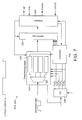
- FIG. 6 schematically shows an integrated circuit 201 in which embodiments may be incorporated.
- the integrated circuit 201 has an initiator 200 which is arranged to communicate with a target 204.
- the initiator 200 will typically issue requests which are sent to the target 204 and the target 204 will typically respond to the requests.
- the responses are typically sent back to the initiator 200.
- more than one initiator 200 may be provided and/or more than one target 204 may be provided. It should also be appreciated that a given initiator may be a target. Additionally or alternatively, a given target may also be an initiator.
- the requests output by the initiator 200 are output in a parallel format to a first serializer 206 which converts the parallel format request into a serial form.
- the serialized data is output to a first driver 208 which put the data onto a first channel 210.
- the output end of the first channel is input to a trans impedance amplifier 212.
- the output of the amplifier is input to a first deserializer 214.
- the deserializer 214 processes the received serial stream back into the parallel format.
- the requests, in the parallel format are output to the target 204.
- the responses output by the target 204 are output in a parallel format to a second serializer 216 which converts the parallel format response into a serial form.
- the serialized data is output to a driver 218 which put the data onto a second channel 220.
- the output end of the second channel is input to a driver 222.
- the output of the driver 222 is input to a second deserializer 224.
- the second deserializer 224 processes the received serial stream back into the parallel format.
- the responses, in the parallel format are output to the initiator 200.
- connection or coupling can be used for the channels 210 and 220.
- the channels may be provided by a wires, for example metal wires, optical interconnects or any other suitable connection environment or combination of two or more connection environments.
- the request and the responses to the requests may comprise data, addressing information, control signals and/or instructions. At least part of the request and response may be in packet form. In other embodiments the data can be in any other suitable format.
- a signalling protocol may be used in some embodiments. For example, in one embodiment, a node sending data may send a valid signal and a node receiving data may send an associated acknowledgement signal. It should be appreciated that no protocol may be used and/or any other signalling protocol may be used in other embodiments.
- the data is sent once the valid signal is high and the acknowledgement is confirmation of receipt of the data by the recipient.
- This valid/acknowledgement protocol may be used between the initiator and the first serializer 206/second deserializer 224 and between the target and the first deserializer 214/second serializer 216.
- FIG. 7 shows the deserializer 214 or 224 in more detail.
- the serialised data is received by a deserializing stage 226.
- the deserializing stage has a demultiplexing arrangement 227 which divides the serialized data into the constituent channels which are deserialized by the registers 229.
- the output of the deserializing stage, in parallel format is loaded by a data catcher 228.
- the registers 229 are successively output into the data catcher which acts as a data buffer.
- the output of the data catcher 228 is transferred to an interface 230 which will output the data in packet form.
- the interface 230 is also configured to implement the valid/acknowledgement protocol, generating the valid signal and receiving the acknowledgement signal.
- the interface receives a clock signal LSCLK which can be at any suitable frequency. By way of example only, the LSCLK may be at 500MHz.
- a four phase clock generator 236 is provided. The clock generator receives the output of a phase locked loop and generates four clock signals CLK1, CLK2, CLK3, and CLK4. The four clock signals have the same frequency but different phases.
- the four outputs of the clock generator 236 are input to the deserializing stage 226 and a controller 234.
- the controller receives an output from the deserializing stage 229 indicating when the data in the registers is ready for output and an output from the interface 230.
- the controller provides the four control signals to the data catcher 228 and provides a control output to the interface.
- the deserializing stage 226 also receives the output of the phase locked loop.
- the data in parallel format is received by an interface 240.
- the interface 240 is also configured to implement the valid/acknowledgement protocol, generating the acknowledgment signal in response to receiving the valid signal.
- the interface receives a clock signal LSCLK which can be at any suitable frequency.
- the LSCLK may be at 500MHz.
- the interface 240 receives a further clock signal CLK2G which can be any suitable value and in example is 2GHz.
- the data in parallel format is output by the interface 240 to a serializing stage 242.
- the serializing stage 242 has a quad parallel in serial out shift register, each register stores a quarter of the data and serializes the data.
- the registers outputs then four lower speed serial data.
- the registers 243 are each connected or coupled to a respective input of a multiplexing arrangement 245 which mixes the constituent channels into a high speed serialized data stream.
- a four phase clock generator 248 is provided.
- the clock generator receives the output of a phase locked loop and generates four clock signals CLK1, CLK2, CLK3, and CLK4.
- the four clock signals have the same frequency but decayed by 90° phase shift.
- the four clock signals have 90 degrees phase shift.
- the first clock signal has no phase shift
- the second clock signal has 180 degree phase shift
- the third clock signal has 90 degree phase shift
- the fourth has a 270 degree phase shift.
- the four outputs of the clock generator 248 are input to the serializing stage 242 and a controller 246.
- the clock generator receives an enable output from the interface 240.
- the controller provides the four clock signals to the serializing stage 242 and receives a start signal from the interface 240.
- the arrangement of Figures 1 and/or 2 may be used to generate one or more of the clock signals used in the deserializer and/or serializer of Figures 6 to 8 .
- the circuit may be modified to have only one Muller gate.
- the, second Muller gate may be omitted and the output of the first Muller gate is input to a suitable logic gate or gates such as an AND gate or OR gate or the like.
- a suitable logic gate or gates such as an AND gate or OR gate or the like.
- more than one Muller gate may be provided.
- Some embodiments may provide glitch free or glitch reduced clock. Some embodiments may be used to gate a High speed clock and/or when an enable signal domain and the clock domain are asynchronous for example in the case of a multi-clock islands system on chip.
- one or more of the delay elements may be omitted.
- the delay elements may be replaced by any other suitable delay.
- figure 9 shows the interface 240 of figure 3 .
- the interface comprises, in the example shown in figure 9 six data stores, 62, 64, 66, 68, 70 and 72.
- the first data store 62 has N inputs which comprise the parallel data which is received either from the initiator or the target.
- the first data store 62 has n outputs which allow data to be shifted to a second data store 64.
- the second, third, fourth and fifth data stores each have a respective controller 76, 78, 80 and 82.
- a first controller 74 is provided which is arranged to receive a valid (request) signal from the source of the packet. In response to that request, the first controller provides an acknowledgement signal ACK which is returned to the source of the packet.
- the valid signal is input to an automatic gating controller 88.
- the controller 74 is also arranged to provide an output to the automatic gating controller.
- the first flow controller is arranged to send the received valid signal to the second controller 76 which is arranged to provide the ACK signal to the first flow controller.
- the second controller 76 is arranged to output the valid signal to the third controller 78 which outputs the valid signal to the fourth flow controller 80 and so on until the valid signal is received by the sixth flow controller 84.
- the sixth flow controller 84 outputs the ACK signal to the fifth controller 82 which outputs the ACK signal to the fourth flow controller and so on until the ACK signal is output by the second controller 76 to the first controller 74.
- the second, third, fourth and fifth controllers are arranged to control the respective data stores. In particular, these controllers control whether or not the clock signal which is provided to the respective data store is gated or not. Thus, if there is no need for data to be received from a preceding data store or output to a succeeding data store, that is the data state is held, then no clock signal is applied to the data store, thus saving power.
- the data store can take any suitable format but may comprise an N fold flip-flop. When no clock signal is to be applied to the N fold flip-flop, a low logic level signal will be applied to the respective clock inputs of the flip-flops of the N fold flip-flop.
- the second to fifth controllers 76, 78, 80 and 82 are also configured to provide outputs to the automatic gating controller.
- a queue controller 86 is provided which has a control output which is input to each of the second to six flow controllers.
- the bank registers 62 and 62 are permanently clocked by the gated LSCLK clock.
- the automatic gating controller 88 is configured to output via a first clock gating cell 90 a first clock signal and via a second clock gating cell 92 a second clock signal.
- These gating cells may be as described in relation to Figures 1 to 5 .
- the first clock signal has a first frequency which is relatively high and may for example be 2GHz.
- the second clock signal is relatively low and may be for example 500 MHz
- the automatic gating controller is configured to generate an enable signal for enabling the clock generator 248
- the first controller 74 then outputs the valid signal to the automatic gating controller when the data is loaded in the first data store.
- the outputs of the respective clock gating cells are used to clock the arrangement of Figure 9 .
- the RS signal from the fifth controller 82 to the queue controller is the signal responsible for the reset of the counter.
- the queue controller 86 provides an output control signal CNT.
- Clock gating can be used in any products such as FPGA (field programmable gate array), DSP (digital signal processors, SoCs, microprocessors and microcontrollers.
- FPGA field programmable gate array
- DSP digital signal processors
- SoC SoCs
- microprocessors microcontrollers.
- Some embodiments may be better for both high and low frequency glitch free clock gating. Some embodiments can be used where the prior art cannot be used because of: high frequency; clock skew; signal delay; and/or asynchronism between clock islands within a multi-clock system. It should be noted that skew, delays and asynchronism may cause errors and a glitchy gated clock at low frequencies as this is related to flip flop metastability.
Landscapes
- Engineering & Computer Science (AREA)
- Theoretical Computer Science (AREA)
- Physics & Mathematics (AREA)
- General Engineering & Computer Science (AREA)
- General Physics & Mathematics (AREA)
- Semiconductor Integrated Circuits (AREA)
- Manipulation Of Pulses (AREA)
Abstract
A circuit comprises a first Muller gate having a first input configured to receive a clock signal, a second input configured to receive an enable signal and an output. A logic circuit is also provided having a first input configured to receive said clock signal, and a second input configured to receive an input dependent on said output, said logic circuit being configured to provide a gated clock output.
Description
- The present invention relates to a circuit and in particular but not exclusively to a circuit for a clock gating cell.
- Increasingly with integrated circuits, a high density of transistors is being provided leading to relatively large circuits. The interconnects, as a result, become longer and more resistive. With shrinking feature sizes, the relative resistivity of the wires is increased. Further as integrated circuit design evolves the voltages used are being reduced leading to an increase in the signal's delay. Increasingly, high speed clocks are used on integrated circuits with multi-clock islands for better system on chip (SoC) performances. A portion of the system power consumption comes from clock signals. Clock gating technique is a low power technique that reduces the switching activity of transistors and hence reduces the consumed power.
- These trends lead to problems in signal delays, skewing and signal racing which can result in metastability. In the case of a gated clock, the clock may be glitchy which can adversely affect performance.
- According to an embodiment, there is a circuit comprising: a first Muller gate having a first input configured to receive a clock signal, a second input configured to receive an enable signal and an output; and a logic circuit having a first input configured to receive said clock signal, and a second input configured to receive an input dependent on said output, said logic circuit being configured to provide a gated clock output.
- The circuit may comprise a second Muller gate.
- The second Muller gate may have a first input configured to receive the output of the first Muller gate and a second input configured to receive the clock signal.
- A first delay may be provided, said first delay being configured to delay the clock signal received by the second input of the second Muller gate.
- The second Muller gate is configured to provide an output, said output being provided to said second input of the logic circuit
- The logic circuit may be configured to provide a clock signal as said gated clock output when said enable signal is active and to provide a signal at one level when said enable signal is inactive.
- The logic circuit may comprise an AND gate.
- The logic circuit may be configured to provide a clock signal as said gated clock output when said enable signal is inactive and to provide a signal at one level when said enable signal is active.
- The logic circuit may comprise an OR gate.
- The circuit may comprises a second delay for delaying the clock signal provided to said first input of said second Muller gate.
- The clock signal may be provided to said first input of said second Muller gate.
- The second delay and the first delay may be arranged in series.
- According to another embodiment an integrated circuit comprises a circuit as discussed above.
- Reference will be made by way of example only to the following figures in which:
-
Figure 1 shows a circuit for provided a gated clock; -
Figure 2 shows a second circuit for providing a gated clock; -
Figure 3 shows the gate representation of the Muller gate used in the circuits of -
Figures 1 and 2 ; -
Figure 4 shows a CMOS implementation of a Muller gate; -
Figure 5a shows a first timing diagram for the circuits ofFigure 1 and Figure 2 in the in an ideal case when there is no clock skew and no enable signal delay; -
Figure 5b shows a second timing diagram for the circuits ofFigure 1 and Figure 2 in the case when there is a positive clock skew and/or negative enable signal delay; -
Figure 5c shows a third timing diagram for the circuits ofFigure 1 and Figure 2 in the in the case when there is a negative clock skew and/or positive enable signal delay; -
Figure 6 schematically shows an integrated circuit; -
Figure 7 shows the deserializer ofFigure 6 in more detail; -
Figure 8 shows the serializer ofFigure 6 in more detail; -
Figure 9 shows schematically the interface of the serializer offigure 3 ; - It has been proposed to provide glitch free clock gating where a clock signal and an enable signal are provided as inputs to an AND gate. The output provides a gated clock. However glitches may occur due to the early or late arrival time of the enable signal in some scenarios. In particular, glitches may occur as a result of signal race and may happen when the skew is relatively high and/or when the enable signal comes from another clock domain. The skew can be positive or negative.
- It has also been proposed to provide latch based clock gating. An enable signal is provided into the D input of a latch with a clock signal being provided as a clock input and the Q output being provided to an input of the logic gate along with the clock signal being provided to a second input of the logic gate. The output of the logic gate provides the gated clock signal. However such an arrangement is not efficient when the frequency of the enable domain and the clock frequency are asynchronous. Metastability of the latches may occur due to skew, delay or high clock frequency utilization.
- Reference is now made to
Figure 1 which shows an asynchronous logic based circuit which is arranged to provide a gated clock output. In other words the clock which is supplied to a circuit can be disabled or switched off to save power. Embodiments may use a C_element, also known as a Muller gate. InFigure 1 , a first Mullergate 2 is provided with aclock input 4 and an enableinput 6. It should be noted that the clock signal is inverted prior to being input to the first Mullergate 2 The clock signal is inverted to prevent a glitch during the first clock cycle in of the gated clock in the case where there is a negative clock skew and/or a positive delay of the Enable signal (as will be explained in more detail with reference toFigure 5c ). Theoutput 8 of the first Mullergate 2 is input to a second Mullergate 10. The second Mullergate 10 also receives an input from theclock source 4. However, the clock signal is input to afirst delay element 12 prior to being input to the second Mullergate 10. The role of thedelay element 12 is to retard the clock signal by a delay equal to the propagation delay of the Mullergate 2. Theoutput 14 of the second Muller gate is input to a first ANDgate 16. The output of thefirst delay element 12 is also input to asecond delay element 18, the output of which provides a second input to thefirst AND gate 16. The role of thedelay element 18 is to retard the output of thefirst delay element 12 by a delay equal to the propagation delay of the Mullergate 10.Delay elements gates - The output of the
AND gate 16 provides a first gated clock signal. - The delays may be provided to avoid signal racing. The arrangements can be used to avoid glitches.
- Reference is made to
Figure 2 which shows a similar arrangement to that shown inFigure 1 , with those same elements marked with the same reference number. However, theAND gate 16 has been replaced by anOR gate 18 which provides a second gated clock signal. - Some embodiments have a relatively low transistor count, for example of the order of 30 transistors. The circuits may be efficient even if the frequency of the enable domain and the clock domain are asynchronous.
- Reference is made to
Figure 3 which shows schematically the gate representation of the Muller gate. TheMuller gate 20 has an ainput 22,a b input 24 and ans output 26. The truth table for the Muller gate is represented below.a b S 0 0 0 0 1 s- 1 0 s- 1 1 1 - It should be appreciated that the s- notation means that the output is unchanged.
- The output can be represented mathematically as follows: s = ab + s (a + b)
- The Muller gate is a gate used for the design of asynchronous systems. The Muller gate is used to ensure the synchronization or rendezvous between asynchronous signals.
- Reference is now made to
Figure 4 which schematically shows the Van Berkel transistor-level implementation of the Muller gate which uses MOS transistors. Between a voltage supply VDD and ground are arranged in series from VDD go ground in the following order: a first P type transistor P1; a second P type transistor P2; a second N type transistor N2; and a second N type transistor N1. The gates of the first P type transistor P1 and the first N type transistor N1 are connected or coupled to the A input whilst the gate inputs of the second P and N transistors P2 and N2 are connected or coupled to the B input. - Arranged in parallel to this first series of transistors is a second set of transistors, again connected or coupled between VDD and ground in series in the following order: a fourth P type transistor P4, a fifth P type transistor P5, a fifth N type transistor N5 and a fourth N type transistor N4. The gate element of the fourth P type transistor P4 and the date of the fourth N type transistor N4 are connected or coupled to the B input. The gate inputs of the fifth N and P type transistors N5 and P5 are connected or coupled to the A input.
- In parallel with the first and in parallel with the second set of series transistors is a third set of series transistors arranged between VDD and ground. Again, the transistors are connected or coupled in the following order from VDD to ground: A sixth P type transistor P6 and a sixth N type transistor N6. The gates of the sixth N type and P type transistors N6 and P6 are coupled together and are coupled to a node between the fifth and sixth P type and N type transistors N5 and P5 as well as to a node between the second N and P type transistors N2 and P2 and provide the S' output. The S output is provided by a node which is provided between the sixth N and P type transistors N6 and P6.
- A third P type transistor is arranged between a node between the first and second P type transistors and a further node between the fourth and fifth P type transistors. The control gate of the third P type transistor is connected or coupled to the S output provided by the node between the fixed N and P type transistors N6 and P6. Likewise, a third N type transistor N3 is provided between a first node located between the first and second N type transistors N1 and N2 and a second node provided between the fourth and fifth N type transistors N4 and N5. Again, the gate element of the third N type transistor is connected or coupled to the S output node.
- It should be appreciated that
Figure 4 shows one way of implementing the gate. Alternative implementation may be used to provide the Muller gate. - Reference is made to
Figures 5a which shows a first timing diagram for the circuits ofFigure 1 and Figure 2 . The first line of the timing diagram shows theclock signal 4. The second line shows the enablesignal 6. The third line shows theoutput 8 of thefirst Muller gate 2 whilst the fourth line shows theoutput 14 of thesecond Muller gate 10. The fifth line shows the gatedclock output signal 19 of the ANDgate 16 whilst the final line shows thegated clock signal 21 output by theOR gate 18. - In the arrangement shown on
Figure 5a , the enablesignal 6 changes, low state to a high state (the enable state) at the same time that the clock transitions, low state to a high state. The output of the first Muller gate transitions to the high state at the next clock edge which an example ofFigure 5a is the next falling clock edge. The output of the second Muller gate goes high after the output of the first Muller gate has gone high, at the next clock edge, which is a rising clock edge. With the arrangement ofFigure 1 , the clock signal output by the AND gate is low until the output of thesecond Muller gate 10 goes high. Once the output of the first Muller gate goes high, the clock signal output by the ANDgate 16 follows theclock signal 4. - In contrast, in the arrangement shown in
Figure 2 , the clock signal output by theOR gate 18 follows the input clock signal until the output of the second Muller gate goes high. At that point, the gated clock signal output by the OR gate simply stays at the high level. - When the enable signal goes low, this causes the
output 8 of the first Muller gate to go low. This in turn causes the output of the second Muller gate also to go low, at the next clock edge which in the example shown inFigure 5a is a falling clock edge. This will cause thegated clock signal 19 output by the first ANDgate 16 to be low. In contrast, theclock signal 21 output via theOR gate 18 starts to follow theclock signal 4. -
Figure 5b is similar to that shown inFigure 5a . However, the enable signal changes midway during a low point in theclock cycle 4. The output of the first Muller gate immediately follows the enable signal and goes high. Theoutput 14 of the second Muller gate goes high at the next change in the clock signal which is a rising edge. - When the enable signal goes low, it is partway through the low part of the clock signal. The output of the first Muller gate goes to the low value at the next change in the clock signal which is a rising edge of the clock signal. The output of the second Muller gate then goes to the low value at the next change in the clock signal which is a falling edge of the clock signal in this case.
- The first and second clock signals follow the same pattern of the
output signal 14 of the second Muller gate as described in relation toFigure 5a . Reference is now made toFigure 5c which shows the enable signal rising midway through a period when the clock signal is high. The signals are as shown inFigures 5a and 5b . The output of the first Muller gate follows the enable signal and goes high at the next clock edge, which is a falling clock edge in this case. Theoutput 14 of the second Muller gate goes high at the next change in the clock signal which is a rising edge in this case. - When the enable signal goes low, it is partway through the high part of the clock signal. The output of the first Muller gate goes to the low value more or less at the same time. The output of the second Muller gate then goes to the low value state at the next change in the clock signal which is a falling edge of the clock signal in this case. In this case, the output goes to the low state while the ouput 21 starts to follow the
clock signal 4, - In the embodiments shown, AND or OR gates are used. It should be appreciated that in alternative embodiments, different logic gates or gates can be used.
- Reference is made to
Figure 6 which schematically shows anintegrated circuit 201 in which embodiments may be incorporated. Theintegrated circuit 201 has aninitiator 200 which is arranged to communicate with atarget 204. Theinitiator 200 will typically issue requests which are sent to thetarget 204 and thetarget 204 will typically respond to the requests. The responses are typically sent back to theinitiator 200. - It should be appreciated that in practice, more than one
initiator 200 may be provided and/or more than onetarget 204 may be provided. It should also be appreciated that a given initiator may be a target. Additionally or alternatively, a given target may also be an initiator. - The requests output by the
initiator 200 are output in a parallel format to afirst serializer 206 which converts the parallel format request into a serial form. The serialized data is output to afirst driver 208 which put the data onto afirst channel 210. The output end of the first channel is input to atrans impedance amplifier 212. The output of the amplifier is input to afirst deserializer 214. Thedeserializer 214 processes the received serial stream back into the parallel format. The requests, in the parallel format, are output to thetarget 204. - A similar path is provided for the responses to the request. The responses output by the
target 204 are output in a parallel format to asecond serializer 216 which converts the parallel format response into a serial form. The serialized data is output to adriver 218 which put the data onto asecond channel 220. The output end of the second channel is input to adriver 222. The output of thedriver 222 is input to asecond deserializer 224. Thesecond deserializer 224 processes the received serial stream back into the parallel format. The responses, in the parallel format, are output to theinitiator 200. - It should be appreciated that any suitable connection or coupling can be used for the
channels - The request and the responses to the requests may comprise data, addressing information, control signals and/or instructions. At least part of the request and response may be in packet form. In other embodiments the data can be in any other suitable format. A signalling protocol may be used in some embodiments. For example, in one embodiment, a node sending data may send a valid signal and a node receiving data may send an associated acknowledgement signal. It should be appreciated that no protocol may be used and/or any other signalling protocol may be used in other embodiments.
- In some embodiments the data is sent once the valid signal is high and the acknowledgement is confirmation of receipt of the data by the recipient. This valid/acknowledgement protocol may be used between the initiator and the
first serializer 206/second deserializer 224 and between the target and thefirst deserializer 214/second serializer 216. - Reference is made to
Figure7 which shows thedeserializer deserializing stage 226. The deserializing stage has ademultiplexing arrangement 227 which divides the serialized data into the constituent channels which are deserialized by theregisters 229. The output of the deserializing stage, in parallel format is loaded by adata catcher 228. Theregisters 229 are successively output into the data catcher which acts as a data buffer. - The output of the
data catcher 228 is transferred to aninterface 230 which will output the data in packet form. Theinterface 230 is also configured to implement the valid/acknowledgement protocol, generating the valid signal and receiving the acknowledgement signal. The interface receives a clock signal LSCLK which can be at any suitable frequency. By way of example only, the LSCLK may be at 500MHz. A fourphase clock generator 236 is provided. The clock generator receives the output of a phase locked loop and generates four clock signals CLK1, CLK2, CLK3, and CLK4. The four clock signals have the same frequency but different phases. The four outputs of theclock generator 236 are input to thedeserializing stage 226 and acontroller 234. The controller receives an output from thedeserializing stage 229 indicating when the data in the registers is ready for output and an output from theinterface 230. - The controller provides the four control signals to the
data catcher 228 and provides a control output to the interface. Thedeserializing stage 226 also receives the output of the phase locked loop. - Reference is made to
Figure 8 which shows theserializer interface 240. Theinterface 240 is also configured to implement the valid/acknowledgement protocol, generating the acknowledgment signal in response to receiving the valid signal. The interface receives a clock signal LSCLK which can be at any suitable frequency. By way of example only, the LSCLK may be at 500MHz. Theinterface 240 receives a further clock signal CLK2G which can be any suitable value and in example is 2GHz. - The data in parallel format is output by the
interface 240 to a serializingstage 242. The serializingstage 242 has a quad parallel in serial out shift register, each register stores a quarter of the data and serializes the data. The registers outputs then four lower speed serial data. Theregisters 243 are each connected or coupled to a respective input of amultiplexing arrangement 245 which mixes the constituent channels into a high speed serialized data stream. - A four
phase clock generator 248 is provided. The clock generator receives the output of a phase locked loop and generates four clock signals CLK1, CLK2, CLK3, and CLK4. The four clock signals have the same frequency but decayed by 90° phase shift. - In particular, the four clock signals have 90 degrees phase shift. Thus the first clock signal has no phase shift, the second clock signal has 180 degree phase shift, the third clock signal has 90 degree phase shift and the fourth has a 270 degree phase shift.The four outputs of the
clock generator 248 are input to the serializingstage 242 and acontroller 246. The clock generator receives an enable output from theinterface 240. The controller provides the four clock signals to the serializingstage 242 and receives a start signal from theinterface 240. - In some embodiments the arrangement of
Figures 1 and/or 2 may be used to generate one or more of the clock signals used in the deserializer and/or serializer ofFigures 6 to 8 . - In some embodiments, the circuit may be modified to have only one Muller gate. For example the, second Muller gate may be omitted and the output of the first Muller gate is input to a suitable logic gate or gates such as an AND gate or OR gate or the like. In alternative embodiments more than one Muller gate may be provided.
- Some embodiments may provide glitch free or glitch reduced clock. Some embodiments may be used to gate a High speed clock and/or when an enable signal domain and the clock domain are asynchronous for example in the case of a multi-clock islands system on chip.
- In some embodiments, one or more of the delay elements may be omitted. The delay elements may be replaced by any other suitable delay.
- Reference is made to
figure 9 which shows theinterface 240 offigure 3 . - The interface comprises, in the example shown in
figure 9 six data stores, 62, 64, 66, 68, 70 and 72. Thefirst data store 62 has N inputs which comprise the parallel data which is received either from the initiator or the target. Thefirst data store 62 has n outputs which allow data to be shifted to asecond data store 64. - Likewise, the output of the
second data store 64 can be shifted to thethird data store 66 and so on. The second, third, fourth and fifth data stores each have arespective controller first controller 74 is provided which is arranged to receive a valid (request) signal from the source of the packet. In response to that request, the first controller provides an acknowledgement signal ACK which is returned to the source of the packet. The valid signal is input to anautomatic gating controller 88. Thecontroller 74 is also arranged to provide an output to the automatic gating controller. The first flow controller is arranged to send the received valid signal to thesecond controller 76 which is arranged to provide the ACK signal to the first flow controller. Likewise, thesecond controller 76 is arranged to output the valid signal to thethird controller 78 which outputs the valid signal to thefourth flow controller 80 and so on until the valid signal is received by thesixth flow controller 84. Thesixth flow controller 84 outputs the ACK signal to thefifth controller 82 which outputs the ACK signal to the fourth flow controller and so on until the ACK signal is output by thesecond controller 76 to thefirst controller 74. The second, third, fourth and fifth controllers are arranged to control the respective data stores. In particular, these controllers control whether or not the clock signal which is provided to the respective data store is gated or not. Thus, if there is no need for data to be received from a preceding data store or output to a succeeding data store, that is the data state is held, then no clock signal is applied to the data store, thus saving power. - The data store can take any suitable format but may comprise an N fold flip-flop. When no clock signal is to be applied to the N fold flip-flop, a low logic level signal will be applied to the respective clock inputs of the flip-flops of the N fold flip-flop. The second to
fifth controllers queue controller 86 is provided which has a control output which is input to each of the second to six flow controllers. The bank registers 62 and 62 are permanently clocked by the gated LSCLK clock. - When the valid signal is logic high, the
automatic gating controller 88 is configured to output via a first clock gating cell 90 a first clock signal and via a second clock gating cell 92 a second clock signal. These gating cells may be as described in relation toFigures 1 to 5 .The first clock signal has a first frequency which is relatively high and may for example be 2GHz. The second clock signal is relatively low and may be for example 500 MHz Further, the automatic gating controller is configured to generate an enable signal for enabling theclock generator 248 Thefirst controller 74 then outputs the valid signal to the automatic gating controller when the data is loaded in the first data store. The outputs of the respective clock gating cells are used to clock the arrangement ofFigure 9 . - The RS signal from the
fifth controller 82 to the queue controller is the signal responsible for the reset of the counter. Thequeue controller 86 provides an output control signal CNT. - Clock gating can be used in any products such as FPGA (field programmable gate array), DSP (digital signal processors, SoCs, microprocessors and microcontrollers.
- Some embodiments may be better for both high and low frequency glitch free clock gating. Some embodiments can be used where the prior art cannot be used because of: high frequency; clock skew; signal delay; and/or asynchronism between clock islands within a multi-clock system. It should be noted that skew, delays and asynchronism may cause errors and a glitchy gated clock at low frequencies as this is related to flip flop metastability.
- The foregoing description has provided by way of exemplary and non-limiting examples a full and informative description of the exemplary embodiment of this invention. However, various modifications and adaptations may become apparent to those skilled in the relevant arts in view of the foregoing description, when read in conjunction with the accompanying drawings and the appended claims. However, all such and similar modifications of the teachings of this invention will still fall within the scope of this invention as defined in the appended claims.
Claims (13)
- A circuit comprising:a first Muller gate having a first input configured to receive a clock signal, a second input configured to receive an enable signal and an output; anda logic circuit having a first input configured to receive said clock signal, and a second input configured to receive an input dependent on said output, said logic circuit being configured to provide a gated clock output.
- A circuit as claimed in claim 1, comprising a second Muller gate.
- A circuit as claimed in claim 2, wherein said second Muller gate has a first input configured to receive the output of the first Muller gate and a second input configured to receive the clock signal.
- A circuit as claimed in claim 3, wherein a first delay is provided, said first delay being configured to delay the clock signal received by the second input of the second Muller gate.
- A circuit as claimed in any of claims 2 to 4, wherein said second Muller gate is configured to provide an output, said output being provided to said second input of the logic circuit
- A circuit as claimed in any preceding claim, wherein said logic circuit is configured to provide a clock signal as said gated clock output when said enable signal is active and to provide a signal at one level when said enable signal is inactive.
- A circuit as claimed in claim 6, wherein said logic circuit comprises an AND gate.
- A circuit as claimed in any of claims 1 to 5, wherein said logic circuit is configured to provide a clock signal as said gated clock output when said enable signal is inactive and to provide a signal at one level when said enable signal is active.
- A circuit as claimed in claim 8, wherein said logic circuit comprises an OR gate.
- A circuit as claimed in any preceding claim, comprising a second delay for delaying the clock signal provided to said first input of said second Muller gate.
- A circuit as claimed in claim 3 or any claim appended thereto wherein said clock signal provided to said first input of said second Muller gate has passed through said first delay.
- A circuit as claimed in claim 11 when appended to claim 10, wherein said second delay and said first delay are arranged in series.
- An integrated circuit comprising a circuit as claimed in any preceding claim.
Priority Applications (2)
| Application Number | Priority Date | Filing Date | Title |
|---|---|---|---|
| EP11425114A EP2515197A1 (en) | 2011-04-21 | 2011-04-21 | Clock gating circuit using a Muller C- element |
| US13/450,618 US8570069B2 (en) | 2011-04-21 | 2012-04-19 | Clock gating cell circuit |
Applications Claiming Priority (1)
| Application Number | Priority Date | Filing Date | Title |
|---|---|---|---|
| EP11425114A EP2515197A1 (en) | 2011-04-21 | 2011-04-21 | Clock gating circuit using a Muller C- element |
Publications (1)
| Publication Number | Publication Date |
|---|---|
| EP2515197A1 true EP2515197A1 (en) | 2012-10-24 |
Family
ID=44719806
Family Applications (1)
| Application Number | Title | Priority Date | Filing Date |
|---|---|---|---|
| EP11425114A Withdrawn EP2515197A1 (en) | 2011-04-21 | 2011-04-21 | Clock gating circuit using a Muller C- element |
Country Status (2)
| Country | Link |
|---|---|
| US (1) | US8570069B2 (en) |
| EP (1) | EP2515197A1 (en) |
Cited By (3)
| Publication number | Priority date | Publication date | Assignee | Title |
|---|---|---|---|---|
| CN105591728A (en) * | 2014-11-10 | 2016-05-18 | 英特尔公司 | Link Layer Signal Synchronization |
| RU2592466C1 (en) * | 2015-06-11 | 2016-07-20 | Федеральное государственное учреждение "Федеральный научный центр Научно-исследовательский институт системных исследований Российской академии наук" (ФГУ ФНЦ НИИСИ РАН) | Synchro-stratum module, coordinating concurrent operation of controlled unit in globally asynchronous system |
| RU2592462C1 (en) * | 2015-04-07 | 2016-07-20 | Федеральное государственное учреждение "Федеральный научный центр Научно-исследовательский институт системных исследований Российской академии наук"(ФГУ ФНЦ НИИСИ РАН) | Synchrostratum module for wave processing of data |
Families Citing this family (6)
| Publication number | Priority date | Publication date | Assignee | Title |
|---|---|---|---|---|
| KR102204597B1 (en) * | 2014-11-19 | 2021-01-19 | 삼성전자주식회사 | Semiconductor device |
| KR102261300B1 (en) | 2015-06-22 | 2021-06-09 | 삼성전자주식회사 | Clock gating circuit operating at high speed |
| US9360883B1 (en) | 2015-08-26 | 2016-06-07 | Freescale Semiconductor, Inc. | Clock multiplexer for generating glitch-free clock signal |
| US9490789B1 (en) * | 2016-04-27 | 2016-11-08 | Freescale Semiconductor, Inc. | Glitch-free clock switching circuit using Muller C-elements |
| US11543849B2 (en) | 2019-04-22 | 2023-01-03 | Samsung Electronics Co., Ltd. | Integrated clock gater latch structures with adjustable output reset |
| US10848137B1 (en) * | 2019-05-08 | 2020-11-24 | Ati Technologies Ulc | Symmetrical balanced c-element |
Citations (1)
| Publication number | Priority date | Publication date | Assignee | Title |
|---|---|---|---|---|
| US5646554A (en) * | 1995-03-16 | 1997-07-08 | Research Foundation Of State University Of New York | Method and apparatus for selective clocking using a Muller-C element |
Family Cites Families (5)
| Publication number | Priority date | Publication date | Assignee | Title |
|---|---|---|---|---|
| US7131092B2 (en) * | 2004-12-21 | 2006-10-31 | Via Technologies, Inc. | Clock gating circuit |
| JP2007184847A (en) * | 2006-01-10 | 2007-07-19 | Nec Electronics Corp | Clock and data recovery circuit and serdes circuit |
| US20100097131A1 (en) * | 2007-09-03 | 2010-04-22 | John Bainbridge | Hardening of self-timed circuits against glitches |
| US7844843B2 (en) * | 2008-12-22 | 2010-11-30 | International Business Machines Corporation | Implementing power savings in HSS clock-gating circuit |
| US8390328B2 (en) * | 2011-05-13 | 2013-03-05 | Arm Limited | Supplying a clock signal and a gated clock signal to synchronous elements |
-
2011
- 2011-04-21 EP EP11425114A patent/EP2515197A1/en not_active Withdrawn
-
2012
- 2012-04-19 US US13/450,618 patent/US8570069B2/en not_active Expired - Fee Related
Patent Citations (1)
| Publication number | Priority date | Publication date | Assignee | Title |
|---|---|---|---|---|
| US5646554A (en) * | 1995-03-16 | 1997-07-08 | Research Foundation Of State University Of New York | Method and apparatus for selective clocking using a Muller-C element |
Cited By (3)
| Publication number | Priority date | Publication date | Assignee | Title |
|---|---|---|---|---|
| CN105591728A (en) * | 2014-11-10 | 2016-05-18 | 英特尔公司 | Link Layer Signal Synchronization |
| RU2592462C1 (en) * | 2015-04-07 | 2016-07-20 | Федеральное государственное учреждение "Федеральный научный центр Научно-исследовательский институт системных исследований Российской академии наук"(ФГУ ФНЦ НИИСИ РАН) | Synchrostratum module for wave processing of data |
| RU2592466C1 (en) * | 2015-06-11 | 2016-07-20 | Федеральное государственное учреждение "Федеральный научный центр Научно-исследовательский институт системных исследований Российской академии наук" (ФГУ ФНЦ НИИСИ РАН) | Synchro-stratum module, coordinating concurrent operation of controlled unit in globally asynchronous system |
Also Published As
| Publication number | Publication date |
|---|---|
| US20120268168A1 (en) | 2012-10-25 |
| US8570069B2 (en) | 2013-10-29 |
Similar Documents
| Publication | Publication Date | Title |
|---|---|---|
| EP2515197A1 (en) | Clock gating circuit using a Muller C- element | |
| US8484523B2 (en) | Sequential digital circuitry with test scan | |
| US8122279B2 (en) | Multiphase clocking systems with ring bus architecture | |
| US8659336B2 (en) | Apparatus and method for synchronising signals | |
| KR101441028B1 (en) | Low power serdes architecture using serial i/o burst gating | |
| US7583106B2 (en) | Clock circuitry | |
| US8644439B2 (en) | Circuits and methods for signal transfer between different clock domains | |
| US10084434B2 (en) | Relative timed clock gating cell | |
| US8977882B2 (en) | System for data transfer between asynchronous clock domains | |
| US8930742B2 (en) | Clock signals for dynamic reconfiguration of communication link bundles | |
| US8975921B1 (en) | Synchronous clock multiplexer | |
| US20030210603A1 (en) | Method and apparatus for performing signal synchronization | |
| US20230367361A1 (en) | Asynchronous asic | |
| US8948215B2 (en) | High speed and high jitter tolerance dispatcher | |
| US6640277B1 (en) | Input staging logic for latching source synchronous data | |
| US6999542B1 (en) | Data ready indicator between different clock domains | |
| US9729153B1 (en) | Multimode multiplexer-based circuit | |
| US8707080B1 (en) | Simple circular asynchronous clock domain crossing technique for digital data | |
| WO2009136875A1 (en) | Synchronous sequential logic device using double triggered flip-flops and method for skewed triggering such state storing registers | |
| US7290159B2 (en) | Fixed latency data computation and chip crossing circuits and methods for synchronous input to output protocol translator supporting multiple reference oscillator frequencies | |
| EP3739463B1 (en) | Circuit for asynchronous data transfer | |
| EP2515443A1 (en) | Data serializer | |
| CN113168205B (en) | Apparatus for transaction-based transmit clock gating for low power designs | |
| JP3667461B2 (en) | Pulse generation circuit and semiconductor integrated circuit device having the same | |
| JP2000353939A (en) | Clock signal synchronous flip flop circuit |
Legal Events
| Date | Code | Title | Description |
|---|---|---|---|
| PUAI | Public reference made under article 153(3) epc to a published international application that has entered the european phase |
Free format text: ORIGINAL CODE: 0009012 |
|
| AK | Designated contracting states |
Kind code of ref document: A1 Designated state(s): AL AT BE BG CH CY CZ DE DK EE ES FI FR GB GR HR HU IE IS IT LI LT LU LV MC MK MT NL NO PL PT RO RS SE SI SK SM TR |
|
| AX | Request for extension of the european patent |
Extension state: BA ME |
|
| STAA | Information on the status of an ep patent application or granted ep patent |
Free format text: STATUS: THE APPLICATION IS DEEMED TO BE WITHDRAWN |
|
| 18D | Application deemed to be withdrawn |
Effective date: 20130425 |