EP2381571A2 - Charging systems with direct charging port support and extended capabilities - Google Patents
Charging systems with direct charging port support and extended capabilities Download PDFInfo
- Publication number
- EP2381571A2 EP2381571A2 EP11162198A EP11162198A EP2381571A2 EP 2381571 A2 EP2381571 A2 EP 2381571A2 EP 11162198 A EP11162198 A EP 11162198A EP 11162198 A EP11162198 A EP 11162198A EP 2381571 A2 EP2381571 A2 EP 2381571A2
- Authority
- EP
- European Patent Office
- Prior art keywords
- power converter
- power
- electronic device
- data
- data line
- Prior art date
- Legal status (The legal status is an assumption and is not a legal conclusion. Google has not performed a legal analysis and makes no representation as to the accuracy of the status listed.)
- Granted
Links
- 239000000523 sample Substances 0.000 claims abstract description 14
- 238000000034 method Methods 0.000 claims description 14
- 230000006854 communication Effects 0.000 abstract description 20
- 230000006870 function Effects 0.000 abstract description 10
- 230000011664 signaling Effects 0.000 description 7
- 230000006399 behavior Effects 0.000 description 4
- 239000003990 capacitor Substances 0.000 description 4
- 238000010586 diagram Methods 0.000 description 4
- 238000007726 management method Methods 0.000 description 4
- 238000012546 transfer Methods 0.000 description 4
- 101000596041 Homo sapiens Plastin-1 Proteins 0.000 description 3
- 102100035181 Plastin-1 Human genes 0.000 description 3
- 238000013459 approach Methods 0.000 description 3
- 230000007175 bidirectional communication Effects 0.000 description 3
- 230000001413 cellular effect Effects 0.000 description 3
- 230000002093 peripheral effect Effects 0.000 description 3
- 230000008569 process Effects 0.000 description 3
- 101000596046 Homo sapiens Plastin-2 Proteins 0.000 description 2
- 102100035182 Plastin-2 Human genes 0.000 description 2
- 230000002457 bidirectional effect Effects 0.000 description 2
- 238000001514 detection method Methods 0.000 description 2
- 238000005259 measurement Methods 0.000 description 2
- HBBGRARXTFLTSG-UHFFFAOYSA-N Lithium ion Chemical compound [Li+] HBBGRARXTFLTSG-UHFFFAOYSA-N 0.000 description 1
- 230000002411 adverse Effects 0.000 description 1
- 230000005540 biological transmission Effects 0.000 description 1
- 230000008859 change Effects 0.000 description 1
- 230000001747 exhibiting effect Effects 0.000 description 1
- 230000036541 health Effects 0.000 description 1
- 229910001416 lithium ion Inorganic materials 0.000 description 1
- 230000013011 mating Effects 0.000 description 1
- 238000012986 modification Methods 0.000 description 1
- 230000004048 modification Effects 0.000 description 1
- 230000010363 phase shift Effects 0.000 description 1
- 238000012384 transportation and delivery Methods 0.000 description 1
- 238000013024 troubleshooting Methods 0.000 description 1
Images


Classifications
-
- H—ELECTRICITY
- H02—GENERATION; CONVERSION OR DISTRIBUTION OF ELECTRIC POWER
- H02M—APPARATUS FOR CONVERSION BETWEEN AC AND AC, BETWEEN AC AND DC, OR BETWEEN DC AND DC, AND FOR USE WITH MAINS OR SIMILAR POWER SUPPLY SYSTEMS; CONVERSION OF DC OR AC INPUT POWER INTO SURGE OUTPUT POWER; CONTROL OR REGULATION THEREOF
- H02M1/00—Details of apparatus for conversion
- H02M1/10—Arrangements incorporating converting means for enabling loads to be operated at will from different kinds of power supplies, e.g. from ac or dc
-
- H—ELECTRICITY
- H02—GENERATION; CONVERSION OR DISTRIBUTION OF ELECTRIC POWER
- H02J—CIRCUIT ARRANGEMENTS OR SYSTEMS FOR SUPPLYING OR DISTRIBUTING ELECTRIC POWER; SYSTEMS FOR STORING ELECTRIC ENERGY
- H02J7/00—Circuit arrangements for charging or depolarising batteries or for supplying loads from batteries
- H02J7/007—Regulation of charging or discharging current or voltage
-
- G—PHYSICS
- G01—MEASURING; TESTING
- G01L—MEASURING FORCE, STRESS, TORQUE, WORK, MECHANICAL POWER, MECHANICAL EFFICIENCY, OR FLUID PRESSURE
- G01L1/00—Measuring force or stress, in general
- G01L1/20—Measuring force or stress, in general by measuring variations in ohmic resistance of solid materials or of electrically-conductive fluids; by making use of electrokinetic cells, i.e. liquid-containing cells wherein an electrical potential is produced or varied upon the application of stress
- G01L1/205—Measuring force or stress, in general by measuring variations in ohmic resistance of solid materials or of electrically-conductive fluids; by making use of electrokinetic cells, i.e. liquid-containing cells wherein an electrical potential is produced or varied upon the application of stress using distributed sensing elements
-
- G—PHYSICS
- G01—MEASURING; TESTING
- G01R—MEASURING ELECTRIC VARIABLES; MEASURING MAGNETIC VARIABLES
- G01R27/00—Arrangements for measuring resistance, reactance, impedance, or electric characteristics derived therefrom
- G01R27/02—Measuring real or complex resistance, reactance, impedance, or other two-pole characteristics derived therefrom, e.g. time constant
-
- G—PHYSICS
- G06—COMPUTING; CALCULATING OR COUNTING
- G06F—ELECTRIC DIGITAL DATA PROCESSING
- G06F1/00—Details not covered by groups G06F3/00 - G06F13/00 and G06F21/00
- G06F1/26—Power supply means, e.g. regulation thereof
- G06F1/266—Arrangements to supply power to external peripherals either directly from the computer or under computer control, e.g. supply of power through the communication port, computer controlled power-strips
-
- H—ELECTRICITY
- H02—GENERATION; CONVERSION OR DISTRIBUTION OF ELECTRIC POWER
- H02J—CIRCUIT ARRANGEMENTS OR SYSTEMS FOR SUPPLYING OR DISTRIBUTING ELECTRIC POWER; SYSTEMS FOR STORING ELECTRIC ENERGY
- H02J7/00—Circuit arrangements for charging or depolarising batteries or for supplying loads from batteries
- H02J7/00032—Circuit arrangements for charging or depolarising batteries or for supplying loads from batteries characterised by data exchange
- H02J7/00036—Charger exchanging data with battery
-
- H—ELECTRICITY
- H02—GENERATION; CONVERSION OR DISTRIBUTION OF ELECTRIC POWER
- H02J—CIRCUIT ARRANGEMENTS OR SYSTEMS FOR SUPPLYING OR DISTRIBUTING ELECTRIC POWER; SYSTEMS FOR STORING ELECTRIC ENERGY
- H02J7/00—Circuit arrangements for charging or depolarising batteries or for supplying loads from batteries
- H02J7/02—Circuit arrangements for charging or depolarising batteries or for supplying loads from batteries for charging batteries from ac mains by converters
- H02J7/04—Regulation of charging current or voltage
-
- H—ELECTRICITY
- H02—GENERATION; CONVERSION OR DISTRIBUTION OF ELECTRIC POWER
- H02M—APPARATUS FOR CONVERSION BETWEEN AC AND AC, BETWEEN AC AND DC, OR BETWEEN DC AND DC, AND FOR USE WITH MAINS OR SIMILAR POWER SUPPLY SYSTEMS; CONVERSION OF DC OR AC INPUT POWER INTO SURGE OUTPUT POWER; CONTROL OR REGULATION THEREOF
- H02M3/00—Conversion of dc power input into dc power output
- H02M3/02—Conversion of dc power input into dc power output without intermediate conversion into ac
- H02M3/04—Conversion of dc power input into dc power output without intermediate conversion into ac by static converters
- H02M3/06—Conversion of dc power input into dc power output without intermediate conversion into ac by static converters using resistors or capacitors, e.g. potential divider
- H02M3/07—Conversion of dc power input into dc power output without intermediate conversion into ac by static converters using resistors or capacitors, e.g. potential divider using capacitors charged and discharged alternately by semiconductor devices with control electrode, e.g. charge pumps
-
- H—ELECTRICITY
- H02—GENERATION; CONVERSION OR DISTRIBUTION OF ELECTRIC POWER
- H02M—APPARATUS FOR CONVERSION BETWEEN AC AND AC, BETWEEN AC AND DC, OR BETWEEN DC AND DC, AND FOR USE WITH MAINS OR SIMILAR POWER SUPPLY SYSTEMS; CONVERSION OF DC OR AC INPUT POWER INTO SURGE OUTPUT POWER; CONTROL OR REGULATION THEREOF
- H02M3/00—Conversion of dc power input into dc power output
- H02M3/02—Conversion of dc power input into dc power output without intermediate conversion into ac
- H02M3/04—Conversion of dc power input into dc power output without intermediate conversion into ac by static converters
- H02M3/10—Conversion of dc power input into dc power output without intermediate conversion into ac by static converters using discharge tubes with control electrode or semiconductor devices with control electrode
- H02M3/145—Conversion of dc power input into dc power output without intermediate conversion into ac by static converters using discharge tubes with control electrode or semiconductor devices with control electrode using devices of a triode or transistor type requiring continuous application of a control signal
- H02M3/155—Conversion of dc power input into dc power output without intermediate conversion into ac by static converters using discharge tubes with control electrode or semiconductor devices with control electrode using devices of a triode or transistor type requiring continuous application of a control signal using semiconductor devices only
- H02M3/156—Conversion of dc power input into dc power output without intermediate conversion into ac by static converters using discharge tubes with control electrode or semiconductor devices with control electrode using devices of a triode or transistor type requiring continuous application of a control signal using semiconductor devices only with automatic control of output voltage or current, e.g. switching regulators
- H02M3/158—Conversion of dc power input into dc power output without intermediate conversion into ac by static converters using discharge tubes with control electrode or semiconductor devices with control electrode using devices of a triode or transistor type requiring continuous application of a control signal using semiconductor devices only with automatic control of output voltage or current, e.g. switching regulators including plural semiconductor devices as final control devices for a single load
-
- H—ELECTRICITY
- H02—GENERATION; CONVERSION OR DISTRIBUTION OF ELECTRIC POWER
- H02M—APPARATUS FOR CONVERSION BETWEEN AC AND AC, BETWEEN AC AND DC, OR BETWEEN DC AND DC, AND FOR USE WITH MAINS OR SIMILAR POWER SUPPLY SYSTEMS; CONVERSION OF DC OR AC INPUT POWER INTO SURGE OUTPUT POWER; CONTROL OR REGULATION THEREOF
- H02M7/00—Conversion of ac power input into dc power output; Conversion of dc power input into ac power output
- H02M7/02—Conversion of ac power input into dc power output without possibility of reversal
-
- H—ELECTRICITY
- H02—GENERATION; CONVERSION OR DISTRIBUTION OF ELECTRIC POWER
- H02M—APPARATUS FOR CONVERSION BETWEEN AC AND AC, BETWEEN AC AND DC, OR BETWEEN DC AND DC, AND FOR USE WITH MAINS OR SIMILAR POWER SUPPLY SYSTEMS; CONVERSION OF DC OR AC INPUT POWER INTO SURGE OUTPUT POWER; CONTROL OR REGULATION THEREOF
- H02M7/00—Conversion of ac power input into dc power output; Conversion of dc power input into ac power output
- H02M7/42—Conversion of dc power input into ac power output without possibility of reversal
- H02M7/44—Conversion of dc power input into ac power output without possibility of reversal by static converters
- H02M7/48—Conversion of dc power input into ac power output without possibility of reversal by static converters using discharge tubes with control electrode or semiconductor devices with control electrode
- H02M7/53—Conversion of dc power input into ac power output without possibility of reversal by static converters using discharge tubes with control electrode or semiconductor devices with control electrode using devices of a triode or transistor type requiring continuous application of a control signal
- H02M7/537—Conversion of dc power input into ac power output without possibility of reversal by static converters using discharge tubes with control electrode or semiconductor devices with control electrode using devices of a triode or transistor type requiring continuous application of a control signal using semiconductor devices only, e.g. single switched pulse inverters
- H02M7/538—Conversion of dc power input into ac power output without possibility of reversal by static converters using discharge tubes with control electrode or semiconductor devices with control electrode using devices of a triode or transistor type requiring continuous application of a control signal using semiconductor devices only, e.g. single switched pulse inverters in a push-pull configuration
- H02M7/53803—Conversion of dc power input into ac power output without possibility of reversal by static converters using discharge tubes with control electrode or semiconductor devices with control electrode using devices of a triode or transistor type requiring continuous application of a control signal using semiconductor devices only, e.g. single switched pulse inverters in a push-pull configuration with automatic control of output voltage or current
-
- H—ELECTRICITY
- H02—GENERATION; CONVERSION OR DISTRIBUTION OF ELECTRIC POWER
- H02M—APPARATUS FOR CONVERSION BETWEEN AC AND AC, BETWEEN AC AND DC, OR BETWEEN DC AND DC, AND FOR USE WITH MAINS OR SIMILAR POWER SUPPLY SYSTEMS; CONVERSION OF DC OR AC INPUT POWER INTO SURGE OUTPUT POWER; CONTROL OR REGULATION THEREOF
- H02M7/00—Conversion of ac power input into dc power output; Conversion of dc power input into ac power output
- H02M7/42—Conversion of dc power input into ac power output without possibility of reversal
- H02M7/44—Conversion of dc power input into ac power output without possibility of reversal by static converters
- H02M7/48—Conversion of dc power input into ac power output without possibility of reversal by static converters using discharge tubes with control electrode or semiconductor devices with control electrode
- H02M7/53—Conversion of dc power input into ac power output without possibility of reversal by static converters using discharge tubes with control electrode or semiconductor devices with control electrode using devices of a triode or transistor type requiring continuous application of a control signal
- H02M7/537—Conversion of dc power input into ac power output without possibility of reversal by static converters using discharge tubes with control electrode or semiconductor devices with control electrode using devices of a triode or transistor type requiring continuous application of a control signal using semiconductor devices only, e.g. single switched pulse inverters
- H02M7/5383—Conversion of dc power input into ac power output without possibility of reversal by static converters using discharge tubes with control electrode or semiconductor devices with control electrode using devices of a triode or transistor type requiring continuous application of a control signal using semiconductor devices only, e.g. single switched pulse inverters in a self-oscillating arrangement
- H02M7/53846—Control circuits
-
- H—ELECTRICITY
- H02—GENERATION; CONVERSION OR DISTRIBUTION OF ELECTRIC POWER
- H02M—APPARATUS FOR CONVERSION BETWEEN AC AND AC, BETWEEN AC AND DC, OR BETWEEN DC AND DC, AND FOR USE WITH MAINS OR SIMILAR POWER SUPPLY SYSTEMS; CONVERSION OF DC OR AC INPUT POWER INTO SURGE OUTPUT POWER; CONTROL OR REGULATION THEREOF
- H02M7/00—Conversion of ac power input into dc power output; Conversion of dc power input into ac power output
- H02M7/42—Conversion of dc power input into ac power output without possibility of reversal
- H02M7/44—Conversion of dc power input into ac power output without possibility of reversal by static converters
- H02M7/48—Conversion of dc power input into ac power output without possibility of reversal by static converters using discharge tubes with control electrode or semiconductor devices with control electrode
- H02M7/53—Conversion of dc power input into ac power output without possibility of reversal by static converters using discharge tubes with control electrode or semiconductor devices with control electrode using devices of a triode or transistor type requiring continuous application of a control signal
- H02M7/537—Conversion of dc power input into ac power output without possibility of reversal by static converters using discharge tubes with control electrode or semiconductor devices with control electrode using devices of a triode or transistor type requiring continuous application of a control signal using semiconductor devices only, e.g. single switched pulse inverters
- H02M7/539—Conversion of dc power input into ac power output without possibility of reversal by static converters using discharge tubes with control electrode or semiconductor devices with control electrode using devices of a triode or transistor type requiring continuous application of a control signal using semiconductor devices only, e.g. single switched pulse inverters with automatic control of output wave form or frequency
-
- H—ELECTRICITY
- H02—GENERATION; CONVERSION OR DISTRIBUTION OF ELECTRIC POWER
- H02J—CIRCUIT ARRANGEMENTS OR SYSTEMS FOR SUPPLYING OR DISTRIBUTING ELECTRIC POWER; SYSTEMS FOR STORING ELECTRIC ENERGY
- H02J7/00—Circuit arrangements for charging or depolarising batteries or for supplying loads from batteries
- H02J7/00032—Circuit arrangements for charging or depolarising batteries or for supplying loads from batteries characterised by data exchange
- H02J7/00034—Charger exchanging data with an electronic device, i.e. telephone, whose internal battery is under charge
Definitions
- This relates to systems in which power converters are used to charge electronic devices.
- Power converter circuitry can be used to convert alternating current (AC) power into direct current (DC) power.
- AC power is typically supplied from wall outlets and is sometimes referred to as line power.
- Electronic devices include circuitry that runs from DC power.
- the DC power that is created by an AC-to-DC power converter may be used to power an electronic device.
- the DC power that is created may also be used to charge a battery in an electronic device.
- Some electronic devices have input-output ports that include power and data lines.
- Some electronic devices have input-output ports such as Universal Serial Bus ports that include a pair of power lines and a pair of data lines.
- Universal Serial Bus (USB) connectors and other connectors may be used in ports such as these.
- the USB port of a device may be used to convey power and data signals.
- the USB port may be used to power a peripheral such as a printer or camera, to transfer data to and from an accessory, etc.
- Devices with batteries may be charged by drawing DC power from the power lines in the USB port.
- a battery in a cellular telephone may be charged when the cellular telephone is connected to a USB port of a computer.
- Stand-alone power converters can be provided with cables that have Universal Serial Bus plugs. This type of USB plug may be inserted into a Universal Serial Bus port on an electronic device, allowing the device to be charged from a wall outlet without involving a computer.
- stand-alone USB chargers such as these may offer more charging power than the USB port on a computer
- the capabilities of stand-alone USB chargers and other aspects of USB-based charging systems may be limited by industry standards.
- an alternating current (AC) to direct current (DC) power converter and electronic device may conform to expected discovery protocols.
- the power converter and electronic device may be connected using connectors that have a pair of power lines and a pair of data lines such as a Universal Serial Bus connector.
- the power converter may include a resistor across its data lines.
- the electronic device may generate a probe signal such as a probe current that is routed through the resistor.
- the electronic device may use the probe signal to measure the resistance of the resistor in the power converter.
- the AC-DC power converter and the electronic device may have extended capabilities. These extended capabilities may include features that support enhanced power transfer capabilities, data transfer capabilities to support the transfer of status and diagnostic data, and other functions.
- the AC-DC power converter and the electronic device may support standards-compliant discovery operations such as operations related to presenting and detecting the resistor across the data lines. During these discovery operations or after a delay, the AC-DC power converter and electronic device may exchange additional modulated signals. These modulated signals may take the form of current pulses, voltage pulses or other signals that are modulated as a function of time and/or magnitude.
- Transmitter circuitry and corresponding receiver circuitry may be used in the power converter and in the electronic device to support unidirectional and bidirectional communications.
- the transmitter circuitry may be based on current sources, voltage sources, switches, or other circuit components that are modulated using communications circuitry.
- the receiver circuitry may include comparators and other receiver circuits that convert transmitted signals into received data.
- the extended-capability equipment When a power converter or electronic device with extended capabilities is connected to equipment without extended capabilities, the extended-capability equipment reverts to standards-compliant behavior, thereby preserving compatibility between a variety of equipment.
- Power converters may be used to convert alternating current (AC) power into direct current (DC) power.
- a power converter may have a plug that plugs into a wall socket to obtain AC line power.
- the power converter may also have an output path on which DC power is provided that has been created from the AC line power.
- AC-DC power converter circuitry may be built into computers and other electronic equipment.
- AC-DC power converter circuitry is used to form stand-alone power converters. Charging systems that include stand-alone power converters are sometimes described herein as an example.
- Power converters can be used to power electronic devices that use DC power.
- DC power from a power converter can also be used to charge the battery.
- an AC-DC power converter can serve as a stand-alone charger.
- AC-DC power converters are therefore sometimes referred to as battery chargers.
- Industry standards may place limits on the behavior of power converters and the electronic devices that are powered by the power converters. For example, industry standards may dictate that stand-alone (dedicated) Universal Serial Bus (USB) chargers present a shunt resistance of less than 200 ohms across their data lines. According to industry standard protocols, the presence of this resistance can be detected by an attached electronic device. When detected, the electronic device can conclude that a dedicated charger is present and can draw more power than would otherwise be available through a computer-based USB port.
- USB Universal Serial Bus
- charging system 8 may include a source of line power such as alternating current (AC) source 16, a power converter such as stand-alone (dedicated) charger 12, and an electronic device such as device 14.
- a source of line power such as alternating current (AC) source 16
- a power converter such as stand-alone (dedicated) charger 12
- an electronic device such as device 14.
- AC source 16 may be, for example, a wall outlet or other AC power source.
- Power converter 12 may convert AC power from source 16 to direct-current (DC) power for powering electronic device 14.
- Electronic device 14 may be a portable electronic device such as a cellular telephone, tablet computer, notebook computer, media player, gaming device, remote control, or other electronic equipment.
- Power converter 12 may have a plug that mates with a corresponding wall outlet (shown as mating connectors 18 in FIG. 1 ). This supplies AC power to AC-DC converter circuitry 20.
- AC-DC converter circuitry 20 may be based on a switched-mode AC-DC converter circuit and may supply DC power on power lines 24 and 28. During normal operation, AC-DC converter circuit 20 may supply a positive power supply voltage Vbus (e.g., 2-5 volts, less than 2 volts, more than 5 volts, etc.) on positive power supply line 24 and may supply a ground voltage GND (e.g., a signal at 0 volts) or ground power supply line 28.
- Vbus e.g., 2-5 volts, less than 2 volts, more than 5 volts, etc.
- GND ground voltage
- Converter 12 may have a permanently connected cable or may have a detachable cable that is terminated in a connector such as a USB connector (e.g., a USB plug).
- This connector may have a number of contacts that make electrical contact with corresponding contacts in a connector on device 14.
- power converter 12 may have a four-contact USB connector (connector 34) that includes a VBUS contact, data line contacts DP and DN, and a GND contact.
- the VBUS contact in connector 34 is electrically connected to positive power supply line 24.
- the GND contact in connector 34 is electrically connected to ground line 28.
- Lines 32 and 30 in power converter 12 are electrically connected to the DP and DN contacts in connector 34, respectively.
- Device 14 may likewise have a four-contact USB connector (connector 36) that includes a VBUS contact connected to positive power supply line 38 (e.g., to carry voltage VBUS), data line contacts DP and DN that are respectively connected to DP and DN data lines 40 and 42, and a GND contact connected to ground line 42.
- Connectors 34 and 36 may be provided using any suitable form factor (e.g., as mini-USB connectors, as micro-USB connectors, as a set of 4 USB pins that form part of a larger connector such as a 30-pin connector, etc.).
- the VBUS contact in connector 36 and the GND contact in connector 36 and corresponding power supply lines 38 and 44 can be used to convey DC power from power converter 12 to the circuitry of device 14 (e.g., to power device 14).
- Device 14 can also be powered using an internal battery such as battery 52.
- Battery 52 may be a rechargeable battery such as a lithium-ion battery.
- Battery 52 may be coupled between power management circuit 50 in control circuitry 46 and ground 54. When battery 52 is fully charged and device 14 is running from battery power, power management circuit 50 can be used to deliver battery power to the circuitry of device 14 and power converter 12.
- charging circuitry in power management circuit 50 can be used to charge battery 52 with the DC power.
- Device 14 may include input-output circuitry and other components 56 and control circuitry 46 that includes power management circuit 50 and communications circuitry 48.
- Input-output circuitry and other components 56 may include buttons, displays, speakers, microphones, sensors, and other electronic components.
- Control circuitry 46 may be based on one or more integrated circuits (e.g., memory chips, audio and video integrated circuits, microprocessors, digital signal processors, application-specific integrated circuits, etc.).
- USB port can convey DC power (VBUS and GND) and can convey data using data lines DP and DN.
- device 14 may use the power lines to supply power to the peripheral and may use the data lines to support bidirectional communications with the accessory.
- device 14 and power adapter 12 may interact with each other to determine each other's capabilities.
- a resistor of less than 200 ohms is connected between the DP and DN lines in the charger. The presence of this shunt resistor serves as a flag that informs connected devices that the charger is a dedicated charger and not a USB computer port.
- Power converter 12 of FIG. 1 can replicate this behavior using control circuitry 22 when needed. This allows power converter 12 to serve as a standards-compliant charger (e.g., a USB-IF dedicated charger) when desired (i.e., when interacting with devices that are only capable of standards-compliant operation).
- a device such as device 14 of FIG. 1 that has extended capabilities (i.e., capabilities beyond the capabilities defined by applicable industry standards such as USB-IF standards)
- power converter 12 and device 14 can exhibit enhanced capabilities.
- control circuitry 22 may be connected to the DP and DN data line connectors in connector 34 by data lines 32 and 30.
- Control circuitry 22 may be coupled to AC-DC converter circuit 20 by control path 26.
- Control path 26 may be used to issue commands to AC-DC converter (e.g., so that control circuitry 22 may place AC-DC converter 20 in a sleep mode and so that control circuitry 22 may awaken AC-DC converter circuit 20 from sleep mode).
- Control circuitry 22 may also be coupled to positive power supply line 24 and ground line 28.
- Control circuitry 22 may include a resistive element such as a resistor with a value of less than 200 ohms and may contain switching circuitry that selectively connects this resistive element in a shunt resistor configuration bridging data lines 32 and 30. When configured in this way, electronic devices that are connected to power converter 12 can determine that converter 12 is capable of serving as a dedicated charger (i.e., as a charger that is compliant with industry standards such as USB-IF standards). Control circuitry 22 may also include communications circuitry that supports communications with communications circuitry 48 of device 14.
- the communications circuitry in control circuitry 22 and control circuitry 46 may use unidirectional signaling schemes (i.e., schemes in which capabilities are advertized exclusively or primarily in one direction) and bidirectional signaling schemes (i.e., communications schemes in which information is exchanged between power converter 12 and device 14 in both directions).
- unidirectional signaling schemes i.e., schemes in which capabilities are advertized exclusively or primarily in one direction
- bidirectional signaling schemes i.e., communications schemes in which information is exchanged between power converter 12 and device 14 in both directions.
- features such as handshaking may be implemented.
- Communications between power converter 12 and device 14 may be implemented using any suitable type of protocols (e.g., USB protocols, less complex protocols, more complex protocols, etc.).
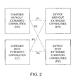
- a user may have access to different types of power converters and different types of electronic devices. Particularly in environments in which commonly available port connectors are used, a variety of different pairings between power converters and electronic devices are possible.
- FIG. 2 an environment of the type shown in FIG. 2 .
- a user may have access to two different types of power converter (type CR and type CE) and may have access to two different types of electronic device (type DR and type DE). This may lead to four possible pairings P1, P2, P3, and P4 between power converters and devices, as illustrated by the dashed line in FIG. 2 .
- Power converter CR may be compliant with industry standards (e.g., USB-IF standards) and may not have any extended capabilities beyond those specified by the industry standards. For example, power converter CR may only be able to produce voltages and currents that fall within the limits prescribed by the industry standards. Power converter CR may include a resistor with a value of less than 200 ohms that is connected between data lines DP and DN in power converter CR. The presence of this resistor may be used to advertise to electronic devices that power converter CR is compliant with USB-IF standards (or other such industry standards).
- industry standards e.g., USB-IF standards
- Power converter CE may have capabilities that extend beyond the limits imposed by the industry standards with which power converter CR complies. For example, power converter CE may be capable of delivering more DC power than power converter CR. Power converter CE may also have the capability to operate a lower voltages than converter CR (i.e., at voltages Vbus that are lower than permitted by the industry standards with which power converter CR complies).
- Examples of other extended capabilities that power converter CR may have include low-power-mode capabilities (i.e., capabilities to support sleep mode, hibernate mode, etc.), the ability to gather and store diagnostic information, the ability to accept power from an attached electronic device, the ability to upload diagnostic information to an attached device, the ability to support authentication operations, the ability to send and receive status information related to the power converter and electronic device operations, etc.).
- low-power-mode capabilities i.e., capabilities to support sleep mode, hibernate mode, etc.
- the ability to gather and store diagnostic information the ability to accept power from an attached electronic device, the ability to upload diagnostic information to an attached device, the ability to support authentication operations, the ability to send and receive status information related to the power converter and electronic device operations, etc.
- USB-IF standards may be silent with respect to gathering diagnostic information, but may set lower limits on the amount of voltage that a power converter may supply.
- a power converter that follows USB-IF standards may, for example, be required to supply 5 volts of output power at current levels of 0-0.5 A.
- Power converter CE may have the ability (in this example) to supply output powers of less than 5 volts at current levels of 0-0.5 A.
- Electronic device DR may be compliant with industry standards (e.g., USB-IF standards). In accordance with these standards, device DR may be configured to draw less than a maximum allowed amount of DC power from a charger. Device DE may have capabilities other than those permitted by the industry standards with which electronic device DR is compliant. Device DE may, for example, be capable of drawing more power from a charger than device DE (i.e., more power than permitted by the industry standards with which electronic device DR is compliant).
- power converter CE and device DE may use their control circuitry to detect when the use of extended capabilities is appropriate. If standards-compliant behavior is needed for compatibility, devices CE and DE can comply with the applicable standards. If devices CE and DE are connected to each other, there is no longer any need for maintaining standards compliance, so the extended capabilities of one or both of these items of equipment may be used.
- power converter CR presents a resistance R of less than 200 ohms between its DP and DN lines to indicate that power converter CR is a dedicated charger and is compliant with relevant industry standards (e.g., USB-IF standards).
- Device DR detects the presence of this resistance and operates accordingly by drawing as much power as permitted for a standards-compliant device that is connected to a standards-compliant dedicated charger.
- both power converter CR and device DR operate within prescribed bounds on current and voltage levels.
- Vbus is maintained above 5 volts and at currents of 0.5 to 1.5 A, Vbus is maintained above 2 volts. Currents above 1.5 A are not supplied by power converter CR and are not requested by device DR.
- power converter CR When power converter CR is connected to device DE (pairing P2), power converter CR will also present a resistance R of less than 200 ohms between its DP and DN lines to indicate that power converter CR is a dedicated charger and is compliant with relevant industry standards (e.g., USB-IF standards).
- Device DE may be a device such as electronic device 14 of FIG. 1 .
- device DE When connected to power converter CR, device DE may use control circuitry such as control circuitry 46 of FIG. 1 to measure the value of the resistance between the DP and DN contacts in power converter CR.
- device DE If device DE detects that the resistance across the DP and DN lines in power converter CR is less than 200 ohms and if device DE does not detect extended capabilities in power converter CR, device DE can conclude that power converter CR is compliant with industry standards (e.g. USB-IF standards) and can operate accordingly by drawing only as much power as permitted for a standards-compliant device that is connected to a standards-compliant dedicated charger.
- industry standards e.g. USB-IF standards
- Pairing P3 occurs when a power converter with extended (non-industry-standard) features (i.e., power converter CE) is connected to device DR.
- Power converter CE may, for example, be a power converter such as power converter 12 of FIG. 1 .
- power converter CE will uses its control circuitry (i.e.., circuitry 22 of FIG. 1 ) to present a resistance R of less than 200 ohms between its DP and DN lines. This indicates to device DR that power converter CE is able to function as a dedicated charger that is compliant with relevant industry standards (e.g., USB-IF standards).
- device DR can conclude that power converter CE is compliant with industry standards (e.g. USB-IF standards) and can operate accordingly by drawing only as much power as permitted for a standards-compliant device that is connected to a standards-compliant dedicated charger.
- industry standards e.g. USB-IF standards
- power converter CE will refrain from using extended capabilities that would violate the applicable industry standards. For example, power converter CE will refrain from supplying output voltages and currents in disallowed ranges.
- pairing P4 may arise when a power converter with extended (non-industry-standard) features (i.e., power converter CE) is connected to an electronic device with extended capabilities such as device DE.
- Power converter CE may be a power converter such as power converter 12 of FIG. 1 .
- Electronic device DE may be an electronic device such as electronic device 14 of FIG. 1 .
- power converter CE and device DE When power converter CE and device DE are connected, power converter CE and device DE may exchange information to signal to each other that they have extended capabilities.
- this type of information exchange may be primarily or exclusively unidirectional.
- power converter CE may actively or passively present information that is detectable by device DE that advertizes the presence of extended capabilities to device DE.
- control circuitry 22 may include a network of electrical components such as resistors, inductors, and capacitors that are connected between lines 24, 32, 30, and 28 (preferably in a way that does not interfere with the ability of power converter CE to present a shunt resistance R of less than 200 ohms across terminals DP and DN).
- power converter CE may present a capacitance C across DP and DN in parallel with the resistance R. At AC signal frequencies, this capacitor has a relative low resistance (i.e., the capacitor acts as a short circuit). The presence of the capacitor can therefore be detected by device DE by measuring the impedance between lines DP and DN at both DC and AC frequencies.
- Device DR can detect that the value of the shunt resistance is less than 200 ohms.
- Device DE can detect that R is less than 200 ohms (i.e., that R is 100 ohms) at DC and is lower at AC frequencies (e.g., at 1 kHz as an example).
- Other passive advertizing schemes may be used if desired.
- an inductor may be connected in series with the resistor R between terminals DP and DN so that a rise in impedance at AC frequencies can be detected, etc.
- control circuitry 22 may open and close a switch to modulate an electrical parameter.
- Control circuitry 22 may, for example, open and close a switch that is connected in series with a 100 ohm resistor between terminals DP and DN to modulate the resistance between terminal DP and DN.
- Control circuitry 22 may also generate voltage or current signals that are conveyed to device DE.
- Device DE may similarly use passive or active unidirectional advertising schemes to make the capabilities of device DE detectable by power converter CE.
- a network of detectable electrical components may be connected between lines 38, 40, 42, and 44, switching circuitry in communications circuitry 48 of control circuitry 46 may be used to modulate electrical parameters such as resistance, current, voltage, etc.
- both power converter CE and device DE may contain circuitry that is configured to passively or actively advertize their respective extended capabilities.
- control circuitry 22 and control circuitry 46 may each contain a USB communications circuit (e.g., a USB host or hub chip) or other suitable circuitry for conveying information (e.g., voltage sources, current sources, voltage detectors, current detectors, etc.).
- Any suitable modulation scheme (coding scheme) may be used when conveying information between power converter 12 and electronic device 14.
- modulation schemes include modulation schemes such as frequency modulation (FM) schemes, amplitude modulation (AM) schemes, pulse-code modulation (PCM) schemes, code-division-multiple-access (CDMA) schemes, phase-shift keying (PSK) schemes, and amplitude shift keying (ASK) schemes.
- FM frequency modulation
- AM amplitude modulation
- PCM pulse-code modulation
- CDMA code-division-multiple-access
- PSK phase-shift keying
- ASK amplitude shift keying
- the presence or absence of different AC frequencies (tones) may be used to represent information
- patterns of pulses may be used
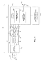
- FIG. 3 Illustrative circuitry that may be used to support communications in a power converter with extended capabilities such as power converter 12 of FIG. 1 and an electronic device with extended capabilities such as electronic device 14 is shown in FIG. 3 .
- power converter 12 may include control circuitry 24 and electronic device 14 may include control circuitry 46.
- control circuitry 24 and control circuitry 46 may include communications circuitry (e.g., communications circuit 60 in control circuit 58 of FIG. 3 and communications circuitry 48 in control circuitry 46 of FIG. 1 ) and may be based on one or more integrated circuits such as USB integrated circuits (host and hub controllers), microprocessors, digital signal processors, application-specific integrated circuits, etc.
- USB integrated circuits host and hub controllers
- microprocessors digital signal processors
- application-specific integrated circuits etc.
- This communications circuitry may generate control signals that are applied to control lines such as control line 64 of controllable current source 62, control line 66 of controllable switch 68, control line 78 of controllable voltage source 76, and control line 82 of controllable current source 80.
- Controllable components such as current sources 62 and 80, voltage source 76, and switching circuitry 68 are merely illustrative examples of components that may serve as transmitter circuitry for device 14 and that may be used in conveying modulated signals (e.g., signals that vary as a function of time and/or magnitude) between power converter 12 and electronic device 14.
- modulated signals e.g., signals that vary as a function of time and/or magnitude
- power converter 12 and device 14 need not include all of these components. These components are included in the diagram of FIG. 3 as an example.
- power converter 12 may present a resistance R (e.g., a resistance R of less than 200 ohms) between lines DP and DN to indicate to electronic devices that power converter 12 is capable of operating in compliance with industry standards (e.g., USB-IF standards) for stand-alone (dedicated) chargers. This may be done using resistor R of FIG. 3 .
- Optional series-connected switch 68 may normally be closed.
- device 14 may use current source 80 to apply a current to resistor R while using current sink 84 to sink returned current on line 42 to ground.
- the value of the resulting voltage V at input 90 of comparator 86 is compared by comparator 86 to reference voltage Vref at input 88 of comparator 86.
- Comparator 86 then produces a corresponding output signal (e.g., a logic high or low value) on output line 92.
- the value of voltage V on input 90 is indicative of the value of resistor R. If resistor R is less than 200 ohms, V will be less than Vref and output 92 will go high.
- resistor R is greater than 200 ohms (in this example), output 92 will be taken to a logic low value. If control circuitry 46 measures a high value at output 92, device 14 can therefore conclude that power converter 12 is at least capable of operating in compliance with industry standards (i.e., as a dedicated charger in compliance with USB-IF standards).
- Additional discovery operations may be performed by electronic device 14 to determine whether power converter 12 has extended capabilities (and vice versa). For example, electronic device 14 may issue a pattern of signal pulses (e.g., voltage pulses produced by modulating the voltage on voltage source 76 or current pulses produced by modulating the current produced by current source 80).
- Control circuitry 24 may use comparator 70 or other suitable detector (receiver) circuitry to receive the signal pulses transmitted by electronic device 14.
- Comparator 70 may have a first input (input 72) that receives reference voltage Vref2 and a second input (input 74) that receives signal pulses that have been transmitted by electronic device 14 (e.g., using current source 80, voltage source 76, or other signal transmitting circuitry).
- comparator 70 As incoming pulses are detected, the output of comparator 70 changes state and provides digital output pulses of correspondingly changing values to control circuit 58.
- comparator 70 serves as a receiver for signals transmitted by electronic device 14. If desired, receiver 70 may be sensitive to signals encoded using multiple different values (i.e., patterns of signals with different voltage values, patterns of signals with different current values, etc.).
- Power converter 12 can similarly transmit signals to electronic device 14.
- control circuit 58 may transmit current pulses to electronic device 14 (e.g., using current source 62) that are detected using comparator 86 or other suitable receiver circuitry in device 14, may transmit pulses by opening and closing switch 68 to modulate the resistance between lines 32 and 30 (e.g., so that device 14 can detect this change using current source 80 and comparator 86 or other suitable detection circuitry), etc.
- the signals that are transmitted from electronic device 14 and power converter 12 may be used to inform power converter 12 that electronic device 12 has extended capabilities, as described in connection with device DE of FIG. 2 .
- the signals that are transmitted from power converter 12 to electronic device 14 may be used to inform electronic device 14 that power converter 12 has extended capabilities, as described in connection with power converter CE of FIG. 2 .
- Transmitted signals may also be used for handshaking and to transmit status data, diagnostic data, control data, and other data between power converter 12 and device 14.
- power converter 12 may not be connected to line power, so power lines 38 and 44 may, if desired, be used to convey DC power from battery 52 ( FIG. 1 ) to control circuit 58 and the other circuitry of control circuitry 24. This allows power converter 12 to be operated even if AC-DC converter 20 is experiencing a fault.
- power converter 12 may use control circuitry 22 to periodically store status information (i.e., information on fault conditions, circuit health, etc.). This stored information may be organized in the form of a diagnostic log. If a fault occurs in AC-DC converter circuitry 20, electronic device 14 may be connected to power converter 12 to supply control circuitry 22 with power, even in the absence of DC power from AC-DC converter 20. Because control circuitry 22 can be powered in this way, control circuitry 22 may upload performance data from the diagnostic log once communications are established between power converter 12 and electronic device 14.
- status information i.e., information on fault conditions, circuit health, etc.
- the signaling techniques that are used to advertize and detect the presence of extended capabilities may be arranged so as not to interfere with standards-compliant detection protocols.
- the presence of extended capabilities may be advertized (e.g., using signal pulse codes) while remaining within voltage and current limits defined by industry standards.
- signal strength S (voltage, current, etc.) is plotted as a function of time.
- the components in system 8 i.e., power converter 12 and electronic device 14
- the signal S corresponds to a signal that is applied by one component in system 8 to the other when the components are paired.
- signal S may be a probe current that is applied across the DP and DN terminals in power converter 12 by electronic device 14 as electronic device 12 measures the value of R as described in connection with FIG. 3 .
- discovery period TD1 discovery period 1
- pulses PLS1 need no longer conform to limits S1 and S2 (i.e., signal S can exceed these limits). If desired, signal pulses PLS1 may also remain within limits S1 and S2.
- the coded information that is conveyed in pulses PLS1 (or other transmitted signal information S) may advertize to power converter 12 that electronic device 14 has extended capabilities or may contain other suitable data.
- the components of system 8 were able to convey information to each other on the presence of their extended capabilities while simultaneously ensuring standards compliance (i.e., by presenting resistor R across terminals DP and DN in the power converter and by respecting limits S1 and S2 while measuring the value of R with a probe current or other measurement signal).
- standards compliance i.e., by presenting resistor R across terminals DP and DN in the power converter and by respecting limits S1 and S2 while measuring the value of R with a probe current or other measurement signal.
- Another way to ensure that equipment with extended capabilities such as power converter CE and electronic device DE is able to interoperate with standards-compliant equipment involves using a delay period to avoid interference between standards-compliant discovery operations and communications associated with establishing and using extended capabilities.
- the strength of signal S (i.e., a probe current generated by current generator 80 of FIG. 3 ) is initially constant at a value that falls within specification limits S1 and S2.
- the standards-compliant discovery process in this type of arrangement will be completed within time TD1 after connecting power converter 12 and electronic device 14 at time t0.
- no changes may be made in the value of S until a delay time TD2 is complete.
- TD2 is greater than TD1
- changes to the value of S after TD2 will not fall within time period TD1 and will therefore not interfere with the standards-compliant discovery operations performed during time period TD1.
- signal S may therefore be modulated to form coded pulses PLS2 without regard to whether these signal pulses are within limits S1 and S2. Pulses PLS2 may be modulated in time, in magnitude, etc.
- a user connects a power converter and electronic device.
- the power converter may be plugged into a source of line power or may be operated with battery power supplied by the electronic device.
- USB connectors or other connectors may be used to interconnect the power converter and electronic device.
- the power converter and electronic device may only have capabilities that comply with industry standards (e.g., USB-IF standards for dedicated chargers) as described in connection with power converter CR and electronic device DR of FIG. 2 or may have extended capabilities as described in connection with power converter CE and electronic device DE. Different pairings between devices are possible.
- industry standards e.g., USB-IF standards for dedicated chargers
- the power converter may include a resistor R of less than 200 ohms across its DP and DN terminals.
- device DR applies a probe signal across the DP and DN terminals and measures that R is less than 200 ohms.
- power converter CR and device DR may operate according to industry standards (e.g., USB-IF standards for dedicated chargers).
- power converter CR may power device DR and charge the battery in device DR in compliance with voltage and current limits specified in the industry standards.
- device DE may, at step 100, use schemes of the type described in connection with FIGS. 4 and 5 to detect the presence of a resistor R of less than 200 ohms across the DP and DN terminals, while also advertising the extended capabilities of electronic device DE (e.g., by transmitting a coded set of current pulses to power converter CR).
- Power converter CR (in this example) does not have extended capabilities, so power converter CR does not respond to the advertized extended capabilities of device DE.
- power converter CR and device DE may operate according to industry standards (e.g., USB-IF standards for dedicated chargers).
- power converter CR may power device DE and charge the battery in device DE in compliance with voltage and current limits specified in the industry standards.
- charger CE may, at step 102, use schemes of the type described in connection with FIGS. 4 and 5 to advertize the presence of its extended capabilities while presenting a resistor R of less than 200 ohms across the DP and DN terminals to indicate to electronic device DR that power converter CE is able to operate according to industry standards (i.e., USB-IF dedicated charger standards).
- Industry standards i.e., USB-IF dedicated charger standards.
- Device DR does not have extended capabilities, so device DR does not respond to the transmission of the signals from power converter CE that advertize the presence of extended capabilities.
- power converter CE and device DR may therefore operate according to industry standards (e.g., USB-IF standards for dedicated chargers).
- a user will connect a power converter with extended capabilities (power converter CE) to a device with extended capabilities (device DE) at step 94.
- power converter CE may, in this type of situation, present a resistance R of less than 200 ohms across terminals DP and DN to indicate that power converter CE can comply with industry standards (i.e., USB-IF dedicated charger standards).
- Power converter CE and device DE may also communicate using signal pulses or other communications schemes (e.g., schemes of the type described in connection with FIGS. 3 , 4, and 5 ). These signals may allow power converter CE to advertize its extended capabilities to device DE and may allow device DE to advertize its extended capabilities to power converter CE.
- power converter CE and device DE may use their extended capabilities (step 106).
- the extended capabilities that are used during the operations of step 106 may involve the delivery of amounts of current and voltage between power converter CE and device DE that are outside of industry specifications (i.e., that are above or below values permitted by USB-IF dedicated charger standards or other industry standards).
- power converter CE can deliver a voltage that is below the minimum required output voltage level for Vbus at a given current (i.e., 4.5 volts at 0.3 A). The use of this lowered voltage may help power converter CE conserve power when the full voltage level of Vbus is not required.
- power converter CE can deliver more current and voltage than permitted by the industry standards (i.e., a voltage of 6 volts and a current of 3 A). This allows power converter CE to deliver enlarged amounts of power to device DE (e.g., to support power-hungry operations, to shorten charging times, etc.). Data may also be exchanged between power converter CE and device DE during the operations of step 106 (e.g., diagnostics data from a log on power converter CE, status information, etc.). If desired, device DE may deliver power to power converter CE over power lines VBUS and GND (e.g., to allow power converter CE to function even in the event that AC-DC converter 20 is exhibiting a failure). Data may be exchanged using coded pulses or other suitable communications schemes.
- a power converter in accordance with an embodiment, includes first and second power lines, an alternating current (AC) to direct current (DC) converter circuit that applies a DC power supply voltage across the first and second power lines, first and second data lines, and control circuitry that includes a resistor that is coupled across the first and second data lines, wherein the control circuitry includes detector circuitry that detects modulated signals on at least one of the first and second data lines.
- AC alternating current
- DC direct current
- a power converter wherein the control circuitry includes receiver circuitry coupled to at least one of the data lines.
- a power converter wherein the receiver circuitry includes a comparator having a first input connected to the second data line and having a second input that receives a reference voltage.
- a power converter wherein the resistor has a resistance value of less than 200 ohms.
- a power converter wherein the resistor has a first terminal connected to the second data line and has a second terminal and wherein the control circuitry includes a switch connected between the second terminal of the resistor and the first data line.
- a power converter wherein the control circuitry includes an adjustable current source having an output connected to one of the data lines.
- a power converter that also includes first, second, third, and fourth Universal Serial Bus contacts, wherein the first contact includes a positive power supply contact and is connected to the first power line, wherein the fourth contact includes a ground power supply contact and is connected to the second power line, wherein the second contact is a positive data line contact and is connected to the first data line, and wherein the second contact is a negative data line contact and is connected to the second data line.
- an electronic device in accordance with an embodiment, includes a connector having a pair of power line contacts and a pair of data line contacts, and control circuitry that measures how much resistance exists between the pair of data line contacts using a signal, wherein the control circuitry includes transmitter circuitry that transmits data by modulating the signal to create signal pulses.
- an electronic device wherein the power line contacts include Universal Serial Bus power line contacts and wherein the data line contacts includes Universal Serial Bus data line connectors.
- an electronic device wherein the transmitter circuitry includes a current source and wherein the control circuitry is configured to hold the signal constant when measuring how much resistance exists between the pair of data line contacts.
- an electronic device wherein the data line contacts include a first data line contact and a second data line contact, wherein the transmitter circuitry includes a current source that is connected to the first data line contact, wherein the signal includes a probe current that is held constant when the control circuitry measures how much resistance exists between the pair of data lines, and wherein the signal pulses include current pulses.
- control circuitry further includes a current sink that receives current from the second data line contact.
- an electronic device wherein the transmitter circuitry includes a voltage source connected to one of the data line contacts.
- an electronic device wherein the data line contacts include a first data line contact and a second data line contact, wherein the transmitter circuitry includes a current source that is connected to the first data line contact, wherein the signal includes a probe current that varies as a function of time while the control circuitry measures how much resistance exists between the pair of data lines.
- control circuitry includes receiver circuitry that receives data signal pulses from external equipment using at least one of the data line contacts.
- a method for operating an alternating current (AC) to direct current (DC) power converter that supplies power to an electronic device to which the power converter is connected using a port that includes first and second power supply lines and first and second data lines, the method including receiving a signal from the electronic device using the first and second data lines, routing the signal through a resistor in the power converter that is connected between the first and second data lines, and with a receiver in the power converter, receiving a plurality of pulsed data signals from the electronic device.
- AC alternating current
- DC direct current
- receiving the plurality of pulses data signals includes using a comparator to receive the pulsed data signals.
- a method that also includes transmitting data signals from the power converter to the electronic device using at least one of the data lines.
- transmitting the data signals includes modulating a current source that has an output connected to one of the data lines.
- transmitting the data signals includes opening and closing a switch that is connected in series with the resistor to modulate how much resistance is present between the first and second data lines.
Abstract
Description
- This application claims priority to United States patent application No.
12/766,840, filed April 23, 2010 - This relates to systems in which power converters are used to charge electronic devices.
- Power converter circuitry can be used to convert alternating current (AC) power into direct current (DC) power. AC power is typically supplied from wall outlets and is sometimes referred to as line power. Electronic devices include circuitry that runs from DC power. The DC power that is created by an AC-to-DC power converter may be used to power an electronic device. The DC power that is created may also be used to charge a battery in an electronic device.
- Some electronic devices have input-output ports that include power and data lines. For example, some electronic devices have input-output ports such as Universal Serial Bus ports that include a pair of power lines and a pair of data lines. Universal Serial Bus (USB) connectors and other connectors may be used in ports such as these.
- During normal operation of an electronic device, the USB port of a device may be used to convey power and data signals. For example, the USB port may be used to power a peripheral such as a printer or camera, to transfer data to and from an accessory, etc. Devices with batteries may be charged by drawing DC power from the power lines in the USB port. For example, a battery in a cellular telephone may be charged when the cellular telephone is connected to a USB port of a computer.
- It can be convenient to charge electronic devices using USB ports on computers, but computer ports such as these are designed to supply only a limited amount of power. Faster charging can be achieved using stand-alone power converters. Stand-alone power converters can be provided with cables that have Universal Serial Bus plugs. This type of USB plug may be inserted into a Universal Serial Bus port on an electronic device, allowing the device to be charged from a wall outlet without involving a computer.
- Although stand-alone USB chargers such as these may offer more charging power than the USB port on a computer, the capabilities of stand-alone USB chargers and other aspects of USB-based charging systems may be limited by industry standards.
- It would therefore be desirable to be able to provide improved charging systems such as charging systems in which power is conveyed over input-output port paths such as Universal Serial Bus paths.
- To comply with industry standards, an alternating current (AC) to direct current (DC) power converter and electronic device may conform to expected discovery protocols. The power converter and electronic device may be connected using connectors that have a pair of power lines and a pair of data lines such as a Universal Serial Bus connector. The power converter may include a resistor across its data lines. During discovery operations, the electronic device may generate a probe signal such as a probe current that is routed through the resistor. The electronic device may use the probe signal to measure the resistance of the resistor in the power converter.
- In addition to standards-compliant capabilities, the AC-DC power converter and the electronic device may have extended capabilities. These extended capabilities may include features that support enhanced power transfer capabilities, data transfer capabilities to support the transfer of status and diagnostic data, and other functions.
- The AC-DC power converter and the electronic device may support standards-compliant discovery operations such as operations related to presenting and detecting the resistor across the data lines. During these discovery operations or after a delay, the AC-DC power converter and electronic device may exchange additional modulated signals. These modulated signals may take the form of current pulses, voltage pulses or other signals that are modulated as a function of time and/or magnitude. Transmitter circuitry and corresponding receiver circuitry may be used in the power converter and in the electronic device to support unidirectional and bidirectional communications. The transmitter circuitry may be based on current sources, voltage sources, switches, or other circuit components that are modulated using communications circuitry. The receiver circuitry may include comparators and other receiver circuits that convert transmitted signals into received data.
- When a power converter or electronic device with extended capabilities is connected to equipment without extended capabilities, the extended-capability equipment reverts to standards-compliant behavior, thereby preserving compatibility between a variety of equipment.
- Further features of the invention, its nature and various advantages will be more apparent from the accompanying drawings and the following detailed description of the preferred embodiments.
-
-
FIG. 1 is a circuit diagram of a system including a power converter and an electronic device in accordance with an embodiment of the present invention. -
FIG. 2 is a diagram showing how chargers and electronic devices with different levels of charging capabilities and other capabilities may be interconnected in a variety of pairings in accordance with an embodiment of the present invention. -
FIG. 3 is a circuit diagram of an illustrative charger and electronic device in accordance with an embodiment of the present invention. -
FIG. 4 is a graph showing an illustrative signaling pattern that may be used to convey information between a device of the type shown inFIG. 3 and a charger of the type shown inFIG. 3 in accordance with an embodiment of the present invention. -
FIG. 5 is a graph showing another illustrative signaling pattern that may be used to convey information between a charger of the type shown inFIG. 3 and an electronic device of the type shown inFIG. 3 in accordance with an embodiment of the present invention. -
FIG. 6 is a flow chart of illustrative steps involved in operating a system that includes a power converter of the type shown inFIG. 1 and an electronic device of the type shown inFIG. 3 in accordance with an embodiment of the present invention. - Power converters (sometimes referred to as power adapters) may be used to convert alternating current (AC) power into direct current (DC) power. A power converter may have a plug that plugs into a wall socket to obtain AC line power. The power converter may also have an output path on which DC power is provided that has been created from the AC line power. In some situations, AC-DC power converter circuitry may be built into computers and other electronic equipment. In other situations, AC-DC power converter circuitry is used to form stand-alone power converters. Charging systems that include stand-alone power converters are sometimes described herein as an example.
- Power converters can be used to power electronic devices that use DC power. In a device that contains a rechargeable battery, DC power from a power converter can also be used to charge the battery. In this type of situation, an AC-DC power converter can serve as a stand-alone charger. AC-DC power converters are therefore sometimes referred to as battery chargers.
- Industry standards may place limits on the behavior of power converters and the electronic devices that are powered by the power converters. For example, industry standards may dictate that stand-alone (dedicated) Universal Serial Bus (USB) chargers present a shunt resistance of less than 200 ohms across their data lines. According to industry standard protocols, the presence of this resistance can be detected by an attached electronic device. When detected, the electronic device can conclude that a dedicated charger is present and can draw more power than would otherwise be available through a computer-based USB port. Although industry standards may allow the stand-alone charger to charge a battery in an electronic device more rapidly than would be possible using a computer-based USB port, these standards may also place limits on the maximum power that a stand-alone charger can deliver and limits on the maximum power that an electronic device can draw from the charger. Limits of this type may undesirably restrict the use of the charger and electronic device.
- These shortcomings can be addressed using a charging system of the type shown in
FIG. 1 . As shown inFIG. 1 , chargingsystem 8 may include a source of line power such as alternating current (AC)source 16, a power converter such as stand-alone (dedicated)charger 12, and an electronic device such asdevice 14. -
AC source 16 may be, for example, a wall outlet or other AC power source.Power converter 12 may convert AC power fromsource 16 to direct-current (DC) power for poweringelectronic device 14.Electronic device 14 may be a portable electronic device such as a cellular telephone, tablet computer, notebook computer, media player, gaming device, remote control, or other electronic equipment. -
Power converter 12 may have a plug that mates with a corresponding wall outlet (shown asmating connectors 18 inFIG. 1 ). This supplies AC power to AC-DC converter circuitry 20. AC-DC converter circuitry 20 may be based on a switched-mode AC-DC converter circuit and may supply DC power onpower lines DC converter circuit 20 may supply a positive power supply voltage Vbus (e.g., 2-5 volts, less than 2 volts, more than 5 volts, etc.) on positivepower supply line 24 and may supply a ground voltage GND (e.g., a signal at 0 volts) or groundpower supply line 28. -
Converter 12 may have a permanently connected cable or may have a detachable cable that is terminated in a connector such as a USB connector (e.g., a USB plug). This connector may have a number of contacts that make electrical contact with corresponding contacts in a connector ondevice 14. - As shown in
FIG. 1 ,power converter 12 may have a four-contact USB connector (connector 34) that includes a VBUS contact, data line contacts DP and DN, and a GND contact. The VBUS contact inconnector 34 is electrically connected to positivepower supply line 24. The GND contact inconnector 34 is electrically connected to groundline 28.Lines power converter 12 are electrically connected to the DP and DN contacts inconnector 34, respectively. -
Device 14 may likewise have a four-contact USB connector (connector 36) that includes a VBUS contact connected to positive power supply line 38 (e.g., to carry voltage VBUS), data line contacts DP and DN that are respectively connected to DP and DN data lines 40 and 42, and a GND contact connected to groundline 42.Connectors - The VBUS contact in
connector 36 and the GND contact inconnector 36 and correspondingpower supply lines power converter 12 to the circuitry of device 14 (e.g., to power device 14).Device 14 can also be powered using an internal battery such asbattery 52.Battery 52 may be a rechargeable battery such as a lithium-ion battery.Battery 52 may be coupled betweenpower management circuit 50 incontrol circuitry 46 andground 54. Whenbattery 52 is fully charged anddevice 14 is running from battery power,power management circuit 50 can be used to deliver battery power to the circuitry ofdevice 14 andpower converter 12. Whenbattery 52 is depleted and DC power is available frompower converter 12 onlines power management circuit 50 can be used to chargebattery 52 with the DC power. -
Device 14 may include input-output circuitry andother components 56 andcontrol circuitry 46 that includespower management circuit 50 andcommunications circuitry 48. Input-output circuitry andother components 56 may include buttons, displays, speakers, microphones, sensors, and other electronic components.Control circuitry 46 may be based on one or more integrated circuits (e.g., memory chips, audio and video integrated circuits, microprocessors, digital signal processors, application-specific integrated circuits, etc.). - During normal operation of
device 14,connector 36 and associatedpower lines data lines device 14 is connected to a peripheral,device 14 may use the power lines to supply power to the peripheral and may use the data lines to support bidirectional communications with the accessory. - When connected to
power adapter 12,device 14 andpower adapter 12 may interact with each other to determine each other's capabilities. In a conventional dedicated charger that is compliant with USB-IF standards, a resistor of less than 200 ohms is connected between the DP and DN lines in the charger. The presence of this shunt resistor serves as a flag that informs connected devices that the charger is a dedicated charger and not a USB computer port.Power converter 12 ofFIG. 1 can replicate this behavior usingcontrol circuitry 22 when needed. This allowspower converter 12 to serve as a standards-compliant charger (e.g., a USB-IF dedicated charger) when desired (i.e., when interacting with devices that are only capable of standards-compliant operation). When a device such asdevice 14 ofFIG. 1 that has extended capabilities (i.e., capabilities beyond the capabilities defined by applicable industry standards such as USB-IF standards),power converter 12 anddevice 14 can exhibit enhanced capabilities. - As shown in
FIG. 1 ,control circuitry 22 may be connected to the DP and DN data line connectors inconnector 34 bydata lines Control circuitry 22 may be coupled to AC-DC converter circuit 20 bycontrol path 26.Control path 26 may be used to issue commands to AC-DC converter (e.g., so thatcontrol circuitry 22 may place AC-DC converter 20 in a sleep mode and so thatcontrol circuitry 22 may awaken AC-DC converter circuit 20 from sleep mode).Control circuitry 22 may also be coupled to positivepower supply line 24 andground line 28. -
Control circuitry 22 may include a resistive element such as a resistor with a value of less than 200 ohms and may contain switching circuitry that selectively connects this resistive element in a shunt resistor configuration bridgingdata lines power converter 12 can determine thatconverter 12 is capable of serving as a dedicated charger (i.e., as a charger that is compliant with industry standards such as USB-IF standards).Control circuitry 22 may also include communications circuitry that supports communications withcommunications circuitry 48 ofdevice 14. - The communications circuitry in
control circuitry 22 andcontrol circuitry 46 may use unidirectional signaling schemes (i.e., schemes in which capabilities are advertized exclusively or primarily in one direction) and bidirectional signaling schemes (i.e., communications schemes in which information is exchanged betweenpower converter 12 anddevice 14 in both directions). In bidirectional signaling schemes, features such as handshaking may be implemented. Communications betweenpower converter 12 anddevice 14 may be implemented using any suitable type of protocols (e.g., USB protocols, less complex protocols, more complex protocols, etc.). - Users may have access to different types of power converters and different types of electronic devices. Particularly in environments in which commonly available port connectors are used, a variety of different pairings between power converters and electronic devices are possible. Consider, for example, an environment of the type shown in
FIG. 2 . As shown inFIG. 2 , a user may have access to two different types of power converter (type CR and type CE) and may have access to two different types of electronic device (type DR and type DE). This may lead to four possible pairings P1, P2, P3, and P4 between power converters and devices, as illustrated by the dashed line inFIG. 2 . - Power converter CR may be compliant with industry standards (e.g., USB-IF standards) and may not have any extended capabilities beyond those specified by the industry standards. For example, power converter CR may only be able to produce voltages and currents that fall within the limits prescribed by the industry standards. Power converter CR may include a resistor with a value of less than 200 ohms that is connected between data lines DP and DN in power converter CR. The presence of this resistor may be used to advertise to electronic devices that power converter CR is compliant with USB-IF standards (or other such industry standards).
- Power converter CE may have capabilities that extend beyond the limits imposed by the industry standards with which power converter CR complies. For example, power converter CE may be capable of delivering more DC power than power converter CR. Power converter CE may also have the capability to operate a lower voltages than converter CR (i.e., at voltages Vbus that are lower than permitted by the industry standards with which power converter CR complies). Examples of other extended capabilities that power converter CR may have include low-power-mode capabilities (i.e., capabilities to support sleep mode, hibernate mode, etc.), the ability to gather and store diagnostic information, the ability to accept power from an attached electronic device, the ability to upload diagnostic information to an attached device, the ability to support authentication operations, the ability to send and receive status information related to the power converter and electronic device operations, etc.).
- The industry standards with which power converter CR is compliant may be silent with respect to some of the extended features of power converter CE, but may actively prohibit use of other extended features. For example, USB-IF standards may be silent with respect to gathering diagnostic information, but may set lower limits on the amount of voltage that a power converter may supply. A power converter that follows USB-IF standards may, for example, be required to supply 5 volts of output power at current levels of 0-0.5 A. Power converter CE may have the ability (in this example) to supply output powers of less than 5 volts at current levels of 0-0.5 A.
- Electronic device DR may be compliant with industry standards (e.g., USB-IF standards). In accordance with these standards, device DR may be configured to draw less than a maximum allowed amount of DC power from a charger. Device DE may have capabilities other than those permitted by the industry standards with which electronic device DR is compliant. Device DE may, for example, be capable of drawing more power from a charger than device DE (i.e., more power than permitted by the industry standards with which electronic device DR is compliant).
- In order to ensure interoperability with standards-compliant equipment such as power converter CR and device DR, power converter CE and device DE may use their control circuitry to detect when the use of extended capabilities is appropriate. If standards-compliant behavior is needed for compatibility, devices CE and DE can comply with the applicable standards. If devices CE and DE are connected to each other, there is no longer any need for maintaining standards compliance, so the extended capabilities of one or both of these items of equipment may be used.
- The way in which the power converters and electronic devices of
FIG. 2 operate depends on how they are paired. Consider, as an example, a situation in which power converter CR is connected to device DR (pairing P1). In this situation, power converter CR presents a resistance R of less than 200 ohms between its DP and DN lines to indicate that power converter CR is a dedicated charger and is compliant with relevant industry standards (e.g., USB-IF standards). Device DR detects the presence of this resistance and operates accordingly by drawing as much power as permitted for a standards-compliant device that is connected to a standards-compliant dedicated charger. Following the limits of the industry standards, both power converter CR and device DR operate within prescribed bounds on current and voltage levels. For example, at currents of 0-0.5 A, Vbus is maintained above 5 volts and at currents of 0.5 to 1.5 A, Vbus is maintained above 2 volts. Currents above 1.5 A are not supplied by power converter CR and are not requested by device DR. - When power converter CR is connected to device DE (pairing P2), power converter CR will also present a resistance R of less than 200 ohms between its DP and DN lines to indicate that power converter CR is a dedicated charger and is compliant with relevant industry standards (e.g., USB-IF standards). Device DE may be a device such as
electronic device 14 ofFIG. 1 . When connected to power converter CR, device DE may use control circuitry such ascontrol circuitry 46 ofFIG. 1 to measure the value of the resistance between the DP and DN contacts in power converter CR. If device DE detects that the resistance across the DP and DN lines in power converter CR is less than 200 ohms and if device DE does not detect extended capabilities in power converter CR, device DE can conclude that power converter CR is compliant with industry standards (e.g. USB-IF standards) and can operate accordingly by drawing only as much power as permitted for a standards-compliant device that is connected to a standards-compliant dedicated charger. - Pairing P3 occurs when a power converter with extended (non-industry-standard) features (i.e., power converter CE) is connected to device DR. Power converter CE may, for example, be a power converter such as
power converter 12 ofFIG. 1 . When power converter CE and device DR are connected, power converter CE will uses its control circuitry (i.e..,circuitry 22 ofFIG. 1 ) to present a resistance R of less than 200 ohms between its DP and DN lines. This indicates to device DR that power converter CE is able to function as a dedicated charger that is compliant with relevant industry standards (e.g., USB-IF standards). Once device DR detects that the resistance across the DP and DN lines in power converter CE is less than 200 ohms, device DR can conclude that power converter CE is compliant with industry standards (e.g. USB-IF standards) and can operate accordingly by drawing only as much power as permitted for a standards-compliant device that is connected to a standards-compliant dedicated charger. In the absence of additional information that indicates to power converter CE that the attached electronic device has extended capabilities, power converter CE will refrain from using extended capabilities that would violate the applicable industry standards. For example, power converter CE will refrain from supplying output voltages and currents in disallowed ranges. - In pairings such as pairing P4, a charger with extended capabilities may be connected to an electronic device with extended capabilities. In particular, pairing P4 may arise when a power converter with extended (non-industry-standard) features (i.e., power converter CE) is connected to an electronic device with extended capabilities such as device DE. Power converter CE may be a power converter such as
power converter 12 ofFIG. 1 . Electronic device DE may be an electronic device such aselectronic device 14 ofFIG. 1 . - When power converter CE and device DE are connected, power converter CE and device DE may exchange information to signal to each other that they have extended capabilities.
- With one suitable arrangement, this type of information exchange may be primarily or exclusively unidirectional. As an example, power converter CE may actively or passively present information that is detectable by device DE that advertizes the presence of extended capabilities to device DE.
- With passive advertizing approaches,
control circuitry 22 may include a network of electrical components such as resistors, inductors, and capacitors that are connected betweenlines - With active advertizing approaches,
control circuitry 22 may open and close a switch to modulate an electrical parameter.Control circuitry 22 may, for example, open and close a switch that is connected in series with a 100 ohm resistor between terminals DP and DN to modulate the resistance between terminal DP and DN.Control circuitry 22 may also generate voltage or current signals that are conveyed to device DE. - Device DE may similarly use passive or active unidirectional advertising schemes to make the capabilities of device DE detectable by power converter CE. For example, a network of detectable electrical components may be connected between
lines communications circuitry 48 ofcontrol circuitry 46 may be used to modulate electrical parameters such as resistance, current, voltage, etc. - If desired, both power converter CE and device DE may contain circuitry that is configured to passively or actively advertize their respective extended capabilities.
- Bidirectional communications between power converter CE and electrical device DE may also be supported. For example,
control circuitry 22 andcontrol circuitry 46 may each contain a USB communications circuit (e.g., a USB host or hub chip) or other suitable circuitry for conveying information (e.g., voltage sources, current sources, voltage detectors, current detectors, etc.). Any suitable modulation scheme (coding scheme) may be used when conveying information betweenpower converter 12 andelectronic device 14. Examples of modulation schemes that may be used include modulation schemes such as frequency modulation (FM) schemes, amplitude modulation (AM) schemes, pulse-code modulation (PCM) schemes, code-division-multiple-access (CDMA) schemes, phase-shift keying (PSK) schemes, and amplitude shift keying (ASK) schemes. As an example, the presence or absence of different AC frequencies (tones) may be used to represent information, patterns of pulses may be used to represent information, etc. - Illustrative circuitry that may be used to support communications in a power converter with extended capabilities such as
power converter 12 ofFIG. 1 and an electronic device with extended capabilities such aselectronic device 14 is shown inFIG. 3 . As shown inFIG. 3 ,power converter 12 may includecontrol circuitry 24 andelectronic device 14 may includecontrol circuitry 46. As described in connection withFIG. 1 ,control circuitry 24 andcontrol circuitry 46 may include communications circuitry (e.g.,communications circuit 60 incontrol circuit 58 ofFIG. 3 andcommunications circuitry 48 incontrol circuitry 46 ofFIG. 1 ) and may be based on one or more integrated circuits such as USB integrated circuits (host and hub controllers), microprocessors, digital signal processors, application-specific integrated circuits, etc. This communications circuitry may generate control signals that are applied to control lines such ascontrol line 64 of controllablecurrent source 62,control line 66 ofcontrollable switch 68,control line 78 ofcontrollable voltage source 76, and controlline 82 of controllablecurrent source 80. Controllable components such ascurrent sources voltage source 76, and switchingcircuitry 68 are merely illustrative examples of components that may serve as transmitter circuitry fordevice 14 and that may be used in conveying modulated signals (e.g., signals that vary as a function of time and/or magnitude) betweenpower converter 12 andelectronic device 14. Moreover,power converter 12 anddevice 14 need not include all of these components. These components are included in the diagram ofFIG. 3 as an example. - It may be desirable for
power converter 12 to present a resistance R (e.g., a resistance R of less than 200 ohms) between lines DP and DN to indicate to electronic devices thatpower converter 12 is capable of operating in compliance with industry standards (e.g., USB-IF standards) for stand-alone (dedicated) chargers. This may be done using resistor R ofFIG. 3 . Optional series-connectedswitch 68 may normally be closed. - During an initial discovery process (i.e., when
switch 68 is closed),device 14 may usecurrent source 80 to apply a current to resistor R while usingcurrent sink 84 to sink returned current online 42 to ground. The value of the resulting voltage V atinput 90 ofcomparator 86 is compared bycomparator 86 to reference voltage Vref atinput 88 ofcomparator 86.Comparator 86 then produces a corresponding output signal (e.g., a logic high or low value) onoutput line 92. The value of voltage V oninput 90 is indicative of the value of resistor R. If resistor R is less than 200 ohms, V will be less than Vref andoutput 92 will go high. If resistor R is greater than 200 ohms (in this example),output 92 will be taken to a logic low value. Ifcontrol circuitry 46 measures a high value atoutput 92,device 14 can therefore conclude thatpower converter 12 is at least capable of operating in compliance with industry standards (i.e., as a dedicated charger in compliance with USB-IF standards). - Additional discovery operations may be performed by
electronic device 14 to determine whetherpower converter 12 has extended capabilities (and vice versa). For example,electronic device 14 may issue a pattern of signal pulses (e.g., voltage pulses produced by modulating the voltage onvoltage source 76 or current pulses produced by modulating the current produced by current source 80).Control circuitry 24 may usecomparator 70 or other suitable detector (receiver) circuitry to receive the signal pulses transmitted byelectronic device 14.Comparator 70 may have a first input (input 72) that receives reference voltage Vref2 and a second input (input 74) that receives signal pulses that have been transmitted by electronic device 14 (e.g., usingcurrent source 80,voltage source 76, or other signal transmitting circuitry). As incoming pulses are detected, the output ofcomparator 70 changes state and provides digital output pulses of correspondingly changing values to controlcircuit 58. In this respect,comparator 70 serves as a receiver for signals transmitted byelectronic device 14. If desired,receiver 70 may be sensitive to signals encoded using multiple different values (i.e., patterns of signals with different voltage values, patterns of signals with different current values, etc.). -
Power converter 12 can similarly transmit signals toelectronic device 14. For example,control circuit 58 may transmit current pulses to electronic device 14 (e.g., using current source 62) that are detected usingcomparator 86 or other suitable receiver circuitry indevice 14, may transmit pulses by opening and closingswitch 68 to modulate the resistance betweenlines 32 and 30 (e.g., so thatdevice 14 can detect this change usingcurrent source 80 andcomparator 86 or other suitable detection circuitry), etc. - The signals that are transmitted from
electronic device 14 andpower converter 12 may be used to informpower converter 12 thatelectronic device 12 has extended capabilities, as described in connection with device DE ofFIG. 2 . Similarly, the signals that are transmitted frompower converter 12 toelectronic device 14 may be used to informelectronic device 14 thatpower converter 12 has extended capabilities, as described in connection with power converter CE ofFIG. 2 . Transmitted signals may also be used for handshaking and to transmit status data, diagnostic data, control data, and other data betweenpower converter 12 anddevice 14. In some circumstances,power converter 12 may not be connected to line power, sopower lines FIG. 1 ) to controlcircuit 58 and the other circuitry ofcontrol circuitry 24. This allowspower converter 12 to be operated even if AC-DC converter 20 is experiencing a fault. - To facilitate troubleshooting,
power converter 12 may usecontrol circuitry 22 to periodically store status information (i.e., information on fault conditions, circuit health, etc.). This stored information may be organized in the form of a diagnostic log. If a fault occurs in AC-DC converter circuitry 20,electronic device 14 may be connected topower converter 12 to supplycontrol circuitry 22 with power, even in the absence of DC power from AC-DC converter 20. Becausecontrol circuitry 22 can be powered in this way,control circuitry 22 may upload performance data from the diagnostic log once communications are established betweenpower converter 12 andelectronic device 14. - To ensure that equipment with extended capabilities such as power converter CE and electronic device DE is able to interoperate with standards-compliant equipment, the signaling techniques that are used to advertize and detect the presence of extended capabilities may be arranged so as not to interfere with standards-compliant detection protocols. For example, the presence of extended capabilities may be advertized (e.g., using signal pulse codes) while remaining within voltage and current limits defined by industry standards.
- An example of this type of signaling scheme is shown in the graph of
FIG. 4 . In the graph ofFIG. 4 , signal strength S (voltage, current, etc.) is plotted as a function of time. The components in system 8 (i.e.,power converter 12 and electronic device 14) are connected to each other by plugging in their USB connectors or other suitable connectors at time to. The signal S corresponds to a signal that is applied by one component insystem 8 to the other when the components are paired. As just one example, signal S may be a probe current that is applied across the DP and DN terminals inpower converter 12 byelectronic device 14 aselectronic device 12 measures the value of R as described in connection withFIG. 3 . Industry standards may require that the value of the probe current fall within certain limits (shown as lower signal magnitude limit S1 and upper signal magnitude limit S2 in the example ofFIG. 4 ). To ensure that industry standards are not violated during the discovery process, signal S may remain within these limits. However, rather than using a DC signal that remains within specified limits S1 and S2, signal S may be modulated (varied in time and/or magnitude). - Industry standards may specify that discovery operations such as the measurement of the value of resistor R take place within a particular time frame (shown schematically as discovery period TD1). Once discovery period TD1 is complete, pulses PLS1 need no longer conform to limits S1 and S2 (i.e., signal S can exceed these limits). If desired, signal pulses PLS1 may also remain within limits S1 and S2. The coded information that is conveyed in pulses PLS1 (or other transmitted signal information S) may advertize to
power converter 12 thatelectronic device 14 has extended capabilities or may contain other suitable data. - In the example of
FIG. 4 , the components ofsystem 8 were able to convey information to each other on the presence of their extended capabilities while simultaneously ensuring standards compliance (i.e., by presenting resistor R across terminals DP and DN in the power converter and by respecting limits S1 and S2 while measuring the value of R with a probe current or other measurement signal). Another way to ensure that equipment with extended capabilities such as power converter CE and electronic device DE is able to interoperate with standards-compliant equipment, involves using a delay period to avoid interference between standards-compliant discovery operations and communications associated with establishing and using extended capabilities. - This type of approach is illustrated in the example of
FIG. 5 . InFIG. 5 , the strength of signal S (i.e., a probe current generated bycurrent generator 80 ofFIG. 3 ) is initially constant at a value that falls within specification limits S1 and S2. The standards-compliant discovery process in this type of arrangement will be completed within time TD1 after connectingpower converter 12 andelectronic device 14 at time t0. To ensure that changes to the value of probe signal S do not adversely affect compliance with industry standards, no changes may be made in the value of S until a delay time TD2 is complete. Because TD2 is greater than TD1, changes to the value of S after TD2 will not fall within time period TD1 and will therefore not interfere with the standards-compliant discovery operations performed during time period TD1. After time period TD2 has elapsed, signal S may therefore be modulated to form coded pulses PLS2 without regard to whether these signal pulses are within limits S1 and S2. Pulses PLS2 may be modulated in time, in magnitude, etc. - Illustrative steps involved in operating power converters and electronic devices in various pairings of the type described in connection with
FIG. 2 are shown inFIG. 6 . Atstep 94, a user connects a power converter and electronic device. The power converter may be plugged into a source of line power or may be operated with battery power supplied by the electronic device. USB connectors or other connectors may be used to interconnect the power converter and electronic device. - The power converter and electronic device may only have capabilities that comply with industry standards (e.g., USB-IF standards for dedicated chargers) as described in connection with power converter CR and electronic device DR of
FIG. 2 or may have extended capabilities as described in connection with power converter CE and electronic device DE. Different pairings between devices are possible. - If a power converter such as power converter CR is connected to an electronic device such as electronic device DR, the power converter may include a resistor R of less than 200 ohms across its DP and DN terminals. At
step 96, device DR applies a probe signal across the DP and DN terminals and measures that R is less than 200 ohms. - At
step 98, power converter CR and device DR may operate according to industry standards (e.g., USB-IF standards for dedicated chargers). In particular, power converter CR may power device DR and charge the battery in device DR in compliance with voltage and current limits specified in the industry standards. - If, at
step 94, a user connects a power converter such as power converter CR to an electronic device such as electronic device DE, device DE may, atstep 100, use schemes of the type described in connection withFIGS. 4 and 5 to detect the presence of a resistor R of less than 200 ohms across the DP and DN terminals, while also advertising the extended capabilities of electronic device DE (e.g., by transmitting a coded set of current pulses to power converter CR). Power converter CR (in this example) does not have extended capabilities, so power converter CR does not respond to the advertized extended capabilities of device DE. Rather, atstep 98, power converter CR and device DE may operate according to industry standards (e.g., USB-IF standards for dedicated chargers). In particular, power converter CR may power device DE and charge the battery in device DE in compliance with voltage and current limits specified in the industry standards. - If a user connects a power converter such as power converter CE to an electronic device such as electronic device DR at
step 94, charger CE may, atstep 102, use schemes of the type described in connection withFIGS. 4 and 5 to advertize the presence of its extended capabilities while presenting a resistor R of less than 200 ohms across the DP and DN terminals to indicate to electronic device DR that power converter CE is able to operate according to industry standards (i.e., USB-IF dedicated charger standards). Device DR does not have extended capabilities, so device DR does not respond to the transmission of the signals from power converter CE that advertize the presence of extended capabilities. Atstep 98, power converter CE and device DR may therefore operate according to industry standards (e.g., USB-IF standards for dedicated chargers). - In some situations, a user will connect a power converter with extended capabilities (power converter CE) to a device with extended capabilities (device DE) at
step 94. As indicated bystep 104, power converter CE may, in this type of situation, present a resistance R of less than 200 ohms across terminals DP and DN to indicate that power converter CE can comply with industry standards (i.e., USB-IF dedicated charger standards). Power converter CE and device DE may also communicate using signal pulses or other communications schemes (e.g., schemes of the type described in connection withFIGS. 3 ,4, and 5 ). These signals may allow power converter CE to advertize its extended capabilities to device DE and may allow device DE to advertize its extended capabilities to power converter CE. - Once the presence of extended capabilities is recognized, power converter CE and device DE may use their extended capabilities (step 106). The extended capabilities that are used during the operations of
step 106 may involve the delivery of amounts of current and voltage between power converter CE and device DE that are outside of industry specifications (i.e., that are above or below values permitted by USB-IF dedicated charger standards or other industry standards). As an example, power converter CE can deliver a voltage that is below the minimum required output voltage level for Vbus at a given current (i.e., 4.5 volts at 0.3 A). The use of this lowered voltage may help power converter CE conserve power when the full voltage level of Vbus is not required. As another example, power converter CE can deliver more current and voltage than permitted by the industry standards (i.e., a voltage of 6 volts and a current of 3 A). This allows power converter CE to deliver enlarged amounts of power to device DE (e.g., to support power-hungry operations, to shorten charging times, etc.). Data may also be exchanged between power converter CE and device DE during the operations of step 106 (e.g., diagnostics data from a log on power converter CE, status information, etc.). If desired, device DE may deliver power to power converter CE over power lines VBUS and GND (e.g., to allow power converter CE to function even in the event that AC-DC converter 20 is exhibiting a failure). Data may be exchanged using coded pulses or other suitable communications schemes. - In accordance with an embodiment, a power converter is provided that includes first and second power lines, an alternating current (AC) to direct current (DC) converter circuit that applies a DC power supply voltage across the first and second power lines, first and second data lines, and control circuitry that includes a resistor that is coupled across the first and second data lines, wherein the control circuitry includes detector circuitry that detects modulated signals on at least one of the first and second data lines.
- In accordance with another embodiment, a power converter is provided wherein the control circuitry includes receiver circuitry coupled to at least one of the data lines.
- In accordance with another embodiment, a power converter is provided wherein the receiver circuitry includes a comparator having a first input connected to the second data line and having a second input that receives a reference voltage.
- In accordance with another embodiment, a power converter is provided wherein the resistor has a resistance value of less than 200 ohms.
- In accordance with another embodiment, a power converter is provided wherein the resistor has a first terminal connected to the second data line and has a second terminal and wherein the control circuitry includes a switch connected between the second terminal of the resistor and the first data line.
- In accordance with another embodiment, a power converter is provided wherein the control circuitry includes an adjustable current source having an output connected to one of the data lines.
- In accordance with another embodiment, a power converter is provided that also includes first, second, third, and fourth Universal Serial Bus contacts, wherein the first contact includes a positive power supply contact and is connected to the first power line, wherein the fourth contact includes a ground power supply contact and is connected to the second power line, wherein the second contact is a positive data line contact and is connected to the first data line, and wherein the second contact is a negative data line contact and is connected to the second data line.
- In accordance with an embodiment, an electronic device is provided that includes a connector having a pair of power line contacts and a pair of data line contacts, and control circuitry that measures how much resistance exists between the pair of data line contacts using a signal, wherein the control circuitry includes transmitter circuitry that transmits data by modulating the signal to create signal pulses.
- In accordance with another embodiment, an electronic device is provided wherein the power line contacts include Universal Serial Bus power line contacts and wherein the data line contacts includes Universal Serial Bus data line connectors.
- In accordance with another embodiment, an electronic device is provided wherein the transmitter circuitry includes a current source and wherein the control circuitry is configured to hold the signal constant when measuring how much resistance exists between the pair of data line contacts.
- In accordance with another embodiment, an electronic device is provided wherein the data line contacts include a first data line contact and a second data line contact, wherein the transmitter circuitry includes a current source that is connected to the first data line contact, wherein the signal includes a probe current that is held constant when the control circuitry measures how much resistance exists between the pair of data lines, and wherein the signal pulses include current pulses.
- In accordance with another embodiment, an electronic device is provided wherein the control circuitry further includes a current sink that receives current from the second data line contact.
- In accordance with another embodiment, an electronic device is provided wherein the transmitter circuitry includes a voltage source connected to one of the data line contacts.
- In accordance with another embodiment, an electronic device is provided wherein the data line contacts include a first data line contact and a second data line contact, wherein the transmitter circuitry includes a current source that is connected to the first data line contact, wherein the signal includes a probe current that varies as a function of time while the control circuitry measures how much resistance exists between the pair of data lines.
- In accordance with another embodiment, an electronic device is provided wherein the control circuitry includes receiver circuitry that receives data signal pulses from external equipment using at least one of the data line contacts.
- In accordance with an embodiment, a method is provided for operating an alternating current (AC) to direct current (DC) power converter that supplies power to an electronic device to which the power converter is connected using a port that includes first and second power supply lines and first and second data lines, the method including receiving a signal from the electronic device using the first and second data lines, routing the signal through a resistor in the power converter that is connected between the first and second data lines, and with a receiver in the power converter, receiving a plurality of pulsed data signals from the electronic device.
- In accordance with an embodiment, a method is provided wherein receiving the plurality of pulses data signals includes using a comparator to receive the pulsed data signals.
- In accordance with an embodiment, a method is provided that also includes transmitting data signals from the power converter to the electronic device using at least one of the data lines.
- In accordance with an embodiment, a method is provided wherein transmitting the data signals includes modulating a current source that has an output connected to one of the data lines.
- In accordance with an embodiment, a method is provided wherein transmitting the data signals includes opening and closing a switch that is connected in series with the resistor to modulate how much resistance is present between the first and second data lines.
- The foregoing is merely illustrative of the principles of this invention and various modifications can be made by those skilled in the art without departing from the scope and spirit of the invention. The foregoing embodiments may be implemented individually or in any combination.
Claims (15)
- A power converter, comprising:first and second power lines;an alternating current (AC) to direct current (DC) converter circuit that applies a DC power supply voltage across the first and second power lines;first and second data lines; andcontrol circuitry that includes a resistor that is coupled across the first and second data lines, wherein the control circuitry includes detector circuitry that detects modulated signals on at least one of the first and second data lines.
- The power converter defined in claim 1
wherein the control circuitry comprises receiver circuitry coupled to at least one of the data lines and wherein the receiver circuitry comprises a comparator having a first input connected to the second data line and having a second input that receives a reference voltage. - The power converter defined in claim 1
wherein the resistor has a resistance value of less than 200 ohms and wherein wherein the resistor has a first terminal connected to the second data line and has a second terminal and wherein the control circuitry comprises a switch connected between the second terminal of the resistor and the first data line. - The power converter defined in claim 1
wherein the control circuitry comprises an adjustable current source having an output connected to one of the data lines. - The power converter defined in claim 1 further comprising first, second, third, and fourth Universal Serial Bus contacts, wherein the first contact comprises a positive power supply contact and is connected to the first power line, wherein the fourth contact comprises a ground power supply contact and is connected to the second power line, wherein the second contact is a positive data line contact and is connected to the first data line, and wherein the second contact is a negative data line contact and is connected to the second data line.
- An electronic device comprising:a connector having a pair of power line contacts and a pair of data line contacts; andcontrol circuitry that measures how much resistance exists between the pair of data line contacts using a signal, wherein the control circuitry includes transmitter circuitry that transmits data by modulating the signal to create signal pulses.
- The electronic device defined in claim 6
wherein the power line contacts comprise Universal Serial Bus power line contacts and wherein the data line contacts comprises Universal Serial Bus data line connectors. - The electronic device defined in claim 7
wherein the transmitter circuitry comprises a current source and wherein the control circuitry is configured to hold the signal constant when measuring how much resistance exists between the pair of data line contacts. - The electronic device defined in claim 7,
wherein the data line contacts comprise a first data line contact and a second data line contact, wherein the transmitter circuitry comprises a current source that is connected to the first data line contact, wherein the signal comprises a probe current that is held constant when the control circuitry measures how much resistance exists between the pair of data lines, wherein the signal pulses comprise current pulses, and wherein the control circuitry further comprises a current sink that receives current from the second data line contact. - The electronic device defined in claim 7
wherein the transmitter circuitry comprises a voltage source connected to one of the data line contacts. - The electronic device defined in claim 7,
wherein the data line contacts comprise a first data line contact and a second data line contact, wherein the transmitter circuitry comprises a current source that is connected to the first data line contact, wherein the signal comprises a probe current that varies as a function of time while the control circuitry measures how much resistance exists between the pair of data lines., and wherein the control circuitry comprises receiver circuitry that receives data signal pulses from external equipment using at least one of the data line contacts. - A method for operating an alternating current (AC) to direct current (DC) power converter that supplies power to an electronic device to which the power converter is connected using a port that includes first and second power supply lines and first and second data lines, comprising:receiving a signal from the electronic device using the first and second data lines;routing the signal through a resistor in the power converter that is connected between the first and second data lines; andwith a receiver in the power converter, receiving a plurality of pulsed data signals from the electronic device.
- The method defined in claim 12 wherein receiving the plurality of pulses data signals comprises using a comparator to receive the pulsed data signals.
- The method defined in claim 12 further comprising:transmitting data signals from the power converter to the electronic device using at least one of the data lines.
- The method defined in claim 14 wherein transmitting the data signals comprises opening and closing a switch that is connected in series with the resistor to modulate how much resistance is present between the first and second data lines.
Priority Applications (1)
| Application Number | Priority Date | Filing Date | Title |
|---|---|---|---|
| EP22167130.8A EP4075656B1 (en) | 2010-04-23 | 2011-04-13 | Charging systems with direct charging port support and extended capabilities |
Applications Claiming Priority (1)
| Application Number | Priority Date | Filing Date | Title |
|---|---|---|---|
| US12/766,840 US8717044B2 (en) | 2010-04-23 | 2010-04-23 | Charging systems with direct charging port support and extended capabilities |
Related Child Applications (2)
| Application Number | Title | Priority Date | Filing Date |
|---|---|---|---|
| EP22167130.8A Division EP4075656B1 (en) | 2010-04-23 | 2011-04-13 | Charging systems with direct charging port support and extended capabilities |
| EP22167130.8A Division-Into EP4075656B1 (en) | 2010-04-23 | 2011-04-13 | Charging systems with direct charging port support and extended capabilities |
Publications (3)
| Publication Number | Publication Date |
|---|---|
| EP2381571A2 true EP2381571A2 (en) | 2011-10-26 |
| EP2381571A3 EP2381571A3 (en) | 2016-11-30 |
| EP2381571B1 EP2381571B1 (en) | 2022-06-08 |
Family
ID=44147275
Family Applications (2)
| Application Number | Title | Priority Date | Filing Date |
|---|---|---|---|
| EP11162198.3A Active EP2381571B1 (en) | 2010-04-23 | 2011-04-13 | Charging systems with direct charging port support and extended capabilities |
| EP22167130.8A Active EP4075656B1 (en) | 2010-04-23 | 2011-04-13 | Charging systems with direct charging port support and extended capabilities |
Family Applications After (1)
| Application Number | Title | Priority Date | Filing Date |
|---|---|---|---|
| EP22167130.8A Active EP4075656B1 (en) | 2010-04-23 | 2011-04-13 | Charging systems with direct charging port support and extended capabilities |
Country Status (10)
| Country | Link |
|---|---|
| US (3) | US8717044B2 (en) |
| EP (2) | EP2381571B1 (en) |
| JP (1) | JP5431405B2 (en) |
| KR (1) | KR101248284B1 (en) |
| CN (2) | CN202268816U (en) |
| AU (1) | AU2011243126B2 (en) |
| BR (1) | BR112012026210B1 (en) |
| GB (1) | GB2481480B (en) |
| MX (1) | MX2012011786A (en) |
| WO (1) | WO2011133335A1 (en) |
Cited By (6)
| Publication number | Priority date | Publication date | Assignee | Title |
|---|---|---|---|---|
| WO2015022564A1 (en) * | 2013-08-13 | 2015-02-19 | Nokia Corporation | Power delivery information over data interface |
| US9547573B2 (en) | 2013-10-10 | 2017-01-17 | Nokia Technologies Oy | Serial communication over communication control pin |
| US9612991B2 (en) | 2013-10-10 | 2017-04-04 | Nokia Technologies Oy | Connector interface pin mapping |
| US9727518B2 (en) | 2013-10-10 | 2017-08-08 | Nokia Technologies Oy | Communication control pins in a dual row connector |
| US11515783B2 (en) * | 2013-10-31 | 2022-11-29 | Csip Consulting Ltd. | Power supply device, power supply system and method for controlling the same |
| US11646585B2 (en) | 2014-08-05 | 2023-05-09 | Texas Instruments Incorporated | Methods, electronic devices, and charger apparatus for quick USB charging |
Families Citing this family (21)
| Publication number | Priority date | Publication date | Assignee | Title |
|---|---|---|---|---|
| US8717044B2 (en) * | 2010-04-23 | 2014-05-06 | Apple Inc. | Charging systems with direct charging port support and extended capabilities |
| JP2012208897A (en) * | 2011-03-30 | 2012-10-25 | Semiconductor Components Industries Llc | Input/output circuit |
| JP2012209902A (en) * | 2011-03-30 | 2012-10-25 | Semiconductor Components Industries Llc | Input and output circuit |
| WO2011150888A2 (en) * | 2011-06-24 | 2011-12-08 | 华为终端有限公司 | Method for supplying power to wireless network terminal and wireless network terminal |
| JP5773920B2 (en) * | 2012-03-19 | 2015-09-02 | ルネサスエレクトロニクス株式会社 | Charger |
| US9755437B2 (en) * | 2012-04-25 | 2017-09-05 | Nokia Technologies Oy | Method, apparatus, and computer program product for wireless charging detection |
| JP6099894B2 (en) * | 2012-07-11 | 2017-03-22 | セミコンダクター・コンポーネンツ・インダストリーズ・リミテッド・ライアビリティ・カンパニー | Portable electronic device charging system |
| CN203326671U (en) * | 2013-07-10 | 2013-12-04 | 向智勇 | Control circuit for electronic cigarette case |
| CN104101808B (en) * | 2014-07-23 | 2017-08-08 | Tcl通讯(宁波)有限公司 | Charger detection system and its detection method and mobile terminal |
| CN108667094B (en) | 2014-11-11 | 2020-01-14 | Oppo广东移动通信有限公司 | Communication method, power adapter and terminal |
| ES2742895T3 (en) * | 2014-11-11 | 2020-02-17 | Guangdong Oppo Mobile Telecommunications Corp Ltd | Power adapter and terminal |
| PT3131171T (en) | 2014-11-11 | 2019-03-18 | Guangdong Oppo Mobile Telecommunications Corp Ltd | Power adaptor, terminal and charging system |
| JP6488733B2 (en) | 2015-02-02 | 2019-03-27 | 株式会社ソシオネクスト | Power supply circuit, charging circuit, charging system, power feeding method and charging method |
| US9438052B1 (en) | 2015-03-27 | 2016-09-06 | Ellen Louise Cole | Mobile device holder-charger |
| PL3142221T3 (en) | 2015-05-13 | 2019-07-31 | Guangdong Oppo Mobile Telecommunications Corp., Ltd | Quick charging method, power adapter and mobile terminal |
| US9853455B1 (en) * | 2015-12-31 | 2017-12-26 | X Development Llc | Battery for fault handling in bidirectional power conversion systems |
| US10473338B2 (en) * | 2016-03-09 | 2019-11-12 | Google Llc | Superimposed conveyance of data and electrical power |
| US10044201B2 (en) | 2016-04-11 | 2018-08-07 | Microsoft Technology Licensing, Llc | Smart senses for direct charging |
| TWI734933B (en) * | 2017-09-18 | 2021-08-01 | 亞太燃料電池科技股份有限公司 | Power controller, power supply system and control method thereof |
| US11689041B2 (en) * | 2020-04-14 | 2023-06-27 | Siliconch Systems Pvt Ltd | System and method for detecting electrical connection and disconnection on USB Type-A charging port |
| CN113489079B (en) * | 2021-05-25 | 2022-07-22 | 荣耀终端有限公司 | Terminal device and charging system |
Family Cites Families (23)
| Publication number | Priority date | Publication date | Assignee | Title |
|---|---|---|---|---|
| US7039821B1 (en) | 1998-12-31 | 2006-05-02 | Potega Patrick H | Hardware for configuring and delivering power |
| US6936936B2 (en) | 2001-03-01 | 2005-08-30 | Research In Motion Limited | Multifunctional charger system and method |
| JP3654274B2 (en) * | 2002-08-30 | 2005-06-02 | セイコーエプソン株式会社 | Data transfer control device, electronic device, and power supply switching method |
| US6972688B2 (en) | 2003-01-28 | 2005-12-06 | Gateway Inc. | Power supply with modular integrated networking |
| US6833686B2 (en) | 2003-02-21 | 2004-12-21 | Research In Motion Limited | Circuit and method of operation for an adaptive charge rate power supply |
| GB2402819B (en) * | 2003-06-11 | 2005-08-03 | Research In Motion Ltd | Universal serial bus charger for a mobile device |
| US7898406B2 (en) | 2003-10-16 | 2011-03-01 | Microsemi Corp. - Analoged Mixed Signal Group Ltd | Powered device with priority indicator |
| US7271568B2 (en) * | 2004-02-11 | 2007-09-18 | Research In Motion Limited | Battery charger for portable devices and related methods |
| US7581119B2 (en) * | 2004-07-18 | 2009-08-25 | Apple Inc. | Method and system for discovering a power source on a peripheral bus |
| US7631111B2 (en) * | 2006-08-17 | 2009-12-08 | Standard Microsystems Corporation | System method for rapidly charging USB device's battery wherein USB device requests charging the battery at a higher power level |
| WO2008068552A1 (en) * | 2006-12-08 | 2008-06-12 | Nokia Corporation | Multiple connections to a single serial interface |
| US7701168B2 (en) * | 2007-03-23 | 2010-04-20 | Sony Ericsson Mobile Communications Ab | Universal serial bus charger device |
| WO2008131334A1 (en) | 2007-04-19 | 2008-10-30 | Summit Microelectronics, Inc. | Battery charging systems and methods with adjustable current limit |
| JP5162187B2 (en) | 2007-08-31 | 2013-03-13 | 京セラ株式会社 | Mobile terminal and activation method |
| FI121401B (en) * | 2007-11-27 | 2010-10-29 | Salcomp Oyj | Method and arrangement for checking an electrical device |
| PT2317852E (en) | 2008-07-16 | 2015-03-24 | Richter Gedeon Nyrt | Pharmaceutical formulations containing dopamine receptor ligands |
| US20100070659A1 (en) * | 2008-09-17 | 2010-03-18 | Kenneth Ma | Method and system for operating and/or charging a battery powered usb device based on a usb port type |
| US8536840B2 (en) | 2009-03-17 | 2013-09-17 | Linear Technology Corporation | Bidirectional power converters |
| TWI398759B (en) | 2009-07-22 | 2013-06-11 | Htc Corp | Power supply device, portable electronic apparatus and related method for determining types of a power supply device |
| US8214545B2 (en) | 2009-08-12 | 2012-07-03 | Streaming Networks (Pvt) Ltd. | Multi-functional USB apparatus with auto-configuration and USB battery cap |
| US8362741B2 (en) | 2009-09-10 | 2013-01-29 | Broadcom Corporation | Method and system for distinguishing between charging ports |
| US9130400B2 (en) | 2009-09-24 | 2015-09-08 | Apple Inc. | Multiport power converter with load detection capabilities |
| US8717044B2 (en) * | 2010-04-23 | 2014-05-06 | Apple Inc. | Charging systems with direct charging port support and extended capabilities |
-
2010
- 2010-04-23 US US12/766,840 patent/US8717044B2/en active Active
-
2011
- 2011-04-07 BR BR112012026210-6A patent/BR112012026210B1/en active IP Right Grant
- 2011-04-07 MX MX2012011786A patent/MX2012011786A/en active IP Right Grant
- 2011-04-07 AU AU2011243126A patent/AU2011243126B2/en active Active
- 2011-04-07 WO PCT/US2011/031537 patent/WO2011133335A1/en active Application Filing
- 2011-04-13 EP EP11162198.3A patent/EP2381571B1/en active Active
- 2011-04-13 EP EP22167130.8A patent/EP4075656B1/en active Active
- 2011-04-18 JP JP2011092437A patent/JP5431405B2/en active Active
- 2011-04-20 GB GB1106669.3A patent/GB2481480B/en active Active
- 2011-04-21 KR KR1020110037210A patent/KR101248284B1/en active IP Right Grant
- 2011-04-22 CN CN2011201208371U patent/CN202268816U/en not_active Expired - Lifetime
- 2011-04-22 CN CN201110101702.5A patent/CN102237807B/en active Active
-
2014
- 2014-05-02 US US14/268,945 patent/US9651593B2/en active Active
-
2017
- 2017-04-17 US US15/489,467 patent/US10677827B2/en active Active
Non-Patent Citations (1)
| Title |
|---|
| None |
Cited By (8)
| Publication number | Priority date | Publication date | Assignee | Title |
|---|---|---|---|---|
| WO2015022564A1 (en) * | 2013-08-13 | 2015-02-19 | Nokia Corporation | Power delivery information over data interface |
| US10078362B2 (en) | 2013-08-13 | 2018-09-18 | Nokia Technologies Oy | Power delivery information over data interface |
| US9547573B2 (en) | 2013-10-10 | 2017-01-17 | Nokia Technologies Oy | Serial communication over communication control pin |
| US9612991B2 (en) | 2013-10-10 | 2017-04-04 | Nokia Technologies Oy | Connector interface pin mapping |
| US9727518B2 (en) | 2013-10-10 | 2017-08-08 | Nokia Technologies Oy | Communication control pins in a dual row connector |
| US11515783B2 (en) * | 2013-10-31 | 2022-11-29 | Csip Consulting Ltd. | Power supply device, power supply system and method for controlling the same |
| US11658566B2 (en) | 2013-10-31 | 2023-05-23 | Csip Consulting Ltd. | Power supply device, power supply system and method for controlling the same |
| US11646585B2 (en) | 2014-08-05 | 2023-05-09 | Texas Instruments Incorporated | Methods, electronic devices, and charger apparatus for quick USB charging |
Also Published As
| Publication number | Publication date |
|---|---|
| JP2011234355A (en) | 2011-11-17 |
| US20140239985A1 (en) | 2014-08-28 |
| CN202268816U (en) | 2012-06-06 |
| BR112012026210A2 (en) | 2016-07-12 |
| GB2481480B (en) | 2014-12-10 |
| EP4075656A3 (en) | 2022-11-23 |
| BR112012026210B1 (en) | 2020-12-15 |
| MX2012011786A (en) | 2013-01-17 |
| US8717044B2 (en) | 2014-05-06 |
| GB201106669D0 (en) | 2011-06-01 |
| EP4075656B1 (en) | 2024-03-13 |
| AU2011243126B2 (en) | 2015-03-12 |
| JP5431405B2 (en) | 2014-03-05 |
| GB2481480A (en) | 2011-12-28 |
| US9651593B2 (en) | 2017-05-16 |
| EP2381571A3 (en) | 2016-11-30 |
| WO2011133335A1 (en) | 2011-10-27 |
| CN102237807B (en) | 2015-05-13 |
| US10677827B2 (en) | 2020-06-09 |
| US20170219641A1 (en) | 2017-08-03 |
| AU2011243126A1 (en) | 2012-10-25 |
| EP4075656A2 (en) | 2022-10-19 |
| KR101248284B1 (en) | 2013-03-27 |
| US20110260742A1 (en) | 2011-10-27 |
| EP2381571B1 (en) | 2022-06-08 |
| KR20110118568A (en) | 2011-10-31 |
| CN102237807A (en) | 2011-11-09 |
Similar Documents
| Publication | Publication Date | Title |
|---|---|---|
| US10677827B2 (en) | Charging systems with direct charging port support and extended capabilities | |
| CN105453372B (en) | The method and apparatus of fast battery charging is carried out using general high power input source | |
| CN106716389B (en) | Method for fast USB charging, electronic device and charger device | |
| KR101501320B1 (en) | Time-domain multiplexing of power and data | |
| KR101592840B1 (en) | High voltage dedicated charging port | |
| US8745301B2 (en) | High voltage dedicated charging port | |
| US7903809B2 (en) | Power management for serial-powered device connections | |
| US9859740B2 (en) | Adapter, portable electronic device and charge control method thereof | |
| JP2020515213A (en) | Dynamic learning of voltage source capability | |
| US20080272741A1 (en) | Systems and methods for detecting power sources | |
| CN109804527A (en) | Charger | |
| CN112087015B (en) | Combination of battery pack and adapter |
Legal Events
| Date | Code | Title | Description |
|---|---|---|---|
| 17P | Request for examination filed |
Effective date: 20110413 |
|
| AK | Designated contracting states |
Kind code of ref document: A2 Designated state(s): AL AT BE BG CH CY CZ DE DK EE ES FI FR GB GR HR HU IE IS IT LI LT LU LV MC MK MT NL NO PL PT RO RS SE SI SK SM TR |
|
| AX | Request for extension of the european patent |
Extension state: BA ME |
|
| PUAI | Public reference made under article 153(3) epc to a published international application that has entered the european phase |
Free format text: ORIGINAL CODE: 0009012 |
|
| REG | Reference to a national code |
Ref country code: HK Ref legal event code: DE Ref document number: 1163383 Country of ref document: HK |
|
| RIC1 | Information provided on ipc code assigned before grant |
Ipc: H02J 7/00 20060101ALI20160726BHEP Ipc: H02J 7/04 20060101ALI20160726BHEP Ipc: H02M 7/02 20060101AFI20160726BHEP |
|
| PUAL | Search report despatched |
Free format text: ORIGINAL CODE: 0009013 |
|
| AK | Designated contracting states |
Kind code of ref document: A3 Designated state(s): AL AT BE BG CH CY CZ DE DK EE ES FI FR GB GR HR HU IE IS IT LI LT LU LV MC MK MT NL NO PL PT RO RS SE SI SK SM TR |
|
| AX | Request for extension of the european patent |
Extension state: BA ME |
|
| RIC1 | Information provided on ipc code assigned before grant |
Ipc: H02J 7/04 20060101ALI20161027BHEP Ipc: H02M 7/02 20060101AFI20161027BHEP Ipc: H02J 7/00 20060101ALI20161027BHEP |
|
| RAP1 | Party data changed (applicant data changed or rights of an application transferred) |
Owner name: APPLE INC. |
|
| STAA | Information on the status of an ep patent application or granted ep patent |
Free format text: STATUS: EXAMINATION IS IN PROGRESS |
|
| 17Q | First examination report despatched |
Effective date: 20190205 |
|
| STAA | Information on the status of an ep patent application or granted ep patent |
Free format text: STATUS: EXAMINATION IS IN PROGRESS |
|
| STAA | Information on the status of an ep patent application or granted ep patent |
Free format text: STATUS: EXAMINATION IS IN PROGRESS |
|
| GRAP | Despatch of communication of intention to grant a patent |
Free format text: ORIGINAL CODE: EPIDOSNIGR1 |
|
| STAA | Information on the status of an ep patent application or granted ep patent |
Free format text: STATUS: GRANT OF PATENT IS INTENDED |
|
| INTG | Intention to grant announced |
Effective date: 20220120 |
|
| GRAS | Grant fee paid |
Free format text: ORIGINAL CODE: EPIDOSNIGR3 |
|
| GRAA | (expected) grant |
Free format text: ORIGINAL CODE: 0009210 |
|
| STAA | Information on the status of an ep patent application or granted ep patent |
Free format text: STATUS: THE PATENT HAS BEEN GRANTED |
|
| AK | Designated contracting states |
Kind code of ref document: B1 Designated state(s): AL AT BE BG CH CY CZ DE DK EE ES FI FR GB GR HR HU IE IS IT LI LT LU LV MC MK MT NL NO PL PT RO RS SE SI SK SM TR |
|
| REG | Reference to a national code |
Ref country code: GB Ref legal event code: FG4D |
|
| REG | Reference to a national code |
Ref country code: AT Ref legal event code: REF Ref document number: 1497610 Country of ref document: AT Kind code of ref document: T Effective date: 20220615 Ref country code: CH Ref legal event code: EP |
|
| REG | Reference to a national code |
Ref country code: DE Ref legal event code: R096 Ref document number: 602011072971 Country of ref document: DE |
|
| REG | Reference to a national code |
Ref country code: IE Ref legal event code: FG4D |
|
| REG | Reference to a national code |
Ref country code: LT Ref legal event code: MG9D |
|
| REG | Reference to a national code |
Ref country code: NL Ref legal event code: MP Effective date: 20220608 |
|
| PG25 | Lapsed in a contracting state [announced via postgrant information from national office to epo] |
Ref country code: SE Free format text: LAPSE BECAUSE OF FAILURE TO SUBMIT A TRANSLATION OF THE DESCRIPTION OR TO PAY THE FEE WITHIN THE PRESCRIBED TIME-LIMIT Effective date: 20220608 Ref country code: NO Free format text: LAPSE BECAUSE OF FAILURE TO SUBMIT A TRANSLATION OF THE DESCRIPTION OR TO PAY THE FEE WITHIN THE PRESCRIBED TIME-LIMIT Effective date: 20220908 Ref country code: LT Free format text: LAPSE BECAUSE OF FAILURE TO SUBMIT A TRANSLATION OF THE DESCRIPTION OR TO PAY THE FEE WITHIN THE PRESCRIBED TIME-LIMIT Effective date: 20220608 Ref country code: HR Free format text: LAPSE BECAUSE OF FAILURE TO SUBMIT A TRANSLATION OF THE DESCRIPTION OR TO PAY THE FEE WITHIN THE PRESCRIBED TIME-LIMIT Effective date: 20220608 Ref country code: GR Free format text: LAPSE BECAUSE OF FAILURE TO SUBMIT A TRANSLATION OF THE DESCRIPTION OR TO PAY THE FEE WITHIN THE PRESCRIBED TIME-LIMIT Effective date: 20220909 Ref country code: FI Free format text: LAPSE BECAUSE OF FAILURE TO SUBMIT A TRANSLATION OF THE DESCRIPTION OR TO PAY THE FEE WITHIN THE PRESCRIBED TIME-LIMIT Effective date: 20220608 Ref country code: ES Free format text: LAPSE BECAUSE OF FAILURE TO SUBMIT A TRANSLATION OF THE DESCRIPTION OR TO PAY THE FEE WITHIN THE PRESCRIBED TIME-LIMIT Effective date: 20220608 Ref country code: BG Free format text: LAPSE BECAUSE OF FAILURE TO SUBMIT A TRANSLATION OF THE DESCRIPTION OR TO PAY THE FEE WITHIN THE PRESCRIBED TIME-LIMIT Effective date: 20220908 |
|
| REG | Reference to a national code |
Ref country code: AT Ref legal event code: MK05 Ref document number: 1497610 Country of ref document: AT Kind code of ref document: T Effective date: 20220608 |
|
| PG25 | Lapsed in a contracting state [announced via postgrant information from national office to epo] |
Ref country code: RS Free format text: LAPSE BECAUSE OF FAILURE TO SUBMIT A TRANSLATION OF THE DESCRIPTION OR TO PAY THE FEE WITHIN THE PRESCRIBED TIME-LIMIT Effective date: 20220608 Ref country code: LV Free format text: LAPSE BECAUSE OF FAILURE TO SUBMIT A TRANSLATION OF THE DESCRIPTION OR TO PAY THE FEE WITHIN THE PRESCRIBED TIME-LIMIT Effective date: 20220608 |
|
| PG25 | Lapsed in a contracting state [announced via postgrant information from national office to epo] |
Ref country code: NL Free format text: LAPSE BECAUSE OF FAILURE TO SUBMIT A TRANSLATION OF THE DESCRIPTION OR TO PAY THE FEE WITHIN THE PRESCRIBED TIME-LIMIT Effective date: 20220608 |
|
| PG25 | Lapsed in a contracting state [announced via postgrant information from national office to epo] |
Ref country code: SM Free format text: LAPSE BECAUSE OF FAILURE TO SUBMIT A TRANSLATION OF THE DESCRIPTION OR TO PAY THE FEE WITHIN THE PRESCRIBED TIME-LIMIT Effective date: 20220608 Ref country code: SK Free format text: LAPSE BECAUSE OF FAILURE TO SUBMIT A TRANSLATION OF THE DESCRIPTION OR TO PAY THE FEE WITHIN THE PRESCRIBED TIME-LIMIT Effective date: 20220608 Ref country code: RO Free format text: LAPSE BECAUSE OF FAILURE TO SUBMIT A TRANSLATION OF THE DESCRIPTION OR TO PAY THE FEE WITHIN THE PRESCRIBED TIME-LIMIT Effective date: 20220608 Ref country code: PT Free format text: LAPSE BECAUSE OF FAILURE TO SUBMIT A TRANSLATION OF THE DESCRIPTION OR TO PAY THE FEE WITHIN THE PRESCRIBED TIME-LIMIT Effective date: 20221010 Ref country code: EE Free format text: LAPSE BECAUSE OF FAILURE TO SUBMIT A TRANSLATION OF THE DESCRIPTION OR TO PAY THE FEE WITHIN THE PRESCRIBED TIME-LIMIT Effective date: 20220608 Ref country code: CZ Free format text: LAPSE BECAUSE OF FAILURE TO SUBMIT A TRANSLATION OF THE DESCRIPTION OR TO PAY THE FEE WITHIN THE PRESCRIBED TIME-LIMIT Effective date: 20220608 Ref country code: AT Free format text: LAPSE BECAUSE OF FAILURE TO SUBMIT A TRANSLATION OF THE DESCRIPTION OR TO PAY THE FEE WITHIN THE PRESCRIBED TIME-LIMIT Effective date: 20220608 |
|
| PG25 | Lapsed in a contracting state [announced via postgrant information from national office to epo] |
Ref country code: PL Free format text: LAPSE BECAUSE OF FAILURE TO SUBMIT A TRANSLATION OF THE DESCRIPTION OR TO PAY THE FEE WITHIN THE PRESCRIBED TIME-LIMIT Effective date: 20220608 Ref country code: IS Free format text: LAPSE BECAUSE OF FAILURE TO SUBMIT A TRANSLATION OF THE DESCRIPTION OR TO PAY THE FEE WITHIN THE PRESCRIBED TIME-LIMIT Effective date: 20221008 |
|
| REG | Reference to a national code |
Ref country code: DE Ref legal event code: R097 Ref document number: 602011072971 Country of ref document: DE |
|
| PG25 | Lapsed in a contracting state [announced via postgrant information from national office to epo] |
Ref country code: AL Free format text: LAPSE BECAUSE OF FAILURE TO SUBMIT A TRANSLATION OF THE DESCRIPTION OR TO PAY THE FEE WITHIN THE PRESCRIBED TIME-LIMIT Effective date: 20220608 |
|
| PLBE | No opposition filed within time limit |
Free format text: ORIGINAL CODE: 0009261 |
|
| STAA | Information on the status of an ep patent application or granted ep patent |
Free format text: STATUS: NO OPPOSITION FILED WITHIN TIME LIMIT |
|
| PG25 | Lapsed in a contracting state [announced via postgrant information from national office to epo] |
Ref country code: DK Free format text: LAPSE BECAUSE OF FAILURE TO SUBMIT A TRANSLATION OF THE DESCRIPTION OR TO PAY THE FEE WITHIN THE PRESCRIBED TIME-LIMIT Effective date: 20220608 |
|
| 26N | No opposition filed |
Effective date: 20230310 |
|
| PG25 | Lapsed in a contracting state [announced via postgrant information from national office to epo] |
Ref country code: SI Free format text: LAPSE BECAUSE OF FAILURE TO SUBMIT A TRANSLATION OF THE DESCRIPTION OR TO PAY THE FEE WITHIN THE PRESCRIBED TIME-LIMIT Effective date: 20220608 |
|
| P01 | Opt-out of the competence of the unified patent court (upc) registered |
Effective date: 20230523 |
|
| PGFP | Annual fee paid to national office [announced via postgrant information from national office to epo] |
Ref country code: DE Payment date: 20230307 Year of fee payment: 13 |
|
| REG | Reference to a national code |
Ref country code: CH Ref legal event code: PL |
|
| GBPC | Gb: european patent ceased through non-payment of renewal fee |
Effective date: 20230413 |
|
| PG25 | Lapsed in a contracting state [announced via postgrant information from national office to epo] |
Ref country code: LU Free format text: LAPSE BECAUSE OF NON-PAYMENT OF DUE FEES Effective date: 20230413 |
|
| REG | Reference to a national code |
Ref country code: BE Ref legal event code: MM Effective date: 20230430 |
|
| PG25 | Lapsed in a contracting state [announced via postgrant information from national office to epo] |
Ref country code: MC Free format text: LAPSE BECAUSE OF FAILURE TO SUBMIT A TRANSLATION OF THE DESCRIPTION OR TO PAY THE FEE WITHIN THE PRESCRIBED TIME-LIMIT Effective date: 20220608 |
|
| PG25 | Lapsed in a contracting state [announced via postgrant information from national office to epo] |
Ref country code: GB Free format text: LAPSE BECAUSE OF NON-PAYMENT OF DUE FEES Effective date: 20230413 |
|
| PG25 | Lapsed in a contracting state [announced via postgrant information from national office to epo] |
Ref country code: MC Free format text: LAPSE BECAUSE OF FAILURE TO SUBMIT A TRANSLATION OF THE DESCRIPTION OR TO PAY THE FEE WITHIN THE PRESCRIBED TIME-LIMIT Effective date: 20220608 Ref country code: LI Free format text: LAPSE BECAUSE OF NON-PAYMENT OF DUE FEES Effective date: 20230430 Ref country code: IT Free format text: LAPSE BECAUSE OF FAILURE TO SUBMIT A TRANSLATION OF THE DESCRIPTION OR TO PAY THE FEE WITHIN THE PRESCRIBED TIME-LIMIT Effective date: 20220608 Ref country code: GB Free format text: LAPSE BECAUSE OF NON-PAYMENT OF DUE FEES Effective date: 20230413 Ref country code: FR Free format text: LAPSE BECAUSE OF NON-PAYMENT OF DUE FEES Effective date: 20230430 Ref country code: CH Free format text: LAPSE BECAUSE OF NON-PAYMENT OF DUE FEES Effective date: 20230430 |
|
| REG | Reference to a national code |
Ref country code: IE Ref legal event code: MM4A |
|
| PG25 | Lapsed in a contracting state [announced via postgrant information from national office to epo] |
Ref country code: BE Free format text: LAPSE BECAUSE OF NON-PAYMENT OF DUE FEES Effective date: 20230430 |
|
| PG25 | Lapsed in a contracting state [announced via postgrant information from national office to epo] |
Ref country code: IE Free format text: LAPSE BECAUSE OF NON-PAYMENT OF DUE FEES Effective date: 20230413 |