EP2222017B1 - Phy-based current imbalance compensation for magnetics in a wired data telecommunications network - Google Patents
Phy-based current imbalance compensation for magnetics in a wired data telecommunications network Download PDFInfo
- Publication number
- EP2222017B1 EP2222017B1 EP10166072A EP10166072A EP2222017B1 EP 2222017 B1 EP2222017 B1 EP 2222017B1 EP 10166072 A EP10166072 A EP 10166072A EP 10166072 A EP10166072 A EP 10166072A EP 2222017 B1 EP2222017 B1 EP 2222017B1
- Authority
- EP
- European Patent Office
- Prior art keywords
- current
- magnetic device
- pair
- differential signal
- conductors
- Prior art date
- Legal status (The legal status is an assumption and is not a legal conclusion. Google has not performed a legal analysis and makes no representation as to the accuracy of the status listed.)
- Active
Links
- 230000005291 magnetic effect Effects 0.000 title claims abstract description 150
- 238000004804 winding Methods 0.000 claims abstract description 143
- 239000004020 conductor Substances 0.000 claims abstract description 96
- 238000000034 method Methods 0.000 claims abstract description 53
- 238000012360 testing method Methods 0.000 claims description 28
- 238000005259 measurement Methods 0.000 description 26
- 238000012544 monitoring process Methods 0.000 description 22
- 238000001514 detection method Methods 0.000 description 20
- 238000012937 correction Methods 0.000 description 19
- 238000010586 diagram Methods 0.000 description 13
- 230000005540 biological transmission Effects 0.000 description 12
- 230000008878 coupling Effects 0.000 description 9
- 238000010168 coupling process Methods 0.000 description 9
- 238000005859 coupling reaction Methods 0.000 description 9
- 238000004891 communication Methods 0.000 description 8
- 238000012358 sourcing Methods 0.000 description 8
- 230000008569 process Effects 0.000 description 7
- 238000013459 approach Methods 0.000 description 6
- 238000005516 engineering process Methods 0.000 description 6
- 230000008901 benefit Effects 0.000 description 4
- 230000000694 effects Effects 0.000 description 4
- 230000006855 networking Effects 0.000 description 4
- 238000012384 transportation and delivery Methods 0.000 description 4
- 230000001419 dependent effect Effects 0.000 description 3
- 238000002347 injection Methods 0.000 description 3
- 239000007924 injection Substances 0.000 description 3
- 230000004044 response Effects 0.000 description 3
- 230000002457 bidirectional effect Effects 0.000 description 2
- 238000011161 development Methods 0.000 description 2
- 238000003780 insertion Methods 0.000 description 2
- 230000037431 insertion Effects 0.000 description 2
- 238000007689 inspection Methods 0.000 description 2
- 238000004519 manufacturing process Methods 0.000 description 2
- 238000012986 modification Methods 0.000 description 2
- 230000004048 modification Effects 0.000 description 2
- 238000012546 transfer Methods 0.000 description 2
- 239000002918 waste heat Substances 0.000 description 2
- OFMQLVRLOGHAJI-FGHAYEPSSA-N (4r,7s,10s,13r,16s,19r)-n-[(2s,3r)-1-amino-3-hydroxy-1-oxobutan-2-yl]-19-[[(2r)-2-amino-3-phenylpropanoyl]amino]-10-[3-(diaminomethylideneamino)propyl]-7-[(1r)-1-hydroxyethyl]-16-[(4-hydroxyphenyl)methyl]-13-(1h-indol-3-ylmethyl)-3,3-dimethyl-6,9,12,15,18 Chemical compound C([C@H]1C(=O)N[C@H](CC=2C3=CC=CC=C3NC=2)C(=O)N[C@@H](CCCNC(N)=N)C(=O)N[C@H](C(=O)N[C@@H](C(SSC[C@@H](C(=O)N1)NC(=O)[C@H](N)CC=1C=CC=CC=1)(C)C)C(=O)N[C@@H]([C@H](O)C)C(N)=O)[C@@H](C)O)C1=CC=C(O)C=C1 OFMQLVRLOGHAJI-FGHAYEPSSA-N 0.000 description 1
- 230000005355 Hall effect Effects 0.000 description 1
- 101100172132 Mus musculus Eif3a gene Proteins 0.000 description 1
- 230000009471 action Effects 0.000 description 1
- 230000003044 adaptive effect Effects 0.000 description 1
- 239000003990 capacitor Substances 0.000 description 1
- 230000015556 catabolic process Effects 0.000 description 1
- 238000005260 corrosion Methods 0.000 description 1
- 230000007797 corrosion Effects 0.000 description 1
- 238000006731 degradation reaction Methods 0.000 description 1
- 238000013461 design Methods 0.000 description 1
- 238000007667 floating Methods 0.000 description 1
- 230000017525 heat dissipation Effects 0.000 description 1
- 238000002955 isolation Methods 0.000 description 1
- 238000007726 management method Methods 0.000 description 1
- 239000000463 material Substances 0.000 description 1
- 230000007246 mechanism Effects 0.000 description 1
- 230000011664 signaling Effects 0.000 description 1
Images


Classifications
-
- H—ELECTRICITY
- H04—ELECTRIC COMMUNICATION TECHNIQUE
- H04L—TRANSMISSION OF DIGITAL INFORMATION, e.g. TELEGRAPHIC COMMUNICATION
- H04L12/00—Data switching networks
- H04L12/02—Details
- H04L12/10—Current supply arrangements
Definitions
- the present invention relates generally to networking equipment which is powered by and/or powers other networking equipment over wired data telecommunications network connections.
- Inline Power also known as Power over Ethernet and PoE
- PSE power source equipment
- PD powered device
- the power may be injected by an endpoint PSE at one end of the link section or by a midspan PSE along a midspan of a link section that is distinctly separate from and between the media dependent interfaces (MDIs) to which the ends of the link section are electrically and physically coupled.
- MDIs media dependent interfaces
- PoE is defined in the IEEE (The Institute of Electrical and Electronics Engineers, Inc.) Standard Std 802.3af-2003 published 18 June 2003 and entitled "IEEE Standard for Information technology - Telecommunications and information exchange between systems - Local and metropolitan area networks - Specific requirements: Part 3 Carrier Sense Multiple Access with Collision Detection (CSMA/CD) Access Method and Physical Layer Specifications: Amendment: Data Terminal Equipment (DTE) Power via Media Dependent Interface (MDI)” (herein referred to as the "IEEE 802.3af standard”).
- the IEEE 802.3af standard is a globally applicable standard for combining the transmission and reception (collectively: “transceiving") of Ethernet packets with the transmission and reception of DC-based power over the same set of wires in a single Ethernet cable.
- Inline Power will power such PDs as Internet Protocol (IP) telephones, surveillance cameras, switching and hub equipment for the telecommunications network, biomedical sensor equipment used for identification purposes, other biomedical equipment, radio frequency identification (RFID) card and tag readers, security card readers, various types of sensors and data acquisition equipment, fire and life-safety equipment in buildings, and the like.
- IP Internet Protocol
- RFID radio frequency identification
- the power is direct current, floating 48 Volt power currently available at a range of power levels from about 4 watts to about 15 watts in accordance with the standard.
- IEEE 802.3af standard There are mechanisms within the IEEE 802.3af standard to allocate a requested amount of power. Other proprietary schemes also exist to provide a finer and more sophisticated allocation of power than that provided by the IEEE 802.3af standard while still providing basic compliance with the standard. As the standard evolves, additional power may also become available.
- Conventional 8-conductor type RG-45 connectors male or female, as appropriate
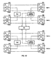
- FIGS. 1A, 1B and 1C are electrical schematic diagrams of three different variants of PoE as contemplated by the IEEE 802.3af standard.
- a data telecommunications network 10a comprises a switch or hub 12a with integral power sourcing equipment (PSE) 14a. Power from the PSE 14a is injected on the two data carrying Ethernet twisted pairs 16aa and 16ab via center-tapped transformers 18aa and 18ab. Non-data carrying Ethernet twisted pairs 16ac and load are unused in this variant. The power from data carrying Ethernet twisted pairs 16aa and 16ab is conducted from center-tapped transformers 20aa and 20ab to powered device (PD) 22a for use thereby as shown.
- PSE power sourcing equipment
- a data telecommunications network 10b comprises a switch or hub 12b with integral power sourcing equipment (PSE) 14b. Power from the PSE 14b is injected on the two non-data carrying Ethernet twisted pairs 16bc and 16bd. Data carrying Ethernet twisted pairs 16ba and 16bb are unused in this variant for power transfer. The power from non-data carrying Ethernet twisted pairs 16bc and 16bd is conducted to powered device (PD) 22b for use thereby as shown.
- PD powered device
- a data telecommunications network 10c comprises a switch or hub 12c without integral power sourcing equipment (PSE).
- Midspan power insertion equipment 24 simply passes the data signals on the two data carrying Ethernet twisted pairs 16ca-1 and 16cb-1 to corresponding data carrying Ethernet twisted pairs 16ca-2 and 16cb-2. Power from the PSE 14c located in the Midspan power insertion equipment 24 is injected on the two non- data carrying Ethernet twisted pairs 16cc-2 and 16cd-2 as shown. The power from non- data carrying Ethernet twisted pairs 16cc-2 and 16cd-2 is conducted to powered device (PD) 22c for use thereby as shown.
- powered end stations 26a, 26b and 26c are all the same so that they can achieve compatibility with each of the previously described variants.
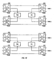
- FIGS. 1D and 1E electrical schematic diagrams illustrate variants of the IEEE 802.3af standard in which 1000 Base T communication is enabled over a four pair Ethernet cable.
- Inline Power may be supplied over two pair or four pair.
- the PD accepts power from a pair of diode bridge circuits such as full wave diode bridge rectifier type circuits well known to those of ordinary skill in the art. Power may come from either one or both of the diode bridge circuits, depending upon whether Inline Power is delivered over Pair 1-2, Pair 3-4 or Pair 1-2 + Pair 3-4.
- a PD associated with Pair 1-2 is powered by Inline Power over Pair 1-2 and a PD associated with Pair 3-4 is similarly powered. The approach used will depend upon the PD to be powered.
- bidirectional full duplex communication may be carried out over each data pair, if desired.
- Inline Power is also available through techniques that are non-IEEE 802.3 standard compliant as is well known to those of ordinary skill in the art.
- WO-A1-96/23377 describes a multimedia system having a central power source and distribution subsystem.
- the power subsystem provides phantom power and third pair power via a computer network bus.
- US-A1-2004/0049321 discloses a system for power delivery over data communication cabling infrastructure.
- the system includes power/data combiners that combine a data communication signal with a low frequency power signal.
- US-A-5,148,144 describes a data communication network for delivering power and communications over the same cable bundle.
- imbalance in the current carried by the first and second conductors of the pair of conductors is detected and compensated with a bias current applied to counter the imbalance.
- Embodiments of the present invention described in the following detailed description are directed at current imbalance compensation for magnetics in a wired data telecommunications network.
- Other embodiments of the present invention, beyond those embodiments described in the detailed description, will readily suggest themselves to those of ordinary skill in the art having the benefit of this disclosure.
- Network segment 50 comprises a first pair of conductors 52 comprised of first conductor 54 and second conductor 56 and a second pair of conductors 53.
- a center-tapped transformer T1 and T2 On either side of the pair of conductors is a center-tapped transformer T1 and T2.
- the primary winding P of transformer T1 is coupled to a PHY and the secondary winding S is coupled via a coupler such as an RJ-45 connector to the first pair of conductors (wire side).
- a direct current (DC) signal such as an inline power signal is transmitted using common mode inline power transmission some current will traverse the first conductor 54 and other current will traverse the second conductor 56.
- DC direct current
- RA and RB can be influenced in a twisted pair network connection by cable length, variations in the cable material, bends in the cable, corrosion in the connectors at either end of the network segment, mismatches in the winding resistance within a magnetic device due to wire- diameter mismatch, and the like. Accordingly, RA and RB often differ somewhat. Where the cables are relatively long, the difference is often less important than where the cables are relatively short due to the swamping effect of the larger resistance of a longer cable.
- a difference in the inline power current within the two conductors of a twisted pair can lead to a phenomenon known as droop.
- a phenomenon known as droop Where there is a substantial current imbalance between the two sides on either side of the center tap in a central- tapped magnetic device such as one of transformers T1 and T2 then saturation in the magnetic device can cause the data signals which pass through the transformers to become distorted.
- the windings on either side of the center tap are normally wound in opposite directions, so that if equal DC currents flow towards the center tap from either side, the net DC current seen by the transformer core is zero. If the currents are not equal, the transformer core sees a nonzero current, and a sufficiently large current causes degradation of the transfer characteristic of the transformer, the phenomenon known as droop. When the droop is sufficiently large the distortion can affect the data throughput on the network segment leading to data errors.
- FIGS. 4A and 4B illustrate the problem of droop.
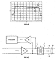
- Curve A of FIG. 4A is an illustration of a data signal pulse not impacted by droop.
- Curve B of FIG. 4A is an illustration of a distorted data pulse where the distortion is caused by a transformer subjected to a 50mA current bias on one leg which forces a current imbalance in the transformer and causes a droop of over two 200mV divisions. (Note that the curves are offset by a DC offset of about 1.5 divisions for clarity).
- Curve A is relatively well behaved and stays within a range of well less than 200 mV (one division) during its on-time, whereas Curve B is relatively badly behaved varying over about three times as much in amplitude during its on-time.
- FIG. 4B illustrates the correction of the droop by compensating for it by applying another 50mA signal (causing a countering DC current) to the other leg of the transformer. Curve A of FIG. 4B is the essentially the same as Curve A of FIG. 4A .
- droop is measured, compensation current is applied, and the droop is thereby reduced.
- the droop may be measured by coupling a receiver to the transmitter output at the PHY. This is illustrated at FIG. 4C .
- Transmitter TX transmits a differential AC signal into the primary of transformer T1.
- An effective current imbalance in current carried by conductors 54 and 56 on the wire side of transformer T1 (forming a circuit element) may cause signal droop. That droop will be present on both the primary and the secondary of transformer T1.
- Receiver RX is coupled to receive and monitor the signal transmitted by transmitter TX as shown.
- a processor determines if there is droop by comparing the (possibly) distorted pulse (or characteristics thereof) to an expected or ideal pulse (or characteristics thereof). This may be done, for example, by measuring the peak amplitude or the amplitude at some point in the pulse, for example, near the end of the pulse where the droop usually tends to be more pronounced. This amplitude is compared to the expected or desired amplitude and a difference error signal related to the magnitude of the droop is generated.
- a feedback loop which applies a correcting DC current to an appropriate node of the circuit (as discussed below) in order to counter the unbalanced current flow on the wire side of the magnetic device and thereby bring the difference error signal to zero or nearly zero and so reduce the droop and correct the shape of the pulse.
- the measurement of the droop and/or effective current imbalance may take place on either the primary side or the secondary side of the magnetic device T1 and the correcting DC current may be induced on the primary side of the magnetic as with a third winding on the primary side of magnetic device T1 or by direct current injection or induced current injection on the secondary side (wire side) of magnetic device T1.
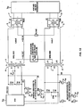
- FIG. 5 an embodiment 60 of the present invention is shown in schematic diagram form. Note that while this figure illustrates two pairs of conductors, the invention includes implementations operating on one or more pairs of conductors and is intended to include, for example, both two pair and four pair Ethernet embodiments such as 10 Base T, 100 Base T, 1000 Base T and higher.
- the embodiments of the present invention may easily be implemented at the PSE side (e.g., a network hub or switch), however, they may be implemented at either the PSE or the PD, or even in the middle of the cable run, if desired. If implemented on both sides, an auto-negotiation process to allow one side to act while the other allows it to act is necessary to avoid a situation where both sides are trying to compensate for unbalanced current at the same time (and possibly making the situation worse).
- PSE side e.g., a network hub or switch
- the PHY's IEEE 802.3 auto-negotiation process that happens ahead of any data transmission and after the far end device (e.g., a PD) has been inline-powered, allows both sides of the link to exchange extra information via the Next Page protocol of the IEEE 802.3 auto-negotiation process, or, using proprietary pulses in a similar manner. Such 'information' exchange allows both sides to agree whether one side will do the current correction, or both, or neither.
- the PHY i.e., element 62 shown in FIG. 5
- similar circuitry would be responsible for correcting an effective current imbalance on both pairs potentially using the data pulses, especially if it is determined that the inline power device is not capable of correcting current imbalance (i.e., no auto-negotiation reply is received indicating such a capability at the far end device).
- the single-sided effective current imbalance correction can take place in at least two ways: (1) the local PHY transmits on both its Transmit and Receive channels either data or a special droop detection pulse or pulses designed to be wide enough in width (time - e.g., 400 - 1000 nSec in one embodiment) to highlight the droop without appearing to be data pulses, and the effective current imbalance is measured leading to the proper correction through a conventional feedback circuit; or (2) the data pulses themselves are used for sensing the effective current imbalance allowing the local receiver to automatically cause the application of the proper correction, since it can detect both data errors and droop.
- data pulses have different frequency content and may not all be affected by droop in the same way, potentially making it harder to sense the droop on all data pulses, hence it maybe desirable at least in some circumstances to use out of band (non-data) droop detection pulses for this purposes.
- the circuitry may opt out of the correction process (this can be an appropriate choice where the cable between the two devices is long enough that any current imbalance present does not affect the data due to the swamping effect of the long cable resistance, or under certain conditions where the SNR (signal to noise ratio) is acceptable for data communications purposes.
- the two sides may negotiate to have their respective transmitter's imbalance corrected locally. This is done in the same way using the local PHY or similar circuitry by acting on transmitted data pulses or droop detection pulses, as discussed above, to correct for the imbalance.
- 10/100 devices will 'attach' the correction to the local transmitter, allowing it the flexibility of controlling the test signal and increasing the accuracy of the current sense since no cable attenuation is involved.
- the effective current imbalance correction can be either (1) continuously adaptive (i.e., it automatically corrects at any time an effective current imbalance is presented (such as due to changes in temperature, power load level, transmission speed, and the like); or (2) fixed (i.e., it corrects/calibrates once ahead of data transmission, after the PD is powered up, and possibly revisits the correction of a potential imbalance if the PSE or the PD communicates power requirement changes, if the link goes down, the cable has been unplugged, local receive errors are detected, software/firmware determines a need to re-correct, and the like).
- the correction for effective current imbalance can be active at all times, or enabled/disabled via software/firmware.
- the correction process may be set up to initiate when the PHY detects idle periods where no data transmission is taking place. During such idle periods it would initiate the sense and correct algorithm without taking the link down since it takes much more than a few 100's of nanoseconds to cause the link test to fail in these technologies (i.e., the PHY would transmit its test pulse, and switch back to the transmission of idles or whatever signals it needs to send out to indicate the presence of a link partner). Where the wire side-based sense and correct method is used, then the data may not be directly involved since the current sense circuitry automatically does the task without a need to interpret data pulse distortion.
- a device such as a PHY desiring to send (or receive) data over a pair of conductors (such as a twisted pair of conductors) typically does so through a transformer using differential signaling.
- a transformer using differential signaling This is illustrated in detail in the various embodiments discussed in conjunction with FIG. 1A - FIG. 1E .
- the transformers may be center-tapped transformers or a pair of inductors with a center node emulating a center-tapped transformer, hi any event, in accordance with the embodiment of FIG.
- the invention adds a third winding in addition to the primary and secondary windings of the transformer(s) and, in response to detected current imbalances, current sources and/or sinks coupled to such third windings induce current flow in the pair of conductors 76 which counters the imbalance and acts to reduce or eliminate signal droop due to transformer saturation and the like.
- PHY 62 has a transmit differential pair of conductors 64 and a receive differential pair of conductors 66.
- a first transformer or magnetic device 68 includes a PHY-side primary winding 70 which is usually center-tapped so that the center tap node may be biased to a fixed voltage such as ground.
- secondary winding 72 On the wire side of the magnetic device 68 is secondary winding 72 which is center-tapped so that inline PSE power circuitry 74 may couple common mode DC power to the differential pairs of conductors 76 and 78 via center taps 80 and 82, respectively, of magnetic device 68 secondary winding 72 and magnetic device 84 secondary winding 86.
- Current imbalance in pair 76 is detected in this embodiment by PHY-based monitoring of the outgoing pulses.
- the current sources and sinks used may be simple transistors or pairs of transistors such as MOSFETs configured as sources/sinks as well known to those of ordinary skill in the art and that they should appear as high impedance, i.e., " 1000 ohms up to 100 MHz and they supply only DC current needed to adjust the imbalance on the wire side.
- FIG. 7 another embodiment of the present invention is presented.
- current adjustment operates much like the embodiments of FIG. 5 or FIG. 6 , however, current imbalance is sensed directly on the secondary (wire) side rather than indirectly on the primary side by inspection of pulse distortion effects.
- the secondary winding is split as shown and each leg has a current sensor in it, here shown as a current sense resistor Rsense.
- the resistance of Rsense may be much less than the 3.3 ohms of the ballast resistor R shown in FIG. 3 , e.g., about 1 ohm in one embodiment of the present invention, so this arrangement washes less power than that of the prior art.
- the terminals of the current sensor are coupled (not shown) to a voltage monitoring circuit (which may be included in block 108) to sense the voltage drop across the sense resistor. This is indicative of current.
- a voltage monitoring circuit which may be included in block 108 to sense the voltage drop across the sense resistor. This is indicative of current.
- Other techniques for current measurement may alternatively be employed such as Hall Effect sensors, and the like, as will now be appreciated by those of ordinary skill in the art.
- An adjust signal on one or more lines 110 is generated at block 108 to control the current sinks and sources associated with the current compensation circuitry on the primary side of the magnetic devices. When the block 108 determines that current is balanced, it may hold the setting for the adjust signal until requested to adjust the balance again as discussed above.
- FIG. 8 a version of the embodiment of FIG. 7 is presented using the simplified current sink/source approach first illustrated in FIG 6 . Note that third windings 111a and 111b are coupled in series with respective primary windings 70a and 70b.
- FIG. 9 another embodiment of the present invention is presented.
- current compensation is provided by third windings 112, 114 on the wire side (secondary side) of the magnetic devices 68b, 84b.
- Current is sensed directly on the wire side as in FIGS. 7 and 8 , however the current sink/source arrangement provides current to third windings 112, 114 on the secondary (wire) side rather than a third winding on the primary side as in FIGS. 5 , 6 , 7 and 8 .
- FIG. 10 another embodiment of the present invention is illustrated.
- a third winding in a differential transformer is not provided, rather, current imbalance is sensed as in FIGS. 7 , 8 and 9 and compensating current is directly applied to the conductor pairs isolating the current sources/sinks from the conductor pairs with an appropriate inductor (e.g., 1mH) as shown.
- an appropriate inductor e.g. 1mH
- FIG. 11 illustrates another embodiment of the present invention wherein compensating current is directly applied to the primary of T1 instead of via a third winding, hi this case a current source/sink is coupled to one or both ends of the primary as shown through an inductance. While two sets of current source/sinks are shown in this version, those of ordinary skill in the art will now appreciate that a number of different configurations could be employed. More specifically, the center tap of the primary of T 1 is shown strapped to Vdd (typically 3.3 VDC in most PHYs) although it can instead be set to any convenient fixed voltage such as ground. The PHY steers DC current in and out of L1 and L2 (which are parts of the primary winding of magnetic device T1) during data transmission.
- Vdd typically 3.3 VDC in most PHYs
- Inductors L13 and L14 provide high AC impedance and low DC impedance so that current sources/sinks may be used to push DC current though L1 or L2 from a current source referenced to a higher supply, 5VDC shown here, or pull current from L1 and L2 to ground (or a lower supply) via the L13 and L14 windings.
- current source 13 may be used to sink current to ground though the L14 inductor, that is flowing really though L2 that is biased to 3.3v at the center tap
- OR current source 16 may be used to force current from the 5v supply through L14 inductor and into L2 sinking the current into the 3.3v supply at the center tap of the primary of T 1.
- Other approaches may also be used and combinations may be used as well, if desired.
- L1 3. Note that current adjustment will typically occur at L13 OR L14 but not both. Similarly, current may be sinked into the 3.3 VDC supply or 0VDC supply, but not both.
- the current sources/sinks are used subject to the constraint that one uses either one side (L1 or L2) of the T1 primary winding to pull current in or out, but not both; or one may use either one side (e.g., L13) or the other (e.g., L14) but not both sides source/sink current to/from the primary winding of T1.
- the embodiment illustrated in the schematic diagram of FIG. 12 is a slight variation on the embodiment of FIG. 11 . In this version the two 50-ohm termination resistors R3 and R4 on the transmit side and R1 and R2 on the receive side are shown (although they would be present in all embodiments that operate with Ethernet).
- the current sources do the adjustment right across the typical Ethernet link on the primary side, the sources must look like a relatively high impedance (e.g., more than 1000 ohms) up to 100mhz and must be designed with low capacitance (i.e., no more than a few picofarads), and must keep the signal balanced since there is no isolation in this embodiment for the TX or the RX pairs.
- a current source in inside the PHY steers AC data current at higher speeds. Effectively another DC current source is added so that it is ON when needed and only applies DC current as an offset.
- the current sources are much higher impedance than the 100 ohm by at least a ratio of 10 to 1 and are low capacitance.
- FIG. 13 The embodiment illustrated in the schematic diagram of FIG. 13 is a slight variation on the embodiment of FIG. 12 .
- inductors L13 and L14 are added back (as from FIG. 11 ) on the transmit channel, and the same concepts as discussed with respect to FIG. 12 apply except that the transmit channel AC (data) signals are isolated with inductors L 13/L 14 giving the PHY designer the chance to design a current source that may be more capacitive and potentially correcting for a higher offset or error, i.e., one providing much higher DC current correction.
- the receive channel while it could be configured like the transmit channel, in this version the center- tap is split on the primary side as shown which avoids the need for a dedicated winding to do the job.
- Capacitors C2 and C3 to ground eliminate common mode noise, and the current adjustment takes place as discussed above.
- TDR time domain reflectometers
- FIG. 14 illustrates a variation 140 of the approach shown in FIG. 4C and utilizes a digital signal processor (DSP) 142 or equivalent circuitry on the transmit portion 144 of the PHY 146.
- the transmitter (transmit DAC (current-output digital analog converter)) 148 transmits a differential analog signal on lines 150a, 150b to the primary 152 of transmit transformer T1 154.
- Receiver 156 is coupled to receive the output of transmitter 148 on lines 150a, 150b via lines 158a, 158b.
- Receiver 156 outputs a digital version of the signal from transmitter 148 to an input 160 of DSP 142.
- the digital output on line 162 of DSP 142 constitutes a feedback signal. Test pulses can be initiated, for example, in transmitter 148.
- the receiver 156 senses this and in conjunction with DSP 142 causes a correction to the signal so that after a few pulses have been sent and sensed, the transmit portion 144 of the PHY 146 is able to send a predistorted signal that looks perfect or near perfect upon passing through transformer T1 (154).
- FIG. 15 is an electrical schematic diagram which illustrates an example of a circuit for providing current sink/current source capability for the circuits described in more detail above. This is just one example and many other equivalent circuits may be used which are capable of sinking or sourcing current.
- a controller 120 is coupled to a current imbalance detector 122 which may be of a type adapted for direct measurement of current imbalance (wire side current sensors) or indirect measurement of effective current imbalance (droop detection) as described in more detail above.
- Controller 120 is coupled to a pair of voltage DACs (digital to analog converters with voltage outputs) 124 and 126. These pass a signal to conventional current sink circuit block 128 and current source circuit block 130, respectively, which are arranged to drive a bias current in either direction.
- node CTAP may alternatively be grounded or set to some other fixed voltage level.
- a current sink/source circuit may be located in various places in the circuit to achieve the corrective action described herein and various types of sensing may be used to cause it to act.
Abstract
Description
- This patent may be considered to be related to commonly owned United States Patent Publication No.
US 2006 088 230 A1 published on April 27, 2006 and entitled "Bidirectional Inline Power Port" in the names of inventors Daniel Biederman, Kenneth Coley and Frederick R. Schindler. - This patent may also be considered to be related to commonly owned United States Patent Publication. No.
US 2006 080 573 A1 published on April 13, 2006 and entitled "Redundant Power and Data Over A Wired Data Telecommunications Network" in the names of inventors Daniel Biederman, Kenneth Coley and Frederick R. Schindler . - This patent may also be considered to be related to commonly owned United States Patent Publication. No.
US 2006 082 220 A1 published on April 20, 2006 and entitled "Inline Power - Based Common Mode Communications in a Wired Data Telecommunications Network" in the names of inventors Roger A. Karam, Frederick R. Schindler and Wael William Diab - This patent may also be considered to be related to commonly owned United States Patent Publication No.
US 2006 092 826 A1 published on May 4, 2006 and entitled "Automatic System for Power and Data Redundancy in a Wired Data Telecommunications Network" in the names of inventors Roger A. Karam and Luca Cafiero . - This patent may also be considered to be related to commonly owned United States Patent Publication. No.
US 2006 100799 A1 published on May 11, 2006 and entitled "Power Management for Serial-Powered Device Connections" in the name of inventor Roger A. Karam . - This patent may also be considered to be related to commonly owned United States Patent Publication. No.
US2006 077888 A1 published on April 13, 2006 and entitled "Redundant Power and Data In A Wired Data Telecommunications Network" in the names of inventors Roger A. Karam and Luca Cafiero. - This patent may also be considered to be related to commonly owned United States Patent Publication. No.
US 2006 078 093 A1 published on April 13, 2006 and entitled "Power and Data Redundancy in a Single Wiring Closet" in the names of inventors Roger A. Karam and Luca Cafiero. - This patent may also be considered to be related to commonly owned United States Patent Publication. No.
US 2006 092 000 A1 published on May 4, 2006 and entitled Powered Device Classification In A Wired Data Telecommunications Network" in the name of inventors Roger A. Karam and John F. Wakerly. - This patent may also be considered to be related to commonly owned United States Patent Publication No.
US 2008 244 284 A1 published on October 2, 2008 and entitled "Improved Power Delivery over Ethernet Cable" in the names of inventors Wael William Diab and Frederick R. Schindler. - This patent may also be considered to be related to commonly owned United States Patent Publication No.
6,541,878 published on April 1, 2003 and entitled "Integrated RJ-45 Magnetics with Phantom Power Provision" in the name of inventor Wael William Diab. - This patent may also be considered to be related to commonly owned United States Patent Publication No.
US 2005 262364 A1 published on November 24, 2005 and entitled "Methods and Apparatus for Provisioning Phantom Power to Remote Devices" in the name of inventors Wael William Diab and Frederick R. Schindler. - This patent may also be considered to be related to co-pending commonly owned United States Patent Publication No.
US 6958699 B1 published on October 25, 2005 and entitled "Signal Disruption Detection in Powered Networking Systems" in the name of inventor Roger A. Karam. - The present invention relates generally to networking equipment which is powered by and/or powers other networking equipment over wired data telecommunications network connections.
- Inline Power (also known as Power over Ethernet and PoE) is a technology for providing electrical power over a wired data telecommunications network (such as, for example, the well-known Ethernet) from power source equipment (PSE) to a powered device (PD) over a link section. The power may be injected by an endpoint PSE at one end of the link section or by a midspan PSE along a midspan of a link section that is distinctly separate from and between the media dependent interfaces (MDIs) to which the ends of the link section are electrically and physically coupled.
- PoE is defined in the IEEE (The Institute of Electrical and Electronics Engineers, Inc.) Standard Std 802.3af-2003 published 18 June 2003 and entitled "IEEE Standard for Information technology - Telecommunications and information exchange between systems - Local and metropolitan area networks - Specific requirements:
Part 3 Carrier Sense Multiple Access with Collision Detection (CSMA/CD) Access Method and Physical Layer Specifications: Amendment: Data Terminal Equipment (DTE) Power via Media Dependent Interface (MDI)" (herein referred to as the "IEEE 802.3af standard"). The IEEE 802.3af standard is a globally applicable standard for combining the transmission and reception (collectively: "transceiving") of Ethernet packets with the transmission and reception of DC-based power over the same set of wires in a single Ethernet cable. It is contemplated that Inline Power will power such PDs as Internet Protocol (IP) telephones, surveillance cameras, switching and hub equipment for the telecommunications network, biomedical sensor equipment used for identification purposes, other biomedical equipment, radio frequency identification (RFID) card and tag readers, security card readers, various types of sensors and data acquisition equipment, fire and life-safety equipment in buildings, and the like. The power is direct current, floating 48 Volt power currently available at a range of power levels from about 4 watts to about 15 watts in accordance with the standard. There are mechanisms within the IEEE 802.3af standard to allocate a requested amount of power. Other proprietary schemes also exist to provide a finer and more sophisticated allocation of power than that provided by the IEEE 802.3af standard while still providing basic compliance with the standard. As the standard evolves, additional power may also become available. Conventional 8-conductor type RG-45 connectors (male or female, as appropriate) are typically used on both ends of all Ethernet connections. They are wired as defined in the IEEE 802.3af standard. -
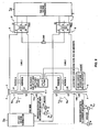
FIGS. 1A, 1B and 1C are electrical schematic diagrams of three different variants of PoE as contemplated by the IEEE 802.3af standard. InFIG. 1A adata telecommunications network 10a comprises a switch orhub 12a with integral power sourcing equipment (PSE) 14a. Power from the PSE 14a is injected on the two data carrying Ethernet twisted pairs 16aa and 16ab via center-tapped transformers 18aa and 18ab. Non-data carrying Ethernet twisted pairs 16ac and load are unused in this variant. The power from data carrying Ethernet twisted pairs 16aa and 16ab is conducted from center-tapped transformers 20aa and 20ab to powered device (PD) 22a for use thereby as shown. InFIG. 1B adata telecommunications network 10b comprises a switch orhub 12b with integral power sourcing equipment (PSE) 14b. Power from thePSE 14b is injected on the two non-data carrying Ethernet twisted pairs 16bc and 16bd. Data carrying Ethernet twisted pairs 16ba and 16bb are unused in this variant for power transfer. The power from non-data carrying Ethernet twisted pairs 16bc and 16bd is conducted to powered device (PD) 22b for use thereby as shown. InFIG. 1C adata telecommunications network 10c comprises a switch orhub 12c without integral power sourcing equipment (PSE). Midspanpower insertion equipment 24 simply passes the data signals on the two data carrying Ethernet twisted pairs 16ca-1 and 16cb-1 to corresponding data carrying Ethernet twisted pairs 16ca-2 and 16cb-2. Power from thePSE 14c located in the Midspanpower insertion equipment 24 is injected on the two non- data carrying Ethernet twisted pairs 16cc-2 and 16cd-2 as shown. The power from non- data carrying Ethernet twisted pairs 16cc-2 and 16cd-2 is conducted to powered device (PD) 22c for use thereby as shown. Note that poweredend stations - Turning now to
FIGS. 1D and1E , electrical schematic diagrams illustrate variants of the IEEE 802.3af standard in which 1000 Base T communication is enabled over a four pair Ethernet cable. Inline Power may be supplied over two pair or four pair. InFIG. 1D the PD accepts power from a pair of diode bridge circuits such as full wave diode bridge rectifier type circuits well known to those of ordinary skill in the art. Power may come from either one or both of the diode bridge circuits, depending upon whether Inline Power is delivered over Pair 1-2, Pair 3-4 or Pair 1-2 + Pair 3-4. In the circuit shown inFIG. 1E a PD associated with Pair 1-2 is powered by Inline Power over Pair 1-2 and a PD associated with Pair 3-4 is similarly powered. The approach used will depend upon the PD to be powered. In accordance with both of these versions, bidirectional full duplex communication may be carried out over each data pair, if desired. - Inline Power is also available through techniques that are non-IEEE 802.3 standard compliant as is well known to those of ordinary skill in the art.
- In many cases where PDs are used, it may be desirable to provide some redundancy in terms of data and/or power delivery for cases in which equipment (hubs, switches, cable and the like) providing the power and/or data fails to continue to do so.
-
WO-A1-96/23377 -
US-A1-2004/0049321 discloses a system for power delivery over data communication cabling infrastructure. The system includes power/data combiners that combine a data communication signal with a low frequency power signal. -
US-A-5,148,144 describes a data communication network for delivering power and communications over the same cable bundle. - Aspects of the invention are set out in the independent claims and preferred features are set out in the dependent claims.
- In a circuit delivering common mode inline power over a pair of conductors, imbalance in the current carried by the first and second conductors of the pair of conductors is detected and compensated with a bias current applied to counter the imbalance.
- Other embodiments are described below, and a further understanding of the nature and advantages of the inventions may be realized by reference to the remaining portions of the specification and the attached drawings.
- The accompanying drawings, which are incorporated into and constitute a part of this specification, illustrate one or more embodiments of the present invention and, together with the detailed description, serve to explain the principles and implementations of the invention. In the drawings:
-
FIGS. 1A, 1B, 1C ,1D and1E are electrical schematic diagrams of portions of data telecommunications networks in accordance with the prior art. -
FIG. 2 is an electrical schematic diagram of a segment of a wired data telecommunications network comprising two pairs of conductors adapted for transmission of inline power. -
FIG. 3 is an electrical schematic diagram of a current compensation technique in accordance with the prior art. -
FIGS. 4A and4B are graphs illustrating the effects of inline power current imbalance and imbalance compensation on data transmitted over the inline power conductors. -
FIG. 4C is an electrical schematic diagram of a portion of a transmitter section of an apparatus in accordance with an embodiment of the present invention. -
FIGS. 5 ,6 ,7 ,8 ,9 ,10 ,11 ,12 and13 are electrical schematic diagrams of various current compensation schemes in accordance with embodiments of the present invention. -
FIG. 14 is an electrical schematic diagram of a portion of a transmitter section of an apparatus in accordance with an embodiment of the present invention. -
FIG. 15 is an electrical schematic diagram of a current imbalance detection and injection circuit in accordance with an embodiment of the present invention. - Embodiments of the present invention described in the following detailed description are directed at current imbalance compensation for magnetics in a wired data telecommunications network. Other embodiments of the present invention, beyond those embodiments described in the detailed description, will readily suggest themselves to those of ordinary skill in the art having the benefit of this disclosure. Reference will now be made in detail to implementations of the present invention as illustrated in the accompanying drawings. Where appropriate, the same reference indicators will be used throughout the drawings and the following detailed description to refer to the same or similar parts.
- In the interest of clarity, not all of the routine features of the implementations described herein are shown and described. It will, of course, be appreciated that in the development of any such actual implementation, numerous implementation-specific decisions must be made in order to achieve the developer's specific goals, such as compliance with application- and business-related constraints, and that these specific goals will vary from one implementation to another and from one developer to another. Moreover, it will be appreciated that such a development effort might be complex and time-consuming, but would nevertheless be a routine undertaking of engineering for those of ordinary skill in the art having the benefit of this disclosure.
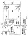
- Turning now to
FIG. 2 anetwork segment 50 is illustrated.Network segment 50 comprises a first pair ofconductors 52 comprised offirst conductor 54 andsecond conductor 56 and a second pair ofconductors 53. On either side of the pair of conductors is a center-tapped transformer T1 and T2. The primary winding P of transformer T1 is coupled to a PHY and the secondary winding S is coupled via a coupler such as an RJ-45 connector to the first pair of conductors (wire side). When a direct current (DC) signal such as an inline power signal is transmitted using common mode inline power transmission some current will traverse thefirst conductor 54 and other current will traverse thesecond conductor 56. Ideally that current would be the same, however Ohm's law dictates that any difference in the resistance between the two legs of the pair ofconductors 52 will force more current into one than travels through the other. Here the resistance in the two legs is illustrated by the resistors RA and RB. RA and RB can be influenced in a twisted pair network connection by cable length, variations in the cable material, bends in the cable, corrosion in the connectors at either end of the network segment, mismatches in the winding resistance within a magnetic device due to wire- diameter mismatch, and the like. Accordingly, RA and RB often differ somewhat. Where the cables are relatively long, the difference is often less important than where the cables are relatively short due to the swamping effect of the larger resistance of a longer cable. - A difference in the inline power current within the two conductors of a twisted pair can lead to a phenomenon known as droop. Where there is a substantial current imbalance between the two sides on either side of the center tap in a central- tapped magnetic device such as one of transformers T1 and T2 then saturation in the magnetic device can cause the data signals which pass through the transformers to become distorted. The windings on either side of the center tap are normally wound in opposite directions, so that if equal DC currents flow towards the center tap from either side, the net DC current seen by the transformer core is zero. If the currents are not equal, the transformer core sees a nonzero current, and a sufficiently large current causes degradation of the transfer characteristic of the transformer, the phenomenon known as droop. When the droop is sufficiently large the distortion can affect the data throughput on the network segment leading to data errors.
- Even if currents are equal, droop may occur due to imprecision in the manufacture of the transformer, e.g., if the number of turns on either side of the center tap is not precisely the same. Thus, an effective current imbalance and corresponding droop may be due to an actual current imbalance or may be due to imprecision in the manufacture of the transformer, or both. Some of the apparatus and methods described in this disclosure detect droop and therefore can compensate for an effective current imbalance regardless of its cause. Others rely on a measurement of actual current imbalance and will not compensate for imprecision in transformer center tap positioning.
- For relatively small inline power currents there will be correspondingly small amounts of droop and the problem will usually be insignificant. For example, the IEEE 802.3af standard at Annex 33E suggests that-current balance can be achieved by using the ballast arrangement illustrated in
FIG. 3 . Power dissipation in resistors, however, is given by P=I2R. The parallel 3.3 ohm resistances proposed by the standard will dissipate about 0.2 watt per powered pair while such a circuit delivers 350 mA (roughly 40 watts of waste heat dissipation for a 48 port device with all four pairs carrying power). However, as inline power technology is adapted to provide larger and larger currents, this problem increases with the square of the current. Thus at 1000 mA of current per pair, the same device would have to dissipate over 300 watts. Accordingly, for larger inline power levels, the ballast-type approach suggested in the IEEE 802.3af standard will soon become impractical due to the unacceptably high levels of waste heat (and wasted electrical power). -
FIGS. 4A and4B illustrate the problem of droop. Curve A ofFIG. 4A is an illustration of a data signal pulse not impacted by droop. Curve B ofFIG. 4A is an illustration of a distorted data pulse where the distortion is caused by a transformer subjected to a 50mA current bias on one leg which forces a current imbalance in the transformer and causes a droop of over two 200mV divisions. (Note that the curves are offset by a DC offset of about 1.5 divisions for clarity). As can be seen by inspection, Curve A is relatively well behaved and stays within a range of well less than 200 mV (one division) during its on-time, whereas Curve B is relatively badly behaved varying over about three times as much in amplitude during its on-time.FIG. 4B illustrates the correction of the droop by compensating for it by applying another 50mA signal (causing a countering DC current) to the other leg of the transformer. Curve A ofFIG. 4B is the essentially the same as Curve A ofFIG. 4A . - Detection of droop is described, for example, in co-pending and commonly owned
U.S. Patent Application Serial No. 10/033,808 filed December 18, 2001 and entitled "Signal Disruption Detection in Powered Networking Systems" in the name of inventor Roger A. Karam. - In accordance with one embodiment of the present invention, droop is measured, compensation current is applied, and the droop is thereby reduced. The droop may be measured by coupling a receiver to the transmitter output at the PHY. This is illustrated at
FIG. 4C . Transmitter TX transmits a differential AC signal into the primary of transformer T1. An effective current imbalance in current carried byconductors - Turning now to
FIG. 5 , anembodiment 60 of the present invention is shown in schematic diagram form. Note that while this figure illustrates two pairs of conductors, the invention includes implementations operating on one or more pairs of conductors and is intended to include, for example, both two pair and four pair Ethernet embodiments such as 10 Base T, 100 Base T, 1000 Base T and higher. The embodiments of the present invention may easily be implemented at the PSE side (e.g., a network hub or switch), however, they may be implemented at either the PSE or the PD, or even in the middle of the cable run, if desired. If implemented on both sides, an auto-negotiation process to allow one side to act while the other allows it to act is necessary to avoid a situation where both sides are trying to compensate for unbalanced current at the same time (and possibly making the situation worse). - In the case of 10 Base T and 100 Base T Ethernet, data transmission takes place over two pairs in the cable. In accordance with one embodiment of the present invention where PHY-based detection and correction takes place, the PHY's IEEE 802.3 auto-negotiation process that happens ahead of any data transmission and after the far end device (e.g., a PD) has been inline-powered, allows both sides of the link to exchange extra information via the Next Page protocol of the IEEE 802.3 auto-negotiation process, or, using proprietary pulses in a similar manner. Such 'information' exchange allows both sides to agree whether one side will do the current correction, or both, or neither. If the agreement is reached to do the sense for droop and the current imbalance correction on one side of the link, the PHY (i.e.,
element 62 shown inFIG. 5 ) or similar circuitry would be responsible for correcting an effective current imbalance on both pairs potentially using the data pulses, especially if it is determined that the inline power device is not capable of correcting current imbalance (i.e., no auto-negotiation reply is received indicating such a capability at the far end device). The single-sided effective current imbalance correction can take place in at least two ways: (1) the local PHY transmits on both its Transmit and Receive channels either data or a special droop detection pulse or pulses designed to be wide enough in width (time - e.g., 400 - 1000 nSec in one embodiment) to highlight the droop without appearing to be data pulses, and the effective current imbalance is measured leading to the proper correction through a conventional feedback circuit; or (2) the data pulses themselves are used for sensing the effective current imbalance allowing the local receiver to automatically cause the application of the proper correction, since it can detect both data errors and droop. Note that data pulses have different frequency content and may not all be affected by droop in the same way, potentially making it harder to sense the droop on all data pulses, hence it maybe desirable at least in some circumstances to use out of band (non-data) droop detection pulses for this purposes. Also, if the local receiver does not sense any errors, the circuitry may opt out of the correction process (this can be an appropriate choice where the cable between the two devices is long enough that any current imbalance present does not affect the data due to the swamping effect of the long cable resistance, or under certain conditions where the SNR (signal to noise ratio) is acceptable for data communications purposes. - In accordance with another embodiment of the present invention, the two sides may negotiate to have their respective transmitter's imbalance corrected locally. This is done in the same way using the local PHY or similar circuitry by acting on transmitted data pulses or droop detection pulses, as discussed above, to correct for the imbalance. By sharing the correction process among them, 10/100 devices will 'attach' the correction to the local transmitter, allowing it the flexibility of controlling the test signal and increasing the accuracy of the current sense since no cable attenuation is involved.
- In the case of 1000 Base T Ethernet or other technologies that use 4-pair transmission, the same methods mentioned for 10/100's negotiation of which device will do the correction apply. The difference here is that current imbalances on two extra pairs need to be corrected. In this case one side may handle one of the pairs dedicated for 10/100, while the link partner handles the second pair, or a single side may be responsible for the full 4-pair correction.
- In general, the effective current imbalance correction can be either (1) continuously adaptive (i.e., it automatically corrects at any time an effective current imbalance is presented (such as due to changes in temperature, power load level, transmission speed, and the like); or (2) fixed (i.e., it corrects/calibrates once ahead of data transmission, after the PD is powered up, and possibly revisits the correction of a potential imbalance if the PSE or the PD communicates power requirement changes, if the link goes down, the cable has been unplugged, local receive errors are detected, software/firmware determines a need to re-correct, and the like). The correction for effective current imbalance can be active at all times, or enabled/disabled via software/firmware.
- Alternatively, the correction process may be set up to initiate when the PHY detects idle periods where no data transmission is taking place. During such idle periods it would initiate the sense and correct algorithm without taking the link down since it takes much more than a few 100's of nanoseconds to cause the link test to fail in these technologies (i.e., the PHY would transmit its test pulse, and switch back to the transmission of idles or whatever signals it needs to send out to indicate the presence of a link partner). Where the wire side-based sense and correct method is used, then the data may not be directly involved since the current sense circuitry automatically does the task without a need to interpret data pulse distortion.
- A device such as a PHY desiring to send (or receive) data over a pair of conductors (such as a twisted pair of conductors) typically does so through a transformer using differential signaling. This is illustrated in detail in the various embodiments discussed in conjunction with
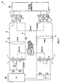
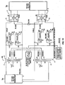
FIG. 1A - FIG. 1E . Where common mode inline power delivery is provided, the transformers may be center-tapped transformers or a pair of inductors with a center node emulating a center-tapped transformer, hi any event, in accordance with the embodiment ofFIG. 5 , the invention adds a third winding in addition to the primary and secondary windings of the transformer(s) and, in response to detected current imbalances, current sources and/or sinks coupled to such third windings induce current flow in the pair ofconductors 76 which counters the imbalance and acts to reduce or eliminate signal droop due to transformer saturation and the like. - In
FIG. 5 ,PHY 62 has a transmit differential pair ofconductors 64 and a receive differential pair ofconductors 66. A first transformer ormagnetic device 68 includes a PHY-side primary winding 70 which is usually center-tapped so that the center tap node may be biased to a fixed voltage such as ground. On the wire side of themagnetic device 68 is secondary winding 72 which is center-tapped so that inlinePSE power circuitry 74 may couple common mode DC power to the differential pairs ofconductors magnetic device 68 secondary winding 72 andmagnetic device 84 secondary winding 86. Current imbalance inpair 76 is detected in this embodiment by PHY-based monitoring of the outgoing pulses. Current imbalance inpair 78 is detected by observing droop in the signals received atPHY 62. Current correction is applied viathird windings magnetic devices FIG. 5 are a first current sink 92 and a firstcurrent source 94 both connected to a third winding on the primary side ofmagnetic device 68 with acenter tap node 96 held at a fixed voltage. Similarly, the other end of winding 88 has acurrent sink 98 and acurrent source 100. These current sources and sinks may be arranged to deliver precisely the correct amount of current in the correct direction to compensate for the current effective imbalance inconductor pair 76. A similar arrangement is provided at third winding 90 as shown. This need not be so elaborate and inFIG. 6 a similar approach uses a singlecurrent source 102 and acurrent sink 104 coupled in series with a third winding 106 oftransformer 68a. - Note that the current sources and sinks used may be simple transistors or pairs of transistors such as MOSFETs configured as sources/sinks as well known to those of ordinary skill in the art and that they should appear as high impedance, i.e., " 1000 ohms up to 100 MHz and they supply only DC current needed to adjust the imbalance on the wire side.
- Turning now to
FIG. 7 , another embodiment of the present invention is presented. In accordance with this embodiment, current adjustment operates much like the embodiments ofFIG. 5 orFIG. 6 , however, current imbalance is sensed directly on the secondary (wire) side rather than indirectly on the primary side by inspection of pulse distortion effects. Instead of using a center-tapped secondary winding atmagnetic device 68, the secondary winding is split as shown and each leg has a current sensor in it, here shown as a current sense resistor Rsense. Note that the resistance of Rsense may be much less than the 3.3 ohms of the ballast resistor R shown inFIG. 3 , e.g., about 1 ohm in one embodiment of the present invention, so this arrangement washes less power than that of the prior art. The terminals of the current sensor are coupled (not shown) to a voltage monitoring circuit (which may be included in block 108) to sense the voltage drop across the sense resistor. This is indicative of current. Other techniques for current measurement may alternatively be employed such as Hall Effect sensors, and the like, as will now be appreciated by those of ordinary skill in the art. An adjust signal on one ormore lines 110 is generated atblock 108 to control the current sinks and sources associated with the current compensation circuitry on the primary side of the magnetic devices. When theblock 108 determines that current is balanced, it may hold the setting for the adjust signal until requested to adjust the balance again as discussed above. - Turning now to
FIG. 8 , a version of the embodiment ofFIG. 7 is presented using the simplified current sink/source approach first illustrated inFIG 6 . Note thatthird windings primary windings - Turning now to
FIG. 9 , another embodiment of the present invention is presented. In accordance with this embodiment, current compensation is provided bythird windings magnetic devices FIGS. 7 and8 , however the current sink/source arrangement provides current tothird windings FIGS. 5 ,6 ,7 and8 . - Turning now to
FIG. 10 , another embodiment of the present invention is illustrated. In accordance with this embodiment, a third winding in a differential transformer is not provided, rather, current imbalance is sensed as inFIGS. 7 ,8 and9 and compensating current is directly applied to the conductor pairs isolating the current sources/sinks from the conductor pairs with an appropriate inductor (e.g., 1mH) as shown. - Note that not all of the current sources and sinks shown in
FIG. 10 must be used to effectively cancel a current imbalance. As will be understood by those skilled in the art, there are four ways to do it using only two current sources/sinks: (1) a current source and a current sink attached to the "top" conductor of the pair; (2) a current source and a current sink attached to the "bottom" conductor of the pair; (3) a current source attached to each conductor of the pair; and (4) a current sink attached to each conductor of the pair. -
FIG. 11 illustrates another embodiment of the present invention wherein compensating current is directly applied to the primary of T1 instead of via a third winding, hi this case a current source/sink is coupled to one or both ends of the primary as shown through an inductance. While two sets of current source/sinks are shown in this version, those of ordinary skill in the art will now appreciate that a number of different configurations could be employed. More specifically, the center tap of the primary ofT 1 is shown strapped to Vdd (typically 3.3 VDC in most PHYs) although it can instead be set to any convenient fixed voltage such as ground. The PHY steers DC current in and out of L1 and L2 (which are parts of the primary winding of magnetic device T1) during data transmission. Inductors L13 and L14 provide high AC impedance and low DC impedance so that current sources/sinks may be used to push DC current though L1 or L2 from a current source referenced to a higher supply, 5VDC shown here, or pull current from L1 and L2 to ground (or a lower supply) via the L13 and L14 windings. Note that even though all the possible ways of delivering current in and out of L1 and L2 to cancel the effective current imbalance in the secondary (wire) side conductor pair and rebalance the magnetic, usually only one of these options will be exercised at a time, e.g.,current source 13 may be used to sink current to ground though the L14 inductor, that is flowing really though L2 that is biased to 3.3v at the center tap, OR current source 16 may be used to force current from the 5v supply through L14 inductor and into L2 sinking the current into the 3.3v supply at the center tap of the primary ofT 1. Other approaches may also be used and combinations may be used as well, if desired. The same details apply toL1 3. Note that current adjustment will typically occur at L13 OR L14 but not both. Similarly, current may be sinked into the 3.3 VDC supply or 0VDC supply, but not both. - The same details apply to the receive winding that usually has its primary center-tap connected to ground as shown. Note that it is feasible to sink current from L1 4 (path would be 3.3VDC supply into L2 into L14 via the 13 current source to ground while at the same time the effort could be assisted by forcing current into L1 via
L1 3 into the 3.3 VDC supply originating fromcurrent source 19 and the 5VDC supply). Such active adjustment may be used if desired but one would not want to pull current fromL1 4 while trying to force current throughL 14. Also one would not want to pull current out of both L1 and L2 at the same time to ground throughL 14 and L13 for the purposes of canceling the error. Thus the current sources/sinks are used subject to the constraint that one uses either one side (L1 or L2) of the T1 primary winding to pull current in or out, but not both; or one may use either one side (e.g., L13) or the other (e.g., L14) but not both sides source/sink current to/from the primary winding of T1. [0048] The embodiment illustrated in the schematic diagram ofFIG. 12 is a slight variation on the embodiment ofFIG. 11 . In this version the two 50-ohm termination resistors R3 and R4 on the transmit side and R1 and R2 on the receive side are shown (although they would be present in all embodiments that operate with Ethernet). Note that for the purpose of the trim or adjustment we use DC current to adjust the current that usually flows through the much lower DC resistance of the windings. Here the current sources do the adjustment right across the typical Ethernet link on the primary side, the sources must look like a relatively high impedance (e.g., more than 1000 ohms) up to 100mhz and must be designed with low capacitance (i.e., no more than a few picofarads), and must keep the signal balanced since there is no isolation in this embodiment for the TX or the RX pairs. For the transmitter, usually a current source in inside the PHY steers AC data current at higher speeds. Effectively another DC current source is added so that it is ON when needed and only applies DC current as an offset. For the RX channel, since it is high impedance, past the 50 ohm terminations and into the PHY, again the current sources are much higher impedance than the 100 ohm by at least a ratio of 10 to 1 and are low capacitance. - Note that there may be a preference as to which configuration to use for tradeoff of cost, space and robustness based on which technology we are trying to work with, e.g., 10/100 or 1000 Base T; also at lower speeds one may opt to have no current compensation adjustment at all and/or such adjustments may be performed only in response to a detected Bit Error Rate increase.
- The embodiment illustrated in the schematic diagram of
FIG. 13 is a slight variation on the embodiment ofFIG. 12 . In theFIG. 13 embodiment inductors L13 and L14 are added back (as fromFIG. 11 ) on the transmit channel, and the same concepts as discussed with respect toFIG. 12 apply except that the transmit channel AC (data) signals are isolated withinductors L 13/L 14 giving the PHY designer the chance to design a current source that may be more capacitive and potentially correcting for a higher offset or error, i.e., one providing much higher DC current correction. As for the receive channel, while it could be configured like the transmit channel, in this version the center- tap is split on the primary side as shown which avoids the need for a dedicated winding to do the job. Capacitors C2 and C3 to ground eliminate common mode noise, and the current adjustment takes place as discussed above. - It should be noted that since many PHYs have time domain reflectometers (TDRs) built into them now for various diagnostic purposes, the TDR may be used to determine the length of the attached cable and based thereon, the decision on whether or not to current correct a pair of conductors can be made. Since adjusting the current imbalance is generally more important for short cables, if the TDR reports a sufficiently long cable, the process could be foregone.
-
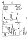
FIG. 14 illustrates avariation 140 of the approach shown inFIG. 4C and utilizes a digital signal processor (DSP) 142 or equivalent circuitry on the transmitportion 144 of thePHY 146. The transmitter (transmit DAC (current-output digital analog converter)) 148 transmits a differential analog signal onlines transformer T1 154.Receiver 156 is coupled to receive the output oftransmitter 148 onlines lines Receiver 156 outputs a digital version of the signal fromtransmitter 148 to aninput 160 ofDSP 142. The digital output online 162 ofDSP 142 constitutes a feedback signal. Test pulses can be initiated, for example, intransmitter 148. These pulses become distorted if there is an effective current imbalance. Thereceiver 156 senses this and in conjunction withDSP 142 causes a correction to the signal so that after a few pulses have been sent and sensed, the transmitportion 144 of thePHY 146 is able to send a predistorted signal that looks perfect or near perfect upon passing through transformer T1 (154). -
FIG. 15 is an electrical schematic diagram which illustrates an example of a circuit for providing current sink/current source capability for the circuits described in more detail above. This is just one example and many other equivalent circuits may be used which are capable of sinking or sourcing current. InFIG. 15 , acontroller 120 is coupled to acurrent imbalance detector 122 which may be of a type adapted for direct measurement of current imbalance (wire side current sensors) or indirect measurement of effective current imbalance (droop detection) as described in more detail above.Controller 120 is coupled to a pair of voltage DACs (digital to analog converters with voltage outputs) 124 and 126. These pass a signal to conventional currentsink circuit block 128 and currentsource circuit block 130, respectively, which are arranged to drive a bias current in either direction. Note that node CTAP may alternatively be grounded or set to some other fixed voltage level. As discussed above, a current sink/source circuit may be located in various places in the circuit to achieve the corrective action described herein and various types of sensing may be used to cause it to act. - While embodiments and applications of this invention have been shown and described, it will now be apparent to those skilled in the art having the benefit of this disclosure that many more modifications than mentioned above are possible. Therefore, the appended claims are intended to encompass within their scope all such modifications as are within the scope of the claims.
- Embodiments of the apparatus and method are further described by way of example in the following numbered clauses:
- 1. A method for compensating for an effective current imbalance in a pair of conductors carrying common mode electrical power, the pair of conductors coupled between a first magnetic device and a second magnetic device, the first magnetic device having a primary winding and a secondary winding, and the second magnetic device having a primary winding and a secondary winding, said pair of conductors coupling said secondary windings of said first and second magnetic devices, the method comprising: detecting the effective current imbalance in the pair of conductors; applying, responsive to said detecting, a direct current bias to the circuit element comprising the pair of conductors and the secondaries of the first and second magnetic devices in a magnitude and direction to compensate for the effective current imbalance.
- 2. The method of
clause 1, wherein said applying occurs through a third winding of the first magnetic device. - 3. The method of
clause 2, wherein the third winding is disposed on the primary side of the first magnetic device. - 4. The method of
clause 2, wherein the third winding is disposed on the secondary side of the first magnetic device. - 5. The method of
clause 1, wherein said detecting senses the effective current imbalance indirectly by monitoring data pulses received through the primary winding of the first magnetic device. - 6. The method of
clause 1, wherein said detecting senses the effective current imbalance indirectly by means of droop detection pulses transmitted by a PHY through the primary winding of the first magnetic device. - 7. The method of
clause 6, wherein a receiver attached to the PHY monitors the droop detection pulses as they are transmitted by a transmitter at the PHY. - 8. The method of
clause 1, wherein said detecting senses the current imbalance directly by measuring current flow through at least two locations of the circuit element and comparing the measurements to create an error signal to drive the magnitude and direction of the direct current bias. - 9. The method of
clause 1, wherein said applying occurs at a node disposed in the circuit element. - 10. The method of clause 8, wherein said applying occurs at a node disposed in the circuit element.
- 11. The method of
clause 2, wherein said detecting senses the effective current imbalance indirectly by monitoring pulses received through the primary winding of the first magnetic device. - 12. The method of
clause 3, wherein said detecting senses the effective current imbalance indirectly by monitoring pulses received through the primary winding of the first magnetic device. - 13. The method of
clause 4, wherein said detecting senses the effective current imbalance indirectly by monitoring pulses received through the primary winding of the first magnetic device. - 14. The method of
clause 2, wherein said detecting senses the effective current imbalance directly by measuring current flow through at least two locations of the circuit element and comparing the measurements to create an error signal to drive the magnitude and direction of the direct current bias. - 15. The method of
clause 3, wherein said detecting senses the effective current imbalance directly by measuring current flow through at least two locations of the circuit element and comparing the measurements to create an error signal to drive the magnitude and direction of the direct current bias. - 16. The method of
clause 4, wherein said detecting senses the effective current imbalance directly by measuring current flow through at least two locations of the circuit element and comparing the measurements to create an error signal to drive the magnitude and direction of the direct current bias. - 17. An apparatus for compensating for an effective current imbalance in a pair of conductors carrying common mode electrical power, the pair of conductors coupled between a first magnetic device and a second magnetic device, the first magnetic device having a primary winding and a secondary winding, and the second magnetic device having a primary winding and a secondary winding, said pair of conductors coupling said secondary windings of said first and second magnetic devices, the apparatus comprising: means for detecting the effective current imbalance in the pair of conductors; means for applying, responsive to said means for detecting, a direct current bias to the circuit element comprising the pair of conductors and the secondaries of the first and second magnetic devices in a magnitude and direction to compensate for the effective current imbalance.
- 18. The apparatus of
clause 17, wherein said means for applying utilizes a third winding of the first magnetic device. - 19. The apparatus of
clause 18, wherein the third winding is disposed on the primary side of the first magnetic device. - 20. The apparatus of
clause 18, wherein the third winding is disposed on the secondary side of the first magnetic device. - 21. The apparatus of
clause 17, wherein said means for detecting senses the effective current imbalance indirectly by monitoring data pulses received through the primary winding of the first magnetic device. - 22. The apparatus of
clause 17, wherein said means for detecting senses the effective current imbalance indirectly by means of droop detection pulses transmitted by a PHY through the primary winding of the first magnetic device. - 23. The apparatus of clause 22, wherein a receiver attached to the PHY monitors the droop detection pulses as they are transmitted by a transmitter at the PHY.
- 24. The apparatus of
clause 17, wherein said means for detecting senses the effective current imbalance directly by measuring current flow through at least two locations of the circuit element and compares the measurements to create an error signal to drive the magnitude and direction of the direct current bias. - 25. The apparatus of
clause 17, wherein said means for applying operates to inject a current at a node disposed in the circuit element. - 26. The apparatus of
clause 24, wherein said means for applying operates to inject a current at a node disposed in the circuit element. - 27. The apparatus of
clause 18, wherein said means for detecting senses the effective current imbalance indirectly by monitoring pulses received through the primary winding of the first magnetic device. - 28. The apparatus of
clause 19, wherein said means for detecting senses the effective current imbalance indirectly by monitoring pulses received through the primary winding of the first magnetic device. - 29. The apparatus of clause 20, wherein said means for detecting senses the effective current imbalance indirectly by monitoring pulses received through the primary winding of the first magnetic device.
- 30. The apparatus of
clause 18, wherein said means for detecting senses the effective current imbalance directly by measuring current flow through at least two locations of the circuit element and compares the measurements to create an error signal to drive the magnitude and direction of the direct current bias. - 31. The apparatus of
clause 19, wherein said means for detecting senses the effective current imbalance directly by measuring current flow through at least two locations of the circuit element and compares the measurements to create an error signal to drive the magnitude and direction of the direct current bias. - 32. The apparatus of clause 20, wherein said means for detecting senses the effective current imbalance directly by measuring current flow through at least two locations of the circuit element and compares the measurements to create an error signal to drive the magnitude and direction of the direct current bias.
- 33. A system for compensating for an effective current imbalance in a pair of conductors carrying common mode electrical power, the pair of conductors coupled between a first magnetic device and a second magnetic device, the first magnetic device having a primary winding and a secondary winding, and the second magnetic device having a primary winding and a secondary winding, said pair of conductors coupling said secondary windings of said first and second magnetic devices, the system comprising: circuitry for detecting the effective current imbalance in the pair of conductors; circuitry for applying, responsive to said circuitry for detecting, a direct current bias to the circuit element comprising the pair of conductors and the secondaries of the first and second magnetic devices in a magnitude and direction to compensate for the effective current imbalance.
- 34. The system of clause 33, wherein said circuitry for applying utilizes a third winding of the first magnetic device.
- 35. The system of clause 34, wherein the third winding is disposed on the primary side of the first magnetic device.
- 36. The system of clause 34, wherein the third winding is disposed on the secondary side of the first magnetic device.
- 37. The system of clause 33, wherein said circuitry for detecting senses the effective current imbalance indirectly by monitoring data pulses received through the primary winding of the first magnetic device.
- 38. The system of clause 33, wherein said circuitry for detecting senses the effective current imbalance indirectly by means of droop detection pulses transmitted by a PHY through the primary winding of the first magnetic device.
- 39. The system of clause 38, wherein a receiver attached to the PHY monitors the droop detection pulses as they are transmitted by a transmitter at the PHY.
- 40. The system of clause 33, wherein said circuitry for detecting senses the effective current imbalance directly by measuring current flow through at least two locations of the circuit element and compares the measurements to create an error signal to drive the magnitude and direction of the direct current bias.
- 41. The system of clause 33, wherein said circuitry for applying operates to inject a current at a node disposed in the circuit element.
- 42. The system of clause 40, wherein said circuitry for applying operates to inject a current at a node disposed in the circuit element.
- 43. The system of clause 34, wherein said circuitry for detecting senses the effective current imbalance indirectly by monitoring pulses received through the primary winding of the first magnetic device.
- 44. The system of clause 35, wherein said circuitry for detecting senses the effective current imbalance indirectly by monitoring pulses received through the primary winding of the first magnetic device.
- 45. The system of clause 36, wherein said circuitry for detecting senses the effective current imbalance indirectly by monitoring pulses received through the primary winding of the first magnetic device.
- 46. The system of clause 34, wherein said circuitry for detecting senses the effective current imbalance directly by measuring current flow through at least two locations of the circuit element and compares the measurements, to create an error signal to drive the magnitude and direction of the direct current bias.
- 47. The system of clause 35, wherein said circuitry for detecting senses the effective current imbalance directly by measuring current flow through at least two locations of the circuit element and compares the measurements to create an error signal to drive the magnitude and direction of the direct current bias.
- 48. The system of clause 36, wherein said circuitry for detecting senses the effective current imbalance directly by measuring current flow through at least two locations of the circuit element and compares the measurements to create an error signal to drive the magnitude and direction of the direct current bias.
- 49. A power sourcing equipment (PSE) apparatus, comprising: a first magnetic device having a primary winding and a secondary winding; a coupler for receiving a pair of conductors, the coupler coupled to the secondary winding of the first magnetic device; power sourcing circuitry coupled to apply a common mode inline power voltage signal to the secondary of the first magnetic device; circuitry for detecting an effective current imbalance in the pair of conductors; and circuitry for applying, responsive to said circuitry for detecting, a direct current bias to a circuit element comprising the coupler and the secondary of the first magnetic device in a magnitude and direction to compensate for the current imbalance.
- 50. The PSE of clause 49, wherein said circuitry for applying utilizes a third winding of the first magnetic device.
- 51. The PSE of
clause 50, wherein the third winding is disposed on the primary side of the first magnetic device. - 52. The PSE of
clause 50, wherein the third winding is disposed on the secondary side of the first magnetic device. - 53. The PSE of clause 49, wherein said circuitry for detecting senses the effective current imbalance indirectly by monitoring data pulses received through the primary winding of the first magnetic device.
- 54. The PSE of clause 49, wherein said circuitry for detecting senses the effective current imbalance indirectly by means of droop detection pulses transmitted by a PHY through the primary winding of the first magnetic device.
- 55. The PSE of
clause 54, wherein a receiver attached to the PHY monitors the droop detection pulses as they are transmitted by a transmitter at the PHY. - 56. The PSE of clause 49, wherein said circuitry for detecting senses the effective current imbalance directly by measuring current flow through at least two locations of the circuit element and compares the measurements to create an error signal to drive the magnitude and direction of the direct current bias.
- 57. The PSE of clause 49, wherein said circuitry for applying operates to inject a current at a node disposed in the circuit element.
- 58. The PSE of
clause 56, wherein said circuitry for applying operates to inject a current at a node disposed in the circuit element. - 59. The PSE of
clause 50, wherein said circuitry for detecting senses the effective current imbalance indirectly by monitoring pulses received through the primary winding of the first magnetic device. - 60. The PSE of
clause 51, wherein said circuitry for detecting senses the effective current imbalance indirectly by monitoring pulses received through the primary winding of the first magnetic device. - 61. The PSE of
clause 52, wherein said circuitry for detecting senses the effective current imbalance indirectly by monitoring pulses received through the primary winding of the first magnetic device. - 62. The PSE of
clause 50, wherein said circuitry for detecting senses the effective current imbalance directly by measuring current flow through at least two locations of the circuit element and compares the measurements to create an error signal to drive the magnitude and direction of the direct current bias. - 63. The PSE of
clause 51 , wherein said circuitry for detecting senses the effective current imbalance directly by measuring current flow through at least two locations of the circuit element and compares the measurements to create an error signal to drive the magnitude and direction of the direct current bias. - 64. The PSE of
clause 52, wherein said circuitry for detecting senses the effective current imbalance directly by measuring current flow through at least two locations of the circuit element and compares the measurements to create an error signal to drive the magnitude and direction of the direct current bias. - 65. A powered device (PD) apparatus, comprising: a second magnetic device having a primary winding and a secondary winding; a coupler for receiving a pair of conductors coupled to a secondary winding of a remote first magnetic device, the coupler coupled to the secondary winding of the second magnetic device; powered device circuitry coupled to receive a common mode inline power voltage signal from the secondary of the second magnetic device; circuitry for detecting an effective current imbalance in the pair of conductors; and circuitry for applying, responsive to said circuitry for detecting, a direct current bias to a circuit element comprising the coupler and the secondary of the second magnetic device in a magnitude and direction to compensate for the effective current imbalance.
- 66. The PD of clause 65, wherein said circuitry for applying utilizes a third winding of the second magnetic device.
- 67. The PD of
clause 66, wherein the third winding is disposed on the primary side of the second magnetic device. - 68. The PD of
clause 66, wherein the third winding is disposed on the secondary side of the second magnetic device. - 69. The PD of clause 65, wherein said circuitry for detecting senses the effective current imbalance indirectly by monitoring data pulses received through the primary winding of the second magnetic device.
- 70. The PD of clause 65, wherein said circuitry for detecting senses the effective current imbalance indirectly by means of droop detection pulses transmitted by a PHY through the primary winding of the second magnetic device.
- 71. The PD of
clause 70, wherein a receiver attached to the PHY monitors the droop detection pulses as they are transmitted by a transmitter at the PHY. - 72. The PD of clause 65, wherein said circuitry for detecting senses the effective current imbalance directly by measuring current flow through at least two locations of the circuit element and compares the measurements to create an error signal to drive the magnitude and direction of the direct current bias.
- 73. The PD of clause 65, wherein said circuitry for applying operates to inject a current at a node disposed in the circuit element.
- 74. The PD of
clause 72, wherein said circuitry for applying operates to inject a current at a node disposed in the circuit element. - 75. The PD of
clause 66, wherein said circuitry for detecting senses the effective current imbalance indirectly by monitoring pulses received through the primary winding of the second magnetic device. - 76. The PD of clause 67, wherein said circuitry for detecting senses the effective current imbalance indirectly by monitoring pulses received through the primary winding of the second magnetic device.
- 77. The PD of
clause 68, wherein said circuitry for detecting senses the effective current imbalance indirectly by monitoring pulses received through the primary winding of the second magnetic device. - 78. The PD of
clause 66, wherein said circuitry for detecting senses the effective current imbalance directly by measuring current flow through at least two locations of the circuit element and compares the measurements to create an error signal to drive the magnitude and direction of the direct current bias. - 79. The PD of clause 67, wherein said circuitry for detecting senses the effective current imbalance directly by measuring current flow through at least two locations of the circuit element and compares the measurements to create an error signal to drive the magnitude and direction of the direct current bias.
- 80. The PD of
clause 68, wherein said circuitry for detecting senses the effective current imbalance directly by measuring current flow through at least two locations of the circuit element and compares the measurements to create an error signal to drive the magnitude and direction of the direct current bias. - 81. A method for compensating for an effective current imbalance in a pair of conductors carrying common mode electrical power, the pair of conductors coupled between a first magnetic device and a second magnetic device, the first magnetic device associated with power sourcing equipment (PSE) and having a primary winding and a secondary winding, and the second magnetic device associated with a powered device (PD) and having a primary winding and a secondary winding, said pair of conductors coupling said secondary windings of said first and second magnetic devices, the method comprising: conducting an auto-negotiation between the PSE and the PD to select which of the PSE and the PD will current imbalance correct the current in the pair of conductors; detecting at the selected one of the PSE and the PD the effective current imbalance in the pair of conductors; applying at the selected one of the PSE and the PD5responsive to said detecting, a direct current bias to the circuit element comprising the pair of conductors and the secondaries of the first and second magnetic devices in a magnitude and direction to compensate for the effective current imbalance.
- 82. A method for compensating for an effective current imbalance in a pair of conductors carrying common mode electrical power, the pair of conductors coupled between a first magnetic device and a second magnetic device, the first magnetic device associated with power sourcing equipment (PSE) and having a primary winding and a secondary winding, and the second magnetic device associated with a powered device (PD) and having a primary winding and a secondary winding, said pair of conductors coupling said secondary windings of said first and second magnetic devices, the method comprising: conducting a time domain reflectometer measurement to measure the length of the pair of conductors; detecting (if the measured length is less than a predetermined length) the effective current imbalance in the pair of conductors; applying (if the measured length is less than a predetermined length), responsive to said detecting, a direct current bias to the circuit element comprising the pair of conductors and the secondaries of the first and second magnetic devices in a magnitude and direction to compensate for the effective current imbalance.
- 83. A method for compensating for an effective current imbalance in a pair of conductors carrying common mode electrical power, the pair of conductors coupled between a first magnetic device and a second magnetic device, the first magnetic device having a primary winding and a secondary winding, and the second magnetic device having a primary winding and a secondary winding, said pair of conductors coupling said secondary windings of said first and second magnetic devices, the method comprising: detecting the effective current imbalance; applying, responsive to said detecting, a predistorted signal to a primary of the first magnetic device, predistortion in the applied predistorted signal compensating for the effective current imbalance.
- 84. The method of clause 83, wherein said detecting is performed with a receiver wired to receive a differential signal transmitted into the primary of the first magnetic device.
- 85. The method of
clause 84, wherein said applying is performed with a digital signal processor (DSP) receiving an input from the receiver. - 86. A method for compensating for an effective current imbalance in a pair of conductors carrying common mode electrical power, the pair of conductors coupled between a first magnetic device and a second magnetic device, the first magnetic device having a primary winding and a secondary winding, and the second magnetic device having a primary winding and a secondary winding, said pair of conductors coupling said secondary windings of said first and second magnetic devices, the method comprising: detecting the effective current imbalance with first equipment coupled to the primary of the first magnetic device; communicating between the first equipment and second equipment coupled to the primary of the second magnetic device; and correcting for the imbalance at the primary of the first magnetic device responsive to said detecting and said communicating.
- 87. A method for compensating for an effective current imbalance in a pair of conductors carrying common mode electrical power, the pair of conductors coupled between a first magnetic device and a second magnetic device, the first magnetic device having a primary winding and a secondary winding, and the second magnetic device having a primary winding and a secondary winding, said pair of conductors coupling said secondary windings of said first and second magnetic devices, the method comprising: detecting the effective current imbalance with first equipment coupled to the primary of the first magnetic device and with second equipment coupled to the primary of the second magnetic device; communicating between the first equipment and the second equipment; and correcting for the imbalance at one or both of the primary of the first magnetic device and the primary of the second magnetic device in response to said detecting and said communicating.
Claims (12)
- A method for compensating an imbalance in a flow of current in a pair of conductors (150) carrying common mode electrical power between a first magnetic device (154) and a second magnetic device, the first magnetic device (154) having a primary winding (152) and a secondary winding and the second magnetic device having a primary winding and a secondary winding, wherein the imbalance in the flow of current in the pair of conductors (150) causes distortion of a differential signal (158) transmitted along the pair of conductors (150), the method being characterized by comprising the steps of:detecting the imbalance in the flow of current in the pair of conductors (150);applying a predistortion to the differential signal (158) prior to the differential signal (158) being transmitted to the primary winding (152) of the first magnetic device (154), the predistortion providing compensation for the distortion that would be caused to the differential signal (158) by the detected imbalance in the flow of current in the pair of conductors (150); andtransmitting the predistorted differential signal (158) to the primary winding (152) of the first magnetic device (154).
- The method of claim 1, wherein detecting the imbalance in the flow of current in the pair of conductors comprises:receiving, by a receiver (156), the differential signal (158) as transmitted to the primary winding (152) of the first magnetic device (154); anddetecting, by the receiver (156), the imbalance in the flow of current based on the received differential signal (158).
- The method of claim 2, wherein applying the predistortion to the differential signal prior to the differential signal (158) being transmitted to the primary winding (152) of the first magnetic device (154) comprises:receiving, by a Digital Signal Processor, DSP, (142) a digital version of the differential signal from the receiver (156); andapplying, by the DSP (142) and based on the digital version of the differential signal from the receiver (156), the predistortion to the differential signal prior to the differential signal (158) being transmitted to the primary winding (152) of the first magnetic device (154).
- The method of any of claims 1, 2, or 3, wherein detecting the imbalance in the flow of current in the pair of conductors (150) comprises:receiving a test pulse of the differential signal (158) as transmitted to the primary winding (152) of the first magnetic device (154); andsensing a distortion of the test pulse when an imbalance in the flow of current in the pair of conductors (150) exists.
- The method of claim 4, wherein sensing the distortion of the test pulse when the imbalance in the flow of current in the pair of conductors (150) exists comprises:comparing a characteristic of the test pulse with a characteristic of an ideal pulse;generating a difference error signal from the difference between the test pulse and the ideal pulse, based on the comparison of the characteristic of the test pulse and the characteristic of the ideal pulse; andcorrecting the test pulse of the differential signal (162), based on the difference error signal, to compensate for the detected imbalance in the flow of current in the pair of conductors.
- The method of claim 5, wherein comparing a characteristic of the test pulse with a characteristic of an ideal pulse comprises:measuring a peak amplitude of the test pulse at an end of the test pulse; andcomparing the peak amplitude of the test pulse at the end of the test pulse with a peak amplitude of the ideal pulse at an end of the ideal pulse.
- An apparatus, comprising:a Physical Layer, PHY, (146) having transmit portion circuit (144) and receive portion circuitry, wherein the transmit portion circuitry being characterized by comprising:means for detecting an imbalance in a flow of current in a pair of conductors (150) carrying common mode electrical power between a first magnetic device (154) and a second magnetic device, the first magnetic device (154) having a primary winding (152) and a secondary winding and the second magnetic device having a primary winding and a secondary winding, wherein the imbalance in the flow of current in the pair of conductors (150) causes distortion of a differential signal (158) transmitted along the pair of conductors (150),; andmeans for applying a predistortion to the differential signal (158) prior to the differential signal (158) being transmitted to the primary winding (152) of the first magnetic device (154), the predistortion compensating for the distortion that would be caused to the differential signal (158) by the detected imbalance in the flow of current in the pair of conductors (150); andmeans for transmitting the predistorted differential signal (158) to the primary winding (152) of the first magnetic device (154).
- The apparatus of claim 7, wherein the means for detecting comprises a receiver (156) that, when detecting the imbalance in the flow of current in the pair of conductors (150), is configured to:receive the differential signal (158) as transmitted to the primary winding (152) of the first magnetic device (154); anddetect the imbalance in the flow of current based on the received differential signal (158).
- The apparatus of claim 8, wherein the means for applying a predistortion to the differential signal comprises a Digital Signal Processor, DSP, (142) that, when applying the predistortion to the differential signal (158) prior to the differential signal (158) being transmitted to the primary winding (152) of the first magnetic device (154), is configured to:receive a digital version of the differential signal from the receiver (156); andapply, based on the digital version of the differential signal from the receiver, the predistortion to the differential signal (158) prior to the differential signal (158) being transmitted to the primary winding (152) of the first magnetic device (154).
- The apparatus of any of claims 7 to 9, wherein the means for detecting the imbalance in the flow of current in the pair of conductors (150), is configured to:receive a test pulse of the differential signal (158) as transmitted to the primary winding (152) of the first magnetic device (154); andsense a distortion of the test pulse when an imbalance in the flow of current in the pair of conductors (150) exists.
- The apparatus of claim 10, wherein when sensing the distortion of the test pulse when the imbalance in the flow of current in the pair of conductors (152) exists, the transmit portion circuitry is configured to:compare a characteristic of the test pulse with a characteristic of an ideal pulse;generate a difference error signal from the difference between the test pulse and the ideal pulse, based on the comparison of the characteristic of the test pulse and the characteristic of the ideal pulse; andcorrect the test pulse of the differential signal (162), based on the difference error signal, to compensate for the detected imbalance in the flow of current in the pair of conductors (150).
- The apparatus of claim 11, wherein when comparing a characteristic of the test pulse with a characteristic of an ideal pulse, the transmit portion circuitry is configured to:measure a peak amplitude of the test pulse at an end of the test pulse; andcompare the peak amplitude of the test pulse at the end of the test pulse with a peak amplitude of the ideal pulse at an end of the ideal pulse.
Applications Claiming Priority (2)
| Application Number | Priority Date | Filing Date | Title |
|---|---|---|---|
| US10/981,202 US7457252B2 (en) | 2004-11-03 | 2004-11-03 | Current imbalance compensation for magnetics in a wired data telecommunications network |
| EP05809915A EP1813055B1 (en) | 2004-11-03 | 2005-10-07 | Phy-based current imbalance compensation for magnetics in a wired data telecommunications network |
Related Parent Applications (1)
| Application Number | Title | Priority Date | Filing Date |
|---|---|---|---|
| EP05809915.1 Division | 2005-10-07 |
Publications (2)
| Publication Number | Publication Date |
|---|---|
| EP2222017A1 EP2222017A1 (en) | 2010-08-25 |
| EP2222017B1 true EP2222017B1 (en) | 2012-02-29 |
Family
ID=35811775
Family Applications (2)
| Application Number | Title | Priority Date | Filing Date |
|---|---|---|---|
| EP05809915A Not-in-force EP1813055B1 (en) | 2004-11-03 | 2005-10-07 | Phy-based current imbalance compensation for magnetics in a wired data telecommunications network |
| EP10166072A Active EP2222017B1 (en) | 2004-11-03 | 2005-10-07 | Phy-based current imbalance compensation for magnetics in a wired data telecommunications network |
Family Applications Before (1)
| Application Number | Title | Priority Date | Filing Date |
|---|---|---|---|
| EP05809915A Not-in-force EP1813055B1 (en) | 2004-11-03 | 2005-10-07 | Phy-based current imbalance compensation for magnetics in a wired data telecommunications network |
Country Status (5)
| Country | Link |
|---|---|
| US (2) | US7457252B2 (en) |
| EP (2) | EP1813055B1 (en) |
| AT (2) | ATE476029T1 (en) |
| DE (1) | DE602005022611D1 (en) |
| WO (1) | WO2006052360A1 (en) |
Families Citing this family (46)
| Publication number | Priority date | Publication date | Assignee | Title |
|---|---|---|---|---|
| GB0403932D0 (en) * | 2004-02-21 | 2004-03-24 | Koninkl Philips Electronics Nv | Improving image quality in a 3D image display device |
| US7793137B2 (en) * | 2004-10-07 | 2010-09-07 | Cisco Technology, Inc. | Redundant power and data in a wired data telecommunincations network |
| US7719992B1 (en) * | 2004-07-14 | 2010-05-18 | Cisco Tchnology, Ink. | System for proactive time domain reflectometry |
| US8831211B2 (en) * | 2004-11-19 | 2014-09-09 | Linear Technology Corporation | Common-mode data transmission for power over ethernet system |
| US7656956B2 (en) * | 2005-01-14 | 2010-02-02 | Motorola, Inc. | Data, power and supervisory signaling over twisted pairs |
| US7827418B2 (en) * | 2005-01-25 | 2010-11-02 | Linear Technology Corporation | Controlling power distribution among multiple wires in communication cable |
| US20060212724A1 (en) * | 2005-03-15 | 2006-09-21 | Dwelley David M | System and method for supporting operations of advanced power over ethernet system |
| US20060251188A1 (en) * | 2005-03-28 | 2006-11-09 | Akros Silicon, Inc. | Common-mode suppression circuit for emission reduction |
| US7685452B2 (en) * | 2005-03-28 | 2010-03-23 | Akros Silicon Inc. | Method for high voltage power feed on differential cable pairs from a network attached power sourcing device |
| US7560825B2 (en) * | 2006-04-11 | 2009-07-14 | Akros Silicon, Inc. | Network devices for separating power and data signals |
| WO2007121148A2 (en) * | 2006-04-11 | 2007-10-25 | Akros Silicon, Inc. | Network devices for separating power and data signals |
| US20080048779A1 (en) * | 2006-05-16 | 2008-02-28 | Crawley Philip J | Active emi suppression circuit |
| US8643218B2 (en) | 2006-06-02 | 2014-02-04 | Broadcom Corporation | Minimizing saturation caused by power transfer in a communication system transformer |
| US7697251B2 (en) * | 2006-09-06 | 2010-04-13 | Cisco Technology, Inc. | Powered communications interface with DC current imbalance compensation |
| US8576873B2 (en) * | 2006-11-30 | 2013-11-05 | Broadcom Corporation | System and method for controlling power delivered to a powered device based on channel impediments |
| US7664972B2 (en) * | 2006-12-19 | 2010-02-16 | Broadcom Corporation | System and method for controlling power delivered to a powered device based on cable characteristics |
| EP1936875B1 (en) * | 2006-12-19 | 2016-03-09 | Broadcom Corporation | System and method for diagnosing a cabling infrastructure using a PHY |
| US7738387B2 (en) | 2007-01-17 | 2010-06-15 | Broadcom Corporation | System and method for diagnosing a cabling infrastructure using a PHY |
| US7921307B2 (en) * | 2007-03-27 | 2011-04-05 | Cisco Technology, Inc. | Methods and apparatus providing advanced classification for power over Ethernet |
| US7777636B2 (en) * | 2007-03-29 | 2010-08-17 | Broadcom Corporation | System and method for continual cable thermal monitoring using cable characteristic considerations in power over Ethernet |
| US7737704B2 (en) * | 2007-06-12 | 2010-06-15 | Broadcom Corporation | System and method for using a PHY to locate a thermal signature in a cable plant for diagnostic, enhanced, and higher power applications |
| US8611235B2 (en) * | 2007-06-14 | 2013-12-17 | Cisco Technology, Inc. | Extended reach data network |
| US7696636B2 (en) | 2007-08-24 | 2010-04-13 | Broadcom Corporation | Midspan powering in a Power over Ethernet system |
| US7975153B2 (en) | 2007-09-25 | 2011-07-05 | Broadcom Corporation | Transmission impedance for four-pair midspan powering in a power over ethernet application |
| US7971075B2 (en) | 2007-09-25 | 2011-06-28 | Broadcom Corporation | Four-pair midspan powering with a splitter in a power over ethernet application |
| US7851938B2 (en) | 2007-09-25 | 2010-12-14 | Broadcom Corporation | Midspan powering without the use of data transformers in a power over Ethernet application |
| ES2321792B1 (en) * | 2007-10-03 | 2010-03-04 | Diseño De Sistemas En Silicio S.A. | MULTIINJECTION VOLTAGE DEVICE ON MULTIPLE DRIVERS. |
| US20090097401A1 (en) * | 2007-10-12 | 2009-04-16 | Wael William Diab | Method and system for configurable data rate thresholds for energy efficient ethernet |
| US7902694B2 (en) * | 2007-11-08 | 2011-03-08 | Cisco Technology, Inc. | Dynamic current limits |
| KR101173751B1 (en) * | 2007-12-04 | 2012-08-13 | 미쓰비시덴키 가부시키가이샤 | Ac motor controller |
| WO2009124069A1 (en) * | 2008-04-02 | 2009-10-08 | Marvell World Trade Ltd. | Reduced power transmission |
| US9712459B1 (en) | 2010-01-27 | 2017-07-18 | Marvell International Ltd. | Low-to-high speed cut-through communication |
| US8787964B2 (en) * | 2010-06-23 | 2014-07-22 | MindTree Limited | Integrated radio frequency front-end circuit |
| US8823402B2 (en) * | 2011-11-23 | 2014-09-02 | Broadcom Corporation | Cable resistance determination in high-power PoE networks |
| US20140040641A1 (en) * | 2012-08-03 | 2014-02-06 | Broadcom Corporation | Cable Imbalance Diagnostics Between Channels That Include Wire Pairs for Power Over Ethernet Transmission |
| FR2998430B1 (en) * | 2012-11-20 | 2016-01-08 | Thales Sa | ELECTRICAL POWER TRANSMISSION ON DATA TRANSMISSION CABLE |
| US9014248B2 (en) * | 2013-01-31 | 2015-04-21 | Broadcom Corporation | BASE-T common mode testing in an Ethernet subsystem |
| US9385929B2 (en) | 2013-02-26 | 2016-07-05 | Cisco Technology, Inc. | Methods and devices for performing dynamic droop compensation |
| US9337905B2 (en) * | 2013-07-01 | 2016-05-10 | Texas Instruments Incorporated | Inductive structures with reduced emissions and interference |
| JP2015043508A (en) * | 2013-08-26 | 2015-03-05 | オンキヨー株式会社 | Signal transmission circuit |
| US9819271B2 (en) * | 2013-09-30 | 2017-11-14 | O2Micro, Inc. | Power converters |
| CN104377677B (en) * | 2014-11-07 | 2017-02-15 | 南京信息工程大学 | Surge protection device of end-span method active Ethernet |
| US10135626B2 (en) * | 2015-04-14 | 2018-11-20 | Avago Technologies General Ip (Singapore) Pte. Ltd. | Power coupling circuits for single-pair ethernet with automotive applications |
| US10177713B1 (en) * | 2016-03-07 | 2019-01-08 | Ali Tasdighi Far | Ultra low power high-performance amplifier |
| US10601525B2 (en) | 2018-04-20 | 2020-03-24 | Arm Limited | Power distribution for functional circuit blocks |
| CN111092445B (en) * | 2018-10-24 | 2021-10-26 | 华为技术有限公司 | Signal reliability detection method, PSE chip, CPU chip and PoE device |
Family Cites Families (75)
| Publication number | Priority date | Publication date | Assignee | Title |
|---|---|---|---|---|
| US580860A (en) * | 1897-04-20 | Refill for cisterns | ||
| US3380801A (en) | 1966-07-08 | 1968-04-30 | Exxon Production Research Co | Separation of cobalt from nickel |
| US4835737A (en) | 1986-07-21 | 1989-05-30 | American Telephone And Telegraph Company, At&T Bell Laboratories | Method and apparatus for controlled removal and insertion of circuit modules |
| US5038320A (en) | 1987-03-13 | 1991-08-06 | International Business Machines Corp. | Computer system with automatic initialization of pluggable option cards |
| US5237511A (en) | 1990-10-29 | 1993-08-17 | Westronic, Inc. | Distribution automation smart remote terminal unit |
| US5122691A (en) | 1990-11-21 | 1992-06-16 | Balu Balakrishnan | Integrated backplane interconnection architecture |
| US5289359A (en) | 1991-02-13 | 1994-02-22 | Charles Industries, Limited | DC-DC power converter including sensing means for providing an output when the reserve power of the converter falls below a predetermined amount for a given input voltage |
| US5268592A (en) | 1991-02-26 | 1993-12-07 | International Business Machines Corporation | Sequential connector |
| US5148144A (en) | 1991-03-28 | 1992-09-15 | Echelon Systems Corporation | Data communication network providing power and message information |
| JP2905616B2 (en) | 1991-05-20 | 1999-06-14 | シャープ株式会社 | Communication terminal device |
| JPH0821015B2 (en) | 1992-01-20 | 1996-03-04 | インターナショナル・ビジネス・マシーンズ・コーポレイション | Computer and system reconfiguring apparatus and method thereof |
| CA2097449C (en) | 1992-06-05 | 1998-09-15 | Satosi Sakuragi | Telephone line power utility circuit |
| US5406260A (en) | 1992-12-18 | 1995-04-11 | Chrimar Systems, Inc. | Network security system for detecting removal of electronic equipment |
| GB9325594D0 (en) | 1993-12-14 | 1994-02-16 | Amp Great Britain | Multi-port modular jack assembly |
| US5608792A (en) | 1994-04-13 | 1997-03-04 | British Telecommunications Public Limited Company | Apparatus for drawing and processing electrical power from a communications line |
| US5613130A (en) | 1994-11-10 | 1997-03-18 | Vadem Corporation | Card voltage switching and protection |
| AU4841396A (en) | 1995-01-27 | 1996-08-14 | Itecom, Incorporated | Multimedia system having central power source and distribution subsystem |
| US5726506A (en) | 1995-06-05 | 1998-03-10 | Alantec Corporation | Hot insertion power arrangement |
| JP3407838B2 (en) | 1995-09-05 | 2003-05-19 | ソニー株式会社 | Video on demand system |
| US5758102A (en) | 1996-01-11 | 1998-05-26 | International Business Machines Corporation | Soft switching circuit for use on backplane |
| US5726901A (en) | 1996-01-25 | 1998-03-10 | Dell Usa, L.P. | System for reporting computer energy consumption |
| US5639267A (en) | 1996-01-26 | 1997-06-17 | Maxconn Incorporated | Modular jack assembly |
| US5793987A (en) | 1996-04-18 | 1998-08-11 | Cisco Systems, Inc. | Hot plug port adapter with separate PCI local bus and auxiliary bus |
| US5742513A (en) | 1996-05-15 | 1998-04-21 | Abb Power T&D Company Inc. | Methods and systems for automatic testing of a relay |
| US5809256A (en) | 1996-06-11 | 1998-09-15 | Data General Corporation | Soft power switching for hot installation and removal of circuit boards in a computer system |
| US5790873A (en) | 1996-07-23 | 1998-08-04 | Standard Microsystems Corporation | Method and apparatus for power supply switching with logic integrity protection |
| US5775946A (en) | 1996-08-23 | 1998-07-07 | Amphenol Corporation | Shielded multi-port connector and method of assembly |
| US5796185A (en) | 1996-10-15 | 1998-08-18 | Sony Corporation | Circuit card present sense and protective power supply inhibit for airborne application of ATM switch unit |
| US5790391A (en) | 1996-11-29 | 1998-08-04 | General Signal Corporation | Standby power system |
| TW364679U (en) | 1996-12-26 | 1999-07-11 | Hon Hai Prec Ind Co Ltd | Plug slot connector terminal |
| US6009317A (en) * | 1997-01-17 | 1999-12-28 | Ericsson Inc. | Method and apparatus for compensating for imbalances between quadrature signals |
| US6068520A (en) | 1997-03-13 | 2000-05-30 | Berg Technology, Inc. | Low profile double deck connector with improved cross talk isolation |
| US5884086A (en) | 1997-04-15 | 1999-03-16 | International Business Machines Corporation | System and method for voltage switching to supply various voltages and power levels to a peripheral device |
| US5834925A (en) | 1997-05-08 | 1998-11-10 | Cisco Technology, Inc. | Current sharing power supplies with redundant operation |
| US5994998A (en) | 1997-05-29 | 1999-11-30 | 3Com Corporation | Power transfer apparatus for concurrently transmitting data and power over data wires |
| US5991885A (en) | 1997-06-11 | 1999-11-23 | Clarinet Systems, Inc. | Method and apparatus for detecting the presence of a remote device and providing power thereto |
| US6162089A (en) | 1997-12-30 | 2000-12-19 | The Whitaker Corporation | Stacked LAN connector |
| US6087861A (en) * | 1998-02-11 | 2000-07-11 | International Business Machines Corporation | Data network drivers including balanced current supplies and related methods |
| US6036547A (en) | 1998-03-05 | 2000-03-14 | Berg Technology, Inc. | Double deck gang jack exhibiting suppressed mutual crosstalk |
| US6134666A (en) | 1998-03-12 | 2000-10-17 | Cisco Technology, Inc. | Power supervisor for electronic modular system |
| US6115468A (en) | 1998-03-26 | 2000-09-05 | Cisco Technology, Inc. | Power feed for Ethernet telephones via Ethernet link |
| US6033266A (en) | 1998-08-31 | 2000-03-07 | The Whitaker Corporation | Modular connector with preload and beam length reduction features |
| US6643566B1 (en) | 1999-01-12 | 2003-11-04 | Powerdsine Ltd. | System for power delivery over data communication cabling infrastructure |
| US6099349A (en) | 1999-02-23 | 2000-08-08 | Amphenol Corporation | Dual multiport RJ connector arrangement |
| US6218930B1 (en) | 1999-03-10 | 2001-04-17 | Merlot Communications | Apparatus and method for remotely powering access equipment over a 10/100 switched ethernet network |
| US6233128B1 (en) | 1999-03-29 | 2001-05-15 | George A. Spencer | Data retention in a circuit breaker |
| US6310781B1 (en) | 1999-03-31 | 2001-10-30 | Cisco Technology, Inc. | Connection pin layout for connecting integrated magnetics modules to a printed circuit board |
| JP2001008452A (en) * | 1999-06-21 | 2001-01-12 | Sony Corp | Power supply device |
| US6762675B1 (en) | 1999-09-27 | 2004-07-13 | Cisco Technology, Inc. | Method and apparatus for remote powering of device connected to network |
| US6396392B1 (en) | 2000-05-23 | 2002-05-28 | Wire21, Inc. | High frequency network communications over various lines |
| US6701443B1 (en) | 2000-06-19 | 2004-03-02 | Cisco Technology, Inc. | Methods and apparatus for discovering a powerability condition of a computer network |
| US6541878B1 (en) | 2000-07-19 | 2003-04-01 | Cisco Technology, Inc. | Integrated RJ-45 magnetics with phantom power provision |
| US7340405B1 (en) | 2000-09-08 | 2008-03-04 | Sabre Inc. | Method and system for developing optimized schedules |
| TWI279972B (en) * | 2000-10-02 | 2007-04-21 | Omron Tateisi Electronics Co | Electric power system |
| US6448899B1 (en) | 2000-10-25 | 2002-09-10 | Nortel Networks Limited | Power indicating ethernet outlet and method therefor |
| US6804351B1 (en) | 2000-11-09 | 2004-10-12 | Cisco Technology, Inc. | Method and apparatus for detecting a compatible phantom powered device using common mode signaling |
| US6963321B2 (en) * | 2001-05-09 | 2005-11-08 | Clare Micronix Integrated Systems, Inc. | Method of providing pulse amplitude modulation for OLED display drivers |
| US6577258B2 (en) * | 2001-10-01 | 2003-06-10 | Nokia Corporation | Adaptive sigma-delta data converter for mobile terminals |
| US7089126B2 (en) | 2001-11-06 | 2006-08-08 | Intel Corporation | Diode discovery power level detection |
| US6958699B1 (en) | 2001-12-18 | 2005-10-25 | Cisco Technology, Inc. | Signal-disruption detection in powered networking systems |
| US7519000B2 (en) | 2002-01-30 | 2009-04-14 | Panduit Corp. | Systems and methods for managing a network |
| US6986071B2 (en) | 2002-02-01 | 2006-01-10 | Powerdsine, Ltd. | Detecting network power connection status using AC signals |
| EP1495516A1 (en) | 2002-04-10 | 2005-01-12 | Powerdsine Limited | Active local area network connector |
| US7005861B1 (en) * | 2002-06-07 | 2006-02-28 | Marvell International Ltd. | Cable tester |
| AU2003274634A1 (en) | 2002-10-15 | 2004-05-04 | Powerdsine Ltd. | Direct current power pooling |
| TW589796B (en) * | 2002-12-06 | 2004-06-01 | Airoha Tech Corp | An automatic adjustment system for source current and sink current mismatch |
| US8098681B2 (en) | 2003-01-29 | 2012-01-17 | Avaya Inc. | Method and apparatus for dynamic termination of unused wired connection |
| US7154381B2 (en) | 2003-05-23 | 2006-12-26 | Sonos, Inc. | System and method for operating a sensed power device over data wiring |
| US7849343B2 (en) | 2003-06-10 | 2010-12-07 | Microsemi Corp. - Analog Mixed Signal Group Ltd. | Pre-detection of powered devices |
| US7145439B2 (en) | 2003-10-16 | 2006-12-05 | Powerdsine, Ltd. | Powered device interface circuit |
| US7460889B2 (en) | 2003-10-16 | 2008-12-02 | Microsemi Corp.—Analog Mixed Signal Group Ltd. | High power classification for power over Ethernet |
| US7141933B2 (en) * | 2003-10-21 | 2006-11-28 | Microsemi Corporation | Systems and methods for a transformer configuration for driving multiple gas discharge tubes in parallel |
| US7356588B2 (en) | 2003-12-16 | 2008-04-08 | Linear Technology Corporation | Circuits and methods for detecting the presence of a powered device in a powered network |
| US7162377B2 (en) | 2003-12-22 | 2007-01-09 | Ixia | Testing and emulating a device's power characteristics |
| US8369218B2 (en) | 2004-04-28 | 2013-02-05 | Net Optics, Inc. | Zero-interrupt network tap |
-
2004
- 2004-11-03 US US10/981,202 patent/US7457252B2/en active Active
-
2005
- 2005-10-07 EP EP05809915A patent/EP1813055B1/en not_active Not-in-force
- 2005-10-07 EP EP10166072A patent/EP2222017B1/en active Active
- 2005-10-07 WO PCT/US2005/036392 patent/WO2006052360A1/en active Application Filing
- 2005-10-07 AT AT05809915T patent/ATE476029T1/en not_active IP Right Cessation
- 2005-10-07 AT AT10166072T patent/ATE547856T1/en active
- 2005-10-07 DE DE602005022611T patent/DE602005022611D1/en active Active
- 2005-12-07 US US11/297,230 patent/US7577104B2/en active Active
Also Published As
| Publication number | Publication date |
|---|---|
| ATE476029T1 (en) | 2010-08-15 |
| US7457252B2 (en) | 2008-11-25 |
| WO2006052360A1 (en) | 2006-05-18 |
| US20060119478A1 (en) | 2006-06-08 |
| EP1813055A1 (en) | 2007-08-01 |
| EP2222017A1 (en) | 2010-08-25 |
| DE602005022611D1 (en) | 2010-09-09 |
| ATE547856T1 (en) | 2012-03-15 |
| US7577104B2 (en) | 2009-08-18 |
| US20060115007A1 (en) | 2006-06-01 |
| EP1813055B1 (en) | 2010-07-28 |
Similar Documents
| Publication | Publication Date | Title |
|---|---|---|
| EP2222017B1 (en) | Phy-based current imbalance compensation for magnetics in a wired data telecommunications network | |
| US7471014B2 (en) | Method and apparatus distributing power to a load in a powered device | |
| EP1856547B1 (en) | Detection algorithm for delivering inline power down four pairs of an ethernet cable to a single powered device | |
| US8042006B2 (en) | Automatic system for power and data redundancy in a wired data telecommunications network | |
| US8549331B2 (en) | Redundant power and data in a wired data telecommunications network | |
| EP2008191B1 (en) | Method and apparatus for current sharing ethernet power across four conductor pairs using a midspan device | |
| EP1859566B1 (en) | Controlling power distribution among multiple wires in communication cable | |
| US7373532B2 (en) | Inline power controller | |
| US7849351B2 (en) | Power and data redundancy in a single wiring closet | |
| EP1828870B1 (en) | Power management for serial-powered device connections | |
| EP2693688B1 (en) | Cable imbalance diagnostics between channels that include wire pairs for power over ethernet transmission | |
| US7697251B2 (en) | Powered communications interface with DC current imbalance compensation | |
| US8930726B2 (en) | Physical layer device auto-adjustment based on power over Ethernet magnetic heating | |
| US20090083549A1 (en) | Transmission impedance for midspan powering in a power over ethernet application |
Legal Events
| Date | Code | Title | Description |
|---|---|---|---|
| PUAI | Public reference made under article 153(3) epc to a published international application that has entered the european phase |
Free format text: ORIGINAL CODE: 0009012 |
|
| AC | Divisional application: reference to earlier application |
Ref document number: 1813055 Country of ref document: EP Kind code of ref document: P |
|
| AK | Designated contracting states |
Kind code of ref document: A1 Designated state(s): AT BE BG CH CY CZ DE DK EE ES FI FR GB GR HU IE IS IT LI LT LU LV MC NL PL PT RO SE SI SK TR |
|
| 17P | Request for examination filed |
Effective date: 20110224 |
|
| 17Q | First examination report despatched |
Effective date: 20110324 |
|
| RIC1 | Information provided on ipc code assigned before grant |
Ipc: H04L 12/10 20060101AFI20110725BHEP |
|
| GRAP | Despatch of communication of intention to grant a patent |
Free format text: ORIGINAL CODE: EPIDOSNIGR1 |
|
| GRAS | Grant fee paid |
Free format text: ORIGINAL CODE: EPIDOSNIGR3 |
|
| GRAA | (expected) grant |
Free format text: ORIGINAL CODE: 0009210 |
|
| AC | Divisional application: reference to earlier application |
Ref document number: 1813055 Country of ref document: EP Kind code of ref document: P |
|
| AK | Designated contracting states |
Kind code of ref document: B1 Designated state(s): AT BE BG CH CY CZ DE DK EE ES FI FR GB GR HU IE IS IT LI LT LU LV MC NL PL PT RO SE SI SK TR |
|
| REG | Reference to a national code |
Ref country code: GB Ref legal event code: FG4D Ref country code: CH Ref legal event code: EP |
|
| REG | Reference to a national code |
Ref country code: AT Ref legal event code: REF Ref document number: 547856 Country of ref document: AT Kind code of ref document: T Effective date: 20120315 |
|
| REG | Reference to a national code |
Ref country code: IE Ref legal event code: FG4D |
|
| REG | Reference to a national code |
Ref country code: DE Ref legal event code: R096 Ref document number: 602005032978 Country of ref document: DE Effective date: 20120426 |
|
| REG | Reference to a national code |
Ref country code: NL Ref legal event code: VDEP Effective date: 20120229 |
|
| LTIE | Lt: invalidation of european patent or patent extension |
Effective date: 20120229 |
|
| PG25 | Lapsed in a contracting state [announced via postgrant information from national office to epo] |
Ref country code: IS Free format text: LAPSE BECAUSE OF FAILURE TO SUBMIT A TRANSLATION OF THE DESCRIPTION OR TO PAY THE FEE WITHIN THE PRESCRIBED TIME-LIMIT Effective date: 20120629 Ref country code: NL Free format text: LAPSE BECAUSE OF FAILURE TO SUBMIT A TRANSLATION OF THE DESCRIPTION OR TO PAY THE FEE WITHIN THE PRESCRIBED TIME-LIMIT Effective date: 20120229 Ref country code: LT Free format text: LAPSE BECAUSE OF FAILURE TO SUBMIT A TRANSLATION OF THE DESCRIPTION OR TO PAY THE FEE WITHIN THE PRESCRIBED TIME-LIMIT Effective date: 20120229 |
|
| PG25 | Lapsed in a contracting state [announced via postgrant information from national office to epo] |
Ref country code: PT Free format text: LAPSE BECAUSE OF FAILURE TO SUBMIT A TRANSLATION OF THE DESCRIPTION OR TO PAY THE FEE WITHIN THE PRESCRIBED TIME-LIMIT Effective date: 20120629 Ref country code: GR Free format text: LAPSE BECAUSE OF FAILURE TO SUBMIT A TRANSLATION OF THE DESCRIPTION OR TO PAY THE FEE WITHIN THE PRESCRIBED TIME-LIMIT Effective date: 20120530 Ref country code: FI Free format text: LAPSE BECAUSE OF FAILURE TO SUBMIT A TRANSLATION OF THE DESCRIPTION OR TO PAY THE FEE WITHIN THE PRESCRIBED TIME-LIMIT Effective date: 20120229 Ref country code: BE Free format text: LAPSE BECAUSE OF FAILURE TO SUBMIT A TRANSLATION OF THE DESCRIPTION OR TO PAY THE FEE WITHIN THE PRESCRIBED TIME-LIMIT Effective date: 20120229 Ref country code: LV Free format text: LAPSE BECAUSE OF FAILURE TO SUBMIT A TRANSLATION OF THE DESCRIPTION OR TO PAY THE FEE WITHIN THE PRESCRIBED TIME-LIMIT Effective date: 20120229 |
|
| REG | Reference to a national code |
Ref country code: AT Ref legal event code: MK05 Ref document number: 547856 Country of ref document: AT Kind code of ref document: T Effective date: 20120229 |
|
| PG25 | Lapsed in a contracting state [announced via postgrant information from national office to epo] |
Ref country code: CY Free format text: LAPSE BECAUSE OF FAILURE TO SUBMIT A TRANSLATION OF THE DESCRIPTION OR TO PAY THE FEE WITHIN THE PRESCRIBED TIME-LIMIT Effective date: 20120229 |
|
| PG25 | Lapsed in a contracting state [announced via postgrant information from national office to epo] |
Ref country code: EE Free format text: LAPSE BECAUSE OF FAILURE TO SUBMIT A TRANSLATION OF THE DESCRIPTION OR TO PAY THE FEE WITHIN THE PRESCRIBED TIME-LIMIT Effective date: 20120229 Ref country code: PL Free format text: LAPSE BECAUSE OF FAILURE TO SUBMIT A TRANSLATION OF THE DESCRIPTION OR TO PAY THE FEE WITHIN THE PRESCRIBED TIME-LIMIT Effective date: 20120229 Ref country code: CZ Free format text: LAPSE BECAUSE OF FAILURE TO SUBMIT A TRANSLATION OF THE DESCRIPTION OR TO PAY THE FEE WITHIN THE PRESCRIBED TIME-LIMIT Effective date: 20120229 Ref country code: DK Free format text: LAPSE BECAUSE OF FAILURE TO SUBMIT A TRANSLATION OF THE DESCRIPTION OR TO PAY THE FEE WITHIN THE PRESCRIBED TIME-LIMIT Effective date: 20120229 Ref country code: RO Free format text: LAPSE BECAUSE OF FAILURE TO SUBMIT A TRANSLATION OF THE DESCRIPTION OR TO PAY THE FEE WITHIN THE PRESCRIBED TIME-LIMIT Effective date: 20120229 Ref country code: SI Free format text: LAPSE BECAUSE OF FAILURE TO SUBMIT A TRANSLATION OF THE DESCRIPTION OR TO PAY THE FEE WITHIN THE PRESCRIBED TIME-LIMIT Effective date: 20120229 Ref country code: SE Free format text: LAPSE BECAUSE OF FAILURE TO SUBMIT A TRANSLATION OF THE DESCRIPTION OR TO PAY THE FEE WITHIN THE PRESCRIBED TIME-LIMIT Effective date: 20120229 |
|
| PG25 | Lapsed in a contracting state [announced via postgrant information from national office to epo] |
Ref country code: IT Free format text: LAPSE BECAUSE OF FAILURE TO SUBMIT A TRANSLATION OF THE DESCRIPTION OR TO PAY THE FEE WITHIN THE PRESCRIBED TIME-LIMIT Effective date: 20120229 Ref country code: SK Free format text: LAPSE BECAUSE OF FAILURE TO SUBMIT A TRANSLATION OF THE DESCRIPTION OR TO PAY THE FEE WITHIN THE PRESCRIBED TIME-LIMIT Effective date: 20120229 |
|
| PLBE | No opposition filed within time limit |
Free format text: ORIGINAL CODE: 0009261 |
|
| STAA | Information on the status of an ep patent application or granted ep patent |
Free format text: STATUS: NO OPPOSITION FILED WITHIN TIME LIMIT |
|
| PG25 | Lapsed in a contracting state [announced via postgrant information from national office to epo] |
Ref country code: AT Free format text: LAPSE BECAUSE OF FAILURE TO SUBMIT A TRANSLATION OF THE DESCRIPTION OR TO PAY THE FEE WITHIN THE PRESCRIBED TIME-LIMIT Effective date: 20120229 |
|
| 26N | No opposition filed |
Effective date: 20121130 |
|
| REG | Reference to a national code |
Ref country code: DE Ref legal event code: R097 Ref document number: 602005032978 Country of ref document: DE Effective date: 20121130 |
|
| PG25 | Lapsed in a contracting state [announced via postgrant information from national office to epo] |
Ref country code: ES Free format text: LAPSE BECAUSE OF FAILURE TO SUBMIT A TRANSLATION OF THE DESCRIPTION OR TO PAY THE FEE WITHIN THE PRESCRIBED TIME-LIMIT Effective date: 20120609 |
|
| PG25 | Lapsed in a contracting state [announced via postgrant information from national office to epo] |
Ref country code: MC Free format text: LAPSE BECAUSE OF NON-PAYMENT OF DUE FEES Effective date: 20121031 |
|
| REG | Reference to a national code |
Ref country code: CH Ref legal event code: PL |
|
| REG | Reference to a national code |
Ref country code: IE Ref legal event code: MM4A |
|
| PG25 | Lapsed in a contracting state [announced via postgrant information from national office to epo] |
Ref country code: LI Free format text: LAPSE BECAUSE OF NON-PAYMENT OF DUE FEES Effective date: 20121031 Ref country code: IE Free format text: LAPSE BECAUSE OF NON-PAYMENT OF DUE FEES Effective date: 20121007 Ref country code: CH Free format text: LAPSE BECAUSE OF NON-PAYMENT OF DUE FEES Effective date: 20121031 Ref country code: BG Free format text: LAPSE BECAUSE OF FAILURE TO SUBMIT A TRANSLATION OF THE DESCRIPTION OR TO PAY THE FEE WITHIN THE PRESCRIBED TIME-LIMIT Effective date: 20120529 |
|
| PG25 | Lapsed in a contracting state [announced via postgrant information from national office to epo] |
Ref country code: TR Free format text: LAPSE BECAUSE OF FAILURE TO SUBMIT A TRANSLATION OF THE DESCRIPTION OR TO PAY THE FEE WITHIN THE PRESCRIBED TIME-LIMIT Effective date: 20120229 |
|
| PG25 | Lapsed in a contracting state [announced via postgrant information from national office to epo] |
Ref country code: LU Free format text: LAPSE BECAUSE OF NON-PAYMENT OF DUE FEES Effective date: 20121007 |
|
| PG25 | Lapsed in a contracting state [announced via postgrant information from national office to epo] |
Ref country code: HU Free format text: LAPSE BECAUSE OF FAILURE TO SUBMIT A TRANSLATION OF THE DESCRIPTION OR TO PAY THE FEE WITHIN THE PRESCRIBED TIME-LIMIT Effective date: 20051007 |
|
| REG | Reference to a national code |
Ref country code: FR Ref legal event code: PLFP Year of fee payment: 11 |
|
| REG | Reference to a national code |
Ref country code: FR Ref legal event code: PLFP Year of fee payment: 12 |
|
| REG | Reference to a national code |
Ref country code: FR Ref legal event code: PLFP Year of fee payment: 13 |
|
| REG | Reference to a national code |
Ref country code: FR Ref legal event code: PLFP Year of fee payment: 14 |
|
| P01 | Opt-out of the competence of the unified patent court (upc) registered |
Effective date: 20230525 |
|
| PGFP | Annual fee paid to national office [announced via postgrant information from national office to epo] |
Ref country code: GB Payment date: 20231027 Year of fee payment: 19 |
|
| PGFP | Annual fee paid to national office [announced via postgrant information from national office to epo] |
Ref country code: FR Payment date: 20231027 Year of fee payment: 19 Ref country code: DE Payment date: 20231026 Year of fee payment: 19 |