EP2204792B1 - Method and device for controlling power of active matrix organic light-emitting diode - Google Patents
Method and device for controlling power of active matrix organic light-emitting diode Download PDFInfo
- Publication number
- EP2204792B1 EP2204792B1 EP09179301.8A EP09179301A EP2204792B1 EP 2204792 B1 EP2204792 B1 EP 2204792B1 EP 09179301 A EP09179301 A EP 09179301A EP 2204792 B1 EP2204792 B1 EP 2204792B1
- Authority
- EP
- European Patent Office
- Prior art keywords
- luminance
- image
- data rate
- pixels
- frame data
- Prior art date
- Legal status (The legal status is an assumption and is not a legal conclusion. Google has not performed a legal analysis and makes no representation as to the accuracy of the status listed.)
- Not-in-force
Links
Images
Classifications
-
- G—PHYSICS
- G09—EDUCATION; CRYPTOGRAPHY; DISPLAY; ADVERTISING; SEALS
- G09G—ARRANGEMENTS OR CIRCUITS FOR CONTROL OF INDICATING DEVICES USING STATIC MEANS TO PRESENT VARIABLE INFORMATION
- G09G3/00—Control arrangements or circuits, of interest only in connection with visual indicators other than cathode-ray tubes
- G09G3/20—Control arrangements or circuits, of interest only in connection with visual indicators other than cathode-ray tubes for presentation of an assembly of a number of characters, e.g. a page, by composing the assembly by combination of individual elements arranged in a matrix no fixed position being assigned to or needed to be assigned to the individual characters or partial characters
- G09G3/22—Control arrangements or circuits, of interest only in connection with visual indicators other than cathode-ray tubes for presentation of an assembly of a number of characters, e.g. a page, by composing the assembly by combination of individual elements arranged in a matrix no fixed position being assigned to or needed to be assigned to the individual characters or partial characters using controlled light sources
- G09G3/30—Control arrangements or circuits, of interest only in connection with visual indicators other than cathode-ray tubes for presentation of an assembly of a number of characters, e.g. a page, by composing the assembly by combination of individual elements arranged in a matrix no fixed position being assigned to or needed to be assigned to the individual characters or partial characters using controlled light sources using electroluminescent panels
- G09G3/32—Control arrangements or circuits, of interest only in connection with visual indicators other than cathode-ray tubes for presentation of an assembly of a number of characters, e.g. a page, by composing the assembly by combination of individual elements arranged in a matrix no fixed position being assigned to or needed to be assigned to the individual characters or partial characters using controlled light sources using electroluminescent panels semiconductive, e.g. using light-emitting diodes [LED]
- G09G3/3208—Control arrangements or circuits, of interest only in connection with visual indicators other than cathode-ray tubes for presentation of an assembly of a number of characters, e.g. a page, by composing the assembly by combination of individual elements arranged in a matrix no fixed position being assigned to or needed to be assigned to the individual characters or partial characters using controlled light sources using electroluminescent panels semiconductive, e.g. using light-emitting diodes [LED] organic, e.g. using organic light-emitting diodes [OLED]
- G09G3/3225—Control arrangements or circuits, of interest only in connection with visual indicators other than cathode-ray tubes for presentation of an assembly of a number of characters, e.g. a page, by composing the assembly by combination of individual elements arranged in a matrix no fixed position being assigned to or needed to be assigned to the individual characters or partial characters using controlled light sources using electroluminescent panels semiconductive, e.g. using light-emitting diodes [LED] organic, e.g. using organic light-emitting diodes [OLED] using an active matrix
-
- G—PHYSICS
- G09—EDUCATION; CRYPTOGRAPHY; DISPLAY; ADVERTISING; SEALS
- G09G—ARRANGEMENTS OR CIRCUITS FOR CONTROL OF INDICATING DEVICES USING STATIC MEANS TO PRESENT VARIABLE INFORMATION
- G09G2320/00—Control of display operating conditions
- G09G2320/06—Adjustment of display parameters
- G09G2320/0626—Adjustment of display parameters for control of overall brightness
- G09G2320/0646—Modulation of illumination source brightness and image signal correlated to each other
-
- G—PHYSICS
- G09—EDUCATION; CRYPTOGRAPHY; DISPLAY; ADVERTISING; SEALS
- G09G—ARRANGEMENTS OR CIRCUITS FOR CONTROL OF INDICATING DEVICES USING STATIC MEANS TO PRESENT VARIABLE INFORMATION
- G09G2320/00—Control of display operating conditions
- G09G2320/10—Special adaptations of display systems for operation with variable images
- G09G2320/103—Detection of image changes, e.g. determination of an index representative of the image change
-
- G—PHYSICS
- G09—EDUCATION; CRYPTOGRAPHY; DISPLAY; ADVERTISING; SEALS
- G09G—ARRANGEMENTS OR CIRCUITS FOR CONTROL OF INDICATING DEVICES USING STATIC MEANS TO PRESENT VARIABLE INFORMATION
- G09G2330/00—Aspects of power supply; Aspects of display protection and defect management
- G09G2330/02—Details of power systems and of start or stop of display operation
- G09G2330/021—Power management, e.g. power saving
-
- G—PHYSICS
- G09—EDUCATION; CRYPTOGRAPHY; DISPLAY; ADVERTISING; SEALS
- G09G—ARRANGEMENTS OR CIRCUITS FOR CONTROL OF INDICATING DEVICES USING STATIC MEANS TO PRESENT VARIABLE INFORMATION
- G09G2360/00—Aspects of the architecture of display systems
- G09G2360/16—Calculation or use of calculated indices related to luminance levels in display data
-
- G—PHYSICS
- G09—EDUCATION; CRYPTOGRAPHY; DISPLAY; ADVERTISING; SEALS
- G09G—ARRANGEMENTS OR CIRCUITS FOR CONTROL OF INDICATING DEVICES USING STATIC MEANS TO PRESENT VARIABLE INFORMATION
- G09G5/00—Control arrangements or circuits for visual indicators common to cathode-ray tube indicators and other visual indicators
- G09G5/10—Intensity circuits
Definitions
- the present invention relates to light-emitting diode devices, and more particularly, to a method and device for controlling power of an active matrix organic light-emitting diode.
- a display device of a mobile terminal may be one of a liquid crystal display, field emission display, plasma display panel, and organic light emitting display.
- the organic light emitting display of the display device of the mobile terminal uses an organic light emitting diode (hereinafter, an OLED) that generates light while coupling electrons and holes in an organic material layer when a current flows to a fluorescent or phosphorescent organic thin film.
- an OLED organic light emitting diode
- Such an OLED is classified into a passive matrix organic light-emitting diode (a PMOLED) and an active matrix organic light-emitting diode (an AMOLED).
- the PMOLED uses a line driving method in which an entire line of devices is driven to emit light at one time.
- the AMOLED uses a method in which each light emitting element is individually driven to emit light.
- the light emitting element(i.e., pixel) includes a red (R) OLED element for emitting red color light, green (G) OLED element for emitting green color light, and blue (B) OLED element for emitting blue color light.
- the light emitting element can express a desired color by mixing light of the three colors from the corresponding light emittingelements.
- the AMOLED is widely used in various fields such as a mobile communication terminal, personal digital assistant (PDA), and Moving Picture Experts Group layer-3 (MP3) player due to various advantages such as excellent color reproducibility, thickness, quick response speed, large viewing angle, and high contrast ratio.
- PDA personal digital assistant
- MP3 Moving Picture Experts Group layer-3
- the AMOLED drives all R, G, and B OLEDS and thus when displaying an image (for example, an image including a large quantity of white color) in which an occupying ratio of a bright color is high, power consumption quickly increases.
- EP 1 622 119 A1 discloses a method and an apparatus for controlling the power level and/or the contrast in a display device having a plurality of luminous elements corresponding to the colour components of the pixels of a picture, wherein the luminance generated by each of said luminous element is based on the intensity of the signal supplied to the luminous element and the power level and/or contrast for each picture is controlled by adjusting the intensity of the signal to be supplied to each luminous element.
- EP 1 622 119 A1 further discloses applying this to organic light emitting displays (OLED).
- EP 1 622 119 A1 further discloses the intensity of the signal to be supplied to each luminous element is based on reference signals and the adjustment of the signal intensity is made by adjusting the level of the reference signals.
- US 2008/088548 A1 discloses an organic light emitting diode display device.
- the device includes a brightness controller configured to selectively control a brightness controlling range based at least in part on the magnitude of the video data input in one frame, and a gamma correcting unit configured to control the portion of maximum luminance corresponding to full scale data based on one of first gamma correcting values and second gamma correcting values.
- the present invention provides a method and device for controlling power of an AMOLED that can reduce power consumption by reducing an entire luminance when displaying an image in which an occupying ratio of a bright color is high.
- a mobile terminal may be an information and communication device or a multimedia device such as a mobile phone, PDA, smart phone, International Mobile Telecommunication 2000 (IMT-2000) terminal, code division multiple access (CDMA) terminal, wideband code division multiple access (WCDMA) terminal, Global System for Mobile Communication (GSM) terminal, general packet radio service (GPRS) terminal, universal mobile telecommunication service (UMTS) terminal, digital broadcasting terminal, laptop computer, television, large format display (LFD), navigation terminal , and applications thereof.
- IMT-2000 International Mobile Telecommunication 2000
- CDMA code division multiple access
- WCDMA wideband code division multiple access
- GSM Global System for Mobile Communication
- GPRS general packet radio service
- UMTS universal mobile telecommunication service
- a "frame data rate” is presented as being an occupying ratio of a specific color (for example, a white color) in an image data of a frame.
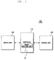
- FIG. 1 is a block diagram illustrating a configuration of a mobile terminal according to an exemplary embodiment of the present invention
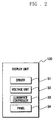
- FIG. 2 is a block diagram illustrating a display unit in the mobile terminal of FIG. 1 .
- a mobile terminal 100 includes a controller 110, storage unit 120, and display unit 130.
- the display unit 130 displays various menu screens of the mobile terminal 100, data input by a user, function setting information, and various information provided to the user.
- the display unit 130 can be operated as an input unit (not shown).
- the display unit 130 is formed as an AMOLED.
- the display unit 130 includes a driver 31, a voltage unit 32, a luminance controller 33, and a panel 34 (see Figure 2 ).
- the panel 34 includes a polarizer, upper glass, lower glass, and an organic material layer positioned between the upper glass and the lower glass(not shown).
- the organic material layer is divided into a plurality of unit areas by a plurality of gate lines and a plurality of data lines intersecting each other.
- Light emitting pixels are mounted in each of the plurality of unit areas.
- Each light emitting pixel includes red (R), green (G), Blue (B) OLEDS.
- the panel 34 controls an amount of light emitted according to the frame data rate by the control of the luminance controller 33. In other words, in the present exemplary embodiment, when the panel 34 displays an image including a large amount of bright color under the control of the luminance controller 33, the amount of light emitted can be reduced.
- a light emitting principle of the OLED light emitting pixel is well known to a person of ordinary skill in the art and therefore a detailed description thereof is omitted.
- the driver 31 drives the light emitting pixels on the panel 34 according to image data received from the controller 110 ( Figure 1 ).
- the driver 31 includes a data driver, gate driver, and timing controller (not shown).
- the gate driver can sequentially enable a plurality of gate lines on the panel 34 in each frame (period of a vertical synchronizing signal) during a predetermined period (for example, a period of a horizontal synchronizing signal).
- the gate driver can operate according to a gate control signal including a clock signal having a gate start pulse and a period of the horizontal synchronizing signal (not shown).
- the data driver supplies an image data signal of a line to a plurality of data lines on the panel 34.
- the data driver inputs image data to the plurality of data lines in a stream form according to a data control signal.
- the timing controller (not shown) controls a driving time of the gate driver and the data driver. That is, the timing controller generates a gate control signal and a data control signal according to a sync signal. Further, the timing controller receives image data of a frame unit from the controller 110, aligns the image data on a data line basis, and supplies the image data to the data driver.
- the voltage unit 32 generates a driving voltage necessary for the light emitting pixels on the panel 34.
- the driving voltage is commonly supplied to the light emitting pixels on the panel 34.
- light emitting pixels on the panel 34 driven by a driving voltage of the voltage unit 32 can be selectively enabled in a line by line manner by the gate driver.
- the enabled light emitting pixels charge to a predetermined voltage according to image data supplied via the data line from the data driver and emit light to correspond to the charged voltage.
- the light emitting pixel outputs a color based on the voltages applied to the pixel elements to display an image.
- the luminance controller 33 controls luminance of a light emitting pixel on the panel 34 under the control of the controller 110.
- the luminance controller 33 controls a voltage or a current supplied to a light emitting pixel on the panel 34.
- the luminance controller 33 receives a luminance control signal from the controller 110 according to a luminance reducing amount mapped to the frame data rate and controls the entire luminance of the display unit 130 to correspond to the luminance control signal. That is, when a bright image having a large power consumption is displayed, the luminance controller 33 reduces a voltage or a current supplied to the light emitting pixel according to the luminance control signal.
- the storage unit 120 stores a program necessary for a function operation and user data according to the present exemplary embodiment.
- the storage unit 120 includes a program area and a data area.
- the program area stores a program for controlling general operations of the mobile terminal 100, an operating system for booting the mobile terminal 100, and an application program necessary for other option functions, for example, a camera function, digital broadcasting reception function, image or moving picture reproducing function, and music reproducing function of the mobile terminal 100.
- the program area includes a program for controlling the entire luminance of the display unit 130 according to the frame data rate.
- the data area is an area for storing data generated according to use of the mobile terminal 100 and stores information corresponding to a phonebook, audio data, related content, or other user data. Particularly, in the present exemplary embodiment, the data area stores a luminance reducing amount according to the frame data rate as is shown in Table 1.
- Table 1 Frame data rate Luminance reducing amount 0 to less than 50% (dark screen) None 50 to less than 70% (intermediate Reduce one step brightness screen) 70 to less than 90% (bright screen) Reduce two steps
- an image is divided into three steps according to a frame data rate of the image data, and a luminance reducing (adjustment) amount changes according to each step. That is, in an image in which an occupying ratio of a bright color is high, a luminance reducing (adjustment) amount increases in order to reduce the current consumption of an image in which an occupying ratio of a bright color is high.
- a luminance reducing (adjustment) amount increases in order to reduce the current consumption of an image in which an occupying ratio of a bright color is high.
- the luminance reducing amount may be changed according to a designer's intention.
- a luminance reducing amount according to the frame data rate provides reduction in the luminance in a step-wise manner, however the luminance reducing amount may be a specific value mapped to the frame data rate.
- the luminance reduction amount (adjustment factor) may be set to a default amount of 10% of the luminance and when the frame data rate is 70 to less than 90%, the luminance reduction amount may be set to a default amount of 30% of luminance.
- the luminance reducing amount can be optimized by a designer through experimentation. This is because a current consumption amount can change according to a size of the panel 34 or a driving voltage.
- the luminance reducing amount is based on a bright color, and when the luminance reducing amount is based on a dark color, the luminance reducing amount can change.
- Table 1 an image according to the frame data rate is divided into three steps, however the image may be subdivided or reduced in a larger number (or finite step size) according to a designer's requirements.
- the controller 110 controls general operations of the mobile terminal 100 and a signal flow between units of the mobile terminal 100 and performs a data processing function.
- the controller 110 includes an image analyzing unit 10 (see Figure 1 ).
- the image analyzing unit 10 determines image data and calculates a frame data rate, which is an occupying ratio of a bright color included in the image data. For this, the image analyzing unit 10 counts R, G, B bits representing color information of the light emitting pixel.
- a light emitting pixel includes R, G, B light-emitting diodes, and the R, G, B light-emitting diodes each have a value of 6 bits and can adjust brightness accordingly. That is, a pixel can be expressed with 18 bits (driving word). For example, when a driving word of the light emitting pixel is '0', i.e.
- the pixel is displayed with a black color
- a driving word is '1', i.e. "111111111111111111”
- the pixel is displayed with a white color.
- the image analyzing unit 10 calculates a frame data rate by counting the light emitting pixel quantity representing a white color of the entire pixel. That is, as a ratio of a light emitting pixel representing a white color increases, and an image having large current consumption is displayed, the display is controlled to lower a voltage or a current value input to the light emitting pixel.
- the image analyzing unit 10 determines a part of upper level bits(for example, upper level 3 bits) of each of R, G, and B light-emitting diodes and calculates a frame data rate. For example, by counting the quantity of light emitting pixels in which upper level 3 bits is 1, i.e. the entire driving word expressed as "111***111***111***", the frame data rate may be calculated.
- the image analyzing unit 10 determines only a part of upper level bits (for example, upper level 9 bits) in the entire driving word and calculates a frame data rate.
- the frame data rate is divided into 3 steps, however the present invention is not limited thereto. That is, in the present invention, the frame data rate can be set to a plurality of steps according to a designer's requirements, without altering the scope of the invention. Further, the frame data rate is calculated by counting a light emitting pixel quantity representing the white color, however the present invention is not limited thereto. For example, the frame data rate can be calculated based on a specific color according to a black color or a designer's intention. When an image is a moving picture, the frame data rate is periodically calculated, and when an image is a still picture, if the image is converted to a different image, the frame data rate is calculated.
- the controller 110 controls luminance of image data according to the frame data rate. In other words, when the frame data rate is large (for example, more than 50%), the controller 110 determines that the display unit 130 consumes a large amount of current and reduces luminance, i.e. brightness of the display unit 130. For this, the controller 110 transmits a luminance control signal to the luminance controller 33.
- the image analyzing unit 10 calculates a frame data rate by determining an entire image data corresponding to a frame, however the present invention is not limited thereto. That is, the image analyzing unit 10 calculates the frame data rate by determining some of image data corresponding to a frame, thereby preventing an overload of the system from being generated.
- a mobile terminal using an AMOLED when displaying an image in which an occupying ratio of a bright color is high, power consumption can be reduced by reducing entire luminance. Furthermore, a battery use time period of a mobile terminal can be increased as less power is being consumed.
- the mobile terminal 100 may include constituent elements having an additional function, such as a camera module for photographing an image or a moving picture, broadcasting reception module for receiving digital broadcasting, audio signal output device such as a speaker, audio signal input device such as a microphone, and digital sound source reproducing module such as an MP3 module.
- constituent elements having an additional function, such as a camera module for photographing an image or a moving picture, broadcasting reception module for receiving digital broadcasting, audio signal output device such as a speaker, audio signal input device such as a microphone, and digital sound source reproducing module such as an MP3 module.
- Such constituent elements are variously added according to a convergence trend of digital appliances and all constituent elements cannot be listed, and constituent elements identical to or corresponding to the above constituent elements can be further included in the mobile terminal 100 according to the present exemplary embodiment.
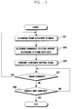
- FIG. 3 is a flowchart illustrating a method of controlling power of an AMOLED according to another exemplary embodiment of the present invention.
- the controller 110 determines a frame data rate of an image to be output (301).
- the frame data rate is an occupying ratio of a bright color included in the image data.
- the frame data rate can be calculated by counting RGB bits representing color information of a light emitting pixel.
- a method of calculating the frame data rate as previously described may include counting a number of high order bits in each color in a pixel.
- the controller 110 determines a luminance reducing amount according to the frame data rate (303).
- the storage unit 120 stores a luminance reducing amount according to the frame data rate in a table form.
- the luminance reducing amount is set to provide a step wise decrease of the luminance value or may further implement a piece-wise linear reduction by determining reduction of the luminance as a percentage of the luminance value, wherein the reduction percentage is different for different range or may be set to a specific value.
- the controller 110 transmits a luminance control signal according to the luminance reducing amount to the luminance controller 33 (305).
- the luminance controller 33 having received the luminance control signal controls the entire luminance of the display unit 130 by adjusting an output current or voltage of the driver 31. For example, when the frame data rate is 80%, the controller 110 transmits a luminance control signal for reducing the luminance by two steps according to Table 1 to the luminance controller 33.
- the luminance reducing amount can be optimized by a designer through experimentation. This is because a current consuming amount changes according to a size of the panel 34 or a driving voltage.
- the luminance controller 33 having received the luminance control signal reduces the entire luminance of the display unit 130 by controlling an output current or voltage of the driver 31.
- the controller 110 determines whether an image changes (307). If an image changes, the process returns to step 301. If an image does not change, the controller 110 determines whether the display unit 130 is turned off (309).
- the above-described methods according to the present invention can be realized in hardware or as software or computer code that can be stored in a recording medium such as a CD ROM, an RAM, a floppy disk, a hard disk, or a magneto-optical disk or downloaded over a network, so that the methods described herein can be executed by such software using a general purpose computer, or a special processor or in programmable or dedicated hardware, such as an ASIC or FPGA.
- the computer, the processor or the programmable hardware include memory components, e.g., RAM, ROM, Flash, etc. that may store or receive software or computer code that when accessed and executed by the computer, processor or hardware implement the processing methods described herein.
- the general purpose computer is transformed into a special purpose computer that may at least perform the processing shown herein.
- the present invention can be applied to both a still picture and a moving picture.
- a load can be applied to a system to control luminance by determining a frame data rate on a frame basis. Therefore, in the present invention, when a moving picture is output, by periodically determining the frame data rate, luminance of the display unit 130 is controlled.
- luminance is controlled by calculating an occupying ratio of a bright color (for example, a white color), however the present invention is not limited thereto. That is, in the present invention, by determining an occupying ratio of a specific color according to a designer's intention, luminance of the display unit 130 is controlled.
- a bright color for example, a white color
- controller 110 determines a reduction factor that is transmitted to the display (step 305) and the display performs the reduction
- controller may determine a reduction factor and alter the luminance value to be output.
- the altered luminance value may then be provided to the display and the display outputs the image based on the altered luminance value. This is advantageous as it allows for the incorporation of the present invention into existing devices.
Description
- The present invention relates to light-emitting diode devices, and more particularly, to a method and device for controlling power of an active matrix organic light-emitting diode.
- A display device of a mobile terminal may be one of a liquid crystal display, field emission display, plasma display panel, and organic light emitting display.
- The organic light emitting display of the display device of the mobile terminal uses an organic light emitting diode (hereinafter, an OLED) that generates light while coupling electrons and holes in an organic material layer when a current flows to a fluorescent or phosphorescent organic thin film. Such an OLED is classified into a passive matrix organic light-emitting diode (a PMOLED) and an active matrix organic light-emitting diode (an AMOLED). The PMOLED uses a line driving method in which an entire line of devices is driven to emit light at one time. The AMOLED uses a method in which each light emitting element is individually driven to emit light. The light emitting element(i.e., pixel) includes a red (R) OLED element for emitting red color light, green (G) OLED element for emitting green color light, and blue (B) OLED element for emitting blue color light. The light emitting element can express a desired color by mixing light of the three colors from the corresponding light emittingelements.
- The AMOLED is widely used in various fields such as a mobile communication terminal, personal digital assistant (PDA), and Moving Picture Experts Group layer-3 (MP3) player due to various advantages such as excellent color reproducibility, thickness, quick response speed, large viewing angle, and high contrast ratio. However, in order to display a bright color, the AMOLED drives all R, G, and B OLEDS and thus when displaying an image (for example, an image including a large quantity of white color) in which an occupying ratio of a bright color is high, power consumption quickly increases.
-
EP 1 622 119 A1 discloses a method and an apparatus for controlling the power level and/or the contrast in a display device having a plurality of luminous elements corresponding to the colour components of the pixels of a picture, wherein the luminance generated by each of said luminous element is based on the intensity of the signal supplied to the luminous element and the power level and/or contrast for each picture is controlled by adjusting the intensity of the signal to be supplied to each luminous element.EP 1 622 119 A1 further discloses applying this to organic light emitting displays (OLED).EP 1 622 119 A1 further discloses the intensity of the signal to be supplied to each luminous element is based on reference signals and the adjustment of the signal intensity is made by adjusting the level of the reference signals.US 2008/088548 A1 discloses an organic light emitting diode display device. The device includes a brightness controller configured to selectively control a brightness controlling range based at least in part on the magnitude of the video data input in one frame, and a gamma correcting unit configured to control the portion of maximum luminance corresponding to full scale data based on one of first gamma correcting values and second gamma correcting values. - The present invention provides a method and device for controlling power of an AMOLED that can reduce power consumption by reducing an entire luminance when displaying an image in which an occupying ratio of a bright color is high.
- The present invention is defined in the independent claims.
- Preferred embodiments are set out in the dependent claims.
- The above features and advantages of the present invention will be more apparent from the following detailed description in conjunction with the accompanying drawings, in which:
-
FIG. 1 is a block diagram illustrating a configuration of a mobile terminal according to an exemplary embodiment of the present invention; -
FIG. 2 is a block diagram illustrating a display unit in the mobile terminal ofFIG. 1 ; and -
FIG. 3 is a flowchart illustrating a method of controlling power of an AMOLED according to an exemplary embodiment of the present invention. - Exemplary embodiments of the present invention are described in detail with reference to the accompanying drawings. The same reference numbers are used throughout the drawings to refer to the same or like parts. Detailed descriptions of well-known functions and structures incorporated herein may be omitted to avoid obscuring the subject matter of the present invention.
- While the present invention may be embodied in many different forms, specific embodiments of the present invention are shown in the drawings and are described herein in detail, with the understanding that the present disclosure is to be considered as an exemplification of the principles of the invention and is not intended to limit the invention to the specific embodiments illustrated.
- In the following description, a mobile terminal according to the present exemplary embodiment may be an information and communication device or a multimedia device such as a mobile phone, PDA, smart phone, International Mobile Telecommunication 2000 (IMT-2000) terminal, code division multiple access (CDMA) terminal, wideband code division multiple access (WCDMA) terminal, Global System for Mobile Communication (GSM) terminal, general packet radio service (GPRS) terminal, universal mobile telecommunication service (UMTS) terminal, digital broadcasting terminal, laptop computer, television, large format display (LFD), navigation terminal , and applications thereof.
- A "frame data rate" is presented as being an occupying ratio of a specific color (for example, a white color) in an image data of a frame.
-
FIG. 1 is a block diagram illustrating a configuration of a mobile terminal according to an exemplary embodiment of the present invention, andFIG. 2 is a block diagram illustrating a display unit in the mobile terminal ofFIG. 1 . - Referring to
FIGS. 1 and2 , amobile terminal 100 includes acontroller 110,storage unit 120, anddisplay unit 130. - The
display unit 130 displays various menu screens of themobile terminal 100, data input by a user, function setting information, and various information provided to the user. When thedisplay unit 130 is formed as a touch screen, thedisplay unit 130 can be operated as an input unit (not shown). Particularly, in the present exemplary embodiment, thedisplay unit 130 is formed as an AMOLED. Thedisplay unit 130 includes adriver 31, avoltage unit 32, aluminance controller 33, and a panel 34 (seeFigure 2 ). - The
panel 34 includes a polarizer, upper glass, lower glass, and an organic material layer positioned between the upper glass and the lower glass(not shown). The organic material layer is divided into a plurality of unit areas by a plurality of gate lines and a plurality of data lines intersecting each other. Light emitting pixels are mounted in each of the plurality of unit areas. Each light emitting pixel includes red (R), green (G), Blue (B) OLEDS. Particularly, in the present exemplary embodiment, thepanel 34 controls an amount of light emitted according to the frame data rate by the control of theluminance controller 33. In other words, in the present exemplary embodiment, when thepanel 34 displays an image including a large amount of bright color under the control of theluminance controller 33, the amount of light emitted can be reduced. - A light emitting principle of the OLED light emitting pixel is well known to a person of ordinary skill in the art and therefore a detailed description thereof is omitted.
- The
driver 31 drives the light emitting pixels on thepanel 34 according to image data received from the controller 110 (Figure 1 ). For this, thedriver 31 includes a data driver, gate driver, and timing controller (not shown). - The gate driver can sequentially enable a plurality of gate lines on the
panel 34 in each frame (period of a vertical synchronizing signal) during a predetermined period (for example, a period of a horizontal synchronizing signal). For this, the gate driver can operate according to a gate control signal including a clock signal having a gate start pulse and a period of the horizontal synchronizing signal (not shown). - Whenever one of a plurality of gate lines is enabled (i.e. in each period of a horizontal synchronizing signal), the data driver supplies an image data signal of a line to a plurality of data lines on the
panel 34. For this, the data driver inputs image data to the plurality of data lines in a stream form according to a data control signal. - The timing controller (not shown) controls a driving time of the gate driver and the data driver. That is, the timing controller generates a gate control signal and a data control signal according to a sync signal. Further, the timing controller receives image data of a frame unit from the
controller 110, aligns the image data on a data line basis, and supplies the image data to the data driver. - The
voltage unit 32 generates a driving voltage necessary for the light emitting pixels on thepanel 34. The driving voltage is commonly supplied to the light emitting pixels on thepanel 34. In this case, light emitting pixels on thepanel 34 driven by a driving voltage of thevoltage unit 32 can be selectively enabled in a line by line manner by the gate driver. The enabled light emitting pixels charge to a predetermined voltage according to image data supplied via the data line from the data driver and emit light to correspond to the charged voltage. Thus, the light emitting pixel outputs a color based on the voltages applied to the pixel elements to display an image. - The
luminance controller 33 controls luminance of a light emitting pixel on thepanel 34 under the control of thecontroller 110. For this, theluminance controller 33 controls a voltage or a current supplied to a light emitting pixel on thepanel 34. Particularly, in the present exemplary embodiment, theluminance controller 33 receives a luminance control signal from thecontroller 110 according to a luminance reducing amount mapped to the frame data rate and controls the entire luminance of thedisplay unit 130 to correspond to the luminance control signal. That is, when a bright image having a large power consumption is displayed, theluminance controller 33 reduces a voltage or a current supplied to the light emitting pixel according to the luminance control signal. - The
storage unit 120 stores a program necessary for a function operation and user data according to the present exemplary embodiment. Thestorage unit 120 includes a program area and a data area. - The program area stores a program for controlling general operations of the
mobile terminal 100, an operating system for booting themobile terminal 100, and an application program necessary for other option functions, for example, a camera function, digital broadcasting reception function, image or moving picture reproducing function, and music reproducing function of themobile terminal 100. Particularly, in the present exemplary embodiment, the program area includes a program for controlling the entire luminance of thedisplay unit 130 according to the frame data rate. - The data area is an area for storing data generated according to use of the
mobile terminal 100 and stores information corresponding to a phonebook, audio data, related content, or other user data. Particularly, in the present exemplary embodiment, the data area stores a luminance reducing amount according to the frame data rate as is shown in Table 1.Table 1 Frame data rate Luminance reducing amount 0 to less than 50% (dark screen) None 50 to less than 70% (intermediate Reduce one step brightness screen) 70 to less than 90% (bright screen) Reduce two steps - In Table 1, in the present exemplary embodiment, an image is divided into three steps according to a frame data rate of the image data, and a luminance reducing (adjustment) amount changes according to each step. That is, in an image in which an occupying ratio of a bright color is high, a luminance reducing (adjustment) amount increases in order to reduce the current consumption of an image in which an occupying ratio of a bright color is high. For example, when the frame data rate is 70% to less than 90%, the luminance is set to a default reduction of two steps, and when the frame data rate is 50% to less than 70%, the luminance is set to a default reduction of one step. As would be recognized, the luminance reducing amount may be changed according to a designer's intention.
- The present invention is not limited to values of Table 1. That is, in Table 1, a luminance reducing amount according to the frame data rate provides reduction in the luminance in a step-wise manner, however the luminance reducing amount may be a specific value mapped to the frame data rate. For example, when the frame data rate is 50 to less than 70%, the luminance reduction amount (adjustment factor) may be set to a default amount of 10% of the luminance and when the frame data rate is 70 to less than 90%, the luminance reduction amount may be set to a default amount of 30% of luminance. The luminance reducing amount can be optimized by a designer through experimentation. This is because a current consumption amount can change according to a size of the
panel 34 or a driving voltage. Further, the luminance reducing amount is based on a bright color, and when the luminance reducing amount is based on a dark color, the luminance reducing amount can change. Further, in Table 1, an image according to the frame data rate is divided into three steps, however the image may be subdivided or reduced in a larger number (or finite step size) according to a designer's requirements. - The
controller 110 controls general operations of themobile terminal 100 and a signal flow between units of themobile terminal 100 and performs a data processing function. Particularly, in the present exemplary embodiment, thecontroller 110 includes an image analyzing unit 10 (seeFigure 1 ). - The
image analyzing unit 10 determines image data and calculates a frame data rate, which is an occupying ratio of a bright color included in the image data. For this, theimage analyzing unit 10 counts R, G, B bits representing color information of the light emitting pixel. In more detail, a light emitting pixel includes R, G, B light-emitting diodes, and the R, G, B light-emitting diodes each have a value of 6 bits and can adjust brightness accordingly. That is, a pixel can be expressed with 18 bits (driving word). For example, when a driving word of the light emitting pixel is '0', i.e. "000000000000000000", the pixel is displayed with a black color, and when a driving word is '1', i.e. "111111111111111111", the pixel is displayed with a white color. When each of the bits of the driving word is a '1', i.e. when a white color is displayed, the largest amount of current is consumed. Therefore, theimage analyzing unit 10 calculates a frame data rate by counting the light emitting pixel quantity representing a white color of the entire pixel. That is, as a ratio of a light emitting pixel representing a white color increases, and an image having large current consumption is displayed, the display is controlled to lower a voltage or a current value input to the light emitting pixel. - In this case, the
image analyzing unit 10 determines a part of upper level bits(for example, upper level 3 bits) of each of R, G, and B light-emitting diodes and calculates a frame data rate. For example, by counting the quantity of light emitting pixels in which upper level 3 bits is 1, i.e. the entire driving word expressed as "111***111***111***", the frame data rate may be calculated. The reason why to determine only a part of upper level bits is that lower level bits represent a minute color change and do not have a great difference in a current consumption aspect. Alternatively, theimage analyzing unit 10 determines only a part of upper level bits (for example, upper level 9 bits) in the entire driving word and calculates a frame data rate. In the present exemplary embodiment, the frame data rate is divided into 3 steps, however the present invention is not limited thereto. That is, in the present invention, the frame data rate can be set to a plurality of steps according to a designer's requirements, without altering the scope of the invention. Further, the frame data rate is calculated by counting a light emitting pixel quantity representing the white color, however the present invention is not limited thereto. For example, the frame data rate can be calculated based on a specific color according to a black color or a designer's intention. When an image is a moving picture, the frame data rate is periodically calculated, and when an image is a still picture, if the image is converted to a different image, the frame data rate is calculated. - The
controller 110 controls luminance of image data according to the frame data rate. In other words, when the frame data rate is large (for example, more than 50%), thecontroller 110 determines that thedisplay unit 130 consumes a large amount of current and reduces luminance, i.e. brightness of thedisplay unit 130. For this, thecontroller 110 transmits a luminance control signal to theluminance controller 33. - In the present exemplary embodiment, the
image analyzing unit 10 calculates a frame data rate by determining an entire image data corresponding to a frame, however the present invention is not limited thereto. That is, theimage analyzing unit 10 calculates the frame data rate by determining some of image data corresponding to a frame, thereby preventing an overload of the system from being generated. - As described above, in the present invention, in a mobile terminal using an AMOLED, when displaying an image in which an occupying ratio of a bright color is high, power consumption can be reduced by reducing entire luminance. Furthermore, a battery use time period of a mobile terminal can be increased as less power is being consumed.
- Further, although not shown, the
mobile terminal 100 may include constituent elements having an additional function, such as a camera module for photographing an image or a moving picture, broadcasting reception module for receiving digital broadcasting, audio signal output device such as a speaker, audio signal input device such as a microphone, and digital sound source reproducing module such as an MP3 module. Such constituent elements are variously added according to a convergence trend of digital appliances and all constituent elements cannot be listed, and constituent elements identical to or corresponding to the above constituent elements can be further included in themobile terminal 100 according to the present exemplary embodiment. - Hereinafter, a method of controlling power of an AMOLED is described.
-
FIG. 3 is a flowchart illustrating a method of controlling power of an AMOLED according to another exemplary embodiment of the present invention. - Referring to
FIGS. 1 to 3 , when an image (including a still picture and a moving picture) output event occurs, thecontroller 110 determines a frame data rate of an image to be output (301). The frame data rate is an occupying ratio of a bright color included in the image data. The frame data rate can be calculated by counting RGB bits representing color information of a light emitting pixel. A method of calculating the frame data rate as previously described may include counting a number of high order bits in each color in a pixel. - The
controller 110 determines a luminance reducing amount according to the frame data rate (303). For this, thestorage unit 120 stores a luminance reducing amount according to the frame data rate in a table form. The luminance reducing amount is set to provide a step wise decrease of the luminance value or may further implement a piece-wise linear reduction by determining reduction of the luminance as a percentage of the luminance value, wherein the reduction percentage is different for different range or may be set to a specific value. - The
controller 110 transmits a luminance control signal according to the luminance reducing amount to the luminance controller 33 (305). Theluminance controller 33, having received the luminance control signal controls the entire luminance of thedisplay unit 130 by adjusting an output current or voltage of thedriver 31. For example, when the frame data rate is 80%, thecontroller 110 transmits a luminance control signal for reducing the luminance by two steps according to Table 1 to theluminance controller 33. The luminance reducing amount can be optimized by a designer through experimentation. This is because a current consuming amount changes according to a size of thepanel 34 or a driving voltage. - The
luminance controller 33, having received the luminance control signal reduces the entire luminance of thedisplay unit 130 by controlling an output current or voltage of thedriver 31. - The
controller 110 determines whether an image changes (307). If an image changes, the process returns to step 301. If an image does not change, thecontroller 110 determines whether thedisplay unit 130 is turned off (309). - If the
display unit 130 is not turned off, the process returns to step 307. If thedisplay unit 130 is turned off, thecontroller 110 terminates the power control process.. - The above-described methods according to the present invention can be realized in hardware or as software or computer code that can be stored in a recording medium such as a CD ROM, an RAM, a floppy disk, a hard disk, or a magneto-optical disk or downloaded over a network, so that the methods described herein can be executed by such software using a general purpose computer, or a special processor or in programmable or dedicated hardware, such as an ASIC or FPGA. As would be understood in the art, the computer, the processor or the programmable hardware include memory components, e.g., RAM, ROM, Flash, etc. that may store or receive software or computer code that when accessed and executed by the computer, processor or hardware implement the processing methods described herein. As would be recognized by those skilled in the art, when a general purpose computer is loaded with, or accesses, software or code for implementing the processing shown herein, the general purpose computer is transformed into a special purpose computer that may at least perform the processing shown herein.
- As described above, the present invention can be applied to both a still picture and a moving picture. When a moving picture is output, a load can be applied to a system to control luminance by determining a frame data rate on a frame basis. Therefore, in the present invention, when a moving picture is output, by periodically determining the frame data rate, luminance of the
display unit 130 is controlled. - In the present exemplary embodiment, luminance is controlled by calculating an occupying ratio of a bright color (for example, a white color), however the present invention is not limited thereto. That is, in the present invention, by determining an occupying ratio of a specific color according to a designer's intention, luminance of the
display unit 130 is controlled. - As described above, in a method and device for controlling power of an AMOLED according to the present invention, when an image in which an occupying ratio of a bright color is high is displayed, power consumption can be reduced and thus a battery use time period of a mobile terminal can be extended.
- Although exemplary embodiments of the present invention have been described in detail hereinabove, it should be clearly understood that many variations and modifications of the basic inventive concepts herein described which fall within the scope of the present invention as defined in the appended claims may appear to those skilled in the art. For example, although it has been described that the
controller 110 determines a reduction factor that is transmitted to the display (step 305) and the display performs the reduction, it would be recognized that the controller may determine a reduction factor and alter the luminance value to be output. The altered luminance value may then be provided to the display and the display outputs the image based on the altered luminance value. This is advantageous as it allows for the incorporation of the present invention into existing devices.
Claims (10)
- A method for controlling power of a mobile terminal comprising a display unit formed with an active matrix organic light-emitting diode (AMOLED), comprising:counting a quantity of pixels of an image to be displayed in which each of the high order bits of R, G and B driving words, indicating color information of each of the pixels, has the same value;calculating a frame data rate, which is a ratio of said counted quantity of pixels to a total quantity of pixels in the image to be displayed with the display unit (301);determining a luminance reducing amount mapped to the frame data rate (303); andcontrolling and displaying an entire luminance of the image according to the luminance reducing amount (305).
- The method of claim 1, wherein calculating a frame data rate is performed whenever an image changes.
- The method of claim 1, wherein controlling and displaying the entire luminance of the image according to the luminance reducing amount (305) comprises adjusting the light emitting amount of the pixels by adjusting at least one of a current and a voltage supplied to the pixels.
- The method of claim 1, wherein controlling and displaying the entire luminance of the image according to the luminance reducing amount (305) comprises reducing the entire luminance of the image in a step-wise manner according to the frame data rate.
- A mobile terminal for controlling power, comprising:a display unit (130) for displaying image and formed with an active matrix organic light-emitting diode (AMOLED); anda controller (110) configured for:counting a quantity of pixels of an image to be displayed in which each of the high order bits of R, G and B driving words, indicating color information of each of the pixels, has the same value;calculating a frame data rate, which is a ratio of said counted quantity of pixels to a total quantity of pixels in the image to be displayed with the display unit; and fordetermining a luminance reducing amount based on the calculated frame data rate;wherein the display unit (130) is configured to display the image according to the luminance reducing amount.
- The mobile terminal of claim 5, wherein the controller (110) comprises an image analyzing unit (10) for calculating the frame data rate.
- The mobile terminal of claim 6, wherein the image analyzing unit (10) calculates the frame data rate by counting the quantity of pixels representing a white color.
- The mobile terminal of claim 5, further comprising a storage unit (120) for storing the luminance reducing amount according to the frame data rate.
- The mobile terminal of claim 5, wherein the display unit (130) comprises a luminance controller (33) for controlling luminance of the display unit (130).
- The mobile terminal of claim 9, wherein the luminance controller (33) is configured to adjust a light emitting amount of pixels by controlling one of an output current and voltage of a driver (31) of the display unit (130).
Applications Claiming Priority (1)
| Application Number | Priority Date | Filing Date | Title |
|---|---|---|---|
| KR1020080137034A KR20100078699A (en) | 2008-12-30 | 2008-12-30 | Apparatus and method for power control of amoled |
Publications (2)
| Publication Number | Publication Date |
|---|---|
| EP2204792A1 EP2204792A1 (en) | 2010-07-07 |
| EP2204792B1 true EP2204792B1 (en) | 2016-11-02 |
Family
ID=42077210
Family Applications (1)
| Application Number | Title | Priority Date | Filing Date |
|---|---|---|---|
| EP09179301.8A Not-in-force EP2204792B1 (en) | 2008-12-30 | 2009-12-15 | Method and device for controlling power of active matrix organic light-emitting diode |
Country Status (5)
| Country | Link |
|---|---|
| US (2) | US8730271B2 (en) |
| EP (1) | EP2204792B1 (en) |
| JP (1) | JP5717962B2 (en) |
| KR (1) | KR20100078699A (en) |
| CN (1) | CN101770747A (en) |
Families Citing this family (19)
| Publication number | Priority date | Publication date | Assignee | Title |
|---|---|---|---|---|
| TWI428878B (en) * | 2010-06-14 | 2014-03-01 | Au Optronics Corp | Display driving method and display |
| JP5610942B2 (en) * | 2010-09-09 | 2014-10-22 | キヤノン株式会社 | Display device |
| TWI436336B (en) * | 2011-08-23 | 2014-05-01 | Au Optronics Corp | Method for controlling organic light emitting diode display displaying images |
| KR101313967B1 (en) * | 2011-10-04 | 2013-10-01 | 엘지전자 주식회사 | Display device and method for controlling thereof |
| CN103092546B (en) * | 2011-10-28 | 2018-03-23 | 中兴通讯股份有限公司 | A kind of display methods and device |
| KR101851577B1 (en) | 2012-09-17 | 2018-04-24 | 삼성전자주식회사 | Methods and devices for controlling operations of organic light-emitting diode display |
| CN105989789B (en) * | 2015-02-17 | 2020-03-03 | 奇景光电股份有限公司 | Method for transmitting data from time schedule controller, time schedule controller and display system |
| CN104933983A (en) * | 2015-07-17 | 2015-09-23 | 京东方科技集团股份有限公司 | Method and system for reducing power consumption of mobile terminal |
| KR102588126B1 (en) | 2016-11-01 | 2023-10-13 | 삼성전자주식회사 | Display driver integrated circuit and display driving system including the same |
| KR101940483B1 (en) * | 2016-11-30 | 2019-04-10 | 아주대학교산학협력단 | Method and Apparatus for Dynamically Controlling Voltage Of AMOLED Display |
| CN107680556B (en) * | 2017-11-03 | 2019-08-02 | 深圳市华星光电半导体显示技术有限公司 | A kind of display power-economizing method, device and display |
| CN108288018B (en) * | 2017-11-30 | 2020-04-10 | 维沃移动通信有限公司 | Display module and mobile terminal |
| WO2020157979A1 (en) * | 2019-02-01 | 2020-08-06 | 株式会社ソニー・インタラクティブエンタテインメント | Head mount display and image display method |
| JP7305179B2 (en) * | 2019-09-24 | 2023-07-10 | 株式会社Joled | CURRENT LIMITING CIRCUIT, DISPLAY DEVICE AND CURRENT LIMITING METHOD |
| US20210142749A1 (en) * | 2019-11-13 | 2021-05-13 | Samsung Electronics Co., Ltd. | Display apparatus and control method thereof |
| CN114830218A (en) | 2020-01-03 | 2022-07-29 | 三星电子株式会社 | Display module and driving method thereof |
| CN111627384B (en) * | 2020-05-14 | 2022-09-09 | 深圳市华星光电半导体显示技术有限公司 | Display picture compensation method and device, electronic equipment and storage medium |
| KR102289926B1 (en) * | 2020-05-25 | 2021-08-19 | 주식회사 사피엔반도체 | Apparatus for controlling brightness of display |
| CN113077758B (en) * | 2021-03-29 | 2023-04-28 | 联想(北京)有限公司 | Control method and device and electronic equipment |
Citations (2)
| Publication number | Priority date | Publication date | Assignee | Title |
|---|---|---|---|---|
| US20070115302A1 (en) * | 2005-11-24 | 2007-05-24 | Jih-Fon Huang | Method and structure for automatic adjusting brightness and display apparatus |
| EP1962272A1 (en) * | 2007-02-23 | 2008-08-27 | Samsung SDI Co., Ltd. | Power reduction driving controller, organic light emitting display including the same, and associated methods |
Family Cites Families (27)
| Publication number | Priority date | Publication date | Assignee | Title |
|---|---|---|---|---|
| JP3883890B2 (en) | 2002-03-20 | 2007-02-21 | 三洋電機株式会社 | Luminance control method and luminance control circuit for organic EL display |
| KR100914201B1 (en) * | 2002-12-30 | 2009-08-27 | 엘지디스플레이 주식회사 | Liquid crystal display device and driving method thereof |
| JP4406372B2 (en) * | 2003-01-08 | 2010-01-27 | 東芝モバイルディスプレイ株式会社 | Display device and control method thereof |
| KR100959780B1 (en) * | 2003-09-08 | 2010-05-27 | 삼성전자주식회사 | Liquid crystal display, apparatus and method for driving thereof |
| JP2005301095A (en) | 2004-04-15 | 2005-10-27 | Semiconductor Energy Lab Co Ltd | Display device |
| EP1622119A1 (en) | 2004-07-29 | 2006-02-01 | Deutsche Thomson-Brandt Gmbh | Method and apparatus for power level control and/or contrast control of a display device |
| JP2006047617A (en) * | 2004-08-04 | 2006-02-16 | Hitachi Displays Ltd | Electroluminescence display device and driving method thereof |
| US8004511B2 (en) * | 2004-12-02 | 2011-08-23 | Sharp Laboratories Of America, Inc. | Systems and methods for distortion-related source light management |
| KR20070108949A (en) * | 2005-03-10 | 2007-11-13 | 마츠시타 덴끼 산교 가부시키가이샤 | Display device, contrast adjusting method and contrast adjusting program |
| US20070008297A1 (en) * | 2005-04-20 | 2007-01-11 | Bassetti Chester F | Method and apparatus for image based power control of drive circuitry of a display pixel |
| KR100707639B1 (en) | 2005-04-28 | 2007-04-13 | 삼성에스디아이 주식회사 | Light Emitting Display and Driving Method Thereof |
| JP4923447B2 (en) * | 2005-06-20 | 2012-04-25 | セイコーエプソン株式会社 | Image signal control device, electro-optical device, electronic apparatus having the same, and display method |
| JP2007148064A (en) | 2005-11-29 | 2007-06-14 | Kyocera Corp | Portable electronic apparatus and control method thereof |
| JP4734679B2 (en) * | 2006-03-14 | 2011-07-27 | 富士フイルム株式会社 | Image processing apparatus, method, and program |
| KR100745982B1 (en) | 2006-06-19 | 2007-08-06 | 삼성전자주식회사 | Image processing apparatus and method for reducing power consumed on self-emitting type display |
| JP2008020769A (en) | 2006-07-14 | 2008-01-31 | Epson Imaging Devices Corp | Display device |
| JP2008039801A (en) * | 2006-08-01 | 2008-02-21 | M & S Fine Tec Kk | Liquid crystal display device and system and method of controlling backlight for liquid crystal display device |
| KR100793542B1 (en) | 2006-10-12 | 2008-01-14 | 삼성에스디아이 주식회사 | Organic electro luminescence display and driving method thereof |
| KR20080035137A (en) * | 2006-10-18 | 2008-04-23 | 삼성전자주식회사 | Apparatus and method for driving self-emission display panel |
| TWI357057B (en) * | 2006-11-14 | 2012-01-21 | Mstar Semiconductor Inc | Method for displaying and processing video data an |
| KR100844775B1 (en) | 2007-02-23 | 2008-07-07 | 삼성에스디아이 주식회사 | Organic light emitting display device |
| CN101271208B (en) | 2007-03-19 | 2010-04-21 | 钰瀚科技股份有限公司 | Dynamic backlight control method of LCD device |
| US7920121B2 (en) * | 2007-04-26 | 2011-04-05 | Vastview Technology Inc. | Driving method of liquid crystal display device having dynamic backlight control unit |
| KR101224459B1 (en) * | 2007-06-28 | 2013-01-22 | 엘지디스플레이 주식회사 | Liquid Crystal Display |
| KR100867104B1 (en) * | 2007-07-27 | 2008-11-06 | 전자부품연구원 | Method and apparatus for controlling brightness of back light |
| US9501963B2 (en) * | 2008-07-18 | 2016-11-22 | Hewlett-Packard Development Company, L.P. | Color profiling of monitors |
| US8373644B2 (en) * | 2008-09-23 | 2013-02-12 | Sharp Kabushiki Kaisha | Backlight luminance control apparatus and video display apparatus |
-
2008
- 2008-12-30 KR KR1020080137034A patent/KR20100078699A/en not_active Application Discontinuation
-
2009
- 2009-12-15 US US12/638,275 patent/US8730271B2/en active Active
- 2009-12-15 EP EP09179301.8A patent/EP2204792B1/en not_active Not-in-force
- 2009-12-25 JP JP2009295462A patent/JP5717962B2/en not_active Expired - Fee Related
- 2009-12-29 CN CN200910265727A patent/CN101770747A/en active Pending
-
2014
- 2014-05-16 US US14/279,813 patent/US9514675B2/en active Active
Patent Citations (2)
| Publication number | Priority date | Publication date | Assignee | Title |
|---|---|---|---|---|
| US20070115302A1 (en) * | 2005-11-24 | 2007-05-24 | Jih-Fon Huang | Method and structure for automatic adjusting brightness and display apparatus |
| EP1962272A1 (en) * | 2007-02-23 | 2008-08-27 | Samsung SDI Co., Ltd. | Power reduction driving controller, organic light emitting display including the same, and associated methods |
Also Published As
| Publication number | Publication date |
|---|---|
| JP2010156974A (en) | 2010-07-15 |
| KR20100078699A (en) | 2010-07-08 |
| US8730271B2 (en) | 2014-05-20 |
| US20140247294A1 (en) | 2014-09-04 |
| US9514675B2 (en) | 2016-12-06 |
| EP2204792A1 (en) | 2010-07-07 |
| CN101770747A (en) | 2010-07-07 |
| JP5717962B2 (en) | 2015-05-13 |
| US20100164937A1 (en) | 2010-07-01 |
Similar Documents
| Publication | Publication Date | Title |
|---|---|---|
| EP2204792B1 (en) | Method and device for controlling power of active matrix organic light-emitting diode | |
| CN110634434B (en) | Driving method and driving device of display panel and display device | |
| US8179391B2 (en) | Mobile display device driving apparatus and method that can reduce power consumption | |
| KR100786509B1 (en) | Organic electro luminescence display and driving method thereof | |
| US8059069B2 (en) | Organic light emitting diode display device and driving method thereof | |
| US20190236997A1 (en) | Display driving method and organic light-emitting display device thereof | |
| US20090115720A1 (en) | Liquid crystal display, liquid crystal display module, and method of driving liquid crystal display | |
| US9275571B2 (en) | Method and system to quickly fade the luminance of an OLED display | |
| US20100013866A1 (en) | Light source device and liquid crystal display unit | |
| US8933866B2 (en) | Active matrix pixel brightness control | |
| US20140292838A1 (en) | Organic light emitting display device and driving method thereof | |
| JP2004294752A (en) | El display device | |
| US20080170030A1 (en) | Image processing apparatus | |
| US20070008254A1 (en) | Driving circuit using pulse width modulation technique for a light emitting device | |
| JP2004279990A (en) | El display device | |
| CA2824661C (en) | Active matrix pixel brightness control | |
| JP4969868B2 (en) | Self-luminous display image display method and image display apparatus | |
| CN107491161B (en) | Energy-saving method and system for display | |
| US20100309099A1 (en) | Display device and driving method thereof | |
| WO2022135034A1 (en) | Frame frequency switching method, apparatus, terminal device, and readable storage medium | |
| CN111681603B (en) | Driving method of display panel | |
| JP5259112B2 (en) | Portable electronic devices | |
| CN111477169A (en) | Brightness control method for display mode switching on O L ED panel | |
| JP5364913B2 (en) | Portable electronic devices | |
| CN114141186A (en) | Display parameter adjusting method and device |
Legal Events
| Date | Code | Title | Description |
|---|---|---|---|
| PUAI | Public reference made under article 153(3) epc to a published international application that has entered the european phase |
Free format text: ORIGINAL CODE: 0009012 |
|
| AK | Designated contracting states |
Kind code of ref document: A1 Designated state(s): AT BE BG CH CY CZ DE DK EE ES FI FR GB GR HR HU IE IS IT LI LT LU LV MC MK MT NL NO PL PT RO SE SI SK SM TR |
|
| AX | Request for extension of the european patent |
Extension state: AL BA RS |
|
| 17P | Request for examination filed |
Effective date: 20110107 |
|
| 17Q | First examination report despatched |
Effective date: 20110726 |
|
| RAP1 | Party data changed (applicant data changed or rights of an application transferred) |
Owner name: SAMSUNG ELECTRONICS CO., LTD. |
|
| GRAP | Despatch of communication of intention to grant a patent |
Free format text: ORIGINAL CODE: EPIDOSNIGR1 |
|
| RIC1 | Information provided on ipc code assigned before grant |
Ipc: G09G 3/32 20060101AFI20160408BHEP Ipc: G09G 5/10 20060101ALN20160408BHEP |
|
| INTG | Intention to grant announced |
Effective date: 20160519 |
|
| GRAS | Grant fee paid |
Free format text: ORIGINAL CODE: EPIDOSNIGR3 |
|
| GRAA | (expected) grant |
Free format text: ORIGINAL CODE: 0009210 |
|
| AK | Designated contracting states |
Kind code of ref document: B1 Designated state(s): AT BE BG CH CY CZ DE DK EE ES FI FR GB GR HR HU IE IS IT LI LT LU LV MC MK MT NL NO PL PT RO SE SI SK SM TR |
|
| REG | Reference to a national code |
Ref country code: GB Ref legal event code: FG4D |
|
| REG | Reference to a national code |
Ref country code: AT Ref legal event code: REF Ref document number: 842539 Country of ref document: AT Kind code of ref document: T Effective date: 20161115 Ref country code: CH Ref legal event code: EP |
|
| REG | Reference to a national code |
Ref country code: IE Ref legal event code: FG4D |
|
| REG | Reference to a national code |
Ref country code: DE Ref legal event code: R096 Ref document number: 602009042054 Country of ref document: DE |
|
| REG | Reference to a national code |
Ref country code: NL Ref legal event code: FP |
|
| PG25 | Lapsed in a contracting state [announced via postgrant information from national office to epo] |
Ref country code: LV Free format text: LAPSE BECAUSE OF FAILURE TO SUBMIT A TRANSLATION OF THE DESCRIPTION OR TO PAY THE FEE WITHIN THE PRESCRIBED TIME-LIMIT Effective date: 20161102 |
|
| REG | Reference to a national code |
Ref country code: LT Ref legal event code: MG4D |
|
| REG | Reference to a national code |
Ref country code: AT Ref legal event code: MK05 Ref document number: 842539 Country of ref document: AT Kind code of ref document: T Effective date: 20161102 |
|
| PG25 | Lapsed in a contracting state [announced via postgrant information from national office to epo] |
Ref country code: NO Free format text: LAPSE BECAUSE OF FAILURE TO SUBMIT A TRANSLATION OF THE DESCRIPTION OR TO PAY THE FEE WITHIN THE PRESCRIBED TIME-LIMIT Effective date: 20170202 Ref country code: GR Free format text: LAPSE BECAUSE OF FAILURE TO SUBMIT A TRANSLATION OF THE DESCRIPTION OR TO PAY THE FEE WITHIN THE PRESCRIBED TIME-LIMIT Effective date: 20170203 Ref country code: LT Free format text: LAPSE BECAUSE OF FAILURE TO SUBMIT A TRANSLATION OF THE DESCRIPTION OR TO PAY THE FEE WITHIN THE PRESCRIBED TIME-LIMIT Effective date: 20161102 Ref country code: SE Free format text: LAPSE BECAUSE OF FAILURE TO SUBMIT A TRANSLATION OF THE DESCRIPTION OR TO PAY THE FEE WITHIN THE PRESCRIBED TIME-LIMIT Effective date: 20161102 |
|
| PG25 | Lapsed in a contracting state [announced via postgrant information from national office to epo] |
Ref country code: BE Free format text: LAPSE BECAUSE OF NON-PAYMENT OF DUE FEES Effective date: 20161231 Ref country code: IS Free format text: LAPSE BECAUSE OF FAILURE TO SUBMIT A TRANSLATION OF THE DESCRIPTION OR TO PAY THE FEE WITHIN THE PRESCRIBED TIME-LIMIT Effective date: 20170302 Ref country code: AT Free format text: LAPSE BECAUSE OF FAILURE TO SUBMIT A TRANSLATION OF THE DESCRIPTION OR TO PAY THE FEE WITHIN THE PRESCRIBED TIME-LIMIT Effective date: 20161102 Ref country code: PL Free format text: LAPSE BECAUSE OF FAILURE TO SUBMIT A TRANSLATION OF THE DESCRIPTION OR TO PAY THE FEE WITHIN THE PRESCRIBED TIME-LIMIT Effective date: 20161102 Ref country code: ES Free format text: LAPSE BECAUSE OF FAILURE TO SUBMIT A TRANSLATION OF THE DESCRIPTION OR TO PAY THE FEE WITHIN THE PRESCRIBED TIME-LIMIT Effective date: 20161102 Ref country code: FI Free format text: LAPSE BECAUSE OF FAILURE TO SUBMIT A TRANSLATION OF THE DESCRIPTION OR TO PAY THE FEE WITHIN THE PRESCRIBED TIME-LIMIT Effective date: 20161102 Ref country code: PT Free format text: LAPSE BECAUSE OF FAILURE TO SUBMIT A TRANSLATION OF THE DESCRIPTION OR TO PAY THE FEE WITHIN THE PRESCRIBED TIME-LIMIT Effective date: 20170302 Ref country code: HR Free format text: LAPSE BECAUSE OF FAILURE TO SUBMIT A TRANSLATION OF THE DESCRIPTION OR TO PAY THE FEE WITHIN THE PRESCRIBED TIME-LIMIT Effective date: 20161102 |
|
| PG25 | Lapsed in a contracting state [announced via postgrant information from national office to epo] |
Ref country code: EE Free format text: LAPSE BECAUSE OF FAILURE TO SUBMIT A TRANSLATION OF THE DESCRIPTION OR TO PAY THE FEE WITHIN THE PRESCRIBED TIME-LIMIT Effective date: 20161102 Ref country code: RO Free format text: LAPSE BECAUSE OF FAILURE TO SUBMIT A TRANSLATION OF THE DESCRIPTION OR TO PAY THE FEE WITHIN THE PRESCRIBED TIME-LIMIT Effective date: 20161102 Ref country code: SK Free format text: LAPSE BECAUSE OF FAILURE TO SUBMIT A TRANSLATION OF THE DESCRIPTION OR TO PAY THE FEE WITHIN THE PRESCRIBED TIME-LIMIT Effective date: 20161102 Ref country code: DK Free format text: LAPSE BECAUSE OF FAILURE TO SUBMIT A TRANSLATION OF THE DESCRIPTION OR TO PAY THE FEE WITHIN THE PRESCRIBED TIME-LIMIT Effective date: 20161102 Ref country code: CZ Free format text: LAPSE BECAUSE OF FAILURE TO SUBMIT A TRANSLATION OF THE DESCRIPTION OR TO PAY THE FEE WITHIN THE PRESCRIBED TIME-LIMIT Effective date: 20161102 |
|
| REG | Reference to a national code |
Ref country code: CH Ref legal event code: PL |
|
| REG | Reference to a national code |
Ref country code: DE Ref legal event code: R097 Ref document number: 602009042054 Country of ref document: DE |
|
| PG25 | Lapsed in a contracting state [announced via postgrant information from national office to epo] |
Ref country code: SM Free format text: LAPSE BECAUSE OF FAILURE TO SUBMIT A TRANSLATION OF THE DESCRIPTION OR TO PAY THE FEE WITHIN THE PRESCRIBED TIME-LIMIT Effective date: 20161102 Ref country code: IT Free format text: LAPSE BECAUSE OF FAILURE TO SUBMIT A TRANSLATION OF THE DESCRIPTION OR TO PAY THE FEE WITHIN THE PRESCRIBED TIME-LIMIT Effective date: 20161102 Ref country code: BG Free format text: LAPSE BECAUSE OF FAILURE TO SUBMIT A TRANSLATION OF THE DESCRIPTION OR TO PAY THE FEE WITHIN THE PRESCRIBED TIME-LIMIT Effective date: 20170202 Ref country code: BE Free format text: LAPSE BECAUSE OF FAILURE TO SUBMIT A TRANSLATION OF THE DESCRIPTION OR TO PAY THE FEE WITHIN THE PRESCRIBED TIME-LIMIT Effective date: 20161102 |
|
| PLBE | No opposition filed within time limit |
Free format text: ORIGINAL CODE: 0009261 |
|
| STAA | Information on the status of an ep patent application or granted ep patent |
Free format text: STATUS: NO OPPOSITION FILED WITHIN TIME LIMIT |
|
| PG25 | Lapsed in a contracting state [announced via postgrant information from national office to epo] |
Ref country code: MC Free format text: LAPSE BECAUSE OF FAILURE TO SUBMIT A TRANSLATION OF THE DESCRIPTION OR TO PAY THE FEE WITHIN THE PRESCRIBED TIME-LIMIT Effective date: 20161102 |
|
| REG | Reference to a national code |
Ref country code: FR Ref legal event code: ST Effective date: 20170831 |
|
| REG | Reference to a national code |
Ref country code: IE Ref legal event code: MM4A |
|
| 26N | No opposition filed |
Effective date: 20170803 |
|
| GBPC | Gb: european patent ceased through non-payment of renewal fee |
Effective date: 20170202 |
|
| PG25 | Lapsed in a contracting state [announced via postgrant information from national office to epo] |
Ref country code: LI Free format text: LAPSE BECAUSE OF NON-PAYMENT OF DUE FEES Effective date: 20161231 Ref country code: CH Free format text: LAPSE BECAUSE OF NON-PAYMENT OF DUE FEES Effective date: 20161231 Ref country code: LU Free format text: LAPSE BECAUSE OF NON-PAYMENT OF DUE FEES Effective date: 20161215 Ref country code: FR Free format text: LAPSE BECAUSE OF NON-PAYMENT OF DUE FEES Effective date: 20170102 |
|
| PG25 | Lapsed in a contracting state [announced via postgrant information from national office to epo] |
Ref country code: SI Free format text: LAPSE BECAUSE OF FAILURE TO SUBMIT A TRANSLATION OF THE DESCRIPTION OR TO PAY THE FEE WITHIN THE PRESCRIBED TIME-LIMIT Effective date: 20161102 Ref country code: IE Free format text: LAPSE BECAUSE OF NON-PAYMENT OF DUE FEES Effective date: 20161215 |
|
| PGFP | Annual fee paid to national office [announced via postgrant information from national office to epo] |
Ref country code: DE Payment date: 20171121 Year of fee payment: 9 Ref country code: NL Payment date: 20171121 Year of fee payment: 9 |
|
| PG25 | Lapsed in a contracting state [announced via postgrant information from national office to epo] |
Ref country code: GB Free format text: LAPSE BECAUSE OF NON-PAYMENT OF DUE FEES Effective date: 20170202 |
|
| PG25 | Lapsed in a contracting state [announced via postgrant information from national office to epo] |
Ref country code: HU Free format text: LAPSE BECAUSE OF FAILURE TO SUBMIT A TRANSLATION OF THE DESCRIPTION OR TO PAY THE FEE WITHIN THE PRESCRIBED TIME-LIMIT; INVALID AB INITIO Effective date: 20091215 Ref country code: CY Free format text: LAPSE BECAUSE OF FAILURE TO SUBMIT A TRANSLATION OF THE DESCRIPTION OR TO PAY THE FEE WITHIN THE PRESCRIBED TIME-LIMIT Effective date: 20161102 |
|
| PG25 | Lapsed in a contracting state [announced via postgrant information from national office to epo] |
Ref country code: TR Free format text: LAPSE BECAUSE OF FAILURE TO SUBMIT A TRANSLATION OF THE DESCRIPTION OR TO PAY THE FEE WITHIN THE PRESCRIBED TIME-LIMIT Effective date: 20161102 Ref country code: MK Free format text: LAPSE BECAUSE OF FAILURE TO SUBMIT A TRANSLATION OF THE DESCRIPTION OR TO PAY THE FEE WITHIN THE PRESCRIBED TIME-LIMIT Effective date: 20161102 |
|
| PG25 | Lapsed in a contracting state [announced via postgrant information from national office to epo] |
Ref country code: MT Free format text: LAPSE BECAUSE OF NON-PAYMENT OF DUE FEES Effective date: 20161215 |
|
| REG | Reference to a national code |
Ref country code: DE Ref legal event code: R119 Ref document number: 602009042054 Country of ref document: DE |
|
| REG | Reference to a national code |
Ref country code: NL Ref legal event code: MM Effective date: 20190101 |
|
| PG25 | Lapsed in a contracting state [announced via postgrant information from national office to epo] |
Ref country code: NL Free format text: LAPSE BECAUSE OF NON-PAYMENT OF DUE FEES Effective date: 20190101 |
|
| PG25 | Lapsed in a contracting state [announced via postgrant information from national office to epo] |
Ref country code: DE Free format text: LAPSE BECAUSE OF NON-PAYMENT OF DUE FEES Effective date: 20190702 |