EP2083214A1 - Light emitting diode lamp - Google Patents
Light emitting diode lamp Download PDFInfo
- Publication number
- EP2083214A1 EP2083214A1 EP08153024A EP08153024A EP2083214A1 EP 2083214 A1 EP2083214 A1 EP 2083214A1 EP 08153024 A EP08153024 A EP 08153024A EP 08153024 A EP08153024 A EP 08153024A EP 2083214 A1 EP2083214 A1 EP 2083214A1
- Authority
- EP
- European Patent Office
- Prior art keywords
- light emitting
- heat dissipating
- emitting diode
- fin
- heat
- Prior art date
- Legal status (The legal status is an assumption and is not a legal conclusion. Google has not performed a legal analysis and makes no representation as to the accuracy of the status listed.)
- Granted
Links
Images


Classifications
-
- F—MECHANICAL ENGINEERING; LIGHTING; HEATING; WEAPONS; BLASTING
- F21—LIGHTING
- F21V—FUNCTIONAL FEATURES OR DETAILS OF LIGHTING DEVICES OR SYSTEMS THEREOF; STRUCTURAL COMBINATIONS OF LIGHTING DEVICES WITH OTHER ARTICLES, NOT OTHERWISE PROVIDED FOR
- F21V29/00—Protecting lighting devices from thermal damage; Cooling or heating arrangements specially adapted for lighting devices or systems
- F21V29/50—Cooling arrangements
- F21V29/70—Cooling arrangements characterised by passive heat-dissipating elements, e.g. heat-sinks
- F21V29/74—Cooling arrangements characterised by passive heat-dissipating elements, e.g. heat-sinks with fins or blades
-
- F—MECHANICAL ENGINEERING; LIGHTING; HEATING; WEAPONS; BLASTING
- F21—LIGHTING
- F21K—NON-ELECTRIC LIGHT SOURCES USING LUMINESCENCE; LIGHT SOURCES USING ELECTROCHEMILUMINESCENCE; LIGHT SOURCES USING CHARGES OF COMBUSTIBLE MATERIAL; LIGHT SOURCES USING SEMICONDUCTOR DEVICES AS LIGHT-GENERATING ELEMENTS; LIGHT SOURCES NOT OTHERWISE PROVIDED FOR
- F21K9/00—Light sources using semiconductor devices as light-generating elements, e.g. using light-emitting diodes [LED] or lasers
- F21K9/20—Light sources comprising attachment means
- F21K9/23—Retrofit light sources for lighting devices with a single fitting for each light source, e.g. for substitution of incandescent lamps with bayonet or threaded fittings
-
- F—MECHANICAL ENGINEERING; LIGHTING; HEATING; WEAPONS; BLASTING
- F21—LIGHTING
- F21V—FUNCTIONAL FEATURES OR DETAILS OF LIGHTING DEVICES OR SYSTEMS THEREOF; STRUCTURAL COMBINATIONS OF LIGHTING DEVICES WITH OTHER ARTICLES, NOT OTHERWISE PROVIDED FOR
- F21V23/00—Arrangement of electric circuit elements in or on lighting devices
- F21V23/003—Arrangement of electric circuit elements in or on lighting devices the elements being electronics drivers or controllers for operating the light source, e.g. for a LED array
- F21V23/004—Arrangement of electric circuit elements in or on lighting devices the elements being electronics drivers or controllers for operating the light source, e.g. for a LED array arranged on a substrate, e.g. a printed circuit board
- F21V23/006—Arrangement of electric circuit elements in or on lighting devices the elements being electronics drivers or controllers for operating the light source, e.g. for a LED array arranged on a substrate, e.g. a printed circuit board the substrate being distinct from the light source holder
-
- F—MECHANICAL ENGINEERING; LIGHTING; HEATING; WEAPONS; BLASTING
- F21—LIGHTING
- F21V—FUNCTIONAL FEATURES OR DETAILS OF LIGHTING DEVICES OR SYSTEMS THEREOF; STRUCTURAL COMBINATIONS OF LIGHTING DEVICES WITH OTHER ARTICLES, NOT OTHERWISE PROVIDED FOR
- F21V29/00—Protecting lighting devices from thermal damage; Cooling or heating arrangements specially adapted for lighting devices or systems
- F21V29/50—Cooling arrangements
- F21V29/70—Cooling arrangements characterised by passive heat-dissipating elements, e.g. heat-sinks
- F21V29/74—Cooling arrangements characterised by passive heat-dissipating elements, e.g. heat-sinks with fins or blades
- F21V29/77—Cooling arrangements characterised by passive heat-dissipating elements, e.g. heat-sinks with fins or blades with essentially identical diverging planar fins or blades, e.g. with fan-like or star-like cross-section
- F21V29/773—Cooling arrangements characterised by passive heat-dissipating elements, e.g. heat-sinks with fins or blades with essentially identical diverging planar fins or blades, e.g. with fan-like or star-like cross-section the planes containing the fins or blades having the direction of the light emitting axis
-
- F—MECHANICAL ENGINEERING; LIGHTING; HEATING; WEAPONS; BLASTING
- F21—LIGHTING
- F21V—FUNCTIONAL FEATURES OR DETAILS OF LIGHTING DEVICES OR SYSTEMS THEREOF; STRUCTURAL COMBINATIONS OF LIGHTING DEVICES WITH OTHER ARTICLES, NOT OTHERWISE PROVIDED FOR
- F21V29/00—Protecting lighting devices from thermal damage; Cooling or heating arrangements specially adapted for lighting devices or systems
- F21V29/50—Cooling arrangements
- F21V29/70—Cooling arrangements characterised by passive heat-dissipating elements, e.g. heat-sinks
- F21V29/83—Cooling arrangements characterised by passive heat-dissipating elements, e.g. heat-sinks the elements having apertures, ducts or channels, e.g. heat radiation holes
-
- F—MECHANICAL ENGINEERING; LIGHTING; HEATING; WEAPONS; BLASTING
- F21—LIGHTING
- F21V—FUNCTIONAL FEATURES OR DETAILS OF LIGHTING DEVICES OR SYSTEMS THEREOF; STRUCTURAL COMBINATIONS OF LIGHTING DEVICES WITH OTHER ARTICLES, NOT OTHERWISE PROVIDED FOR
- F21V29/00—Protecting lighting devices from thermal damage; Cooling or heating arrangements specially adapted for lighting devices or systems
- F21V29/85—Protecting lighting devices from thermal damage; Cooling or heating arrangements specially adapted for lighting devices or systems characterised by the material
- F21V29/89—Metals
-
- F—MECHANICAL ENGINEERING; LIGHTING; HEATING; WEAPONS; BLASTING
- F21—LIGHTING
- F21Y—INDEXING SCHEME ASSOCIATED WITH SUBCLASSES F21K, F21L, F21S and F21V, RELATING TO THE FORM OR THE KIND OF THE LIGHT SOURCES OR OF THE COLOUR OF THE LIGHT EMITTED
- F21Y2115/00—Light-generating elements of semiconductor light sources
- F21Y2115/10—Light-emitting diodes [LED]
Definitions
- the invention generally relates to a light emitting diode lamp, especially to a light emitting diode lamp which meets the MR-16 specification and effectively dissipates the heat from the light emitting diode lamp
- the light emitting diode units have been applied to the illumination field.
- the light emitting diode units have been used in traffic lights, flashlights and lamps.
- a conventional light emitting diode lamp is usually disposed with a heat sink to dissipate the heat from the light emitting diode unit.
- the heat sink is mounted to a plurality of heat dissipating fins by soldering.
- the heat dissipating fins are made of thermally conductive metal, especially aluminum which is featured as light weight and good heat dissipating performance. Therefore, the heat sink with soldered heat dissipating fins has been widely used.
- the aluminum fins must be coated with chemical nickel before soldering, which increases the production cost, with more complicate production and longer work hours.
- An object of the invention is to provide a light emitting diode lamp which is made more economically and efficiently dissipates the heat from the light emitting diode lamp.
- the light emitting diode lamp of the invention includes:
- the invention provides the following advantages. Riveting the heat dissipating fins with the substrate together helps the heat dissipating fins be secured by means of urging the opposite sidewall surfaces of each extending arm against the opposite surfaces of each heat dissipating fin. In addition, there is no need of soldering nickel on the heat dissipating fins and no solder is needed as well. Therefore, the production cost and shortened labor hours can be reduced, while loss of heat conduction can be avoided.
- a light emitting diode lamp includes a heat sink 10, a socket 20, a light emitting module 30, a holder 40, a lens 50 and a protection ring 60.
- the heat sink 10 includes a substrate 11 and a plurality of heat dissipating fins 12.
- the substrate 11 includes a base 111 and a plurality of extending arms 112.
- the base 111 can be a round plate or a polygonal plate, for example. In the embodiment as shown, the base 111 is a round plate.
- the base 111 has a top 1111, a bottom 1112 (as shown in FIG. 2 ), side walls 1113, and trough holes 1114 penetrating through the top 1111 and the bottom 1112.
- the extending arms 112 are positioned at intervals from the side walls 1113 of the base 111.
- a slot 113 is formed between two neighboring extending arms 112.
- Each heat dissipating fin 12 can be polygonal plate or a round plate (not shown).
- Each heat dissipating fin 12 has a fin top 121 and a fin bottom 122 opposite to the fin top 121, and has opposite surfaces 123.
- the fin bottoms 122 of the heat dissipating fins 12 respectively extend in a downward slant direction to form corresponding insertion parts 124 (as shown in FIG. 5 ).
- a plurality of recesses 125 are formed on the base 111 of the substrate 11 close to the fin top.
- Each heat dissipating fin 12 is inserted into the corresponding slot 113.
- One of opposite sidewall surfaces 1121 of each extending arm 112 is against one of opposite surfaces 123 of each heat dissipating fin 12 in a manner to secure each heat dissipating fin 12.
- the fin top 121 and the fin bottom 122 of each heat dissipating fin 12 respectively stretch out of the top and the bottom of the substrate 11 in a manner to arrange the heat dissipating fins 12 in circle around the substrate 11, as shown in FIG. 1 .
- the heat dissipating fins 12 and the substrate I form an accommodation space 13 as shown in FIG. 1 .
- each heat dissipating fin 12 is riveted with the substrate 11 so that the combination of the heat dissipating fin 12 and the substrate 11 is pressed down against each extending arm 112 and therefore against the surface 123 of the corresponding heat dissipating fin 12.
- the riveting can be achieved by forcing a plurality of knife edges face-to-face against onto a top and a bottom of the corresponding extending arm 112 until the extending arm 112 is resiliently deformed.
- the sidewall surfaces 1121 of each extending arm 112 thereby are forced against the surface 123 of the corresponding heat dissipating fin 12.
- the socket 20 is a hollow casing which has two holes 21 at its bottom as shown in FIG. 2 and a plurality of inserting sockets 22 as shown in FIG. 1 .
- the insertion parts 124 of the fin bottoms 122 of the heat dissipating fins 12 are respectively inserted into the corresponding inserting sockets 22 as shown in FIG. 5 , so that the socket 20 is firmly fixed at the fin bottoms 122 of the heat dissipating fins 12.
- the light emitting module 30 includes a heat conductor 31, at least one light emitting diode unit 33, a circuit board 34 and two pins 35,
- the heat conductor 31 is attached on the top of the heat sink 10 of the substrate 11.
- a heat dissipating media such as a heat dissipating paste can be further applied between the heat conductor 31 and the substrate 11 to further enhance the heat dissipation.
- the heat conductor 31 is electrically connected to leads 32 which respectively correspond to the through holes 1114 of the base 11, as shown in FIG. 1 .
- the light emitting diode unit 33 is disposed on the heat conductor 31 through which the heat generated by the light emitting diode unit 33 is conducted to the substrate 11 and the heat dissipating fins 12. Air circulated among these heat dissipating fins 12 cools down the heat.
- a gel such as epoxy resin can be filled between the light emitting diode unit 33 and the heat conductor 31 to prevent any short circuit.
- the circuit board 34 has wire routing for voltage conversion.
- the circuit board 34 has two fixtures 36 as shown in FIG. 1 .
- the two leads 32 of the heat conductor 31 penetrate through the through holes 1114 of the base 111 to reach the corresponding fixtures 36 as shown in FIG. 5 .
- the circuit board 34 is electrically connected to the light emitting diode unit 33 on the heat conductor 31.
- the circuit board 34 in this embodiment can be received inside the socket 20.
- the location of the circuit board 34 is not limited to inside the socket 20.
- the circuit board 34 can be located in the accommodation space 13 of the heat sink 10 and electrically connected to the light emitting diode unit 33 in other manner.
- a gel can be filled between the circuit board 34 and the socket 20 to prevent the circuit board 34 from being damaged and wet.
- the pins 35 are electrically connected to the circuit board 34, and penetrate through the holes 21 of the heat set 20.
- the circuit board 34 and the pins 35 comply with the requirements of MR-16 specification.
- the pins 35 are used to connect the circuit to an external power socket.
- the circuit board 34 converts the external power so as to provide the power needed for the light emitting diode unit 33.
- the holder 40 can be a hollow casing which has two pressing arms 41 as shown in FIG. 2 .
- the pressing arm 41 push the top of the heat conductor 31 to be against the top of the substrate 11 in order to further confirm the heat conducting path.
- the holder 40 is received in the accommodation space 13 opposite to the socket 20.
- the holder 40 has a plurality of engaging parts 42 along its periphery.
- the engaging parts 42 are of tapering shape which taper from its top toward its bottom and thus have slant sides.
- the engaging parts 42 of the holder 40 respectively engage with corresponding recesses 125 of the heat dissipating fins 12 so that the heat dissipating fins 12 are secured to the holder 40.
- the fin tops 121 are resiliently deformed by the slant sides of the engaging parts 42. After the engaging parts 42 enter into the corresponding recesses 125, the fin tops 121 returns to its original positions.
- a gel such as epoxy resin can be filled between the holder 40 and the heat dissipating fins 12 to enhance the bonding between the holder 40 and the heat dissipating fins 12 and offer water-proof effect.
- the lens 50 can be made of transparent material, with a thickness reducing from its center to its periphery.
- the lens 50 is positioned inside the holder 40, above the light emitting diode unit 33 so that the light beams from the light emitting diode unit 33 can be efficiently transmitted to a wide range.
- the protection ring 60 is a hollow ring having a plurality of grooves 61 at its bottom to receive corresponding fin tops 121 of the heat dissipating fins 12. The protection ring 60 thereby sleeves the heat dissipating fins 12 from the top of the heat dissipating fins 12.
- Each heat dissipating fin 12 can be further formed with a filling groove 126 on the fin top 121 thereof as shown in FIG. 5 .
- the filling groove 126 is filled with the gel.
- the protection ring 60 is adhered onto the fin tops 121 of the heat dissipating fins 12 to enhance the binding between the protection ring 60 and the heat dissipating fins 12 and prevent the heat dissipating fins 12 from being shifted.
- the user may directly hold the protection ring 60 if the light emitting diode unit needs to be replaced or installed.
- the slot 113 of each extending arm 112 is used to receive the heat dissipating fin 12.
- the heat dissipating fin 12 can be firmly secured.
- the light emitting diode lamp according the invention can be achieved with flowered production cost, less labor hours and simplified production procedure, while without using the electrically nickel plating.
- the light emitting diode lamp according to the invention does not use solders which helps prevent any loss in thermal conduction. Failure of using lead-containing or no-lead solders which either contain lead or contribute to environmental protection. In addition, configures of the heat dissipating fins have improved heat dissipating performance.
Abstract
Description
- The invention generally relates to a light emitting diode lamp, especially to a light emitting diode lamp which meets the MR-16 specification and effectively dissipates the heat from the light emitting diode lamp
- As the progress of the technology development, the light emitting diode units have been applied to the illumination field. In addition, because of its small volume, low power consumption and long service life, the light emitting diode units have been used in traffic lights, flashlights and lamps.
- A conventional light emitting diode lamp is usually disposed with a heat sink to dissipate the heat from the light emitting diode unit. The heat sink is mounted to a plurality of heat dissipating fins by soldering. The heat dissipating fins are made of thermally conductive metal, especially aluminum which is featured as light weight and good heat dissipating performance. Therefore, the heat sink with soldered heat dissipating fins has been widely used.
- However, the aluminum fins must be coated with chemical nickel before soldering, which increases the production cost, with more complicate production and longer work hours.
- Furthermore, since the heat dissipating fins must be soldered, loss in heat conduction occurs due to the difference of heat conduction coefficient between the solder and the heat dissipating fins, resulting in poor heat dissipation.
- Therefore, there is a need of a heat sink which can overcome the above problems.
- An object of the invention is to provide a light emitting diode lamp which is made more economically and efficiently dissipates the heat from the light emitting diode lamp.
- In order to achieve the above and other objectives, the light emitting diode lamp of the invention includes:
- a heat sink, comprising a substrate and a plurality of extending arms, a slot being formed between two neighboring extending arms ; and
- a plurality of heat dissipating fins, inserted into the corresponding slots, one of opposite sidewall surfaces of each extending arm being against one of opposite surfaces of each heat dissipating fin, each heat dissipating fin has a fin top and a fin bottom respectively protruding from a top and a bottom of the substrate, the heat dissipating fin and the top of the substrate forming an accommodation space;
- a socket, firmly fixed at the fin bottoms of the heat dissipating fins;
- a light emitting module, comprising:
- a heat conductor, mounted on the substrate of the heat sink;
- at least one light emitting diode unit, mounted on the heat conductor;
- a circuit board, electrically connected to the light emitting module; and
- two pins, electrically connected to the circuit board, wherein the two pins penetrate through the socket;
- a holder, inside the accommodation space opposite to the socket, and the heat dissipating fins are secured to the holder; and
- a lens, positioned above the light emitting diode unit and assembled inside the holder.
- The invention provides the following advantages. Riveting the heat dissipating fins with the substrate together helps the heat dissipating fins be secured by means of urging the opposite sidewall surfaces of each extending arm against the opposite surfaces of each heat dissipating fin. In addition, there is no need of soldering nickel on the heat dissipating fins and no solder is needed as well. Therefore, the production cost and shortened labor hours can be reduced, while loss of heat conduction can be avoided.
- To provide a further understanding of the invention, the following detailed description illustrates embodiments and examples of the invention, this detailed description being provided only for illustration of the invention.
-
-
FIG. 1 is an exploded view of a light emitting diode lamp according to one embodiment of the invention; -
FIG. 2 is an exploded view of a light emitting diode lamp from another angle of view according to one embodiment of the invention; -
FIG. 3 is a perspective view of a light emitting diode lamp according to one embodiment of the invention; -
FIG. 4 is a perspective view of a light emitting diode from another angle of view according to one embodiment of the invention; -
FIG. 5 is a cross-sectional view of a light emitting diode lamp according to one embodiment of the invention; -
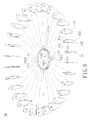
FIG. 6 is an exploded view of a heat sink of a light emitting diode lamp according to one embodiment; and -
FIG. 7 is a schematic view of knife edges forced face-to-face against onto the corresponding extending arm until the extending arm is resiliently deformed according to one embodiment of the invention. - Wherever possible in the following description, like reference numerals will refer to like elements and parts unless otherwise illustrated.
- Referring to
FIG. 1 through FIG. 5 , a light emitting diode lamp according to one embodiment of the invention includes aheat sink 10, asocket 20, alight emitting module 30, aholder 40, alens 50 and aprotection ring 60. - Referring to
FIG. 6 , theheat sink 10 includes asubstrate 11 and a plurality ofheat dissipating fins 12. Thesubstrate 11 includes a base 111 and a plurality of extendingarms 112. The base 111 can be a round plate or a polygonal plate, for example. In the embodiment as shown, the base 111 is a round plate. The base 111 has a top 1111, a bottom 1112 (as shown inFIG. 2 ),side walls 1113, andtrough holes 1114 penetrating through the top 1111 and thebottom 1112. - The extending
arms 112 are positioned at intervals from theside walls 1113 of the base 111. Aslot 113 is formed between two neighboring extendingarms 112. - Each
heat dissipating fin 12 can be polygonal plate or a round plate (not shown). Eachheat dissipating fin 12 has afin top 121 and afin bottom 122 opposite to thefin top 121, and hasopposite surfaces 123. Thefin bottoms 122 of theheat dissipating fins 12 respectively extend in a downward slant direction to form corresponding insertion parts 124 (as shown inFIG. 5 ). A plurality ofrecesses 125 are formed on the base 111 of thesubstrate 11 close to the fin top. - Each
heat dissipating fin 12 is inserted into thecorresponding slot 113. One ofopposite sidewall surfaces 1121 of each extendingarm 112 is against one ofopposite surfaces 123 of each heat dissipating fin 12 in a manner to secure eachheat dissipating fin 12. Thefin top 121 and thefin bottom 122 of eachheat dissipating fin 12 respectively stretch out of the top and the bottom of thesubstrate 11 in a manner to arrange the heat dissipating fins 12 in circle around thesubstrate 11, as shown inFIG. 1 . Theheat dissipating fins 12 and the substrate I form an accommodation space 13 as shown inFIG. 1 . - In this embodiment, each
heat dissipating fin 12 is riveted with thesubstrate 11 so that the combination of theheat dissipating fin 12 and thesubstrate 11 is pressed down against each extendingarm 112 and therefore against thesurface 123 of the correspondingheat dissipating fin 12. - Referring to
FIG. 7 , the riveting can be achieved by forcing a plurality of knife edges face-to-face against onto a top and a bottom of the corresponding extendingarm 112 until the extendingarm 112 is resiliently deformed. Thesidewall surfaces 1121 of each extendingarm 112 thereby are forced against thesurface 123 of the correspondingheat dissipating fin 12. - The
socket 20 is a hollow casing which has twoholes 21 at its bottom as shown inFIG. 2 and a plurality ofinserting sockets 22 as shown inFIG. 1 . Theinsertion parts 124 of thefin bottoms 122 of theheat dissipating fins 12 are respectively inserted into the correspondinginserting sockets 22 as shown inFIG. 5 , so that thesocket 20 is firmly fixed at thefin bottoms 122 of theheat dissipating fins 12. - The
light emitting module 30 includes aheat conductor 31, at least one lightemitting diode unit 33, acircuit board 34 and twopins 35, Theheat conductor 31 is attached on the top of theheat sink 10 of thesubstrate 11. A heat dissipating media such as a heat dissipating paste can be further applied between theheat conductor 31 and thesubstrate 11 to further enhance the heat dissipation. Theheat conductor 31 is electrically connected to leads 32 which respectively correspond to the throughholes 1114 of thebase 11, as shown inFIG. 1 . - The light emitting
diode unit 33 is disposed on theheat conductor 31 through which the heat generated by the light emittingdiode unit 33 is conducted to thesubstrate 11 and theheat dissipating fins 12. Air circulated among theseheat dissipating fins 12 cools down the heat. A gel such as epoxy resin can be filled between the light emittingdiode unit 33 and theheat conductor 31 to prevent any short circuit. - The
circuit board 34 has wire routing for voltage conversion. Thecircuit board 34 has twofixtures 36 as shown inFIG. 1 . The two leads 32 of theheat conductor 31 penetrate through the throughholes 1114 of the base 111 to reach the correspondingfixtures 36 as shown inFIG. 5 . Thereby, thecircuit board 34 is electrically connected to the light emittingdiode unit 33 on theheat conductor 31. - The
circuit board 34 in this embodiment can be received inside thesocket 20. However, the location of thecircuit board 34 is not limited to inside thesocket 20. For example, thecircuit board 34 can be located in the accommodation space 13 of theheat sink 10 and electrically connected to the light emittingdiode unit 33 in other manner. Furthermore, a gel can be filled between thecircuit board 34 and thesocket 20 to prevent thecircuit board 34 from being damaged and wet. - The
pins 35 are electrically connected to thecircuit board 34, and penetrate through theholes 21 of the heat set 20. Thecircuit board 34 and thepins 35 comply with the requirements of MR-16 specification. Thepins 35 are used to connect the circuit to an external power socket. Thecircuit board 34 converts the external power so as to provide the power needed for the light emittingdiode unit 33. - The
holder 40 can be a hollow casing which has twopressing arms 41 as shown inFIG. 2 . Thepressing arm 41 push the top of theheat conductor 31 to be against the top of thesubstrate 11 in order to further confirm the heat conducting path. - The
holder 40 is received in the accommodation space 13 opposite to thesocket 20. Theholder 40 has a plurality of engagingparts 42 along its periphery. The engagingparts 42 are of tapering shape which taper from its top toward its bottom and thus have slant sides. The engagingparts 42 of theholder 40 respectively engage withcorresponding recesses 125 of theheat dissipating fins 12 so that theheat dissipating fins 12 are secured to theholder 40. - When the
holder 40 is placed into the accommodation space 13 of theheat sink 10, the fin tops 121 are resiliently deformed by the slant sides of the engagingparts 42. After theengaging parts 42 enter into the correspondingrecesses 125, the fin tops 121 returns to its original positions. - A gel such as epoxy resin can be filled between the
holder 40 and theheat dissipating fins 12 to enhance the bonding between theholder 40 and theheat dissipating fins 12 and offer water-proof effect. - The
lens 50 can be made of transparent material, with a thickness reducing from its center to its periphery. Thelens 50 is positioned inside theholder 40, above the light emittingdiode unit 33 so that the light beams from the light emittingdiode unit 33 can be efficiently transmitted to a wide range. - The
protection ring 60 is a hollow ring having a plurality ofgrooves 61 at its bottom to receive corresponding fin tops 121 of theheat dissipating fins 12. Theprotection ring 60 thereby sleeves theheat dissipating fins 12 from the top of theheat dissipating fins 12. - Each
heat dissipating fin 12 can be further formed with a fillinggroove 126 on thefin top 121 thereof as shown inFIG. 5 . The fillinggroove 126 is filled with the gel. Theprotection ring 60 is adhered onto the fin tops 121 of theheat dissipating fins 12 to enhance the binding between theprotection ring 60 and theheat dissipating fins 12 and prevent theheat dissipating fins 12 from being shifted. The user may directly hold theprotection ring 60 if the light emitting diode unit needs to be replaced or installed. - Therefore, in the light emitting diode according to the invention, the
slot 113 of each extendingarm 112 is used to receive theheat dissipating fin 12. By means of urging theopposite sidewall surfaces 1121 of each extendingarm 112 against theopposite surfaces 123 of eachheat dissipating fin 12, theheat dissipating fin 12 can be firmly secured. Compared to prior art having soldered heat dissipating fins, the light emitting diode lamp according the invention can be achieved with flowered production cost, less labor hours and simplified production procedure, while without using the electrically nickel plating. - Furthermore, the light emitting diode lamp according to the invention does not use solders which helps prevent any loss in thermal conduction. Failure of using lead-containing or no-lead solders which either contain lead or contribute to environmental protection. In addition, configures of the heat dissipating fins have improved heat dissipating performance.
- It should be apparent to those skilled in the art that the above description is only illustrative of specific embodiments and examples of the invention. The invention should therefore cover various modifications and variations made to the herein-described structure and operations of the invention, provided they fall within the scope of the invention as defined in the following appended claims.
Claims (10)
- A light emitting diode lamp, comprising
a heat sink, comprising a substrate and a plurality of extending arms, a slot is formed between two neighboring extending arms; and
a plurality of heat dissipating fins, inserting into the corresponding slots, one of opposite sidewall surfaces of each extending arm being against one of opposite surfaces of each heat dissipating fin, each heat dissipating fin has a fin top and a fin bottom respectively protruding from a top and a bottom of the substrate, the heat dissipating fin and the top of the substrate forming an accommodation space;
a socket, firmly fixed at the fin bottoms of the heat dissipating fins;
a light emitting module, comprising:a heat conductor, mounted on the substrate of the heat sink;at least one light emitting diode unit, mounted on the heat conductor;a circuit board, electrically connected to the light emitting module; andtwo pins, electrically connected to the circuit board, wherein the two pins penetrate through the socket;a holder, inside the accommodation space opposite to the socket, and the heat dissipating fins are secured to the holder; and
a lens, positioned above the light emitting diode unit and assembled inside the holder. - The light emitting diode lamp of claim 1, wherein each heat dissipating fin is riveted with the substrate so that the combination of the heat dissipating fin and the base presses against each extending arm of the substrate and therefore against the surface of the corresponding heat dissipating fin.
- The light emitting diode lamp of claim 2, wherein the riveting is achieved by forcing a plurality of knife edges face-to-face against onto a top and a bottom of the corresponding extending arm until the extending arm is resiliently deformed, so that the sidewall surfaces of each extending arm thereby are forced against the surface of the corresponding heat dissipating fin.
- The light emitting diode lamp of claim 1, wherein the fin bottoms of the heat dissipating fins respectively extend in a downward slant direction to form corresponding insertion parts, a plurality of inserting sockets being positioned around a periphery of the socket, and the insertion parts being respectively inserted into the corresponding inserting sockets.
- The light emitting diode lamp of claim 1, wherein the substrate has two through holes, the heat conductor being electrically connected to leads, the circuit board having two fixtures, the two leads of the heat conductor penetrating through the through holes of the substrate to reach the corresponding fixtures, thereby the circuit board being electrically connected to the light emitting diode unit on the heat conductor.
- The light emitting diode lamp of claim 1, wherein the socket is hollow and has the circuit board inside.
- The light emitting diode lamp of claim 1, wherein the holder is hollow casing and has two pressing arms, the pressing arm pushing the top of the heat conductor to be against the top of the base.
- The light emitting diode lamp of claim 1, wherein the holder has a plurality of engaging parts along its periphery, and the heat dissipating fins respectively have recesses close to one side of the base of the substrate so that the heat dissipating fins are secured to the holder.
- The light emitting diode lamp of claim 1, further comprising a protection ring having a plurality of grooves at its bottom to receive corresponding fin tops of the heat dissipating fins.
- The light emitting diode lamp of claim 9, wherein each heat dissipating fin is further formed with a filling groove on the fin top thereof for filling with the gel so that the protection ring is adhered onto the fin tops of the heat dissipating fins.
Applications Claiming Priority (1)
| Application Number | Priority Date | Filing Date | Title |
|---|---|---|---|
| TW097201817U TWM336390U (en) | 2008-01-28 | 2008-01-28 | LED lamp |
Publications (2)
| Publication Number | Publication Date |
|---|---|
| EP2083214A1 true EP2083214A1 (en) | 2009-07-29 |
| EP2083214B1 EP2083214B1 (en) | 2011-05-18 |
Family
ID=39590688
Family Applications (1)
| Application Number | Title | Priority Date | Filing Date |
|---|---|---|---|
| EP08153024A Not-in-force EP2083214B1 (en) | 2008-01-28 | 2008-03-19 | Light emitting diode lamp |
Country Status (5)
| Country | Link |
|---|---|
| US (1) | US7631987B2 (en) |
| EP (1) | EP2083214B1 (en) |
| JP (1) | JP3143732U (en) |
| AT (1) | ATE510171T1 (en) |
| TW (1) | TWM336390U (en) |
Cited By (12)
| Publication number | Priority date | Publication date | Assignee | Title |
|---|---|---|---|---|
| EP2241390A1 (en) * | 2009-04-16 | 2010-10-20 | Neng Tyi Precision Industries Co., Ltd. | Radiator manufacturing method and aligning-and-moving mechanism thereof |
| WO2012056270A1 (en) * | 2010-10-28 | 2012-05-03 | Iq Group Sdn Bhd | An improved light emitting diode spotlight |
| CN102606945A (en) * | 2012-02-27 | 2012-07-25 | 中山伟强科技有限公司 | LED projection lamp |
| WO2012147024A1 (en) * | 2011-04-29 | 2012-11-01 | Koninklijke Philips Electronics N.V. | Led lighting device with upper heat dissipating structure |
| WO2012114241A3 (en) * | 2011-02-24 | 2012-11-22 | Koninklijke Philips Electronics N.V. | Lamp assembly |
| EP2541121A1 (en) * | 2010-02-23 | 2013-01-02 | Panasonic Corporation | Light source device |
| CN102906490A (en) * | 2010-03-24 | 2013-01-30 | 克利公司 | Interface and fabrication method for lighting and other electrical devices |
| EP2578926A1 (en) * | 2010-05-31 | 2013-04-10 | Sharp Kabushiki Kaisha | Illumination device |
| CN103363401A (en) * | 2012-03-02 | 2013-10-23 | 中山伟强科技有限公司 | LED projection lamp |
| WO2014060140A1 (en) * | 2012-10-17 | 2014-04-24 | Osram Gmbh | Led lighting device and luminaire with such an led lighting device |
| DE102014213377A1 (en) * | 2014-07-09 | 2016-01-14 | Osram Gmbh | Semiconductor lamp |
| EP2728250A3 (en) * | 2012-11-02 | 2016-11-30 | LED Lenser Corp., Ltd. | Apparatus, method and system for a modular light-emitting diode circuit assembly |
Families Citing this family (94)
| Publication number | Priority date | Publication date | Assignee | Title |
|---|---|---|---|---|
| US7758223B2 (en) * | 2005-04-08 | 2010-07-20 | Toshiba Lighting & Technology Corporation | Lamp having outer shell to radiate heat of light source |
| JP4569683B2 (en) | 2007-10-16 | 2010-10-27 | 東芝ライテック株式会社 | Light emitting element lamp and lighting apparatus |
| JP5353216B2 (en) * | 2008-01-07 | 2013-11-27 | 東芝ライテック株式会社 | LED bulb and lighting fixture |
| US8018136B2 (en) * | 2008-02-28 | 2011-09-13 | Tyco Electronics Corporation | Integrated LED driver for LED socket |
| EP2251595A2 (en) * | 2008-03-06 | 2010-11-17 | Fawoo Technology Co., Ltd | Fan-less heat ventilation for led lighting apparatus |
| TWM342472U (en) * | 2008-04-22 | 2008-10-11 | Fin Core Corp | LED lighting device |
| US7748870B2 (en) * | 2008-06-03 | 2010-07-06 | Li-Hong Technological Co., Ltd. | LED lamp bulb structure |
| MX2010014517A (en) * | 2008-06-27 | 2011-02-22 | Toshiba Lighting & Technology | Light-emitting element lamp and lighting fixture. |
| CN102175000B (en) * | 2008-07-30 | 2013-11-06 | 东芝照明技术株式会社 | Lamp and lighting equipment |
| TWM358257U (en) * | 2008-08-03 | 2009-06-01 | Ya-Li Wu | The thermal dissipation structure of steam surface LED lamp |
| US9022612B2 (en) * | 2008-08-07 | 2015-05-05 | Mag Instrument, Inc. | LED module |
| CN101676602A (en) * | 2008-09-19 | 2010-03-24 | 东芝照明技术株式会社 | Lamp device and lighting apparatus |
| KR100993059B1 (en) * | 2008-09-29 | 2010-11-08 | 엘지이노텍 주식회사 | Light emitting apparatus |
| US20100097806A1 (en) * | 2008-10-17 | 2010-04-22 | Hui-Lung Kao | LED bulb arrangement |
| US20100103666A1 (en) * | 2008-10-28 | 2010-04-29 | Kun-Jung Chang | Led lamp bulb structure |
| US7992624B2 (en) * | 2008-11-27 | 2011-08-09 | Tsung-Hsien Huang | Heat sink module |
| CN101482252B (en) * | 2008-12-08 | 2010-10-13 | 上海三思电子工程有限公司 | Convection cooling type LED illumination device |
| US8684563B2 (en) * | 2008-12-30 | 2014-04-01 | Kitagawa Holdings, Llc | Heat dissipating structure of LED lamp cup made of porous material |
| JP5333758B2 (en) | 2009-02-27 | 2013-11-06 | 東芝ライテック株式会社 | Lighting device and lighting fixture |
| JP5134577B2 (en) * | 2009-04-03 | 2013-01-30 | 能▲是▼精密工業股▲分▼有限公司 | Manufacturing method of radiator, alignment moving mechanism and cutting module used in this manufacturing method |
| TW201043844A (en) * | 2009-06-01 | 2010-12-16 | Yu-Lin Chu | Heat dissipating structure for LED lamp |
| JP5348410B2 (en) | 2009-06-30 | 2013-11-20 | 東芝ライテック株式会社 | Lamp with lamp and lighting equipment |
| JP2011028888A (en) * | 2009-07-22 | 2011-02-10 | Yu-Lin Chu | Heat radiation structure of led lamp |
| TWM372435U (en) * | 2009-07-24 | 2010-01-11 | Cal Comp Electronics & Comm Co | Light emitting diode lamp |
| JP2011049527A (en) | 2009-07-29 | 2011-03-10 | Toshiba Lighting & Technology Corp | Led lighting equipment |
| US20110044050A1 (en) * | 2009-08-20 | 2011-02-24 | Hua-Jung Chiu | Led lamp having good heat dissipating efficiency and security |
| DE102009052930A1 (en) * | 2009-09-14 | 2011-03-24 | Osram Gesellschaft mit beschränkter Haftung | Lighting device and method for producing a heat sink of the lighting device and the lighting device |
| JP2011071242A (en) | 2009-09-24 | 2011-04-07 | Toshiba Lighting & Technology Corp | Light emitting device and illuminating device |
| CN102032481B (en) | 2009-09-25 | 2014-01-08 | 东芝照明技术株式会社 | Lamp with base and lighting equipment |
| JP2011091033A (en) | 2009-09-25 | 2011-05-06 | Toshiba Lighting & Technology Corp | Light-emitting module, bulb-shaped lamp and lighting equipment |
| US8678618B2 (en) | 2009-09-25 | 2014-03-25 | Toshiba Lighting & Technology Corporation | Self-ballasted lamp having a light-transmissive member in contact with light emitting elements and lighting equipment incorporating the same |
| US8324789B2 (en) * | 2009-09-25 | 2012-12-04 | Toshiba Lighting & Technology Corporation | Self-ballasted lamp and lighting equipment |
| JP5558273B2 (en) * | 2009-11-05 | 2014-07-23 | ミサワホーム株式会社 | LED lighting |
| DE102009047569A1 (en) * | 2009-12-07 | 2011-06-09 | Osram Gesellschaft mit beschränkter Haftung | Light i.e. LED, manufacturing method, involves providing integral part in contact with another integral part during arrangement of heat conductive elements, so that heat is discharged from driver circuit during actuation of light |
| JP5257622B2 (en) | 2010-02-26 | 2013-08-07 | 東芝ライテック株式会社 | Light bulb shaped lamp and lighting equipment |
| KR200456690Y1 (en) | 2010-03-03 | 2011-11-11 | (주) 코콤 | lamp having a variable displacement heat sink unit |
| US20110267779A1 (en) * | 2010-03-03 | 2011-11-03 | Eran Plonski | Led lighting system with a thermal connector |
| KR101089733B1 (en) | 2010-03-11 | 2011-12-07 | 에이치와이엔지니어링(주) | High power led radiator assembly |
| US10103089B2 (en) * | 2010-03-26 | 2018-10-16 | Hamilton Sundstrand Corporation | Heat transfer device with fins defining air flow channels |
| TWI388766B (en) * | 2010-04-29 | 2013-03-11 | Cal Comp Electronics & Comm Co | Lamp structure |
| TW201142194A (en) * | 2010-05-26 | 2011-12-01 | Foxsemicon Integrated Tech Inc | LED lamp |
| TW201209333A (en) * | 2010-08-19 | 2012-03-01 | Foxsemicon Integrated Tech Inc | LED bulb |
| JP5185346B2 (en) * | 2010-09-15 | 2013-04-17 | 株式会社日本自動車部品総合研究所 | heatsink |
| CN103228985A (en) * | 2010-10-08 | 2013-07-31 | 天空公司 | High intensity light source |
| TWM403605U (en) * | 2010-11-08 | 2011-05-11 | Jia-Shing Wong | Structural improvement for LED lamp module |
| US9429296B2 (en) * | 2010-11-15 | 2016-08-30 | Cree, Inc. | Modular optic for changing light emitting surface |
| US9441819B2 (en) | 2010-11-15 | 2016-09-13 | Cree, Inc. | Modular optic for changing light emitting surface |
| US10274183B2 (en) | 2010-11-15 | 2019-04-30 | Cree, Inc. | Lighting fixture |
| WO2012067361A2 (en) * | 2010-11-16 | 2012-05-24 | Lg Innotek Co., Ltd. | Heat sink for led lamp |
| US8894253B2 (en) | 2010-12-03 | 2014-11-25 | Cree, Inc. | Heat transfer bracket for lighting fixture |
| TWI414714B (en) | 2011-04-15 | 2013-11-11 | Lextar Electronics Corp | Light emitting diode cup light |
| CN102588762A (en) * | 2011-01-06 | 2012-07-18 | 隆达电子股份有限公司 | LED cup lamp |
| CN102588757B (en) * | 2011-01-14 | 2015-06-17 | 富瑞精密组件(昆山)有限公司 | Lamp |
| TWM409368U (en) * | 2011-01-28 | 2011-08-11 | Fin Core Corp | LED lamps |
| US20140091697A1 (en) * | 2011-02-11 | 2014-04-03 | Soraa, Inc. | Illumination source with direct die placement |
| US10036544B1 (en) | 2011-02-11 | 2018-07-31 | Soraa, Inc. | Illumination source with reduced weight |
| TW201243228A (en) * | 2011-04-19 | 2012-11-01 | Everlight Electronics Co Ltd | Light emitting diode lamp and assembling method thereof |
| CN102818134B (en) * | 2011-06-10 | 2015-02-18 | 富瑞精密组件(昆山)有限公司 | Lamp |
| US20120318035A1 (en) * | 2011-06-20 | 2012-12-20 | Shih-Ming Chen | Pressing-shaping method for manufacturing circular cooling base for being embedded with fins and mold used in the method |
| US9488324B2 (en) | 2011-09-02 | 2016-11-08 | Soraa, Inc. | Accessories for LED lamp systems |
| CN103874883A (en) * | 2011-10-11 | 2014-06-18 | 普司科Led股份有限公司 | Optical semiconductor lighting device |
| CN103133896A (en) * | 2011-11-29 | 2013-06-05 | 泰金宝电通股份有限公司 | Lamp bulb |
| TWI484117B (en) * | 2012-05-16 | 2015-05-11 | Cal Comp Electronics & Comm Co | Illuminating device |
| US8789979B2 (en) | 2011-11-29 | 2014-07-29 | Cal-Comp Electronics & Communications Company Limited | Illuminating device |
| KR20130068528A (en) * | 2011-12-15 | 2013-06-26 | 삼성전자주식회사 | Light emitting device lamp |
| EP2811224A4 (en) * | 2012-02-02 | 2015-10-21 | Posco Led Co Ltd | Heatsink and led lighting device including same |
| KR101349513B1 (en) * | 2012-03-20 | 2014-01-09 | 엘지이노텍 주식회사 | Lighting apparatus and lighting system |
| CN103742805B (en) * | 2012-04-25 | 2015-09-02 | 浙江阳光照明电器集团股份有限公司 | A kind of LED lamp cup realizing Automated assembly |
| GB2501525B (en) * | 2012-04-27 | 2014-03-12 | Everspring Ind Co Ltd | Heat dissipation structure for light bulb assembly |
| US9234647B2 (en) | 2012-05-03 | 2016-01-12 | Abl Ip Holding Llc | Light engine |
| US9360190B1 (en) | 2012-05-14 | 2016-06-07 | Soraa, Inc. | Compact lens for high intensity light source |
| US10436422B1 (en) | 2012-05-14 | 2019-10-08 | Soraa, Inc. | Multi-function active accessories for LED lamps |
| US9995439B1 (en) | 2012-05-14 | 2018-06-12 | Soraa, Inc. | Glare reduced compact lens for high intensity light source |
| US20150330620A1 (en) * | 2012-06-13 | 2015-11-19 | Tsung-Hsien Huang | Led lamp assembly |
| CN102748734B (en) * | 2012-06-13 | 2014-08-13 | 东莞汉旭五金塑胶科技有限公司 | Radiating fin and radiating base combination of LED (light-emitting diode) bulb |
| AU2012385007B2 (en) * | 2012-07-10 | 2015-05-07 | Posco Led Company Ltd. | Optical semiconductor illumination device |
| US9097393B2 (en) * | 2012-08-31 | 2015-08-04 | Cree, Inc. | LED based lamp assembly |
| KR101421011B1 (en) * | 2012-10-11 | 2014-07-22 | 남경 주식회사 | Led illumination device |
| US9215764B1 (en) | 2012-11-09 | 2015-12-15 | Soraa, Inc. | High-temperature ultra-low ripple multi-stage LED driver and LED control circuits |
| EP2959209B1 (en) * | 2013-02-19 | 2018-09-12 | Philips Lighting Holding B.V. | Lighting device with improved thermal properties |
| US9267661B1 (en) | 2013-03-01 | 2016-02-23 | Soraa, Inc. | Apportioning optical projection paths in an LED lamp |
| US9435525B1 (en) | 2013-03-08 | 2016-09-06 | Soraa, Inc. | Multi-part heat exchanger for LED lamps |
| US9004728B2 (en) | 2013-03-15 | 2015-04-14 | Abl Ip Holding Llc | Light assembly |
| TWI537522B (en) * | 2013-08-13 | 2016-06-11 | 隆達電子股份有限公司 | Light-emitting device |
| JP6286791B2 (en) * | 2013-12-10 | 2018-03-07 | パナソニックIpマネジメント株式会社 | Light source unit and lighting apparatus using the same |
| US10030819B2 (en) * | 2014-01-30 | 2018-07-24 | Cree, Inc. | LED lamp and heat sink |
| US9243786B1 (en) | 2014-08-20 | 2016-01-26 | Abl Ip Holding Llc | Light assembly |
| JP6451930B2 (en) * | 2014-10-22 | 2019-01-16 | ウシオ電機株式会社 | LED bulb |
| JP6519268B2 (en) * | 2015-03-27 | 2019-05-29 | 東芝ライテック株式会社 | Lighting device |
| US20170097122A1 (en) * | 2015-10-06 | 2017-04-06 | Hsu Li Yen | Led lamp holder |
| US10820428B2 (en) * | 2017-06-28 | 2020-10-27 | The Boeing Company | Attachment apparatus and methods for use |
| CN109340612B (en) * | 2018-09-04 | 2021-01-05 | 东莞市闻誉实业有限公司 | Lighting lamp |
| DE212019000404U1 (en) * | 2018-10-26 | 2021-06-04 | Lumileds Llc | LED light source |
| CN109611704B (en) * | 2018-12-10 | 2024-01-26 | 中山市一群狼照明科技有限公司 | Ball bubble |
Citations (4)
| Publication number | Priority date | Publication date | Assignee | Title |
|---|---|---|---|---|
| US20050052870A1 (en) * | 2003-09-05 | 2005-03-10 | Gabor Vamberi | Light fixture with fins |
| DE202006015980U1 (en) * | 2006-07-06 | 2006-12-21 | AUGUX CO., LTD., Gueishan | LED signal lights for traffic lights with heat-dissipating arrangement has isothermal plate and heat-dissipating cylinder connected to finned heat-dissipating body |
| DE202007003679U1 (en) * | 2007-03-09 | 2007-05-16 | Hong Kuan Technology Co., Ltd., Sinjhuang City | Light emitting diode lamp for presentation of e.g. sales objects, in e.g. showcase, has cooling module, which is formed of number of cooling fins, and protective covering, which encloses cooling module |
| US20070230186A1 (en) * | 2006-03-30 | 2007-10-04 | Chen-Chun Chien | LED projector light module |
Family Cites Families (2)
| Publication number | Priority date | Publication date | Assignee | Title |
|---|---|---|---|---|
| US7396146B2 (en) * | 2006-08-09 | 2008-07-08 | Augux Co., Ltd. | Heat dissipating LED signal lamp source structure |
| CN101363600B (en) * | 2007-08-10 | 2011-11-09 | 富准精密工业(深圳)有限公司 | LED lamp |
-
2008
- 2008-01-28 TW TW097201817U patent/TWM336390U/en not_active IP Right Cessation
- 2008-03-14 US US12/076,131 patent/US7631987B2/en not_active Expired - Fee Related
- 2008-03-19 AT AT08153024T patent/ATE510171T1/en not_active IP Right Cessation
- 2008-03-19 EP EP08153024A patent/EP2083214B1/en not_active Not-in-force
- 2008-05-23 JP JP2008003381U patent/JP3143732U/en not_active Expired - Fee Related
Patent Citations (4)
| Publication number | Priority date | Publication date | Assignee | Title |
|---|---|---|---|---|
| US20050052870A1 (en) * | 2003-09-05 | 2005-03-10 | Gabor Vamberi | Light fixture with fins |
| US20070230186A1 (en) * | 2006-03-30 | 2007-10-04 | Chen-Chun Chien | LED projector light module |
| DE202006015980U1 (en) * | 2006-07-06 | 2006-12-21 | AUGUX CO., LTD., Gueishan | LED signal lights for traffic lights with heat-dissipating arrangement has isothermal plate and heat-dissipating cylinder connected to finned heat-dissipating body |
| DE202007003679U1 (en) * | 2007-03-09 | 2007-05-16 | Hong Kuan Technology Co., Ltd., Sinjhuang City | Light emitting diode lamp for presentation of e.g. sales objects, in e.g. showcase, has cooling module, which is formed of number of cooling fins, and protective covering, which encloses cooling module |
Cited By (21)
| Publication number | Priority date | Publication date | Assignee | Title |
|---|---|---|---|---|
| EP2241390A1 (en) * | 2009-04-16 | 2010-10-20 | Neng Tyi Precision Industries Co., Ltd. | Radiator manufacturing method and aligning-and-moving mechanism thereof |
| EP2541121A4 (en) * | 2010-02-23 | 2013-10-23 | Panasonic Corp | Light source device |
| EP2541121A1 (en) * | 2010-02-23 | 2013-01-02 | Panasonic Corporation | Light source device |
| US9752733B2 (en) | 2010-03-24 | 2017-09-05 | Cree, Inc. | Interface and fabrication method for lighting and other electrical devices |
| CN102906490A (en) * | 2010-03-24 | 2013-01-30 | 克利公司 | Interface and fabrication method for lighting and other electrical devices |
| EP2578926A1 (en) * | 2010-05-31 | 2013-04-10 | Sharp Kabushiki Kaisha | Illumination device |
| EP2578926A4 (en) * | 2010-05-31 | 2014-12-31 | Sharp Kk | Illumination device |
| WO2012056270A1 (en) * | 2010-10-28 | 2012-05-03 | Iq Group Sdn Bhd | An improved light emitting diode spotlight |
| WO2012114241A3 (en) * | 2011-02-24 | 2012-11-22 | Koninklijke Philips Electronics N.V. | Lamp assembly |
| US9182085B2 (en) | 2011-04-29 | 2015-11-10 | Koninklijke Philips N.V. | LED lighting device with upper heat dissipating structure |
| CN103492789A (en) * | 2011-04-29 | 2014-01-01 | 皇家飞利浦有限公司 | LED lighting device with upper heat dissipating structure |
| WO2012147024A1 (en) * | 2011-04-29 | 2012-11-01 | Koninklijke Philips Electronics N.V. | Led lighting device with upper heat dissipating structure |
| CN103492789B (en) * | 2011-04-29 | 2016-09-07 | 皇家飞利浦有限公司 | There is the LED illumination device of top heat dissipation structure |
| CN102606945B (en) * | 2012-02-27 | 2013-11-27 | 中山伟强科技有限公司 | LED projection lamp |
| CN102606945A (en) * | 2012-02-27 | 2012-07-25 | 中山伟强科技有限公司 | LED projection lamp |
| CN103363401A (en) * | 2012-03-02 | 2013-10-23 | 中山伟强科技有限公司 | LED projection lamp |
| CN103363401B (en) * | 2012-03-02 | 2015-06-17 | 中山伟强科技有限公司 | LED projection lamp |
| WO2014060140A1 (en) * | 2012-10-17 | 2014-04-24 | Osram Gmbh | Led lighting device and luminaire with such an led lighting device |
| EP2728250A3 (en) * | 2012-11-02 | 2016-11-30 | LED Lenser Corp., Ltd. | Apparatus, method and system for a modular light-emitting diode circuit assembly |
| US9568154B2 (en) | 2012-11-02 | 2017-02-14 | Zweibruder Optoelectronics Gmbh & Co. Kg | Apparatus, method and system for a modular light-emitting diode circuit assembly |
| DE102014213377A1 (en) * | 2014-07-09 | 2016-01-14 | Osram Gmbh | Semiconductor lamp |
Also Published As
| Publication number | Publication date |
|---|---|
| EP2083214B1 (en) | 2011-05-18 |
| US7631987B2 (en) | 2009-12-15 |
| JP3143732U (en) | 2008-07-31 |
| TWM336390U (en) | 2008-07-11 |
| ATE510171T1 (en) | 2011-06-15 |
| US20090189169A1 (en) | 2009-07-30 |
Similar Documents
| Publication | Publication Date | Title |
|---|---|---|
| US7631987B2 (en) | Light emitting diode lamp | |
| JP4180576B2 (en) | LED lighting device and card type LED illumination light source | |
| US7663229B2 (en) | Lighting device | |
| US7926982B2 (en) | LED illumination device and light engine thereof | |
| KR101911762B1 (en) | Lighting device | |
| US8058782B2 (en) | Bulb-type LED lamp | |
| JP2006040727A (en) | Light-emitting diode lighting device and illumination device | |
| JP2005235779A (en) | Led lighting fixture and card type led lighting light source | |
| JP2007059930A (en) | Led lighting fixture and card type led lighting light source | |
| EP2515035A2 (en) | Light emitting diode lamp and assembling method thereof | |
| EP2458261B1 (en) | Lighting module and lighting apparatus comprising the same | |
| US20160208987A1 (en) | Led module | |
| US20080246383A1 (en) | LED-lamp heat-dissipation device | |
| KR101418022B1 (en) | Light emitting diode module | |
| WO2012008175A1 (en) | Lighting device | |
| US20090261742A1 (en) | Led assembly and an improved power supply circuit thereof | |
| US11175019B2 (en) | Carrier for lighting modules and lighting device | |
| KR101060462B1 (en) | LED package, LED heat dissipation device and LED socket using same | |
| CN210778655U (en) | SMD LED lamp pearl | |
| WO2014072889A1 (en) | Arrangement of components for a lighting device | |
| KR101803007B1 (en) | Light emitting diode illumination lamp | |
| KR102148846B1 (en) | PRINTED CIRCUIT BOARD AND luminous device INCLUDING THE SAME | |
| CN102454956A (en) | Single LED (light-emitting diode) light source radiating seat and LED lamp | |
| KR101929258B1 (en) | Lighting device | |
| KR101060432B1 (en) | LED package, LED heat dissipation device and LED socket using same |
Legal Events
| Date | Code | Title | Description |
|---|---|---|---|
| PUAI | Public reference made under article 153(3) epc to a published international application that has entered the european phase |
Free format text: ORIGINAL CODE: 0009012 |
|
| AK | Designated contracting states |
Kind code of ref document: A1 Designated state(s): AT BE BG CH CY CZ DE DK EE ES FI FR GB GR HR HU IE IS IT LI LT LU LV MC MT NL NO PL PT RO SE SI SK TR |
|
| AX | Request for extension of the european patent |
Extension state: AL BA MK RS |
|
| 17P | Request for examination filed |
Effective date: 20091006 |
|
| 17Q | First examination report despatched |
Effective date: 20091109 |
|
| AKX | Designation fees paid |
Designated state(s): AT BE BG CH CY CZ DE DK EE ES FI FR GB GR HR HU IE IS IT LI LT LU LV MC MT NL NO PL PT RO SE SI SK TR |
|
| GRAP | Despatch of communication of intention to grant a patent |
Free format text: ORIGINAL CODE: EPIDOSNIGR1 |
|
| GRAS | Grant fee paid |
Free format text: ORIGINAL CODE: EPIDOSNIGR3 |
|
| GRAA | (expected) grant |
Free format text: ORIGINAL CODE: 0009210 |
|
| REG | Reference to a national code |
Ref country code: GB Ref legal event code: FG4D |
|
| REG | Reference to a national code |
Ref country code: CH Ref legal event code: EP |
|
| REG | Reference to a national code |
Ref country code: IE Ref legal event code: FG4D |
|
| REG | Reference to a national code |
Ref country code: DE Ref legal event code: R096 Ref document number: 602008006993 Country of ref document: DE Effective date: 20110630 |
|
| REG | Reference to a national code |
Ref country code: NL Ref legal event code: VDEP Effective date: 20110518 |
|
| PG25 | Lapsed in a contracting state [announced via postgrant information from national office to epo] |
Ref country code: SE Free format text: LAPSE BECAUSE OF FAILURE TO SUBMIT A TRANSLATION OF THE DESCRIPTION OR TO PAY THE FEE WITHIN THE PRESCRIBED TIME-LIMIT Effective date: 20110518 Ref country code: NO Free format text: LAPSE BECAUSE OF FAILURE TO SUBMIT A TRANSLATION OF THE DESCRIPTION OR TO PAY THE FEE WITHIN THE PRESCRIBED TIME-LIMIT Effective date: 20110818 Ref country code: HR Free format text: LAPSE BECAUSE OF FAILURE TO SUBMIT A TRANSLATION OF THE DESCRIPTION OR TO PAY THE FEE WITHIN THE PRESCRIBED TIME-LIMIT Effective date: 20110518 Ref country code: LT Free format text: LAPSE BECAUSE OF FAILURE TO SUBMIT A TRANSLATION OF THE DESCRIPTION OR TO PAY THE FEE WITHIN THE PRESCRIBED TIME-LIMIT Effective date: 20110518 Ref country code: PT Free format text: LAPSE BECAUSE OF FAILURE TO SUBMIT A TRANSLATION OF THE DESCRIPTION OR TO PAY THE FEE WITHIN THE PRESCRIBED TIME-LIMIT Effective date: 20110919 |
|
| PG25 | Lapsed in a contracting state [announced via postgrant information from national office to epo] |
Ref country code: CY Free format text: LAPSE BECAUSE OF FAILURE TO SUBMIT A TRANSLATION OF THE DESCRIPTION OR TO PAY THE FEE WITHIN THE PRESCRIBED TIME-LIMIT Effective date: 20110518 Ref country code: ES Free format text: LAPSE BECAUSE OF FAILURE TO SUBMIT A TRANSLATION OF THE DESCRIPTION OR TO PAY THE FEE WITHIN THE PRESCRIBED TIME-LIMIT Effective date: 20110829 Ref country code: SI Free format text: LAPSE BECAUSE OF FAILURE TO SUBMIT A TRANSLATION OF THE DESCRIPTION OR TO PAY THE FEE WITHIN THE PRESCRIBED TIME-LIMIT Effective date: 20110518 Ref country code: AT Free format text: LAPSE BECAUSE OF FAILURE TO SUBMIT A TRANSLATION OF THE DESCRIPTION OR TO PAY THE FEE WITHIN THE PRESCRIBED TIME-LIMIT Effective date: 20110518 Ref country code: LV Free format text: LAPSE BECAUSE OF FAILURE TO SUBMIT A TRANSLATION OF THE DESCRIPTION OR TO PAY THE FEE WITHIN THE PRESCRIBED TIME-LIMIT Effective date: 20110518 Ref country code: BE Free format text: LAPSE BECAUSE OF FAILURE TO SUBMIT A TRANSLATION OF THE DESCRIPTION OR TO PAY THE FEE WITHIN THE PRESCRIBED TIME-LIMIT Effective date: 20110518 Ref country code: FI Free format text: LAPSE BECAUSE OF FAILURE TO SUBMIT A TRANSLATION OF THE DESCRIPTION OR TO PAY THE FEE WITHIN THE PRESCRIBED TIME-LIMIT Effective date: 20110518 Ref country code: IS Free format text: LAPSE BECAUSE OF FAILURE TO SUBMIT A TRANSLATION OF THE DESCRIPTION OR TO PAY THE FEE WITHIN THE PRESCRIBED TIME-LIMIT Effective date: 20110918 Ref country code: GR Free format text: LAPSE BECAUSE OF FAILURE TO SUBMIT A TRANSLATION OF THE DESCRIPTION OR TO PAY THE FEE WITHIN THE PRESCRIBED TIME-LIMIT Effective date: 20110819 |
|
| PG25 | Lapsed in a contracting state [announced via postgrant information from national office to epo] |
Ref country code: NL Free format text: LAPSE BECAUSE OF FAILURE TO SUBMIT A TRANSLATION OF THE DESCRIPTION OR TO PAY THE FEE WITHIN THE PRESCRIBED TIME-LIMIT Effective date: 20110518 |
|
| PG25 | Lapsed in a contracting state [announced via postgrant information from national office to epo] |
Ref country code: EE Free format text: LAPSE BECAUSE OF FAILURE TO SUBMIT A TRANSLATION OF THE DESCRIPTION OR TO PAY THE FEE WITHIN THE PRESCRIBED TIME-LIMIT Effective date: 20110518 Ref country code: CZ Free format text: LAPSE BECAUSE OF FAILURE TO SUBMIT A TRANSLATION OF THE DESCRIPTION OR TO PAY THE FEE WITHIN THE PRESCRIBED TIME-LIMIT Effective date: 20110518 |
|
| PG25 | Lapsed in a contracting state [announced via postgrant information from national office to epo] |
Ref country code: RO Free format text: LAPSE BECAUSE OF FAILURE TO SUBMIT A TRANSLATION OF THE DESCRIPTION OR TO PAY THE FEE WITHIN THE PRESCRIBED TIME-LIMIT Effective date: 20110518 Ref country code: DK Free format text: LAPSE BECAUSE OF FAILURE TO SUBMIT A TRANSLATION OF THE DESCRIPTION OR TO PAY THE FEE WITHIN THE PRESCRIBED TIME-LIMIT Effective date: 20110518 Ref country code: SK Free format text: LAPSE BECAUSE OF FAILURE TO SUBMIT A TRANSLATION OF THE DESCRIPTION OR TO PAY THE FEE WITHIN THE PRESCRIBED TIME-LIMIT Effective date: 20110518 Ref country code: PL Free format text: LAPSE BECAUSE OF FAILURE TO SUBMIT A TRANSLATION OF THE DESCRIPTION OR TO PAY THE FEE WITHIN THE PRESCRIBED TIME-LIMIT Effective date: 20110518 |
|
| PLBE | No opposition filed within time limit |
Free format text: ORIGINAL CODE: 0009261 |
|
| STAA | Information on the status of an ep patent application or granted ep patent |
Free format text: STATUS: NO OPPOSITION FILED WITHIN TIME LIMIT |
|
| 26N | No opposition filed |
Effective date: 20120221 |
|
| PG25 | Lapsed in a contracting state [announced via postgrant information from national office to epo] |
Ref country code: IT Free format text: LAPSE BECAUSE OF FAILURE TO SUBMIT A TRANSLATION OF THE DESCRIPTION OR TO PAY THE FEE WITHIN THE PRESCRIBED TIME-LIMIT Effective date: 20110518 |
|
| REG | Reference to a national code |
Ref country code: DE Ref legal event code: R097 Ref document number: 602008006993 Country of ref document: DE Effective date: 20120221 |
|
| PGFP | Annual fee paid to national office [announced via postgrant information from national office to epo] |
Ref country code: GB Payment date: 20120229 Year of fee payment: 5 |
|
| PGFP | Annual fee paid to national office [announced via postgrant information from national office to epo] |
Ref country code: DE Payment date: 20120402 Year of fee payment: 5 |
|
| PGFP | Annual fee paid to national office [announced via postgrant information from national office to epo] |
Ref country code: FR Payment date: 20120413 Year of fee payment: 5 |
|
| PG25 | Lapsed in a contracting state [announced via postgrant information from national office to epo] |
Ref country code: MC Free format text: LAPSE BECAUSE OF NON-PAYMENT OF DUE FEES Effective date: 20120331 |
|
| REG | Reference to a national code |
Ref country code: CH Ref legal event code: PL |
|
| REG | Reference to a national code |
Ref country code: IE Ref legal event code: MM4A |
|
| PG25 | Lapsed in a contracting state [announced via postgrant information from national office to epo] |
Ref country code: CH Free format text: LAPSE BECAUSE OF NON-PAYMENT OF DUE FEES Effective date: 20120331 Ref country code: IE Free format text: LAPSE BECAUSE OF NON-PAYMENT OF DUE FEES Effective date: 20120319 Ref country code: LI Free format text: LAPSE BECAUSE OF NON-PAYMENT OF DUE FEES Effective date: 20120331 |
|
| PG25 | Lapsed in a contracting state [announced via postgrant information from national office to epo] |
Ref country code: BG Free format text: LAPSE BECAUSE OF FAILURE TO SUBMIT A TRANSLATION OF THE DESCRIPTION OR TO PAY THE FEE WITHIN THE PRESCRIBED TIME-LIMIT Effective date: 20110818 |
|
| PG25 | Lapsed in a contracting state [announced via postgrant information from national office to epo] |
Ref country code: MT Free format text: LAPSE BECAUSE OF FAILURE TO SUBMIT A TRANSLATION OF THE DESCRIPTION OR TO PAY THE FEE WITHIN THE PRESCRIBED TIME-LIMIT Effective date: 20110518 |
|
| GBPC | Gb: european patent ceased through non-payment of renewal fee |
Effective date: 20130319 |
|
| REG | Reference to a national code |
Ref country code: FR Ref legal event code: ST Effective date: 20131129 |
|
| REG | Reference to a national code |
Ref country code: DE Ref legal event code: R119 Ref document number: 602008006993 Country of ref document: DE Effective date: 20131001 |
|
| PG25 | Lapsed in a contracting state [announced via postgrant information from national office to epo] |
Ref country code: GB Free format text: LAPSE BECAUSE OF NON-PAYMENT OF DUE FEES Effective date: 20130319 Ref country code: DE Free format text: LAPSE BECAUSE OF NON-PAYMENT OF DUE FEES Effective date: 20131001 Ref country code: FR Free format text: LAPSE BECAUSE OF NON-PAYMENT OF DUE FEES Effective date: 20130402 |
|
| PG25 | Lapsed in a contracting state [announced via postgrant information from national office to epo] |
Ref country code: TR Free format text: LAPSE BECAUSE OF FAILURE TO SUBMIT A TRANSLATION OF THE DESCRIPTION OR TO PAY THE FEE WITHIN THE PRESCRIBED TIME-LIMIT Effective date: 20110518 |
|
| PG25 | Lapsed in a contracting state [announced via postgrant information from national office to epo] |
Ref country code: LU Free format text: LAPSE BECAUSE OF NON-PAYMENT OF DUE FEES Effective date: 20120319 |
|
| PG25 | Lapsed in a contracting state [announced via postgrant information from national office to epo] |
Ref country code: HU Free format text: LAPSE BECAUSE OF FAILURE TO SUBMIT A TRANSLATION OF THE DESCRIPTION OR TO PAY THE FEE WITHIN THE PRESCRIBED TIME-LIMIT Effective date: 20080319 |